ICGOO在线商城 > 传感器,变送器 > 温度传感器 - 模拟和数字输出 > LM35DT

 Datasheet下载
- 型号: LM35DT
- 制造商: Texas Instruments
- 库位|库存: xxxx|xxxx
- 要求:
| 数量阶梯 | 香港交货 | 国内含税 |
| +xxxx | $xxxx | ¥xxxx |
查看当月历史价格
查看今年历史价格
LM35DT产品简介:
ICGOO电子元器件商城为您提供LM35DT由Texas Instruments设计生产,在icgoo商城现货销售,并且可以通过原厂、代理商等渠道进行代购。 LM35DT价格参考¥询价-¥询价。Texas InstrumentsLM35DT封装/规格:温度传感器 - 模拟和数字输出, 温度传感器 模拟,本地 0°C ~ 100°C 10mV/°C TO-220-3。您可以下载LM35DT参考资料、Datasheet数据手册功能说明书,资料中有LM35DT 详细功能的应用电路图电压和使用方法及教程。
Texas Instruments(德州仪器)的LM35DT是一款温度传感器,具有模拟和数字输出功能。它广泛应用于各种需要精确温度测量和监控的场景中,具体应用场景如下:

 1. 消费电子设备
   LM35DT常用于消费电子产品中,如智能手机、平板电脑、笔记本电脑等。它可以监测设备内部温度,确保设备在安全的工作温度范围内运行,防止过热导致的性能下降或损坏。此外,它还可以用于智能手表、健身追踪器等可穿戴设备中,提供环境温度数据。

 2. 智能家居系统
   在智能家居系统中,LM35DT可以集成到恒温器、空调、暖气控制器等设备中,实时监测室内温度并根据设定值自动调节温度,提升居住舒适度。它还可以用于智能照明系统,通过检测环境温度来优化照明亮度和颜色温度。

 3. 工业自动化与控制
   LM35DT适用于工业自动化领域,如工厂生产线上的温度监控。它可以安装在电机、变压器等关键设备上,实时监测温度变化,预防因过热引发的故障。同时,它也可以用于工业烤箱、冷藏库等设备的温度控制系统中,确保生产过程中的温度稳定。

 4. 医疗设备
   在医疗领域,LM35DT可用于体温计、孵化器、血液分析仪等设备中,提供高精度的温度测量。它能够帮助医生和护士准确监测患者的体温变化,确保治疗过程的安全性和有效性。

 5. 汽车电子
   LM35DT在汽车电子中有广泛应用,如发动机冷却系统、电池管理系统等。它可以监测发动机冷却液的温度,确保发动机在最佳温度范围内工作,延长使用寿命。此外,它还可以用于电动汽车的电池温度管理,防止电池过热,保障行车安全。

 6. 气象站与环境监测
   LM35DT可以用于气象站和环境监测系统中,提供精确的环境温度数据。它可以与其他传感器(如湿度传感器、气压传感器)配合使用,形成完整的环境监测解决方案,广泛应用于农业、环保等领域。

总之,LM35DT凭借其高精度、低功耗和多种输出方式,适用于各类需要温度监测的应用场景,满足不同行业的需求。
| 参数 | 数值 |
| 产品目录 | |
| 描述 | IC SENSOR PREC CENT TEMP TO220-3板上安装温度传感器 Prec Centigrade Temp Sensor |
| 产品分类 | 温度传感器,变送器温度传感器 |
| 品牌 | Texas Instruments |
| 产品手册 | http://www.ti.com/lit/gpn/lm35 |
| 产品图片 |
|
| rohs | 否含铅 / 不符合限制有害物质指令(RoHS)规范要求 |
| 产品系列 | 板上安装温度传感器,Texas Instruments LM35DT* |
| 数据手册 | |
| 产品型号 | LM35DT |
| 产品种类 | 板上安装温度传感器 |
| 关闭 | No Shutdown |
| 准确性 | +/- 1.5 C |
| 制造商产品页 | http://www.ti.com/general/docs/suppproductinfo.tsp?distId=10&orderablePartNumber=LM35DT |
| 商标 | Texas Instruments |
| 增益 | + 10 mV / C |
| 安装风格 | Through Hole |
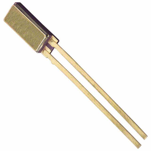
| 封装 | Tube |
| 封装/箱体 | TO-220-3 |
| 工厂包装数量 | 45 |
| 数字输出-位数 | None |
| 数字输出-总线接口 | - |
| 最大工作温度 | + 100 C |
| 最小工作温度 | 0 C |
| 标准包装 | 45 |
| 电源电压-最大 | 30 V |
| 电源电压-最小 | 4 V |
| 电源电流 | 80 uA |
| 系列 | LM35 |
| 设备功能 | Sensor |
| 输出类型 | Analog |
| 配置 | Local |


- 商务部:美国ITC正式对集成电路等产品启动337调查
- 曝三星4nm工艺存在良率问题 高通将骁龙8 Gen1或转产台积电
- 太阳诱电将投资9.5亿元在常州建新厂生产MLCC 预计2023年完工
- 英特尔发布欧洲新工厂建设计划 深化IDM 2.0 战略
- 台积电先进制程称霸业界 有大客户加持明年业绩稳了
- 达到5530亿美元!SIA预计今年全球半导体销售额将创下新高
- 英特尔拟将自动驾驶子公司Mobileye上市 估值或超500亿美元
- 三星加码芯片和SET,合并消费电子和移动部门,撤换高东真等 CEO
- 三星电子宣布重大人事变动 还合并消费电子和移动部门
- 海关总署:前11个月进口集成电路产品价值2.52万亿元 增长14.8%


PDF Datasheet 数据手册内容提取
Product Order Technical Tools & Support & Folder Now Documents Software Community LM35 SNIS159H–AUGUST1999–REVISEDDECEMBER2017 LM35 Precision Centigrade Temperature Sensors 1 Features 3 Description • CalibratedDirectlyinCelsius(Centigrade) The LM35 series are precision integrated-circuit 1 temperature devices with an output voltage linearly- • Linear+10-mV/°CScaleFactor proportional to the Centigrade temperature. The • 0.5°CEnsuredAccuracy(at25°C) LM35 device has an advantage over linear • RatedforFull−55°Cto150°CRange temperature sensors calibrated in Kelvin, as the user is not required to subtract a large constant voltage • SuitableforRemoteApplications from the output to obtain convenient Centigrade • Low-CostDuetoWafer-LevelTrimming scaling. The LM35 device does not require any • OperatesFrom4Vto30V external calibration or trimming to provide typical accuracies of ±¼°C at room temperature and ±¾°C • LessThan60-μACurrentDrain over a full −55°C to 150°C temperature range. Lower • LowSelf-Heating,0.08°CinStillAir cost is assured by trimming and calibration at the • Non-LinearityOnly±¼°CTypical wafer level. The low-output impedance, linear output, • Low-ImpedanceOutput,0.1 Ωfor1-mALoad and precise inherent calibration of the LM35 device makes interfacing to readout or control circuitry 2 Applications especially easy. The device is used with single power supplies, or with plus and minus supplies. As the • PowerSupplies LM35 device draws only 60 μA from the supply, it has • BatteryManagement verylowself-heatingoflessthan0.1°Cinstillair.The LM35 device is rated to operate over a −55°C to • HVAC 150°C temperature range, while the LM35C device is • Appliances rated for a −40°C to 110°C range (−10° with improved accuracy). The LM35-series devices are available packaged in hermetic TO transistor packages, while the LM35C, LM35CA, and LM35D devices are available in the plastic TO-92 transistor package. The LM35D device is available in an 8-lead surface-mount small-outline package and a plastic TO-220package. DeviceInformation(1) PARTNUMBER PACKAGE BODYSIZE(NOM) TO-CAN(3) 4.699mm×4.699mm TO-92(3) 4.30mm×4.30mm LM35 SOIC(8) 4.90mm×3.91mm TO-220(3) 14.986mm×10.16mm (1) For all available packages, see the orderable addendum at theendofthedatasheet. BasicCentigradeTemperatureSensor Full-RangeCentigradeTemperatureSensor (2°Cto150°C) +V S +V S (4 V to 20 V) LM35 VOUT OUTPUT LM35 R1 0 mV + 10.0 mV/(cid:176)C tV S ChooseR =–V /50µA 1 S V =1500mVat150°C OUT V =250mVat25°C OUT V =–550mVat–55°C OUT 1 An IMPORTANT NOTICE at the end of this data sheet addresses availability, warranty, changes, use in safety-critical applications, intellectualpropertymattersandotherimportantdisclaimers.PRODUCTIONDATA.
LM35 SNIS159H–AUGUST1999–REVISEDDECEMBER2017 www.ti.com Table of Contents 1 Features.................................................................. 1 7.3 FeatureDescription.................................................13 2 Applications........................................................... 1 7.4 DeviceFunctionalModes........................................13 3 Description............................................................. 1 8 ApplicationandImplementation........................ 14 4 RevisionHistory..................................................... 2 8.1 ApplicationInformation............................................14 8.2 TypicalApplication..................................................15 5 PinConfigurationandFunctions......................... 3 8.3 SystemExamples...................................................16 6 Specifications......................................................... 4 9 PowerSupplyRecommendations...................... 19 6.1 AbsoluteMaximumRatings......................................4 10 Layout................................................................... 19 6.2 ESDRatings..............................................................4 6.3 RecommendedOperatingConditions.......................4 10.1 LayoutGuidelines.................................................19 6.4 ThermalInformation..................................................4 10.2 LayoutExample....................................................20 6.5 ElectricalCharacteristics:LM35A,LM35CALimits...5 11 DeviceandDocumentationSupport................. 21 6.6 ElectricalCharacteristics:LM35A,LM35CA.............6 11.1 ReceivingNotificationofDocumentationUpdates21 6.7 ElectricalCharacteristics:LM35,LM35C,LM35D 11.2 CommunityResources..........................................21 Limits..........................................................................8 11.3 Trademarks...........................................................21 6.8 ElectricalCharacteristics:LM35,LM35C,LM35D ...9 11.4 ElectrostaticDischargeCaution............................21 6.9 TypicalCharacteristics............................................11 11.5 Glossary................................................................21 7 DetailedDescription............................................ 13 12 Mechanical,Packaging,andOrderable 7.1 Overview.................................................................13 Information........................................................... 21 7.2 FunctionalBlockDiagram.......................................13 4 Revision History ChangesfromRevisionG(August2016)toRevisionH Page • ChangedNDVPackage(TO-CAN)pinoutfrombottomviewbacktotopview;addedtextnotetopinout............................. 3 • AddedpinnumberstotheTO-CAN(TO46)pinout................................................................................................................ 3 ChangesfromRevisionF(January2016)toRevisionG Page • Equation1,changedFrom:10mV/°FTo:10mv/°C ............................................................................................................ 13 • PowerSupplyRecommendations,changedFrom:"4-Vto5.5-Vpowersupply"To:"4-Vto30-Vpowersupply:..............19 ChangesfromRevisionE(January2015)toRevisionF Page • ChangedNDVPackage(TO-CAN)pinoutfromTopViewtoBottomView........................................................................... 3 ChangesfromRevisionD(October2013)toRevisionE Page • AddedPinConfigurationandFunctionssection,ESDRatingstable,FeatureDescriptionsection,DeviceFunctional Modes,ApplicationandImplementationsection,PowerSupplyRecommendationssection,Layoutsection,Device andDocumentationSupportsection,andMechanical,Packaging,andOrderableInformationsection .............................. 1 ChangesfromRevisionC(July2013)toRevisionD Page • ChangedWtoΩ .................................................................................................................................................................... 1 • ChangedWtoΩinAbsMaxtablenote. ................................................................................................................................ 4 2 SubmitDocumentationFeedback Copyright©1999–2017,TexasInstrumentsIncorporated ProductFolderLinks:LM35
LM35 www.ti.com SNIS159H–AUGUST1999–REVISEDDECEMBER2017 5 Pin Configuration and Functions NDVPackage 3-PinTO-CAN LPPackage (TopView) 3-PinTO-92 (BottomView) (1) +VS (3) GND +VS VOUTGND (2) VOUT 1 2 3 Caseisconnectedtonegativepin(GND) ReferthesecondNDV0003Hpagefor reference NEBPackage 3-PinTO-220 (TopView) DPackage 8-PINSOIC (TopView) V 1 8 +V LM OUT S N.C. 2 7 N.C. 35DT 1 2 3 N.C. 3 6 N.C. GND 4 5 N.C. N.C.=Noconnection +V V S OUT GND Tabisconnectedtothenegativepin (GND). NOTE:TheLM35DTpinoutisdifferentthan thediscontinuedLM35DP PinFunctions PIN TYPE DESCRIPTION NAME TO46 TO92 TO220 SO8 V 2 2 3 1 O TemperatureSensorAnalogOutput OUT — — — 2 N.C. — NoConnection — — — 3 Devicegroundpin,connecttopowersupplynegative GND 3 3 2 4 GROUND terminal — — — 5 N.C. — — — 6 — NoConnection — — — 7 +V 1 1 1 8 POWER Positivepowersupplypin S Copyright©1999–2017,TexasInstrumentsIncorporated SubmitDocumentationFeedback 3 ProductFolderLinks:LM35
LM35 SNIS159H–AUGUST1999–REVISEDDECEMBER2017 www.ti.com 6 Specifications 6.1 Absolute Maximum Ratings overoperatingfree-airtemperaturerange(unlessotherwisenoted)(1)(2) MIN MAX UNIT Supplyvoltage –0.2 35 V Outputvoltage –1 6 V Outputcurrent 10 mA MaximumJunctionTemperature,Tmax 150 °C J TO-CAN,TO-92Package –60 150 StorageTemperature,T °C stg TO-220,SOICPackage –65 150 (1) IfMilitary/Aerospacespecifieddevicesarerequired,pleasecontacttheTexasInstrumentsSalesOffice/Distributorsforavailabilityand specifications. (2) AbsoluteMaximumRatingsindicatelimitsbeyondwhichdamagetothedevicemayoccur.DCandACelectricalspecificationsdonot applywhenoperatingthedevicebeyonditsratedoperatingconditions. 6.2 ESD Ratings VALUE UNIT V Electrostaticdischarge Human-bodymodel(HBM),perANSI/ESDA/JEDECJS-001(1) ±2500 V (ESD) (1) JEDECdocumentJEP155statesthat500-VHBMallowssafemanufacturingwithastandardESDcontrolprocess. 6.3 Recommended Operating Conditions overoperatingfree-airtemperaturerange(unlessotherwisenoted) MIN MAX UNIT LM35,LM35A –55 150 Specifiedoperatingtemperature:T to MIN LM35C,LM35CA –40 110 °C T MAX LM35D 0 100 SupplyVoltage(+V ) 4 30 V S 6.4 Thermal Information LM35 THERMALMETRIC(1)(2) NDV LP D NEB UNIT 3PINS 8PINS 3PINS R Junction-to-ambientthermalresistance 400 180 220 90 θJA °C/W R Junction-to-case(top)thermalresistance 24 — — — θJC(top) (1) Formoreinformationabouttraditionalandnewthermalmetrics,seetheICPackageThermalMetricsapplicationreport,SPRA953. (2) Foradditionalthermalresistanceinformation,seeTypicalApplication. 4 SubmitDocumentationFeedback Copyright©1999–2017,TexasInstrumentsIncorporated ProductFolderLinks:LM35
LM35 www.ti.com SNIS159H–AUGUST1999–REVISEDDECEMBER2017 6.5 Electrical Characteristics: LM35A, LM35CA Limits Unlessotherwisenoted,thesespecificationsapply:−55°C≤T ≤150°CfortheLM35andLM35A;−40°C≤T ≤110°Cforthe J J LM35CandLM35CA;and0°C≤T ≤100°CfortheLM35D.V =5VdcandI =50μA,inthecircuitofFull-Range J S LOAD CentigradeTemperatureSensor.Thesespecificationsalsoapplyfrom2°CtoT inthecircuitofFigure14. MAX LM35A LM35CA PARAMETER TESTCONDITIONS TYP TESTED DESIGN TYP TESTED DESIGN UNIT LIMIT(1) LIMIT(2) LIMIT(1) LIMIT(2) T =25°C ±0.2 ±0.5 ±0.2 ±0.5 A T =–10°C ±0.3 ±0.3 ±1 Accuracy(3) A °C T =T ±0.4 ±1 ±0.4 ±1 A MAX T =T ±0.4 ±1 ±0.4 ±1.5 A MIN Nonlinearity(4) TMIN≤TA≤TMAX, ±0.18 ±0.35 ±0.15 ±0.3 °C –40°C≤T ≤125°C J Sensorgain TMIN≤TA≤TMAX 10 9.9 10 9.9 mV/°C (averageslope) –40°C≤T ≤125°C 10 10.1 10 10.1 J T =25°C ±0.4 ±1 ±0.4 ±1 Loadregulation(5) A 0≤IL≤1mA TMIN≤TA≤TMAX, ±0.5 ±3 ±0.5 ±3 mV/mA –40°C≤T ≤125°C J T =25°C ±0.01 ±0.05 ±0.01 ±0.05 A Lineregulation(5) 4V≤V ≤30V, mV/V S ±0.02 ±0.1 ±0.02 ±0.1 –40°C≤T ≤125°C J V =5V,25°C 56 67 56 67 S V =5V,–40°C≤T ≤125°C 105 131 91 114 Quiescentcurrent(6) S J µA V =30V,25°C 56.2 68 56.2 68 S V =30V,–40°C≤T ≤125°C 105.5 133 91.5 116 S J 4V≤V ≤30V,25°C 0.2 1 0.2 1 S Changeofquiescent current(5) 4V≤VS≤30V, 0.5 2 0.5 2 µA –40°C≤T ≤125°C J Temperature coefficientof –40°C≤T ≤125°C 0.39 0.5 0.39 0.5 µA/°C J quiescentcurrent Minimumtemperature IncircuitofFigure14,I =0 1.5 2 1.5 2 °C forrateaccuracy L Longtermstability T =T ,for1000hours ±0.08 ±0.08 °C J MAX (1) TestedLimitsareensuredand100%testedinproduction. (2) DesignLimitsareensured(butnot100%productiontested)overtheindicatedtemperatureandsupplyvoltageranges.Theselimitsare notusedtocalculateoutgoingqualitylevels. (3) Accuracyisdefinedastheerrorbetweentheoutputvoltageand10mv/°Ctimesthecasetemperatureofthedevice,atspecified conditionsofvoltage,current,andtemperature(expressedin°C). (4) Non-linearityisdefinedasthedeviationoftheoutput-voltage-versus-temperaturecurvefromthebest-fitstraightline,overtherated temperaturerangeofthedevice. (5) Regulationismeasuredatconstantjunctiontemperature,usingpulsetestingwithalowdutycycle.Changesinoutputduetoheating effectscanbecomputedbymultiplyingtheinternaldissipationbythethermalresistance. (6) QuiescentcurrentisdefinedinthecircuitofFigure14. Copyright©1999–2017,TexasInstrumentsIncorporated SubmitDocumentationFeedback 5 ProductFolderLinks:LM35
LM35 SNIS159H–AUGUST1999–REVISEDDECEMBER2017 www.ti.com 6.6 Electrical Characteristics: LM35A, LM35CA Unlessotherwisenoted,thesespecificationsapply:−55°C≤T ≤150°CfortheLM35andLM35A;−40°C≤T ≤110°Cforthe J J LM35CandLM35CA;and0°C≤T ≤100°CfortheLM35D.V =5VdcandI =50μA,inthecircuitofFull-Range J S LOAD CentigradeTemperatureSensor.Thesespecificationsalsoapplyfrom2°CtoT inthecircuitofFigure14. MAX LM35A LM35CA PARAMETER TESTCONDITIONS UNIT MIN TYP MAX TYP TYP MAX ±0.2 ±0.2 T =25°C TestedLimit(2) ±0.5 ±0.5 A DesignLimit(3) ±0.3 ±0.3 T =–10°C TestedLimit(2) A DesignLimit(3) ±1 Accuracy(1) °C ±0.4 ±0.4 T =T TestedLimit(2) ±1 ±1 A MAX DesignLimit(3) ±0.4 ±0.4 T =T TestedLimit(2) ±1 A MIN DesignLimit(3) ±1.5 ±0.18 ±0.15 Nonlinearity(4) TMIN≤TA≤TMAX, TestedLimit(2) °C –40°C≤T ≤125°C J DesignLimit(3) ±0.35 ±0.3 10 10 T ≤T ≤T TestedLimit(2) 9.9 MIN A MAX Sensorgain DesignLimit(3) 9.9 mV/°C (averageslope) 10 10 –40°C≤T ≤125°C TestedLimit(2) 10.1 J DesignLimit(3) 10.1 ±0.4 ±0.4 T =25°C TestedLimit(2) ±1 ±1 A Loadregulation(5) DesignLimit(3) mV/mA 0≤IL≤1mA ±0.5 ±0.5 TMIN≤TA≤TMAX, TestedLimit(2) –40°C≤T ≤125°C J DesignLimit(3) ±3 ±3 ±0.01 ±0.01 T =25°C TestedLimit(2) ±0.05 ±0.05 A DesignLimit(3) Lineregulation(5) mV/V ±0.02 ±0.02 4V≤VS≤30V, TestedLimit(2) –40°C≤T ≤125°C J DesignLimit(3) ±0.1 ±0.1 (1) Accuracyisdefinedastheerrorbetweentheoutputvoltageand10mv/°Ctimesthecasetemperatureofthedevice,atspecified conditionsofvoltage,current,andtemperature(expressedin°C). (2) TestedLimitsareensuredand100%testedinproduction. (3) DesignLimitsareensured(butnot100%productiontested)overtheindicatedtemperatureandsupplyvoltageranges.Theselimitsare notusedtocalculateoutgoingqualitylevels. (4) Non-linearityisdefinedasthedeviationoftheoutput-voltage-versus-temperaturecurvefromthebest-fitstraightline,overtherated temperaturerangeofthedevice. (5) Regulationismeasuredatconstantjunctiontemperature,usingpulsetestingwithalowdutycycle.Changesinoutputduetoheating effectscanbecomputedbymultiplyingtheinternaldissipationbythethermalresistance. 6 SubmitDocumentationFeedback Copyright©1999–2017,TexasInstrumentsIncorporated ProductFolderLinks:LM35
LM35 www.ti.com SNIS159H–AUGUST1999–REVISEDDECEMBER2017 Electrical Characteristics: LM35A, LM35CA (continued) Unlessotherwisenoted,thesespecificationsapply:−55°C≤T ≤150°CfortheLM35andLM35A;−40°C≤T ≤110°Cforthe J J LM35CandLM35CA;and0°C≤T ≤100°CfortheLM35D.V =5VdcandI =50μA,inthecircuitofFull-Range J S LOAD CentigradeTemperatureSensor.Thesespecificationsalsoapplyfrom2°CtoT inthecircuitofFigure14. MAX LM35A LM35CA PARAMETER TESTCONDITIONS UNIT MIN TYP MAX TYP TYP MAX 56 56 V =5V,25°C TestedLimit(2) 67 67 S DesignLimit(3) 105 91 VS=5V, TestedLimit(2) –40°C≤T ≤125°C J Quiescent DesignLimit(3) 131 114 current(6) 56.2 56.2 µA V =30V,25°C TestedLimit(2) 68 68 S DesignLimit(3) 105.5 91.5 VS=30V, TestedLimit(2) –40°C≤T ≤125°C J DesignLimit(3) 133 116 0.2 0.2 4V≤V ≤30V,25°C TestedLimit(2) 1 1 S Changeof DesignLimit(3) quiescent µA current(5) 0.5 0.5 4V≤VS≤30V, TestedLimit(2) –40°C≤T ≤125°C J DesignLimit(3) 2 2 0.39 0.39 Temperature coefficientof –40°C≤T ≤125°C TestedLimit(2) µA/°C J quiescentcurrent DesignLimit(3) 0.5 0.5 1.5 1.5 Minimum temperaturefor IncircuitofFigure14,IL= TestedLimit(2) °C 0 rateaccuracy DesignLimit(3) 2 2 Longterm ±0.08 ±0.08 T =T ,for1000hours °C stability J MAX (6) QuiescentcurrentisdefinedinthecircuitofFigure14. Copyright©1999–2017,TexasInstrumentsIncorporated SubmitDocumentationFeedback 7 ProductFolderLinks:LM35
LM35 SNIS159H–AUGUST1999–REVISEDDECEMBER2017 www.ti.com 6.7 Electrical Characteristics: LM35, LM35C, LM35D Limits Unlessotherwisenoted,thesespecificationsapply:−55°C≤T ≤150°CfortheLM35andLM35A;−40°C≤T ≤110°Cforthe J J LM35CandLM35CA;and0°C≤T ≤100°CfortheLM35D.V =5VdcandI =50μA,inthecircuitofFull-Range J S LOAD CentigradeTemperatureSensor.Thesespecificationsalsoapplyfrom2°CtoT inthecircuitofFigure14. MAX LM35 LM35C,LM35D PARAMETER TESTCONDITIONS TYP TESTED DESIGN TYP TESTED DESIGN UNIT LIMIT(1) LIMIT(2) LIMIT(1) LIMIT(2) T =25°C ±0.4 ±1 ±0.4 ±1 A Accuracy,LM35, TA=–10°C ±0.5 ±0.5 ±1.5 LM35C(3) T =T ±0.8 ±1.5 ±0.8 ±1.5 °C A MAX T =T ±0.8 ±1.5 ±0.8 ±2 A MIN T =25°C ±0.6 ±1.5 A Accuracy,LM35D(3) T =T ±0.9 ±2 °C A MAX T =T ±0.9 ±2 A MIN Nonlinearity(4) TMIN≤TA≤TMAX, ±0.3 ±0.5 ±0.2 ±0.5 °C –40°C≤T ≤125°C J T ≤T ≤T , Sensorgain –4M0IN°C≤ATJ≤M1A2X5°C 10 9.8 10 9.8 mV/°C (averageslope) 10 10.2 10 10.2 T =25°C ±0.4 ±2 ±0.4 ±2 Loadregulation(5) A 0≤IL≤1mA TMIN≤TA≤TMAX, ±0.5 ±5 ±0.5 ±5 mV/mA –40°C≤T ≤125°C J T =25°C ±0.01 ±0.1 ±0.01 ±0.1 A Lineregulation(5) 4V≤V ≤30V, mV/V S ±0.02 ±0.2 ±0.02 ±0.2 –40°C≤T ≤125°C J V =5V,25°C 56 80 56 80 S V =5V,–40°C≤T ≤125°C 105 158 91 138 Quiescentcurrent(6) S J µA V =30V,25°C 56.2 82 56.2 82 S V =30V,–40°C≤T ≤125°C 105.5 161 91.5 141 S J 4V≤V ≤30V,25°C 0.2 2 0.2 2 S Changeofquiescent current(5) 4V≤VS≤30V, 0.5 3 0.5 3 µA –40°C≤T ≤125°C J Temperature coefficientof –40°C≤T ≤125°C 0.39 0.7 0.39 0.7 µA/°C J quiescentcurrent Minimumtemperature IncircuitofFigure14,I =0 1.5 2 1.5 2 °C forrateaccuracy L Longtermstability T =T ,for1000hours ±0.08 ±0.08 °C J MAX (1) TestedLimitsareensuredand100%testedinproduction. (2) DesignLimitsareensured(butnot100%productiontested)overtheindicatedtemperatureandsupplyvoltageranges.Theselimitsare notusedtocalculateoutgoingqualitylevels. (3) Accuracyisdefinedastheerrorbetweentheoutputvoltageand10mv/°Ctimesthecasetemperatureofthedevice,atspecified conditionsofvoltage,current,andtemperature(expressedin°C). (4) Non-linearityisdefinedasthedeviationoftheoutput-voltage-versus-temperaturecurvefromthebest-fitstraightline,overtherated temperaturerangeofthedevice. (5) Regulationismeasuredatconstantjunctiontemperature,usingpulsetestingwithalowdutycycle.Changesinoutputduetoheating effectscanbecomputedbymultiplyingtheinternaldissipationbythethermalresistance. (6) QuiescentcurrentisdefinedinthecircuitofFigure14. 8 SubmitDocumentationFeedback Copyright©1999–2017,TexasInstrumentsIncorporated ProductFolderLinks:LM35
LM35 www.ti.com SNIS159H–AUGUST1999–REVISEDDECEMBER2017 6.8 Electrical Characteristics: LM35, LM35C, LM35D Unlessotherwisenoted,thesespecificationsapply:−55°C≤T ≤150°CfortheLM35andLM35A;−40°C≤T ≤110°Cforthe J J LM35CandLM35CA;and0°C≤T ≤100°CfortheLM35D.V =5VdcandI =50μA,inthecircuitofFull-Range J S LOAD CentigradeTemperatureSensor.Thesespecificationsalsoapplyfrom2°CtoT inthecircuitofFigure14. MAX LM35 LM35C,LM35D PARAMETER TESTCONDITIONS UNIT MIN TYP MAX MIN TYP MAX ±0.4 ±0.4 T =25°C TestedLimit(2) ±1 ±1 A DesignLimit(3) ±0.5 ±0.5 T =–10°C TestedLimit(2) A Accuracy,LM35, DesignLimit(3) ±1.5 LM35C(1) ±0.8 ±0.8 °C T =T TestedLimit(2) ±1.5 A MAX DesignLimit(3) ±1.5 ±0.8 ±0.8 T =T TestedLimit(2) A MIN DesignLimit(3) ±1.5 ±2 ±0.6 T =25°C TestedLimit(2) ±1.5 A DesignLimit(3) ±0.9 ALMcc3u5rDac(1y), TA=TMAX TestedLimit(2) °C DesignLimit(3) ±2 ±0.9 T =T TestedLimit(2) A MIN DesignLimit(3) ±2 ±0.3 ±0.2 Nonlinearity(4) TMIN≤TA≤TMAX, TestedLimit(2) °C –40°C≤T ≤125°C J DesignLimit(3) ±0.5 ±0.5 10 10 TMIN≤TA≤TMAX, TestedLimit(2) 9.8 –40°C≤T ≤125°C J Sensorgain DesignLimit(3) 9.8 mV/°C (averageslope) 10 10 TestedLimit(2) 10.2 DesignLimit(3) 10.2 ±0.4 ±0.4 T =25°C TestedLimit(2) ±2 ±2 A Loadregulation(5) DesignLimit(3) mV/mA 0≤IL≤1mA ±0.5 ±0.5 TMIN≤TA≤TMAX, TestedLimit(2) –40°C≤T ≤125°C J DesignLimit(3) ±5 ±5 (1) Accuracyisdefinedastheerrorbetweentheoutputvoltageand10mv/°Ctimesthecasetemperatureofthedevice,atspecified conditionsofvoltage,current,andtemperature(expressedin°C). (2) TestedLimitsareensuredand100%testedinproduction. (3) DesignLimitsareensured(butnot100%productiontested)overtheindicatedtemperatureandsupplyvoltageranges.Theselimitsare notusedtocalculateoutgoingqualitylevels. (4) Non-linearityisdefinedasthedeviationoftheoutput-voltage-versus-temperaturecurvefromthebest-fitstraightline,overtherated temperaturerangeofthedevice. (5) Regulationismeasuredatconstantjunctiontemperature,usingpulsetestingwithalowdutycycle.Changesinoutputduetoheating effectscanbecomputedbymultiplyingtheinternaldissipationbythethermalresistance. Copyright©1999–2017,TexasInstrumentsIncorporated SubmitDocumentationFeedback 9 ProductFolderLinks:LM35
LM35 SNIS159H–AUGUST1999–REVISEDDECEMBER2017 www.ti.com Electrical Characteristics: LM35, LM35C, LM35D (continued) Unlessotherwisenoted,thesespecificationsapply:−55°C≤T ≤150°CfortheLM35andLM35A;−40°C≤T ≤110°Cforthe J J LM35CandLM35CA;and0°C≤T ≤100°CfortheLM35D.V =5VdcandI =50μA,inthecircuitofFull-Range J S LOAD CentigradeTemperatureSensor.Thesespecificationsalsoapplyfrom2°CtoT inthecircuitofFigure14. MAX LM35 LM35C,LM35D PARAMETER TESTCONDITIONS UNIT MIN TYP MAX MIN TYP MAX ±0.01 ±0.01 T =25°C TestedLimit(2) ±0.1 A DesignLimit(3) ±0.1 Lineregulation(5) mV/V ±0.02 ±0.02 4V≤VS≤30V, TestedLimit(2) –40°C≤T ≤125°C J DesignLimit(3) ±0.2 ±0.2 56 56 V =5V,25°C TestedLimit(2) 80 80 S DesignLimit(3) 105 91 VS=5V,–40°C≤TJ≤ TestedLimit(2) 125°C Quiescent DesignLimit(3) 158 138 current(6) 56.2 56.2 µA V =30V,25°C TestedLimit(2) 82 82 S DesignLimit(3) 105.5 91.5 VS=30V, TestedLimit(2) –40°C≤T ≤125°C J DesignLimit(3) 161 141 0.2 0.2 4V≤V ≤30V,25°C TestedLimit(2) 2 S Changeof DesignLimit(3) 2 quiescent µA current(5) 0.5 0.5 4V≤VS≤30V, TestedLimit(2) –40°C≤T ≤125°C J DesignLimit(3) 3 3 0.39 0.39 Temperature coefficientof –40°C≤T ≤125°C TestedLimit(2) µA/°C J quiescentcurrent DesignLimit(3) 0.7 0.7 1.5 1.5 Minimum temperaturefor IncircuitofFigure14,I =0 TestedLimit(2) °C L rateaccuracy DesignLimit(3) 2 2 Longterm ±0.08 ±0.08 T =T ,for1000hours °C stability J MAX (6) QuiescentcurrentisdefinedinthecircuitofFigure14. 10 SubmitDocumentationFeedback Copyright©1999–2017,TexasInstrumentsIncorporated ProductFolderLinks:LM35
LM35 www.ti.com SNIS159H–AUGUST1999–REVISEDDECEMBER2017 6.9 Typical Characteristics 400 45 W) 40 (cid:131)NCE (C/300 T (SEC) 3305 TA AN25 ESIS200 T0-46 NST20 R O AL E C15 T0-46 M M ER100 TI10 H T0-92 T 5 T0-92 0 0 0 400 800 1200 1600 2000 0 400 800 1200 1600 2000 AIR VELOCITY (FPM) C001 AIR VELOCITY (FPM) C002 Figure1.ThermalResistanceJunctionToAir Figure2.ThermalTimeConstant 120 120 %) 100 %) 100 E ( E ( LU 80 LU 80 T0-46 A A V V AL 60 AL 60 N N FI FI T0-92 F 40 F 40 O O T T EN 20 EN 20 C C R R PE 0 PE 0 –20 –20 0 2 4 6 8 0 2 4 6 8 TIME (MINUTES) C003 TIME (SEC) C004 Figure3.ThermalResponseInStillAir Figure4.ThermalResponseInStirredOilBath 4.4 160 4.2 TYPICAL 140 4.0 IOUT = 2.0 mA A) E (V) 3.8 (cid:29)NT (120 AG3.6 RE100 T R OL3.4 CU 80 SUPPLY V233...802 TYPICAL TIOYUTP I=C 1A.L0 mA UIESCENT 4600 I = 0 (cid:29)A or 50 (cid:29)A Q 2.6 OUT 20 2.4 0 –75 –25 25 75 125 175 –75 –25 25 75 125 175 TEMPERATURE ((cid:131)C) C005 TEMPERATURE ((cid:131)C) C006 Figure5.MinimumSupplyVoltagevsTemperature Figure6.QuiescentCurrentvsTemperature(inCircuitof Figure14) Copyright©1999–2017,TexasInstrumentsIncorporated SubmitDocumentationFeedback 11 ProductFolderLinks:LM35
LM35 SNIS159H–AUGUST1999–REVISEDDECEMBER2017 www.ti.com Typical Characteristics (continued) 200 2.0 180 1.5 LM35 A) C) (cid:29)NT (160 (cid:131)OR ( 1.0 RRE140 ERR 0.5 TYPICAL LM35A CU120 RE 0.0 T U CEN100 RAT –0.5 LM35A S E QUIE 6800 TEMP ––11..50 LM35 40 –2.0 –75 –25 25 75 125 175 –75 –25 25 75 125 175 TEMPERATURE ((cid:131)C) C007 TEMPERATURE ((cid:131)C) C008 Figure7.QuiescentCurrentvsTemperature(inCircuitof Figure8.AccuracyvsTemperature(Ensured) Full-RangeCentigradeTemperatureSensor) 2.5 1600 2.0 LM35D 1400 C) 1.5 LM35C (cid:131)RROR ( 01..50 LM35CA Hz) 11020000 URE E 0.0 TYPICAL (cid:151)e (nV/ 800 RAT –0.5 LM35CA Nois 600 E –1.0 MP 400 E –1.5 LM35C T –2.0 200 –2.5 0 –75 –25 25 75 125 175 10 100 1k 10k 100k TEMPERATURE ((cid:131)C) FREQUENCY (Hz) C009 C010 Figure9.AccuracyvsTemperature(Ensured) Figure10.NoiseVoltage 6 V) 4 (N VI 2 0 0.6 0.4 V) (UT 0.2 O V 0 -0.2 -20 -10 0 10 20 30 40 50 60 TIME ((cid:29)SEC) C011 Figure11.Start-UpResponse 12 SubmitDocumentationFeedback Copyright©1999–2017,TexasInstrumentsIncorporated ProductFolderLinks:LM35
LM35 www.ti.com SNIS159H–AUGUST1999–REVISEDDECEMBER2017 7 Detailed Description 7.1 Overview The LM35-series devices are precision integrated-circuit temperature sensors, with an output voltage linearly proportional to the Centigrade temperature. The LM35 device has an advantage over linear temperature sensors calibrated in Kelvin, as the user is not required to subtract a large constant voltage from the output to obtain convenient Centigrade scaling. The LM35 device does not require any external calibration or trimming to provide typical accuracies of ± ¼ °C at room temperature and ± ¾ °C over a full −55°C to 150°C temperature range. Lower cost is assured by trimming and calibration at the wafer level. The low output impedance, linear output, and precise inherent calibration of the LM35 device makes interfacing to readout or control circuitry especially easy. The device is used with single power supplies, or with plus and minus supplies. As the LM35 device draws only 60 μA from the supply, it has very low self-heating of less than 0.1°C in still air. The LM35 device is rated to operate over a −55°C to 150°C temperature range, while the LM35C device is rated for a −40°C to 110°C range (−10° withimprovedaccuracy).Thetemperature-sensingelementiscomprisedofadelta-VBEarchitecture. The temperature-sensing element is then buffered by an amplifier and provided to the VOUT pin. The amplifier has a simple class A output stage with typical 0.5-Ω output impedance as shown in the Functional Block Diagram.ThereforetheLM35canonlysourcecurrentandit'ssinkingcapabilityislimitedto1 μA. 7.2 Functional Block Diagram A1 1.38 V PTAT +V S nR1 Q1 Q2 + A2 10E E V = 10 mV/(cid:176)C OUT V 0 .125 R2 nR1 8.8 mV/(cid:176)C R2 i 7.3 Feature Description 7.3.1 LM35TransferFunction TheaccuracyspecificationsoftheLM35aregivenwithrespecttoasimplelineartransferfunction: V =10mv/°C×T OUT where • V istheLM35outputvoltage OUT • Tisthetemperaturein°C (1) 7.4 Device Functional Modes TheonlyfunctionalmodeoftheLM35isthatithasananalogoutputdirectlyproportionaltotemperature. Copyright©1999–2017,TexasInstrumentsIncorporated SubmitDocumentationFeedback 13 ProductFolderLinks:LM35
LM35 SNIS159H–AUGUST1999–REVISEDDECEMBER2017 www.ti.com 8 Application and Implementation NOTE Information in the following applications sections is not part of the TI component specification, and TI does not warrant its accuracy or completeness. TI’s customers are responsible for determining suitability of components for their purposes. Customers should validateandtesttheirdesignimplementationtoconfirmsystemfunctionality. 8.1 Application Information The features of the LM35 make it suitable for many general temperature sensing applications. Multiple package optionsexpandonit'sflexibility. 8.1.1 CapacitiveDriveCapability Like most micropower circuits, the LM35 device has a limited ability to drive heavy capacitive loads. Alone, the LM35 device is able to drive 50 pF without special precautions. If heavier loads are anticipated, isolating or decoupling the load with a resistor is easy (see Figure 12). The tolerance of capacitance can be improved with a seriesR-Cdamperfromoutputtoground(seeFigure13). When the LM35 device is applied with a 200-Ω load resistor as shown in Figure 16, Figure 17, or Figure 19, the device is relatively immune to wiring capacitance because the capacitance forms a bypass from ground to input and not on the output. However, as with any linear circuit connected to wires in a hostile environment, performance is affected adversely by intense electromagnetic sources (such as relays, radio transmitters, motors with arcing brushes, and SCR transients), because the wiring acts as a receiving antenna and the internal junctionsactasrectifiers.Forbestresultsinsuchcases,abypasscapacitorfromV togroundandaseriesR-C IN damper, such as 75 Ω in series with 0.2 or 1 μF from output to ground, are often useful. Examples are shown in Figure13,Figure24,andFigure25. HEAVY CAPACITIVE LOAD, WIRING, ETC. + 2 k LM35 TO A HIGH-IMPEDANCE LOAD OUT v Figure12. LM35withDecouplingfromCapacitiveLoad HEAVY CAPACITIVE LOAD, WIRING, ETC. + OUT LM35 TO A HIGH-IMPEDANCE LOAD 0.01 PF BYPASS OPTONAL v 75 1 PF Figure13. LM35withR-CDamper 14 SubmitDocumentationFeedback Copyright©1999–2017,TexasInstrumentsIncorporated ProductFolderLinks:LM35
LM35 www.ti.com SNIS159H–AUGUST1999–REVISEDDECEMBER2017 8.2 Typical Application 8.2.1 BasicCentigradeTemperatureSensor +V S (4 V to 20 V) OUTPUT LM35 0 mV + 10.0 mV/(cid:176)C Figure14. BasicCentigradeTemperatureSensor(2 °Cto150 °C) 8.2.1.1 DesignRequirements Table1.DesignParameters PARAMETER VALUE Accuracyat25°C ±0.5°C Accuracyfrom–55°Cto150°C ±1°C TemperatureSlope 10mV/°C 8.2.1.2 DetailedDesignProcedure Because the LM35 device is a simple temperature sensor that provides an analog output, design requirements relatedtolayoutaremoreimportantthanelectricalrequirements.Foradetaileddescription,refertotheLayout. 8.2.1.3 ApplicationCurve 2.0 1.5 LM35 C) (cid:131)R ( 1.0 O ERR 0.5 TYPICAL LM35A RE 0.0 U RAT –0.5 LM35A E MP –1.0 E T –1.5 LM35 –2.0 –75 –25 25 75 125 175 TEMPERATURE ((cid:131)C) C008 Figure15. AccuracyvsTemperature(Ensured) Copyright©1999–2017,TexasInstrumentsIncorporated SubmitDocumentationFeedback 15 ProductFolderLinks:LM35
LM35 SNIS159H–AUGUST1999–REVISEDDECEMBER2017 www.ti.com 8.3 System Examples 5 V 5 V + + OUT HEAT LM35 VOUT = 10 mV/(cid:176)C (TAMBIENT = 1 (cid:176)C) FINS TWISTED PAIR 6.8 k 200 FROM + 2 (cid:176)C TO + 40 (cid:176)C v 200 5% 1% 1% v VOUT = 10 mV/(cid:176)C (TAMBIENT = 1 (cid:176)C) FROM + 2 (cid:176)C TO + 40 (cid:176)C + 6.8 k HEAT LM35 OUT 5% 200 FINS TWISTED PAIR OR 10K RHEOSTAT 1% v 200 FOR GAIN ADJUST 1% Figure16.Two-WireRemoteTemperatureSensor Figure17.Two-WireRemoteTemperatureSensor (GroundedSensor) (OutputReferredtoGround) +V S + 5 V OUT LM35 0.01 PF BYPASS TWISTED PAIR OPTIONAL LM35 + 2 k 200 1% 1% VOUT VFROUOTM = 1t0 5 m (cid:176)CV /T(cid:176)OC +(T 4A0M B(cid:176)ICENT = 10 (cid:176)C) 2 k 200 v 1% 1% 1N914 18 k 10% Figure18.TemperatureSensor,SingleSupply Figure19.Two-WireRemoteTemperatureSensor (−55° to+150°C) (OutputReferredtoGround) 16 SubmitDocumentationFeedback Copyright©1999–2017,TexasInstrumentsIncorporated ProductFolderLinks:LM35
LM35 www.ti.com SNIS159H–AUGUST1999–REVISEDDECEMBER2017 System Examples (continued) + 5 V TO + 30 V +VS (6 V to 20 V) 4.7 k 2N2907 LM35 + IN 45.5 kO OUT OUT LM35 LM317 1% v 402 ADJ 1% 62.5 10 kO 0.5% OFFSET 1% ADJUST 50 V = +1 mV/(cid:176)F OUT 26.4 kO 1% LM385-1.2 18 kO 1 MO 1% Figure20.4-To-20mACurrentSource Figure21.FahrenheitThermometer (0°Cto100°C) 5 V 9 V 1 k LM35 LM35 100 (cid:29)A, 60 mV FULL- SCALE 25.5 k LM385- 2.5 Figure22.CentigradeThermometer Figure23.FahrenheitThermometer,Expanded (AnalogMeter) ScaleThermometer (50°Fto80°F,forExampleShown) Copyright©1999–2017,TexasInstrumentsIncorporated SubmitDocumentationFeedback 17 ProductFolderLinks:LM35
LM35 SNIS159H–AUGUST1999–REVISEDDECEMBER2017 www.ti.com System Examples (continued) 5 V 5 V + 3.9 k + 16 k PARALLEL LM35 OUT REINF ADC08031 SDEARTIAA LOUTPUT LM35 OUT IN 8 DOAUTTAPUT 1.28 V GND GND ADC0804 75 100k + 75 INTR FB LM385 CLOCK 1 k + 0.V6R4EF V 1 PF + 10 k ENABLE 1 PF + 2 k CRSD GND WR GND Figure24.TemperaturetoDigitalConverter Figure25.TemperaturetoDigitalConverter (SerialOutput) (ParallelTRI-STATEOutputsforStandardDataBus (128°CFullScale) toμPInterface) (128°CFullScale) (cid:176)F 6 V 20 k 6.8 k 1 k 67 68 69 70 71 72 73 74 75 76 77 78 79 80 81 82 83 84 85 86 7 V + 20 PF fOUT 20 LEDs 4N28 18 10 18 10 + 100 k 8 LM3914 LM3914 LM35 7 5 1 2 3 4 5 6 7 8 9 1 2 3 4 5 6 7 8 9 LM131 7 V 1.2 k* 7 V NC GND 6 3 HFIENAST LM3+5 OUTVA200* VC 499* 499* VB 0.01 PF 100 k 1 PF 1 2FSA1UCD2LAJ LLkE4 0.01 PF 1.5 k* 1 k* 47 5 k LOW TEMPCO +1 PF 1.5 k* R1 Ck R1 Bk RA 1 k *=1%or2%filmresistor TrimR forV =3.075V B B TrimR forV =1.955V C C TrimR forV =0.075V+100mV/°C×T A A ambient Example,V =2.275Vat22°C A Figure26.Bar-GraphTemperatureDisplay Figure27.LM35WithVoltage-To-Frequency (DotMode) ConverterandIsolatedOutput (2°Cto150°C;20to1500Hz) 18 SubmitDocumentationFeedback Copyright©1999–2017,TexasInstrumentsIncorporated ProductFolderLinks:LM35
LM35 www.ti.com SNIS159H–AUGUST1999–REVISEDDECEMBER2017 9 Power Supply Recommendations The LM35 device has a very wide 4-V to 30-V power supply voltage range, which makes it ideal for many applications. In noisy environments, TI recommends adding a 0.1 μF from V+ to GND to bypass the power supplyvoltage.Largercapacitancesmayberequiredandaredependentonthepower-supplynoise. 10 Layout 10.1 Layout Guidelines The LM35 is easily applied in the same way as other integrated-circuit temperature sensors. Glue or cement the devicetoasurfaceandthetemperatureshouldbewithinabout0.01°Cofthesurfacetemperature. The 0.01°C proximity presumes that the ambient air temperature is almost the same as the surface temperature. If the air temperature were much higher or lower than the surface temperature, the actual temperature of the LM35 die would be at an intermediate temperature between the surface temperature and the air temperature; this is especially true for the TO-92 plastic package. The copper leads in the TO-92 package are the principal thermal path to carry heat into the device, so its temperature might be closer to the air temperature than to the surfacetemperature. Ensure that the wiring leaving the LM35 device is held at the same temperature as the surface of interest to minimize the temperature problem. The easiest fix is to cover up these wires with a bead of epoxy. The epoxy bead will ensure that the leads and wires are all at the same temperature as the surface, and that the temperatureoftheLM35dieisnotaffectedbytheairtemperature. The TO-46 metal package can also be soldered to a metal surface or pipe without damage. Of course, in that case the V− terminal of the circuit will be grounded to that metal. Alternatively, mount the LM35 inside a sealed- endmetaltube,andthendipintoabathorscrewintoathreadedholeinatank.AswithanyIC,theLM35device and accompanying wiring and circuits must be kept insulated and dry, to avoid leakage and corrosion. This is especially true if the circuit may operate at cold temperatures where condensation can occur. Printed-circuit coatings and varnishes such as a conformal coating and epoxy paints or dips are often used to insure that moisturecannotcorrodetheLM35deviceoritsconnections. These devices are sometimes soldered to a small light-weight heat fin to decrease the thermal time constant and speed up the response in slowly-moving air. On the other hand, a small thermal mass may be added to the sensor,togivethesteadiestreadingdespitesmalldeviationsintheairtemperature. Table2.TemperatureRiseofLM35DueToSelf-heating(ThermalResistance,R ) θJA TO,noheat TO(1),small TO-92,noheat TO-92(2),small SOIC-8,no SOIC-8(2), TO-220,no smallheat sink heatfin sink heatfin heatsink heatsink fin Stillair 400°C/W 100°C/W 180°C/W 140°C/W 220°C/W 110°C/W 90°C/W Movingair 100°C/W 40°C/W 90°C/W 70°C/W 105°C/W 90°C/W 26°C/W Stilloil 100°C/W 40°C/W 90°C/W 70°C/W — — — Stirredoil 50°C/W 30°C/W 45°C/W 40°C/W — — — (Clampedto metal,Infinite (24°C/W) — — (55°C/W) — heatsink) (1) Wakefieldtype201,or1-indiscof0.02-insheetbrass,solderedtocase,orsimilar. (2) TO-92andSOIC-8packagesgluedandleadssolderedto1-insquareof1/16-inprintedcircuitboardwith2-ozfoilorsimilar. Copyright©1999–2017,TexasInstrumentsIncorporated SubmitDocumentationFeedback 19 ProductFolderLinks:LM35
LM35 SNIS159H–AUGUST1999–REVISEDDECEMBER2017 www.ti.com 10.2 Layout Example VIA to ground plane VIA to power plane V +V OUT S N.C. N.C. 0.01 µF N.C. N.C. GND N.C. Figure28. LayoutExample 20 SubmitDocumentationFeedback Copyright©1999–2017,TexasInstrumentsIncorporated ProductFolderLinks:LM35
LM35 www.ti.com SNIS159H–AUGUST1999–REVISEDDECEMBER2017 11 Device and Documentation Support 11.1 Receiving Notification of Documentation Updates To receive notification of documentation updates, navigate to the device product folder on ti.com. In the upper right corner, click on Alert me to register and receive a weekly digest of any product information that has changed.Forchangedetails,reviewtherevisionhistoryincludedinanyreviseddocument 11.2 Community Resources The following links connect to TI community resources. Linked contents are provided "AS IS" by the respective contributors. They do not constitute TI specifications and do not necessarily reflect TI's views; see TI's Terms of Use. TIE2E™OnlineCommunity TI'sEngineer-to-Engineer(E2E)Community.Createdtofostercollaboration amongengineers.Ate2e.ti.com,youcanaskquestions,shareknowledge,exploreideasandhelp solveproblemswithfellowengineers. DesignSupport TI'sDesignSupport QuicklyfindhelpfulE2Eforumsalongwithdesignsupporttoolsand contactinformationfortechnicalsupport. 11.3 Trademarks E2EisatrademarkofTexasInstruments. Allothertrademarksarethepropertyoftheirrespectiveowners. 11.4 Electrostatic Discharge Caution Thesedeviceshavelimitedbuilt-inESDprotection.Theleadsshouldbeshortedtogetherorthedeviceplacedinconductivefoam duringstorageorhandlingtopreventelectrostaticdamagetotheMOSgates. 11.5 Glossary SLYZ022—TIGlossary. Thisglossarylistsandexplainsterms,acronyms,anddefinitions. 12 Mechanical, Packaging, and Orderable Information The following pages include mechanical, packaging, and orderable information. This information is the most current data available for the designated devices. This data is subject to change without notice and revision of thisdocument.Forbrowser-basedversionsofthisdatasheet,refertotheleft-handnavigation. Copyright©1999–2017,TexasInstrumentsIncorporated SubmitDocumentationFeedback 21 ProductFolderLinks:LM35
PACKAGE OPTION ADDENDUM www.ti.com 6-Feb-2020 PACKAGING INFORMATION Orderable Device Status Package Type Package Pins Package Eco Plan Lead/Ball Finish MSL Peak Temp Op Temp (°C) Device Marking Samples (1) Drawing Qty (2) (6) (3) (4/5) LM35AH ACTIVE TO NDV 3 500 TBD Call TI Call TI -55 to 150 ( LM35AH, LM35AH) LM35AH/NOPB ACTIVE TO NDV 3 500 Green (RoHS Call TI Level-1-NA-UNLIM -55 to 150 ( LM35AH, LM35AH) & no Sb/Br) LM35CAH ACTIVE TO NDV 3 500 TBD Call TI Call TI -40 to 110 ( LM35CAH, LM35CAH ) LM35CAH/NOPB ACTIVE TO NDV 3 500 Green (RoHS Call TI Level-1-NA-UNLIM -40 to 110 ( LM35CAH, LM35CAH & no Sb/Br) ) LM35CAZ/LFT4 ACTIVE TO-92 LP 3 2000 Green (RoHS SN N / A for Pkg Type LM35 & no Sb/Br) CAZ LM35CAZ/NOPB ACTIVE TO-92 LP 3 1800 Green (RoHS SN N / A for Pkg Type -40 to 110 LM35 & no Sb/Br) CAZ LM35CH ACTIVE TO NDV 3 500 TBD Call TI Call TI -40 to 110 ( LM35CH, LM35CH) LM35CH/NOPB ACTIVE TO NDV 3 500 Green (RoHS Call TI Level-1-NA-UNLIM -40 to 110 ( LM35CH, LM35CH) & no Sb/Br) LM35CZ/LFT1 ACTIVE TO-92 LP 3 2000 Green (RoHS SN N / A for Pkg Type LM35 & no Sb/Br) CZ LM35CZ/NOPB ACTIVE TO-92 LP 3 1800 Green (RoHS SN N / A for Pkg Type -40 to 110 LM35 & no Sb/Br) CZ LM35DH ACTIVE TO NDV 3 1000 TBD Call TI Call TI 0 to 70 ( LM35DH, LM35DH) LM35DH/NOPB ACTIVE TO NDV 3 1000 Green (RoHS Call TI Level-1-NA-UNLIM 0 to 70 ( LM35DH, LM35DH) & no Sb/Br) LM35DM NRND SOIC D 8 95 TBD Call TI Call TI 0 to 100 LM35D M LM35DM/NOPB ACTIVE SOIC D 8 95 Green (RoHS SN Level-1-260C-UNLIM 0 to 100 LM35D & no Sb/Br) M LM35DMX NRND SOIC D 8 2500 TBD Call TI Call TI 0 to 100 LM35D M LM35DMX/NOPB ACTIVE SOIC D 8 2500 Green (RoHS SN Level-1-260C-UNLIM 0 to 100 LM35D & no Sb/Br) M LM35DT NRND TO-220 NEB 3 45 TBD Call TI Call TI 0 to 100 LM35DT LM35DT/NOPB ACTIVE TO-220 NEB 3 45 Green (RoHS SN Level-1-NA-UNLIM 0 to 100 LM35DT & no Sb/Br) Addendum-Page 1
PACKAGE OPTION ADDENDUM www.ti.com 6-Feb-2020 Orderable Device Status Package Type Package Pins Package Eco Plan Lead/Ball Finish MSL Peak Temp Op Temp (°C) Device Marking Samples (1) Drawing Qty (2) (6) (3) (4/5) LM35DZ/LFT1 ACTIVE TO-92 LP 3 2000 Green (RoHS SN N / A for Pkg Type LM35 & no Sb/Br) DZ LM35DZ/LFT4 ACTIVE TO-92 LP 3 2000 Green (RoHS SN N / A for Pkg Type LM35 & no Sb/Br) DZ LM35DZ/NOPB ACTIVE TO-92 LP 3 1800 Green (RoHS SN N / A for Pkg Type 0 to 100 LM35 & no Sb/Br) DZ LM35H ACTIVE TO NDV 3 500 TBD Call TI Call TI -55 to 150 ( LM35H, LM35H) LM35H/NOPB ACTIVE TO NDV 3 500 Green (RoHS Call TI Level-1-NA-UNLIM -55 to 150 ( LM35H, LM35H) & no Sb/Br) (1) The marketing status values are defined as follows: ACTIVE: Product device recommended for new designs. LIFEBUY: TI has announced that the device will be discontinued, and a lifetime-buy period is in effect. NRND: Not recommended for new designs. Device is in production to support existing customers, but TI does not recommend using this part in a new design. PREVIEW: Device has been announced but is not in production. Samples may or may not be available. OBSOLETE: TI has discontinued the production of the device. (2) RoHS: TI defines "RoHS" to mean semiconductor products that are compliant with the current EU RoHS requirements for all 10 RoHS substances, including the requirement that RoHS substance do not exceed 0.1% by weight in homogeneous materials. Where designed to be soldered at high temperatures, "RoHS" products are suitable for use in specified lead-free processes. TI may reference these types of products as "Pb-Free". RoHS Exempt: TI defines "RoHS Exempt" to mean products that contain lead but are compliant with EU RoHS pursuant to a specific EU RoHS exemption. Green: TI defines "Green" to mean the content of Chlorine (Cl) and Bromine (Br) based flame retardants meet JS709B low halogen requirements of <=1000ppm threshold. Antimony trioxide based flame retardants must also meet the <=1000ppm threshold requirement. (3) MSL, Peak Temp. - The Moisture Sensitivity Level rating according to the JEDEC industry standard classifications, and peak solder temperature. (4) There may be additional marking, which relates to the logo, the lot trace code information, or the environmental category on the device. (5) Multiple Device Markings will be inside parentheses. Only one Device Marking contained in parentheses and separated by a "~" will appear on a device. If a line is indented then it is a continuation of the previous line and the two combined represent the entire Device Marking for that device. (6) Lead/Ball Finish - Orderable Devices may have multiple material finish options. Finish options are separated by a vertical ruled line. Lead/Ball Finish values may wrap to two lines if the finish value exceeds the maximum column width. Important Information and Disclaimer:The information provided on this page represents TI's knowledge and belief as of the date that it is provided. TI bases its knowledge and belief on information provided by third parties, and makes no representation or warranty as to the accuracy of such information. Efforts are underway to better integrate information from third parties. TI has taken and Addendum-Page 2
PACKAGE OPTION ADDENDUM www.ti.com 6-Feb-2020 continues to take reasonable steps to provide representative and accurate information but may not have conducted destructive testing or chemical analysis on incoming materials and chemicals. TI and TI suppliers consider certain information to be proprietary, and thus CAS numbers and other limited information may not be available for release. In no event shall TI's liability arising out of such information exceed the total purchase price of the TI part(s) at issue in this document sold by TI to Customer on an annual basis. Addendum-Page 3
PACKAGE MATERIALS INFORMATION www.ti.com 29-Sep-2019 TAPE AND REEL INFORMATION *Alldimensionsarenominal Device Package Package Pins SPQ Reel Reel A0 B0 K0 P1 W Pin1 Type Drawing Diameter Width (mm) (mm) (mm) (mm) (mm) Quadrant (mm) W1(mm) LM35DMX SOIC D 8 2500 330.0 12.4 6.5 5.4 2.0 8.0 12.0 Q1 LM35DMX/NOPB SOIC D 8 2500 330.0 12.4 6.5 5.4 2.0 8.0 12.0 Q1 PackMaterials-Page1
PACKAGE MATERIALS INFORMATION www.ti.com 29-Sep-2019 *Alldimensionsarenominal Device PackageType PackageDrawing Pins SPQ Length(mm) Width(mm) Height(mm) LM35DMX SOIC D 8 2500 367.0 367.0 35.0 LM35DMX/NOPB SOIC D 8 2500 367.0 367.0 35.0 PackMaterials-Page2
PACKAGE OUTLINE NDV0003H TO-CAN - 2.67 mm max height SCALE 1.250 TO-46 4.95 4.55 0.76 MAX 2.67 MAX 0.64 MAX UNCONTROLLED LEAD DIA 3X 12.7 MIN 0.483 3X 0.407 5.32-5.56 2 1 3 45 ( 2.54) 1.16 0.92 1.22 0.72 4219876/A 01/2017 NOTES: 1. All linear dimensions are in millimeters. Any dimensions in parenthesis are for reference only. Dimensioning and tolerancing per ASME Y14.5M. 2. This drawing is subject to change without notice. 3. Reference JEDEC registration TO-46. www.ti.com
EXAMPLE BOARD LAYOUT NDV0003H TO-CAN - 2.67 mm max height TO-46 (2.54) 0.07 MAX ( 1.2) ALL AROUND METAL 3 3X ( 0.7) VIA SOLDER MASK OPENING (1.27) 1 (R0.05) TYP 2X ( 1.2) 2 METAL 0.07 MAX TYP 2X SOLDER MASK OPENING LAND PATTERN EXAMPLE NON-SOLDER MASK DEFINED SCALE:12X 4219876/A 01/2017 www.ti.com
PACKAGE OUTLINE D0008A SOIC - 1.75 mm max height SCALE 2.800 SMALL OUTLINE INTEGRATED CIRCUIT C SEATING PLANE .228-.244 TYP [5.80-6.19] .004 [0.1] C A PIN 1 ID AREA 6X .050 [1.27] 8 1 2X .189-.197 [4.81-5.00] .150 NOTE 3 [3.81] 4X (0 -15 ) 4 5 8X .012-.020 B .150-.157 [0.31-0.51] .069 MAX [3.81-3.98] .010 [0.25] C A B [1.75] NOTE 4 .005-.010 TYP [0.13-0.25] 4X (0 -15 ) SEE DETAIL A .010 [0.25] .004-.010 0 - 8 [0.11-0.25] .016-.050 [0.41-1.27] DETAIL A (.041) TYPICAL [1.04] 4214825/C 02/2019 NOTES: 1. Linear dimensions are in inches [millimeters]. Dimensions in parenthesis are for reference only. Controlling dimensions are in inches. Dimensioning and tolerancing per ASME Y14.5M. 2. This drawing is subject to change without notice. 3. This dimension does not include mold flash, protrusions, or gate burrs. Mold flash, protrusions, or gate burrs shall not exceed .006 [0.15] per side. 4. This dimension does not include interlead flash. 5. Reference JEDEC registration MS-012, variation AA. www.ti.com
EXAMPLE BOARD LAYOUT D0008A SOIC - 1.75 mm max height SMALL OUTLINE INTEGRATED CIRCUIT 8X (.061 ) [1.55] SYMM SEE DETAILS 1 8 8X (.024) [0.6] SYMM (R.002 ) TYP [0.05] 5 4 6X (.050 ) [1.27] (.213) [5.4] LAND PATTERN EXAMPLE EXPOSED METAL SHOWN SCALE:8X SOLDER MASK SOLDER MASK METAL OPENING OPENING METAL UNDER SOLDER MASK EXPOSED METAL EXPOSED METAL .0028 MAX .0028 MIN [0.07] [0.07] ALL AROUND ALL AROUND NON SOLDER MASK SOLDER MASK DEFINED DEFINED SOLDER MASK DETAILS 4214825/C 02/2019 NOTES: (continued) 6. Publication IPC-7351 may have alternate designs. 7. Solder mask tolerances between and around signal pads can vary based on board fabrication site. www.ti.com
EXAMPLE STENCIL DESIGN D0008A SOIC - 1.75 mm max height SMALL OUTLINE INTEGRATED CIRCUIT 8X (.061 ) [1.55] SYMM 1 8 8X (.024) [0.6] SYMM (R.002 ) TYP [0.05] 5 4 6X (.050 ) [1.27] (.213) [5.4] SOLDER PASTE EXAMPLE BASED ON .005 INCH [0.125 MM] THICK STENCIL SCALE:8X 4214825/C 02/2019 NOTES: (continued) 8. Laser cutting apertures with trapezoidal walls and rounded corners may offer better paste release. IPC-7525 may have alternate design recommendations. 9. Board assembly site may have different recommendations for stencil design. www.ti.com
PACKAGE OUTLINE NEB0003F TO-220 - 19.65 mm max height TRANSISTOR OUTLINE 0.250 +0.38 10.16 0.178 -0.13 +0.38 9.86 4.70 -0.13 4.45 1.32 85 -86 3.05 1.22 8.55 2.54 8.15 1.40 1.14 6.6 (6.3) 6.1 12.5 12.1 3.78-3.89 7 8.89 8.38 7 0 -6 29.34 28.07 4.06 3.30 26.29 PIN# 1 ID 25.53 11.56 8.52 1 3 1.40 3X +0.18 +0.25 1.22 0.38 2.67 2.79 -0.03 -0.38 2X 2.29 0.94 3X 0.69 5.33 4.83 4215014/A 12/2017 NOTES: 1. All controlling linear dimensions are in inches. Dimensions in brackets are in millimeters. Any dimension in brackets or parenthesis are for reference only. Dimensioning and tolerancing per ASME Y14.5M. 2. This drawing is subject to change without notice. 3. Reference JEDEC registration TO-220. www.ti.com
EXAMPLE BOARD LAYOUT NEB0003F TO-220 - 19.65 mm max height TRANSISTOR OUTLINE 0.07 MAX 2X (1.7) ALL AROUND 3X (1.2) METAL 2X SOLDER MASK OPENING (1.7) 1 2 3 0.07 MAX R (0.05) ALL AROUND (2.54) SOLDER MASK (5.08) OPENING LAND PATTERN EXAMPLE NON-SOLDER MASK DEFINED SCALE:15X 4215014/A 12/2017 www.ti.com
None
PACKAGE OUTLINE LP0003A TO-92 - 5.34 mm max height SCALE 1.200 SCALE 1.200 TO-92 5.21 4.44 EJECTOR PIN OPTIONAL 5.34 4.32 (1.5) TYP (2.54) SEATING 2X NOTE 3 PLANE 4 MAX (0.51) TYP 6X 0.076 MAX SEATING PLANE 3X 12.7 MIN 0.43 2X 0.55 3X 3X 0.35 2.6 0.2 0.38 2X 1.27 0.13 FORMED LEAD OPTION OTHER DIMENSIONS IDENTICAL STRAIGHT LEAD OPTION TO STRAIGHT LEAD OPTION 2.67 3X 2.03 4.19 3.17 3 2 1 3.43 MIN 4215214/B 04/2017 NOTES: 1. All linear dimensions are in millimeters. Any dimensions in parenthesis are for reference only. Dimensioning and tolerancing per ASME Y14.5M. 2. This drawing is subject to change without notice. 3. Lead dimensions are not controlled within this area. 4. Reference JEDEC TO-226, variation AA. 5. Shipping method: a. Straight lead option available in bulk pack only. b. Formed lead option available in tape and reel or ammo pack. c. Specific products can be offered in limited combinations of shipping medium and lead options. d. Consult product folder for more information on available options. www.ti.com
EXAMPLE BOARD LAYOUT LP0003A TO-92 - 5.34 mm max height TO-92 FULL R TYP 0.05 MAX (1.07) ALL AROUND METAL 3X ( 0.85) HOLE TYP TYP 2X METAL (1.5) 2X (1.5) 2X SOLDER MASK OPENING 1 2 3 (R0.05) TYP 2X (1.07) (1.27) SOLDER MASK (2.54) OPENING LAND PATTERN EXAMPLE STRAIGHT LEAD OPTION NON-SOLDER MASK DEFINED SCALE:15X 0.05 MAX ( 1.4) 2X ( 1.4) ALL AROUND METAL TYP 3X ( 0.9) HOLE METAL 2X (R0.05) TYP 1 2 3 SOLDER MASK OPENING (2.6) SOLDER MASK OPENING (5.2) LAND PATTERN EXAMPLE FORMED LEAD OPTION NON-SOLDER MASK DEFINED SCALE:15X 4215214/B 04/2017 www.ti.com
TAPE SPECIFICATIONS LP0003A TO-92 - 5.34 mm max height TO-92 13.7 11.7 32 23 (2.5) TYP 0.5 MIN 16.5 15.5 11.0 9.75 8.5 8.50 19.0 17.5 2.9 6.75 3.7-4.3 TYP TYP 2.4 5.95 13.0 12.4 FOR FORMED LEAD OPTION PACKAGE 4215214/B 04/2017 www.ti.com
IMPORTANTNOTICEANDDISCLAIMER TI PROVIDES TECHNICAL AND RELIABILITY DATA (INCLUDING DATASHEETS), DESIGN RESOURCES (INCLUDING REFERENCE DESIGNS), APPLICATION OR OTHER DESIGN ADVICE, WEB TOOLS, SAFETY INFORMATION, AND OTHER RESOURCES “AS IS” AND WITH ALL FAULTS, AND DISCLAIMS ALL WARRANTIES, EXPRESS AND IMPLIED, INCLUDING WITHOUT LIMITATION ANY IMPLIED WARRANTIES OF MERCHANTABILITY, FITNESS FOR A PARTICULAR PURPOSE OR NON-INFRINGEMENT OF THIRD PARTY INTELLECTUAL PROPERTY RIGHTS. These resources are intended for skilled developers designing with TI products. You are solely responsible for (1) selecting the appropriate TI products for your application, (2) designing, validating and testing your application, and (3) ensuring your application meets applicable standards, and any other safety, security, or other requirements. These resources are subject to change without notice. TI grants you permission to use these resources only for development of an application that uses the TI products described in the resource. Other reproduction and display of these resources is prohibited. No license is granted to any other TI intellectual property right or to any third party intellectual property right. TI disclaims responsibility for, and you will fully indemnify TI and its representatives against, any claims, damages, costs, losses, and liabilities arising out of your use of these resources. TI’s products are provided subject to TI’s Terms of Sale (www.ti.com/legal/termsofsale.html) or other applicable terms available either on ti.com or provided in conjunction with such TI products. TI’s provision of these resources does not expand or otherwise alter TI’s applicable warranties or warranty disclaimers for TI products. Mailing Address: Texas Instruments, Post Office Box 655303, Dallas, Texas 75265 Copyright © 2020, Texas Instruments Incorporated