ICGOO在线商城 > 集成电路(IC) > PMIC - 稳压器 - 线性 > LM340SX-5.0
 Datasheet下载
- 型号: LM340SX-5.0
- 制造商: Texas Instruments
- 库位|库存: xxxx|xxxx
- 要求:
| 数量阶梯 | 香港交货 | 国内含税 |
| +xxxx | $xxxx | ¥xxxx |
查看当月历史价格
查看今年历史价格
LM340SX-5.0产品简介:
ICGOO电子元器件商城为您提供LM340SX-5.0由Texas Instruments设计生产,在icgoo商城现货销售,并且可以通过原厂、代理商等渠道进行代购。 LM340SX-5.0价格参考。Texas InstrumentsLM340SX-5.0封装/规格:PMIC - 稳压器 - 线性, Linear Voltage Regulator IC Positive Fixed 1 Output 5V 1A DDPAK/TO-263-3。您可以下载LM340SX-5.0参考资料、Datasheet数据手册功能说明书,资料中有LM340SX-5.0 详细功能的应用电路图电压和使用方法及教程。
Texas Instruments(德州仪器)的LM340SX-5.0是一款线性稳压器,属于PMIC(电源管理集成电路)类别。它具有多种应用场景,尤其适用于需要稳定电压输出和低噪声特性的设备。

 1. 消费电子
LM340SX-5.0广泛应用于消费电子产品中,如便携式音频播放器、MP3播放器、手持游戏机等。这些设备通常需要稳定的5V电源来驱动内部电路,而LM340SX-5.0能够提供精确的电压调节,确保设备在不同负载条件下都能正常工作。

 2. 工业控制
在工业自动化和控制系统中,LM340SX-5.0可用于为传感器、执行器和其他外围设备供电。由于其高精度的电压输出,它可以确保这些设备在恶劣的工业环境中保持稳定的性能。此外,它的低噪声特性有助于减少电磁干扰,提升系统的可靠性和稳定性。

 3. 通信设备
LM340SX-5.0也常用于通信设备中,如路由器、交换机和无线接入点。这些设备需要稳定的电源来支持其复杂的通信协议和数据传输功能。LM340SX-5.0的高效能和低功耗特性使其成为理想的选择,尤其是在对电源要求严格的环境下。

 4. 医疗设备
在医疗设备领域,LM340SX-5.0可以为便携式医疗仪器(如血糖仪、血压计等)提供稳定的电源。这些设备对电源的稳定性和可靠性要求极高,因为任何电源波动都可能影响测量结果的准确性。LM340SX-5.0的高精度和低噪声特性使其非常适合这类应用。

 5. 汽车电子
在汽车电子系统中,LM340SX-5.0可以用于为车载信息娱乐系统、导航设备和传感器供电。汽车环境中的电压波动较大,而LM340SX-5.0能够有效应对这些波动,确保系统在各种工况下都能稳定运行。

 6. 物联网(IoT)设备
随着物联网设备的普及,LM340SX-5.0也被广泛应用于智能家居、智能城市等领域。它为各种传感器、微控制器和通信模块提供稳定的电源,确保这些设备能够长时间可靠运行。

总的来说,LM340SX-5.0凭借其稳定的电压输出、低噪声和高可靠性,适用于广泛的电子设备和系统,特别是在对电源质量要求较高的应用场景中表现尤为出色。
| 参数 | 数值 |
| 产品目录 | 集成电路 (IC) |
| 描述 | IC REG LDO 5V 1A DDPAK |
| 产品分类 | |
| 品牌 | Texas Instruments |
| 数据手册 | |
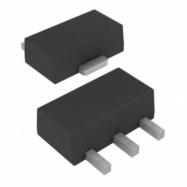
| 产品图片 |
|
| 产品型号 | LM340SX-5.0 |
| rohs | 含铅 / 不符合限制有害物质指令(RoHS)规范要求 |
| 产品系列 | - |
| 供应商器件封装 | DDPAK/TO-263-3 |
| 其它名称 | LM340SX-5.0TR |
| 包装 | 带卷 (TR) |
| 安装类型 | 表面贴装 |
| 封装/外壳 | TO-263-4,D²Pak(3 引线+接片),TO-263AA |
| 工作温度 | 0°C ~ 125°C |
| 标准包装 | 500 |
| 电压-跌落(典型值) | 2V @ 1A |
| 电压-输入 | 7.5 V ~ 35 V |
| 电压-输出 | 5V |
| 电流-输出 | 1A |
| 电流-限制(最小值) | - |
| 稳压器拓扑 | 正,固定式 |
| 稳压器数 | 1 |


PDF Datasheet 数据手册内容提取
Product Order Technical Tools & Support & Folder Now Documents Software Community LM340,LM340A,LM7805,LM7812,LM7815 SNOSBT0L–FEBRUARY2000–REVISEDSEPTEMBER2016 LM340, LM340A and LM7805 Family Wide V 1.5-A Fixed Voltage Regulators IN 1 Features 3 Description • OutputCurrentupto1.5A The LM340 and LM7805 Family monolithic 3-terminal 1 positive voltage regulators employ internal current- • AvailableinFixed5-V,12-V,and15-VOptions limiting, thermal shutdown and safe-area • OutputVoltageTolerancesof ±2%atTJ=25°C compensation,makingthemessentially indestructible. (LM340A) If adequate heat sinking is provided, they can deliver • LineRegulationof0.01%/Vofat1-ALoad over 1.5-A output current. They are intended as fixed voltage regulators in a wide range of applications (LM340A) including local (on-card) regulation for elimination of • LoadRegulationof0.3%/A(LM340A) noise and distribution problems associated with • InternalThermalOverload,Short-CircuitandSOA single-point regulation. In addition to use as fixed Protection voltage regulators, these devices can be used with external components to obtain adjustable output • AvailableinSpace-SavingSOT-223Package voltagesandcurrents. • OutputCapacitanceNotRequiredforStability Considerable effort was expended to make the entire 2 Applications series of regulators easy to use and minimize the numberofexternalcomponents.Itis not necessary to • IndustrialPowerSupplies bypass the output, although this does improve • SMPSPostRegulation transient response. Input bypassing is needed only if • HVACSystems the regulator is located far from the filter capacitor of thepowersupply. • ACInventors LM7805 is also available in a higher accuracy and • TestandMeasurementEquipment better performance version (LM340A). Refer to • BrushedandBrushlessDCMotorDrivers LM340A specifications in the LM340A Electrical • SolarEnergyStringInvertors Characterisitcstable. SPACE DeviceInformation(1) AvailablePackages PARTNUMBER PACKAGE BODYSIZE(NOM) Pin 1. Input DDPAK/TO-263(3) 10.18mm×8.41mm 2. Ground LM340x SOT-223(4) 6.50mm×3.50mm 3. Output 2 Tab/Case is Ground or Output 1 LM7805Family TO-220(3) 14.986mm×10.16mm TO-3(2) 38.94mmx25.40mm TO-3 TO-220 (1) For all available packages, see the orderable addendum at theendofthedatasheet. 1 2 3 FixedOutputVoltageRegulator TO-263 SOT-223 1 2 3 1 2 3 *Requirediftheregulatorislocatedfarfrom thepowersupplyfilter. **Althoughnooutputcapacitorisneeded forstability,itdoeshelptransientresponse. (Ifneeded,use0.1-μF,ceramicdisc). 1 An IMPORTANT NOTICE at the end of this data sheet addresses availability, warranty, changes, use in safety-critical applications, intellectualpropertymattersandotherimportantdisclaimers.PRODUCTIONDATA.
LM340,LM340A,LM7805,LM7812,LM7815 SNOSBT0L–FEBRUARY2000–REVISEDSEPTEMBER2016 www.ti.com Table of Contents 1 Features.................................................................. 1 7.3 FeatureDescription.................................................12 2 Applications........................................................... 1 7.4 DeviceFunctionalModes........................................12 3 Description............................................................. 1 8 ApplicationandImplementation........................ 13 4 RevisionHistory..................................................... 2 8.1 ApplicationInformation............................................13 8.2 TypicalApplications................................................14 5 PinConfigurationandFunctions......................... 3 8.3 SystemExamples...................................................15 6 Specifications......................................................... 4 9 PowerSupplyRecommendations...................... 17 6.1 AbsoluteMaximumRatings......................................4 10 Layout................................................................... 17 6.2 ESDRatings..............................................................4 6.3 RecommendedOperatingConditions.......................4 10.1 LayoutGuidelines.................................................17 6.4 ThermalInformation..................................................4 10.2 LayoutExample ...................................................17 6.5 LM340AElectricalCharacteristics, 10.3 HeatSinkingDDPAK/TO-263andSOT-223 PackageParts..........................................................18 V =5V,V =10V............................................................5 O I 11 DeviceandDocumentationSupport................. 20 6.6 LM340/LM7805ElectricalCharacteristics, V =5V,V =10V............................................................6 11.1 DocumentationSupport........................................20 O I 6.7 LM340/LM7812ElectricalCharacteristics, 11.2 RelatedLinks........................................................20 V =12V,V =19V..........................................................7 11.3 ReceivingNotificationofDocumentationUpdates20 O I 6.8 LM340/LM7815ElectricalCharacteristics, 11.4 CommunityResources..........................................20 VO=15V,VI=23V..........................................................8 11.5 Trademarks...........................................................20 6.9 TypicalCharacteristics..............................................9 11.6 ElectrostaticDischargeCaution............................20 7 DetailedDescription............................................ 12 11.7 Glossary................................................................20 7.1 Overview.................................................................12 12 Mechanical,Packaging,andOrderable 7.2 FunctionalBlockDiagram.......................................12 Information........................................................... 21 4 Revision History NOTE:Pagenumbersforpreviousrevisionsmaydifferfrompagenumbersinthecurrentversion. ChangesfromRevisionK(November2015)toRevisionL Page • ChangedpinoutnumberorderfortheTO-220andSOT-223packagesfrom:2,3,1to:1,2,3 .......................................... 1 ChangesfromRevisionJ(December2013)toRevisionK Page • AddedESDRatingstable,ThermalInformationtable,FeatureDescriptionsection,DeviceFunctionalModes, ApplicationandImplementationsection,PowerSupplyRecommendationssection,Layoutsection,Deviceand DocumentationSupportsection,andMechanical,Packaging,andOrderableInformationsection....................................... 1 • DeletedobsoleteLM140andLM7808Cdevicesfromthedatasheet................................................................................... 1 • ChangedFigure13captionfromLineRegulation140AK-5.0toLineRegulationLM340,.................................................. 11 • ChangedFigure14captionfromLineRegulation140AK-5.0toLineRegulationLM340,.................................................. 11 ChangesfromRevisionI(March2013)toRevisionJ Page • Changed0.5fromtyptomax................................................................................................................................................. 5 2 SubmitDocumentationFeedback Copyright©2000–2016,TexasInstrumentsIncorporated ProductFolderLinks:LM340 LM340A LM7805 LM7812 LM7815
LM340,LM340A,LM7805,LM7812,LM7815 www.ti.com SNOSBT0L–FEBRUARY2000–REVISEDSEPTEMBER2016 5 Pin Configuration and Functions LM7805andLM7812KTTPackage 3-PinDDPAK/TO-263 LM7805DCYPackage TopView 4-PinSOT-223 SideView LM340K-5.0NDSPackage 2-PinTO-3 TopView LM7805,LM7812,andLM7815NDEPackage 3-PinTO-220 TopView PinFunctions PIN I/O DESCRIPTION NAME NO. INPUT 1 I Inputvoltagepin GND 2 I/O Groundpin OUTPUT 3 O Outputvoltagepin Copyright©2000–2016,TexasInstrumentsIncorporated SubmitDocumentationFeedback 3 ProductFolderLinks:LM340 LM340A LM7805 LM7812 LM7815
LM340,LM340A,LM7805,LM7812,LM7815 SNOSBT0L–FEBRUARY2000–REVISEDSEPTEMBER2016 www.ti.com 6 Specifications 6.1 Absolute Maximum Ratings overoperatingfree-airtemperaturerange(unlessotherwisenoted)(1)(2) MIN MAX UNIT DCinputvoltage 35 V Internalpowerdissipation(3) InternallyLimited Maximumjunctiontemperature 150 °C TO-3package(NDS) 300 °C Leadtemperature(soldering,10sec.) Leadtemperature1,6mm(1/16in)fromcasefor10s 230 °C Storagetemperature −65 150 °C (1) StressesbeyondthoselistedunderAbsoluteMaximumRatingsmaycausepermanentdamagetothedevice.Thesearestressratings only,whichdonotimplyfunctionaloperationofthedeviceattheseoranyotherconditionsbeyondthoseindicatedunderRecommended OperatingConditions.Exposuretoabsolute-maximum-ratedconditionsforextendedperiodsmayaffectdevicereliability. (2) IfMilitary/Aerospacespecifieddevicesarerequired,pleasecontacttheTexasInstrumentsSalesOffice/Distributorsforavailabilityand specifications. (3) Themaximumallowablepowerdissipationatanyambienttemperatureisafunctionofthemaximumjunctiontemperatureforoperation (T =125°Cor150°C),thejunction-to-ambientthermalresistance(θ ),andtheambienttemperature(T ).P =(T − JMAX JA A DMAX JMAX T )/θ .Ifthisdissipationisexceeded,thedietemperaturerisesaboveT andtheelectricalspecificationsdonotapply.Ifthedie A JA JMAX temperaturerisesabove150°C,thedevicegoesintothermalshutdown.FortheTO-3package(NDS),thejunction-to-ambientthermal resistance(θ )is39°C/W.Whenusingaheatsink,θ isthesumofthe4°C/Wjunction-to-casethermalresistance(θ )oftheTO-3 JA JA JC packageandthecase-to-ambientthermalresistanceoftheheatsink.FortheTO-220package(NDE),θ is54°C/Wandθ is4°C/W. JA JC IfSOT-223isused,thejunction-to-ambientthermalresistanceis174°C/Wandcanbereducedbyaheatsink(seeApplicationsHintson heatsinking).IftheDDPAK\TO-263packageisused,thethermalresistancecanbereducedbyincreasingthePCBcopperarea thermallyconnectedtothepackage:Using0.5squareinchesofcopperarea,θ is50°C/W;with1squareinchofcopperarea,θ is JA JA 37°C/W;andwith1.6ormoreinchesofcopperarea,θ is32°C/W. JA 6.2 ESD Ratings VALUE UNIT V Electrostatic Human-bodymodel(HBM)(1) ±2000 V (ESD) discharge (1) ESDratingisbasedonthehuman-bodymodel,100pFdischargedthrough1.5kΩ. 6.3 Recommended Operating Conditions overoperatingfree-airtemperaturerange(unlessotherwisenoted) MIN MAX UNIT Temperature(T ) LM340A,LM340 0 125 °C A 6.4 Thermal Information LM340,LM7805Family NDE KTT DCY NDS THERMALMETRIC(1) UNIT (TO-220) (DDPAK/TO-263) (SOT-223) (TO-3) 3PINS 3PINS 4PINS 2PINS R Junction-to-ambientthermalresistance 23.9 44.8 62.1 39 °C/W θJA R Junction-to-case(top)thermalresistance 16.7 45.6 44 2 °C/W θJC(top) R Junction-to-boardthermalresistance 5.3 24.4 10.7 — °C/W θJB ψ Junction-to-topcharacterizationparameter 3.2 11.2 2.7 — °C/W JT ψ Junction-to-boardcharacterizationparameter 5.3 23.4 10.6 — °C/W JB R Junction-to-case(bottom)thermalresistance 1.7 1.5 — — °C/W θJC(bot) (1) Formoreinformationabouttraditionalandnewthermalmetrics,seetheSemiconductorandICPackageThermalMetricsapplication report. 4 SubmitDocumentationFeedback Copyright©2000–2016,TexasInstrumentsIncorporated ProductFolderLinks:LM340 LM340A LM7805 LM7812 LM7815
LM340,LM340A,LM7805,LM7812,LM7815 www.ti.com SNOSBT0L–FEBRUARY2000–REVISEDSEPTEMBER2016 6.5 LM340A Electrical Characteristics, V = 5 V, V = 10 V O I I =1A,0°C≤T ≤125°C(LM340A)unlessotherwisespecified(1) OUT J PARAMETER TESTCONDITIONS MIN TYP MAX UNIT TJ=25°C 4.9 5 5.1 V VO Outputvoltage PD≤15W,5mA≤IO≤1A 4.8 5.2 V 7.5V≤V ≤20V IN 7.5V≤VIN≤20 TJ=25°C 3 10 mV V Overtemperature,IO=500mA 10 mV ΔVO Lineregulation TJ=25°C 4 mV 8V≤VIN≤12V Overtemperature 12 mV 5mA≤IO≤1.5A 10 25 mV TJ=25°C ΔVO Loadregulation 250mA≤IO≤750mA 15 mV Overtemperature,5mA≤IO≤1A 25 mV TJ=25°C 6 mA IQ Quiescentcurrent Overtemperature 6.5 mA TJ=25°C,IO=1A 0.8 mA 7.5V≤V ≤20V IN Quiescentcurrent ΔIQ change Overtemperature,5mA≤IO≤1A 0.5 mA Overtemperature,IO=500mA 0.8 mA 8V≤V ≤25V IN VN Outputnoisevoltage TA=25°C,10Hz≤f≤100kHz 40 μV f=120Hz TJ=25°C,,IO=1A 68 80 dB Ripplerejection 8 V≤VIN ≤ 18 68 V Overtemperature,IO=500mA dB Dropoutvoltage TJ=25°C,IO=1A 2 V Outputresistance f=1kHz 8 mΩ RO Short-circuitcurrent TJ=25°C 2.1 A Peakoutputcurrent TJ=25°C 2.4 A AverageTCofVO Min,TJ=0°C,IO=5mA −0.6 mV/°C Inputvoltagerequiredto VIN maintainlineregulation TJ=25°C 7.5 V (1) Allcharacteristicsaremeasuredwitha0.22-μFcapacitorfrominputtogroundanda0.1-μFcapacitorfromoutputtoground.All characteristicsexceptnoisevoltageandripplerejectionratioaremeasuredusingpulsetechniques(t ≤10ms,dutycycle≤5%). w Outputvoltagechangesduetochangesininternaltemperaturemustbetakenintoaccountseparately. Copyright©2000–2016,TexasInstrumentsIncorporated SubmitDocumentationFeedback 5 ProductFolderLinks:LM340 LM340A LM7805 LM7812 LM7815
LM340,LM340A,LM7805,LM7812,LM7815 SNOSBT0L–FEBRUARY2000–REVISEDSEPTEMBER2016 www.ti.com 6.6 LM340 / LM7805 Electrical Characteristics, V = 5 V, V = 10 V O I 0°C≤T ≤125°Cunlessotherwisespecified(1) J PARAMETER TESTCONDITIONS MIN TYP MAX UNIT TJ=25°C,5mA≤IO≤1A 4.8 5 5.2 V VO Outputvoltage PD≤15W,5mA≤IO≤1A 4.75 5.25 V 7.5V≤V ≤20V IN TJ=25°C 3 50 mV 7V≤V ≤25V IN IO=500mA Overtemperature 50 mV 8V≤V ≤20V IN ΔVO Lineregulation TJ=25°C 50 mV 7.5V≤V ≤20V IN IO≤1A Overtemperature 25 mV 8V≤V ≤12V IN 5mA≤IO≤1.5A 10 50 mV TJ=25°C ΔVO Loadregulation 250mA≤IO≤750mA 25 mV Overtemperature,5mA≤IO≤1A 50 mV TJ=25°C 8 mA IQ Quiescentcurrent IO≤1A Overtemperature 8.5 mA 0°C≤TJ≤125°C,5mA≤IO≤1A 0.5 mA ΔIQ Quiescentcurrentchange TJ=25°C,IO≤1A 1 mA 7V≤VIN≤20V Overtemperature,IO≤500 1 mA mA VN Outputnoisevoltage TA=25°C,10Hz≤f≤100kHz 40 μV f=120Hz TJ=25°C,IO≤1A 62 80 dB Ripplerejection 8V≤VIN≤18V OmvAertemperature,IO≤500 62 dB Dropoutvoltage TJ=25°C,IO=1A 2 V Outputresistance f=1kHz 8 mΩ RO Short-circuitcurrent TJ=25°C 2.1 A Peakoutputcurrent TJ=25°C 2.4 A AverageTCofVOUT Overtemperature,IO=5mA −0.6 mV/°C VIN Inputvoltagerequiredto TJ=25°C,IO≤1A 7.5 V maintainlineregulation (1) Allcharacteristicsaremeasuredwitha0.22-μFcapacitorfrominputtogroundanda0.1-μFcapacitorfromoutputtoground.All characteristicsexceptnoisevoltageandripplerejectionratioaremeasuredusingpulsetechniques(t ≤10ms,dutycycle≤5%). w Outputvoltagechangesduetochangesininternaltemperaturemustbetakenintoaccountseparately. 6 SubmitDocumentationFeedback Copyright©2000–2016,TexasInstrumentsIncorporated ProductFolderLinks:LM340 LM340A LM7805 LM7812 LM7815
LM340,LM340A,LM7805,LM7812,LM7815 www.ti.com SNOSBT0L–FEBRUARY2000–REVISEDSEPTEMBER2016 6.7 LM340 / LM7812 Electrical Characteristics, V = 12 V, V = 19 V O I 0°C≤T ≤125°Cunlessotherwisespecified(1) J PARAMETER TESTCONDITIONS MIN TYP MAX UNIT TJ=25°C,5mA≤IO≤1A 11.5 12 12.5 V VO Outputvoltage PD≤15W,5mA≤IO≤1A 11.4 12.6 V 14.5V≤V ≤27V IN TJ=25°C 4 120 mV 14.5V≤V ≤30V IN IO=500mA Overtemperature 120 mV 15V≤V ≤27V IN ΔVO Lineregulation TJ=25°C 120 mV 14.6V≤V ≤27V IN IO≤1A Overtemperature 60 mV 16V≤V ≤22V IN 5mA≤IO≤1.5A 12 120 mV TJ=25°C ΔVO Loadregulation 250mA≤IO≤750mA 60 mV Overtemperature,5mA≤IO≤1A 120 mV TJ=25°C 8 mA IQ Quiescentcurrent IO≤1A Overtemperature 8.5 mA 5mA≤IO≤1A 0.5 mA TJ=25°C,IO≤1A 1 mA ΔIQ Quiescentcurrentchange 14.8V≤VIN≤27V Overtemperature,IO≤500mA 1 mA 14.5V≤V ≤30V IN VN Outputnoisevoltage TA=25°C,10Hz≤f≤100kHz 75 μV f=120Hz TJ=25°C,IO≤1A 55 72 dB Ripplerejection 15 V ≤ VIN ≤ 25 Overtemperature,IO≤500 55 dB V mA, Dropoutvoltage TJ=25°C,IO=1A 2 V Outputresistance f=1kHz 18 mΩ RO Short-circuitcurrent TJ=25°C 1.5 A Peakoutputcurrent TJ=25°C 2.4 A AverageTCofVOUT Overtemperature,IO=5mA −1.5 mV/°C VIN Inputvoltagerequiredto TJ=25°C,IO≤1A 14.6 V maintainlineregulation (1) Allcharacteristicsaremeasuredwitha0.22-μFcapacitorfrominputtogroundanda0.1-μFcapacitorfromoutputtoground.All characteristicsexceptnoisevoltageandripplerejectionratioaremeasuredusingpulsetechniques(t ≤10ms,dutycycle≤5%). w Outputvoltagechangesduetochangesininternaltemperaturemustbetakenintoaccountseparately. Copyright©2000–2016,TexasInstrumentsIncorporated SubmitDocumentationFeedback 7 ProductFolderLinks:LM340 LM340A LM7805 LM7812 LM7815
LM340,LM340A,LM7805,LM7812,LM7815 SNOSBT0L–FEBRUARY2000–REVISEDSEPTEMBER2016 www.ti.com 6.8 LM340 / LM7815 Electrical Characteristics, V = 15 V, V = 23 V O I 0°C≤T ≤125°Cunlessotherwisespecified(1) J PARAMETER TESTCONDITIONS MIN TYP MAX UNIT TJ=25°C,5mA≤IO≤1A 14.4 15 15.6 V VO Outputvoltage PD≤15W,5mA≤IO≤1A 14.25 15.75 V 17.5V≤V ≤30V IN TJ=25°C 4 150 mV 17.5V≤V ≤30V IN IO=500mA Overtemperature 150 mV 18.5V≤V ≤30V IN ΔVO Lineregulation TJ=25°C 150 mV 17.7V≤V ≤30V IN IO≤1A Overtemperature 75 mV 20V≤V ≤26V IN 5mA≤IO≤1.5A 12 150 mV TJ=25°C ΔVO Loadregulation 250mA≤IO≤750mA 75 mV Overtemperature,5mA≤IO≤1A, 150 mV TJ=25°C 8 mA IQ Quiescentcurrent IO≤1A Overtemperature 8.5 mA 5mA≤IO≤1A 0.5 mA TJ=25°C,IO≤1A 1 mA ΔIQ Quiescentcurrentchange 17.9V≤VIN≤30V Overtemperature,IO≤500mA 1 mA 17.5V≤V ≤30V IN VN Outputnoisevoltage TA=25°C,10Hz≤f≤100kHz 90 μV f=120Hz TJ=25°C,IO≤1A 54 70 dB Ripplerejection 18.5 V ≤ VIN ≤ Overtemperature,IO≤500 54 dB 28.5V mA, Dropoutvoltage TJ=25°C,IO=1A 2 V Outputresistance f=1kHz 19 mΩ RO Short-circuitcurrent TJ=25°C 1.2 A Peakoutputcurrent TJ=25°C 2.4 A AverageTCofVOUT Overtemperature,IO=5mA −1.8 mV/°C VIN Inputvoltagerequiredto TJ=25°C,IO≤1A 17.7 V maintainlineregulation (1) Allcharacteristicsaremeasuredwitha0.22-μFcapacitorfrominputtogroundanda0.1-μFcapacitorfromoutputtoground.All characteristicsexceptnoisevoltageandripplerejectionratioaremeasuredusingpulsetechniques(t ≤10ms,dutycycle≤5%). w Outputvoltagechangesduetochangesininternaltemperaturemustbetakenintoaccountseparately. 8 SubmitDocumentationFeedback Copyright©2000–2016,TexasInstrumentsIncorporated ProductFolderLinks:LM340 LM340A LM7805 LM7812 LM7815
LM340,LM340A,LM7805,LM7812,LM7815 www.ti.com SNOSBT0L–FEBRUARY2000–REVISEDSEPTEMBER2016 6.9 Typical Characteristics Figure1.MaximumAveragePowerDissipation Figure2.MaximumAveragePowerDissipation ShadedareareferstoLM340A/LM340,LM7805,LM7812and LM7815. Figure3.MaximumPowerDissipation(DDPAK/TO-263) Figure4.OutputVoltage(Normalizedto1VatT =25°C) J Figure5.RippleRejection Figure6.RippleRejection Copyright©2000–2016,TexasInstrumentsIncorporated SubmitDocumentationFeedback 9 ProductFolderLinks:LM340 LM340A LM7805 LM7812 LM7815
LM340,LM340A,LM7805,LM7812,LM7815 SNOSBT0L–FEBRUARY2000–REVISEDSEPTEMBER2016 www.ti.com Typical Characteristics (continued) Figure7.OutputImpedance Figure8.DropoutCharacteristics ShadedareareferstoLM340A/LM340,LM7805,LM7812,and LM7815. Figure9.QuiescentCurrent Figure10.PeakOutputCurrent ShadedareareferstoLM340A/LM340,LM7805,LM7812,and LM7815. Figure11.DropoutVoltage Figure12.QuiescentCurrent 10 SubmitDocumentationFeedback Copyright©2000–2016,TexasInstrumentsIncorporated ProductFolderLinks:LM340 LM340A LM7805 LM7812 LM7815
LM340,LM340A,LM7805,LM7812,LM7815 www.ti.com SNOSBT0L–FEBRUARY2000–REVISEDSEPTEMBER2016 Typical Characteristics (continued) IOUT=1A,TA=25°C VIN=10V,TA=25°C Figure13.LineRegulationLM340 Figure14.LineRegulationLM340 Copyright©2000–2016,TexasInstrumentsIncorporated SubmitDocumentationFeedback 11 ProductFolderLinks:LM340 LM340A LM7805 LM7812 LM7815
LM340,LM340A,LM7805,LM7812,LM7815 SNOSBT0L–FEBRUARY2000–REVISEDSEPTEMBER2016 www.ti.com 7 Detailed Description 7.1 Overview TheLM340andLM7805devicesareafamilyoffixedoutputpositivevoltage regulators with outputs ranging from 3 V to 15 V. They accept up to 35 V of input voltage and with proper heat dissipation can provide over 1.5 A of current. With a combination of current limiting, thermal shutdown, and safe area protection, these regulators eliminate any concern of damage. These features paired with excellent line and load regulation make the LM340 and LM7805 Family versatile solutions to a wide range of power management designs. Although the LM340 and LM7805 Family were designed primarily as fixed-voltage regulators, these devices can be used with external componentforadjustablevoltageandcurrent. 7.2 Functional Block Diagram 7.3 Feature Description 7.3.1 OutputCurrent With proper considerations, the LM340 and LM7805 Family can exceed 1.5-A output current. Depending on the desired package option, the effective junction-to-ambient thermal resistance can be reduced through heat sinking,allowingmorepowertobedissipatedinthedevice. 7.3.2 CurrentLimitingFeature In the event of a short circuit at the output of the regulator, each device has an internal current limit to protect it fromdamage.ThetypicalcurrentlimitsfortheLM340andLM7805Familyis2.4A. 7.3.3 ThermalShutdown Each package type employs internal current limiting and thermal shutdown to provide safe operation area protection.Ifthejunctiontemperatureisallowedtoriseto150°C,thedevicewillgointothermalshutdown. 7.4 Device Functional Modes Therearenofunctionalmodesforthisdevice. 12 SubmitDocumentationFeedback Copyright©2000–2016,TexasInstrumentsIncorporated ProductFolderLinks:LM340 LM340A LM7805 LM7812 LM7815
LM340,LM340A,LM7805,LM7812,LM7815 www.ti.com SNOSBT0L–FEBRUARY2000–REVISEDSEPTEMBER2016 8 Application and Implementation NOTE Information in the following applications sections is not part of the TI component specification, and TI does not warrant its accuracy or completeness. TI’s customers are responsible for determining suitability of components for their purposes. Customers should validateandtesttheirdesignimplementationtoconfirmsystemfunctionality. 8.1 Application Information The LM340x and LM7805 series is designed with thermal protection, output short-circuit protection, and output transistor safe area protection. However, as with any IC regulator, it becomes necessary to take precautions to assure that the regulator is not inadvertently damaged. The following describes possible misapplications and methodstopreventdamagetotheregulator. 8.1.1 ShortingtheRegulatorInput When using large capacitors at the output of these regulators, a protection diode connected input to output (Figure 15) may be required if the input is shorted to ground. Without the protection diode, an input short causes the input to rapidly approach ground potential, while the output remains near the initial V because of the OUT stored charge in the large output capacitor. The capacitor will then discharge through a large internal input to output diode and parasitic transistors. If the energy released by the capacitor is large enough, this diode, low current metal, and the regulator are destroyed. The fast diode in Figure 15 shunts most of the capacitors dischargecurrentaroundtheregulator.Generally no protection diode is required for values of output capacitance ≤10 μF. 8.1.2 RaisingtheOutputVoltageAbovetheInputVoltage Because the output of the device does not sink current, forcing the output high can cause damage to internal low currentpathsinamannersimilartothatjustdescribedinShortingtheRegulatorInput. 8.1.3 RegulatorFloatingGround When the ground pin alone becomes disconnected, the output approaches the unregulated input, causing possible damage to other circuits connected to V . If ground is reconnected with power ON, damage may also OUT occur to the regulator. This fault is most likely to occur when plugging in regulators or modules with on card regulators into powered up sockets. The power must be turned off first, the thermal limit ceases operating, or the groundmustbeconnectedfirstifpowermustbelefton.SeeFigure16. 8.1.4 TransientVoltages If transients exceed the maximum rated input voltage of the device, or reach more than 0.8 V below ground and have sufficient energy, they will damage the regulator. The solution is to use a large input capacitor, a series inputbreakdowndiode,achoke,atransientsuppressororacombinationofthese. Figure15. InputShort Copyright©2000–2016,TexasInstrumentsIncorporated SubmitDocumentationFeedback 13 ProductFolderLinks:LM340 LM340A LM7805 LM7812 LM7815
LM340,LM340A,LM7805,LM7812,LM7815 SNOSBT0L–FEBRUARY2000–REVISEDSEPTEMBER2016 www.ti.com Application Information (continued) Figure16. RegulatorFloatingGround Figure17. Transients When a value for θ is found, a heat sink must be selected that has a value that is less than or equal to this (H–A) number. θ is specified numerically by the heat sink manufacturer in this catalog or shown in a curve that plots (H–A) temperaturerisevspowerdissipationfortheheatsink. 8.2 Typical Applications 8.2.1 FixedOutputVoltageRegulator The LM340x and LM7805 Family devices are primarily designed to provide fixed output voltage regulation. The simplestimplementationofLM340xandLM7805FamilyisshowninFigure18. *Requirediftheregulatorislocatedfarfromthepowersupplyfilter. **Althoughnooutputcapacitorisneededforstability,itdoeshelptransientresponse.(Ifneeded,use0.1-μF,ceramic disc). Figure18. FixedOutputVoltageRegulator 8.2.1.1 DesignRequirements The device component count is very minimal. Although not required, TI recommends employing bypass capacitors at the output for optimum stability and transient response. These capacitors must be placed as close as possible to the regulator. If the device is located more than 6 inches from the power supply filter, it is required toemployinputcapacitor. 14 SubmitDocumentationFeedback Copyright©2000–2016,TexasInstrumentsIncorporated ProductFolderLinks:LM340 LM340A LM7805 LM7812 LM7815
LM340,LM340A,LM7805,LM7812,LM7815 www.ti.com SNOSBT0L–FEBRUARY2000–REVISEDSEPTEMBER2016 Typical Applications (continued) 8.2.1.2 DetailedDesignProcedure The output voltage is set based on the device variant. LM340x and LM7805 Family are available in 5-V, 12-V and15-Vregulatoroptions. 8.2.1.3 ApplicationCurve Figure19. V vsV ,V =5V OUT IN OUT 8.3 System Examples I =V2–3/R1+I OUT Q V =5V+(5V/R1+I )R25V/R1>3I , OUT Q Q ΔI =1.3mAoverlineandloadchanges. Q loadregulation(L)≈[(R1+R2)/R1](L ofLM340-5). r r Figure20.CurrentRegulator Figure21.AdjustableOutputRegulator INPUT OUTPUT INPUT OUTPUT VI VO VI VO 0.22 PF GND 0.1 PF GND 0.22 PF 0.1 PF Figure22.HighInputVoltageCircuitWithSeries Figure23.HighInputVoltageCircuit Resistor implementationWithTransistor Copyright©2000–2016,TexasInstrumentsIncorporated SubmitDocumentationFeedback 15 ProductFolderLinks:LM340 LM340A LM7805 LM7812 LM7815
LM340,LM340A,LM7805,LM7812,LM7815 SNOSBT0L–FEBRUARY2000–REVISEDSEPTEMBER2016 www.ti.com System Examples (continued) 2NQ61133 IQ1 IN RSC 2NQ61132 VI Q2 R1 2N6124 3.0: IREG OUTPUT IO MAX VO INPUT INPUT OUT 0.22 PF GND 0.1 PF R1 OUTPUT 3.0: 0.22 PF GND 0.1 PF β(Q1)≥I /I R =0.8/I OMax REGMax SC SC R1=0.9/I =β V /I –I R1=βV /I (β+1)–I REG (Q1) BE(Q1) REGMax(β+1) OMax BE(Q1) REGMax OMax Figure24.HighCurrentVoltageRegulator Figure25.HighOutputCurrentWithShort-Circuit Protection INPUT OUTPUT LM340 + OUT + + GND 0.1 PF INPUT OUTPUT LM79xx + + GND 0.1 PF - OUT Figure26.LM340UsedWithNegativeRegulatorLM79xx 16 SubmitDocumentationFeedback Copyright©2000–2016,TexasInstrumentsIncorporated ProductFolderLinks:LM340 LM340A LM7805 LM7812 LM7815
LM340,LM340A,LM7805,LM7812,LM7815 www.ti.com SNOSBT0L–FEBRUARY2000–REVISEDSEPTEMBER2016 9 Power Supply Recommendations The LM340 is designed to operate from a wide input voltage up to 35 V. Please refer to electrical characteristics tables for the minimum input voltage required for line/load regulation. If the device is more than six inches from theinputfiltercapacitors,aninputbypasscapacitor,0.1 μForgreater,ofanytypeisneededforstability. 10 Layout 10.1 Layout Guidelines Some layout guidelines must be followed to ensure proper regulation of the output voltage with minimum noise. Traces carrying the load current must be wide to reduce the amount of parasitic trace inductance. To improve PSRR, a bypass capacitor can be placed at the OUTPUT pin and must be placed as close as possible to the IC. All that is required for the typical fixed output regulator application circuit is the LM340x/LM7805 Family IC and a 0.22-µF input capacitor if the regulator is placed far from the power supply filter. A 0.1-µF output capacitor is recommended to help with transient response. In cases when VIN shorts to ground, an external diode must be placedfromVOUTtoVINtodivertthesurgecurrentfromtheoutputcapacitorandprotecttheIC. 10.2 Layout Example Figure27. LayoutExampleDDPAK Copyright©2000–2016,TexasInstrumentsIncorporated SubmitDocumentationFeedback 17 ProductFolderLinks:LM340 LM340A LM7805 LM7812 LM7815
LM340,LM340A,LM7805,LM7812,LM7815 SNOSBT0L–FEBRUARY2000–REVISEDSEPTEMBER2016 www.ti.com Layout Example (continued) Figure28. LayoutExampleSOT-223 10.3 Heat Sinking DDPAK/TO-263 and SOT-223 Package Parts Both the DDPAK/TO-263 (KTT) and SOT-223 (DCY) packages use a copper plane on the PCB and the PCB itselfasaheatsink.TooptimizetheheatsinkingabilityoftheplaneandPCB,solderthetaboftheplane. Figure 29 shows for the DDPAK/TO-263 the measured values of θ for different copper area sizes using a (J–A) typicalPCBwith1-ozcopper andnosoldermaskoverthecopperareausedforheatsinking. Figure29. θ vsCopper(1Ounce)AreafortheDDPAK/TO-263Package (J–A) 18 SubmitDocumentationFeedback Copyright©2000–2016,TexasInstrumentsIncorporated ProductFolderLinks:LM340 LM340A LM7805 LM7812 LM7815
LM340,LM340A,LM7805,LM7812,LM7815 www.ti.com SNOSBT0L–FEBRUARY2000–REVISEDSEPTEMBER2016 Heat Sinking DDPAK/TO-263 and SOT-223 Package Parts (continued) As shown in Figure 29, increasing the copper area beyond 1 square inch produces very little improvement. It should also be observed that the minimum value of θ for the DDPAK/TO-263 package mounted to a PCB is (J–A) 32°C/W. As a design aid, Figure 30 shows the maximum allowable power dissipation compared to ambient temperature fortheDDPAK/TO-263device(assuming θ is35°C/Wandthemaximumjunctiontemperatureis125°C). (J–A) Figure30. MaximumPowerDissipationvsT fortheDDPAK/TO-263Package AMB Figure 31 and Figure 32 show the information for the SOT-223 package. Figure 31 assumes a θ of 74°C/W (J–A) for1-oz.copperand51°C/Wfor2-oz.copperandamaximumjunctiontemperatureof125°C. Figure31.θ vsCopper(2Ounce)Area Figure32.MaximumPowerDissipationvs (J–A) fortheSOT-223Package T fortheSOT-223Package AMB See AN-1028 LMX2370 PLLatinum Dual Freq Synth for RF Pers Comm LMX2370 2.5GHz/1.2GHz (SNVA036) forpowerenhancementtechniquestobeusedwiththeSOT-223package. Copyright©2000–2016,TexasInstrumentsIncorporated SubmitDocumentationFeedback 19 ProductFolderLinks:LM340 LM340A LM7805 LM7812 LM7815
LM340,LM340A,LM7805,LM7812,LM7815 SNOSBT0L–FEBRUARY2000–REVISEDSEPTEMBER2016 www.ti.com 11 Device and Documentation Support 11.1 Documentation Support 11.1.1 RelatedDocumentation Forrelateddocumentation,seethefollowing: • AN-1028LMX2370PLLatinumDualFreqSynthforRFPersCommLMX23702.5GHz/1.2GHz (SNVA036) • LM140KSeries3-TerminalPositiveRegulators (SNVS994) 11.2 Related Links The table below lists quick access links. Categories include technical documents, support and community resources,toolsandsoftware,andquickaccesstosampleorbuy. Table1.RelatedLinks TECHNICAL TOOLS& SUPPORT& PARTS PRODUCTFOLDER SAMPLE&BUY DOCUMENTS SOFTWARE COMMUNITY LM340 Clickhere Clickhere Clickhere Clickhere Clickhere LM340A Clickhere Clickhere Clickhere Clickhere Clickhere LM7805 Clickhere Clickhere Clickhere Clickhere Clickhere LM7812 Clickhere Clickhere Clickhere Clickhere Clickhere LM7815 Clickhere Clickhere Clickhere Clickhere Clickhere 11.3 Receiving Notification of Documentation Updates To receive notification of documentation updates, navigate to the device product folder on ti.com. In the upper right corner, click on Alert me to register and receive a weekly digest of any product information that has changed.Forchangedetails,reviewtherevisionhistoryincludedinanyreviseddocument. 11.4 Community Resources The following links connect to TI community resources. Linked contents are provided "AS IS" by the respective contributors. They do not constitute TI specifications and do not necessarily reflect TI's views; see TI's Terms of Use. TIE2E™OnlineCommunity TI'sEngineer-to-Engineer(E2E)Community.Createdtofostercollaboration amongengineers.Ate2e.ti.com,youcanaskquestions,shareknowledge,exploreideasandhelp solveproblemswithfellowengineers. DesignSupport TI'sDesignSupport QuicklyfindhelpfulE2Eforumsalongwithdesignsupporttoolsand contactinformationfortechnicalsupport. 11.5 Trademarks E2EisatrademarkofTexasInstruments. Allothertrademarksarethepropertyoftheirrespectiveowners. 11.6 Electrostatic Discharge Caution Thesedeviceshavelimitedbuilt-inESDprotection.Theleadsshouldbeshortedtogetherorthedeviceplacedinconductivefoam duringstorageorhandlingtopreventelectrostaticdamagetotheMOSgates. 11.7 Glossary SLYZ022—TIGlossary. Thisglossarylistsandexplainsterms,acronyms,anddefinitions. 20 SubmitDocumentationFeedback Copyright©2000–2016,TexasInstrumentsIncorporated ProductFolderLinks:LM340 LM340A LM7805 LM7812 LM7815
LM340,LM340A,LM7805,LM7812,LM7815 www.ti.com SNOSBT0L–FEBRUARY2000–REVISEDSEPTEMBER2016 12 Mechanical, Packaging, and Orderable Information The following pages include mechanical, packaging, and orderable information. This information is the most current data available for the designated devices. This data is subject to change without notice and revision of thisdocument.Forbrowser-basedversionsofthisdatasheet,refertotheleft-handnavigation. Copyright©2000–2016,TexasInstrumentsIncorporated SubmitDocumentationFeedback 21 ProductFolderLinks:LM340 LM340A LM7805 LM7812 LM7815
PACKAGE OPTION ADDENDUM www.ti.com 6-Feb-2020 PACKAGING INFORMATION Orderable Device Status Package Type Package Pins Package Eco Plan Lead/Ball Finish MSL Peak Temp Op Temp (°C) Device Marking Samples (1) Drawing Qty (2) (6) (3) (4/5) LM340AT-5.0 NRND TO-220 NDE 3 45 TBD Call TI Call TI 0 to 70 LM340AT 5.0 P+ LM340AT-5.0/NOPB ACTIVE TO-220 NDE 3 45 Pb-Free (RoHS SN Level-1-NA-UNLIM 0 to 125 LM340AT Exempt) 5.0 P+ LM340K-5.0 ACTIVE TO-3 NDS 2 50 TBD Call TI Call TI 0 to 125 LM340K -5.0 7805P+ LM340K-5.0/NOPB ACTIVE TO-3 NDS 2 50 Green (RoHS Call TI Level-1-NA-UNLIM 0 to 125 LM340K & no Sb/Br) -5.0 7805P+ LM340MP-5.0 NRND SOT-223 DCY 4 1000 TBD Call TI Call TI 0 to 70 N00A LM340MP-5.0/NOPB ACTIVE SOT-223 DCY 4 1000 Green (RoHS SN Level-1-260C-UNLIM 0 to 125 N00A & no Sb/Br) LM340MPX-5.0/NOPB ACTIVE SOT-223 DCY 4 2000 Green (RoHS SN Level-1-260C-UNLIM 0 to 125 N00A & no Sb/Br) LM340S-12/NOPB ACTIVE DDPAK/ KTT 3 45 Pb-Free (RoHS SN Level-3-245C-168 HR 0 to 125 LM340S TO-263 Exempt) -12 P+ LM340S-5.0 NRND DDPAK/ KTT 3 45 TBD Call TI Call TI 0 to 70 LM340S TO-263 -5.0 P+ LM340S-5.0/NOPB ACTIVE DDPAK/ KTT 3 45 Pb-Free (RoHS SN Level-3-245C-168 HR 0 to 125 LM340S TO-263 Exempt) -5.0 P+ LM340SX-12/NOPB ACTIVE DDPAK/ KTT 3 500 Pb-Free (RoHS SN Level-3-245C-168 HR 0 to 125 LM340S TO-263 Exempt) -12 P+ LM340SX-5.0 NRND DDPAK/ KTT 3 500 TBD Call TI Call TI 0 to 70 LM340S TO-263 -5.0 P+ LM340SX-5.0/NOPB ACTIVE DDPAK/ KTT 3 500 Pb-Free (RoHS SN Level-3-245C-168 HR 0 to 125 LM340S TO-263 Exempt) -5.0 P+ LM340T-12 NRND TO-220 NDE 3 45 TBD Call TI Call TI 0 to 70 LM340T12 7812 P+ LM340T-12/NOPB ACTIVE TO-220 NDE 3 45 Green (RoHS SN Level-1-NA-UNLIM LM340T12 & no Sb/Br) 7812 P+ LM340T-15 NRND TO-220 NDE 3 45 TBD Call TI Call TI 0 to 70 LM340T15 7815 P+ LM340T-15/NOPB ACTIVE TO-220 NDE 3 45 Green (RoHS SN Level-1-NA-UNLIM 0 to 125 LM340T15 & no Sb/Br) 7815 P+ LM340T-5.0 NRND TO-220 NDE 3 45 TBD Call TI Call TI 0 to 70 LM340T5 Addendum-Page 1
PACKAGE OPTION ADDENDUM www.ti.com 6-Feb-2020 Orderable Device Status Package Type Package Pins Package Eco Plan Lead/Ball Finish MSL Peak Temp Op Temp (°C) Device Marking Samples (1) Drawing Qty (2) (6) (3) (4/5) 7805 P+ LM340T-5.0/LF01 ACTIVE TO-220 NDG 3 45 Pb-Free (RoHS SN Level-4-260C-72 HR 0 to 125 LM340T5 Exempt) 7805 P+ LM340T-5.0/NOPB ACTIVE TO-220 NDE 3 45 Pb-Free (RoHS SN Level-1-NA-UNLIM 0 to 125 LM340T5 Exempt) 7805 P+ LM7805CT NRND TO-220 NDE 3 45 TBD Call TI Call TI 0 to 125 LM340T5 7805 P+ LM7805CT/NOPB ACTIVE TO-220 NDE 3 45 Pb-Free (RoHS SN Level-1-NA-UNLIM 0 to 125 LM340T5 Exempt) 7805 P+ LM7805MP/NOPB ACTIVE SOT-223 DCY 4 1000 Green (RoHS SN Level-1-260C-UNLIM 0 to 125 N00A & no Sb/Br) LM7805MPX/NOPB ACTIVE SOT-223 DCY 4 2000 Green (RoHS SN Level-1-260C-UNLIM 0 to 125 N00A & no Sb/Br) LM7805S/NOPB ACTIVE DDPAK/ KTT 3 45 Pb-Free (RoHS SN Level-3-245C-168 HR 0 to 125 LM340S TO-263 Exempt) -5.0 P+ LM7805SX/NOPB ACTIVE DDPAK/ KTT 3 500 Pb-Free (RoHS SN Level-3-245C-168 HR 0 to 125 LM340S TO-263 Exempt) -5.0 P+ LM7812CT/NOPB ACTIVE TO-220 NDE 3 45 Green (RoHS SN Level-1-NA-UNLIM -40 to 125 LM340T12 & no Sb/Br) 7812 P+ LM7812S/NOPB ACTIVE DDPAK/ KTT 3 45 Pb-Free (RoHS SN Level-3-245C-168 HR 0 to 125 LM340S TO-263 Exempt) -12 P+ LM7812SX/NOPB ACTIVE DDPAK/ KTT 3 500 Pb-Free (RoHS SN Level-3-245C-168 HR 0 to 125 LM340S TO-263 Exempt) -12 P+ LM7815CT/NOPB ACTIVE TO-220 NDE 3 45 Green (RoHS SN Level-1-NA-UNLIM 0 to 125 LM340T15 & no Sb/Br) 7815 P+ LM78S40CN/NOPB ACTIVE PDIP NFG 16 25 Pb-Free SN Level-1-NA-UNLIM 0 to 70 LM78S40CN (RoHS) LM78S40N/NOPB ACTIVE PDIP NFG 16 25 Pb-Free SN Level-1-NA-UNLIM 0 to 125 LM78S40N (RoHS) (1) The marketing status values are defined as follows: ACTIVE: Product device recommended for new designs. LIFEBUY: TI has announced that the device will be discontinued, and a lifetime-buy period is in effect. NRND: Not recommended for new designs. Device is in production to support existing customers, but TI does not recommend using this part in a new design. PREVIEW: Device has been announced but is not in production. Samples may or may not be available. OBSOLETE: TI has discontinued the production of the device. Addendum-Page 2
PACKAGE OPTION ADDENDUM www.ti.com 6-Feb-2020 (2) RoHS: TI defines "RoHS" to mean semiconductor products that are compliant with the current EU RoHS requirements for all 10 RoHS substances, including the requirement that RoHS substance do not exceed 0.1% by weight in homogeneous materials. Where designed to be soldered at high temperatures, "RoHS" products are suitable for use in specified lead-free processes. TI may reference these types of products as "Pb-Free". RoHS Exempt: TI defines "RoHS Exempt" to mean products that contain lead but are compliant with EU RoHS pursuant to a specific EU RoHS exemption. Green: TI defines "Green" to mean the content of Chlorine (Cl) and Bromine (Br) based flame retardants meet JS709B low halogen requirements of <=1000ppm threshold. Antimony trioxide based flame retardants must also meet the <=1000ppm threshold requirement. (3) MSL, Peak Temp. - The Moisture Sensitivity Level rating according to the JEDEC industry standard classifications, and peak solder temperature. (4) There may be additional marking, which relates to the logo, the lot trace code information, or the environmental category on the device. (5) Multiple Device Markings will be inside parentheses. Only one Device Marking contained in parentheses and separated by a "~" will appear on a device. If a line is indented then it is a continuation of the previous line and the two combined represent the entire Device Marking for that device. (6) Lead/Ball Finish - Orderable Devices may have multiple material finish options. Finish options are separated by a vertical ruled line. Lead/Ball Finish values may wrap to two lines if the finish value exceeds the maximum column width. Important Information and Disclaimer:The information provided on this page represents TI's knowledge and belief as of the date that it is provided. TI bases its knowledge and belief on information provided by third parties, and makes no representation or warranty as to the accuracy of such information. Efforts are underway to better integrate information from third parties. TI has taken and continues to take reasonable steps to provide representative and accurate information but may not have conducted destructive testing or chemical analysis on incoming materials and chemicals. TI and TI suppliers consider certain information to be proprietary, and thus CAS numbers and other limited information may not be available for release. In no event shall TI's liability arising out of such information exceed the total purchase price of the TI part(s) at issue in this document sold by TI to Customer on an annual basis. Addendum-Page 3
PACKAGE MATERIALS INFORMATION www.ti.com 13-Dec-2019 TAPE AND REEL INFORMATION *Alldimensionsarenominal Device Package Package Pins SPQ Reel Reel A0 B0 K0 P1 W Pin1 Type Drawing Diameter Width (mm) (mm) (mm) (mm) (mm) Quadrant (mm) W1(mm) LM340MP-5.0 SOT-223 DCY 4 1000 330.0 16.4 7.0 7.5 2.2 12.0 16.0 Q3 LM340MP-5.0/NOPB SOT-223 DCY 4 1000 330.0 16.4 7.0 7.5 2.2 12.0 16.0 Q3 LM340MPX-5.0/NOPB SOT-223 DCY 4 2000 330.0 16.4 7.0 7.5 2.2 12.0 16.0 Q3 LM340SX-12/NOPB DDPAK/ KTT 3 500 330.0 24.4 10.75 14.85 5.0 16.0 24.0 Q2 TO-263 LM340SX-5.0 DDPAK/ KTT 3 500 330.0 24.4 10.75 14.85 5.0 16.0 24.0 Q2 TO-263 LM340SX-5.0/NOPB DDPAK/ KTT 3 500 330.0 24.4 10.75 14.85 5.0 16.0 24.0 Q2 TO-263 LM7805MP/NOPB SOT-223 DCY 4 1000 330.0 16.4 7.0 7.5 2.2 12.0 16.0 Q3 LM7805SX/NOPB DDPAK/ KTT 3 500 330.0 24.4 10.75 14.85 5.0 16.0 24.0 Q2 TO-263 LM7812SX/NOPB DDPAK/ KTT 3 500 330.0 24.4 10.75 14.85 5.0 16.0 24.0 Q2 TO-263 PackMaterials-Page1
PACKAGE MATERIALS INFORMATION www.ti.com 13-Dec-2019 *Alldimensionsarenominal Device PackageType PackageDrawing Pins SPQ Length(mm) Width(mm) Height(mm) LM340MP-5.0 SOT-223 DCY 4 1000 367.0 367.0 35.0 LM340MP-5.0/NOPB SOT-223 DCY 4 1000 367.0 367.0 35.0 LM340MPX-5.0/NOPB SOT-223 DCY 4 2000 367.0 367.0 35.0 LM340SX-12/NOPB DDPAK/TO-263 KTT 3 500 367.0 367.0 45.0 LM340SX-5.0 DDPAK/TO-263 KTT 3 500 367.0 367.0 45.0 LM340SX-5.0/NOPB DDPAK/TO-263 KTT 3 500 367.0 367.0 45.0 LM7805MP/NOPB SOT-223 DCY 4 1000 367.0 367.0 35.0 LM7805SX/NOPB DDPAK/TO-263 KTT 3 500 367.0 367.0 45.0 LM7812SX/NOPB DDPAK/TO-263 KTT 3 500 367.0 367.0 45.0 PackMaterials-Page2
MECHANICAL DATA NDS0002A www.ti.com
MECHANICAL DATA MPDS094A – APRIL 2001 – REVISED JUNE 2002 DCY (R-PDSO-G4) PLASTIC SMALL-OUTLINE 6,70 (0.264) 6,30 (0.248) 3,10 (0.122) 2,90 (0.114) 4 0,10 (0.004) M 7,30 (0.287) 3,70 (0.146) 6,70 (0.264) 3,30 (0.130) Gauge Plane 1 2 3 0,84 (0.033) 0°–10° 0,25 (0.010) 2,30 (0.091) 0,66 (0.026) 0,10 (0.004) M 4,60 (0.181) 0,75 (0.030) MIN 1,70 (0.067) 1,80 (0.071) MAX 1,50 (0.059) 0,35 (0.014) 0,23 (0.009) Seating Plane 0,10 (0.0040) 0,08 (0.003) 0,02 (0.0008) 4202506/B 06/2002 NOTES: A. All linear dimensions are in millimeters (inches). B. This drawing is subject to change without notice. C. Body dimensions do not include mold flash or protrusion. D. Falls within JEDEC TO-261 Variation AA. • POST OFFICE BOX 655303 DALLAS, TEXAS 75265
None
MECHANICAL DATA N0016E N16E (Rev G) www.ti.com
MECHANICAL DATA NDE0003B www.ti.com
MECHANICAL DATA KTT0003B TS3B (Rev F) BOTTOM SIDE OF PACKAGE www.ti.com
MECHANICAL DATA NDG0003F T03F (Rev B) www.ti.com
IMPORTANTNOTICEANDDISCLAIMER TI PROVIDES TECHNICAL AND RELIABILITY DATA (INCLUDING DATASHEETS), DESIGN RESOURCES (INCLUDING REFERENCE DESIGNS), APPLICATION OR OTHER DESIGN ADVICE, WEB TOOLS, SAFETY INFORMATION, AND OTHER RESOURCES “AS IS” AND WITH ALL FAULTS, AND DISCLAIMS ALL WARRANTIES, EXPRESS AND IMPLIED, INCLUDING WITHOUT LIMITATION ANY IMPLIED WARRANTIES OF MERCHANTABILITY, FITNESS FOR A PARTICULAR PURPOSE OR NON-INFRINGEMENT OF THIRD PARTY INTELLECTUAL PROPERTY RIGHTS. These resources are intended for skilled developers designing with TI products. You are solely responsible for (1) selecting the appropriate TI products for your application, (2) designing, validating and testing your application, and (3) ensuring your application meets applicable standards, and any other safety, security, or other requirements. These resources are subject to change without notice. TI grants you permission to use these resources only for development of an application that uses the TI products described in the resource. Other reproduction and display of these resources is prohibited. No license is granted to any other TI intellectual property right or to any third party intellectual property right. TI disclaims responsibility for, and you will fully indemnify TI and its representatives against, any claims, damages, costs, losses, and liabilities arising out of your use of these resources. TI’s products are provided subject to TI’s Terms of Sale (www.ti.com/legal/termsofsale.html) or other applicable terms available either on ti.com or provided in conjunction with such TI products. TI’s provision of these resources does not expand or otherwise alter TI’s applicable warranties or warranty disclaimers for TI products. Mailing Address: Texas Instruments, Post Office Box 655303, Dallas, Texas 75265 Copyright © 2020, Texas Instruments Incorporated