ICGOO在线商城 > 集成电路(IC) > PMIC - 稳压器 - 线性 > MIC5355-JGYMME
 Datasheet下载
- 型号: MIC5355-JGYMME
- 制造商: Micrel
- 库位|库存: xxxx|xxxx
- 要求:
| 数量阶梯 | 香港交货 | 国内含税 |
| +xxxx | $xxxx | ¥xxxx |
查看当月历史价格
查看今年历史价格
MIC5355-JGYMME产品简介:
ICGOO电子元器件商城为您提供MIC5355-JGYMME由Micrel设计生产,在icgoo商城现货销售,并且可以通过原厂、代理商等渠道进行代购。 MIC5355-JGYMME价格参考¥询价-¥询价。MicrelMIC5355-JGYMME封装/规格:PMIC - 稳压器 - 线性, Linear Voltage Regulator IC Positive Fixed 2 Output 2.5V, 1.8V 500mA, 500mA 8-MSOP-EP。您可以下载MIC5355-JGYMME参考资料、Datasheet数据手册功能说明书,资料中有MIC5355-JGYMME 详细功能的应用电路图电压和使用方法及教程。
MIC5355-JGYMME 是 Microchip Technology 推出的一款低压差线性稳压器(LDO),具有低噪声、高电源抑制比(PSRR)和快速瞬态响应等特点。该器件常用于对电源噪声敏感、要求稳定供电的高性能电子系统中。

其典型应用场景包括:

1. 射频(RF)模块供电:适用于无线通信模块、Wi-Fi、蓝牙等射频前端电路,低输出噪声特性有助于维持信号完整性。

2. 精密模拟电路供电:如高精度ADC/DAC、运算放大器等,MIC5355的低噪声和高PSRR可提升系统测量精度。

3. 数字信号处理器(DSP)与微控制器(MCU)核心电源:为处理器核心提供稳定、干净的电源,确保系统稳定运行。

4. 便携式设备电源管理:如智能手机、平板电脑、可穿戴设备等,其高效率和小封装适合空间受限的低功耗应用。

5. 测试与测量仪器:用于高精度测试设备的电源部分,确保测试结果的准确性。

综上,MIC5355-JGYMME 广泛应用于通信、工业控制、消费电子及测试设备等领域,适用于对电源质量有高要求的场景。
| 参数 | 数值 |
| 产品目录 | 集成电路 (IC)半导体 |
| 描述 | IC REG LDO 2.5V/1.8V 0.5A 8MSOP低压差稳压器 Dual 500mA Cap Low Dropout, Micropower Linear Regulator |
| 产品分类 | |
| 品牌 | Micrel Inc |
| 产品手册 | |
| 产品图片 |
|
| rohs | 符合RoHS无铅 / 符合限制有害物质指令(RoHS)规范要求 |
| 产品系列 | 电源管理 IC,低压差稳压器,Micrel MIC5355-JGYMME- |
| 数据手册 | |
| 产品型号 | MIC5355-JGYMME |
| 产品种类 | 低压差稳压器 |
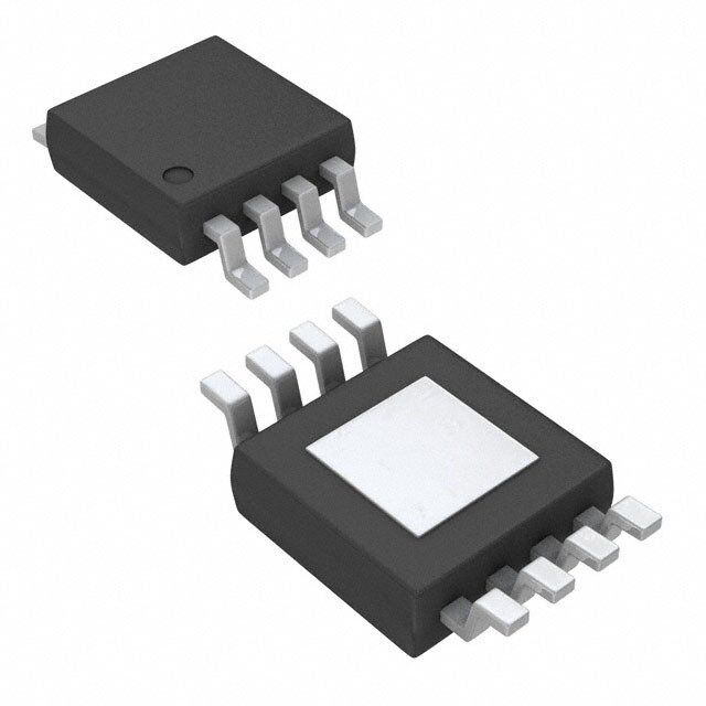
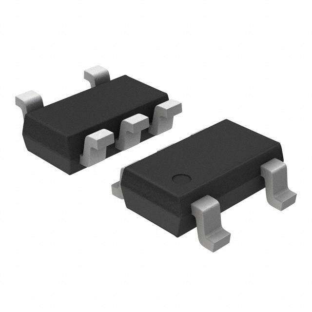
| 供应商器件封装 | 8-MSOP-EP |
| 其它名称 | 576-3879-5 |
| 包装 | 管件 |
| 商标 | Micrel |
| 回动电压—最大值 | 350 mV |
| 安装类型 | 表面贴装 |
| 安装风格 | SMD/SMT |
| 封装 | Tube |
| 封装/外壳 | 8-TSSOP,8-MSOP(0.118",3.00mm 宽)裸焊盘 |
| 封装/箱体 | MSOP-8 |
| 工作温度 | -40°C ~ 125°C |
| 工厂包装数量 | 100 |
| 最大工作温度 | + 125 C |
| 最大输入电压 | 5.5 V |
| 标准包装 | 100 |
| 电压-跌落(典型值) | 0.35V @ 500mA |
| 电压-输入 | 2.5 V ~ 5.5 V |
| 电压-输出 | 2.5V,1.8V |
| 电流-输出 | 500mA |
| 电流-限制(最小值) | 525mA |
| 稳压器拓扑 | 正,固定式 |
| 稳压器数 | 2 |
| 负载调节 | 1 % |
| 输出电压 | 1.8 V, 2.5 V |
| 输出电流 | 500 mA |
| 输出端数量 | 1 Output |
| 输出类型 | Fixed |


- 商务部:美国ITC正式对集成电路等产品启动337调查
- 曝三星4nm工艺存在良率问题 高通将骁龙8 Gen1或转产台积电
- 太阳诱电将投资9.5亿元在常州建新厂生产MLCC 预计2023年完工
- 英特尔发布欧洲新工厂建设计划 深化IDM 2.0 战略
- 台积电先进制程称霸业界 有大客户加持明年业绩稳了
- 达到5530亿美元!SIA预计今年全球半导体销售额将创下新高
- 英特尔拟将自动驾驶子公司Mobileye上市 估值或超500亿美元
- 三星加码芯片和SET,合并消费电子和移动部门,撤换高东真等 CEO
- 三星电子宣布重大人事变动 还合并消费电子和移动部门
- 海关总署:前11个月进口集成电路产品价值2.52万亿元 增长14.8%


PDF Datasheet 数据手册内容提取
MIC5355/6 Dual 500mA µCap Low Dropout, Micropower Linear Regulator General Description Features The MIC5355/6 is an advanced dual, micropower, low 2.5V to 5.5V input voltage range dropout linear regulator. The MIC5355/6 provides low 2% initial output accuracy quiescent current operation, using only 70μA with both Wide output voltage range: 1.0V to 3.3V outputs enabled making it ideal for battery-powered systems. In shutdown, the quiescent current drops to less Low quiescent current: 38µA per output than 1µA. The MIC5355/6 provides two independently- Very low quiescent current in shutdown: <1μA typical controlled high-performance 500mA LDOs with typical µCap stable with 2.2µF ceramic capacitor dropout voltage of 350mV at rated load. In addition, the Low dropout voltage: 350mV at 500mA MIC5355/6 is optimized to provide fast load and line Excellent load/line transient response transient performance with low-ESR ceramic output capacitors, requiring a minimum of only 2.2µF. Independent logic controlled enable pins The MIC5356 also incorporates an active discharge Output discharge circuit: MIC5356 feature when the part is disabled that switches in a 30Ω Current and thermal limit protection load to pull down the output of the regulator. The Power 8-pin ePad MSOP package or 8-pin ePad 3mm MIC5355/6 is available in fixed output voltages in a x 3mm MLF® package thermally-enhanced 8-pin ePad MSOP package or 8-pin ePad 3mm x 3mm MLF® package. Applications Data sheets and support documentation can be found on Micrel’s web site at www.micrel.com. Smart phones GPS, PMP, DSC Notebooks and desktops Digital TV Portable electronics _________________________________________________________________________________________________________________________ Typical Application MLF and MicroLeadFrame are registered trademarks of Amkor Technology, Inc. Micrel Inc. • 2180 Fortune Drive • San Jose, CA 95131 • USA • tel +1 (408) 944-0800 • fax + 1 (408) 474-1000 • http://www.micrel.com March 2012 M9999-031512-A
Micrel, Inc. MIC5355/6 Ordering Information Junction Manufacturer Ordering Marking Part Number(1) Voltage(2) Temperature Package Part Number Code Range MIC5355-SGYMME MIC5355-3.3/1.8YMME 55SG 3.3V/1.8V –40° to +125°C 8-Pin ePad MSOP MIC5355-S4YMME MIC5355-3.3/1.2YMME 55S4 3.3V/1.2V –40° to +125°C 8-Pin ePad MSOP MIC5355-SCYMME MIC5355-3.3/1.0YMME 55SC 3.3V/1.0V –40° to +125°C 8-Pin ePad MSOP MIC5355-G4YMME MIC5355-1.8/1.2YMME 55G4 1.8V/1.2V –40° to +125°C 8-Pin ePad MSOP MIC5355-JGYMME MIC5355-2.5/1.8YMME 55JG 2.5V1.8V –40° to +125°C 8-Pin ePad MSOP MIC5356-SGYMME MIC5356-3.3/1.8YMME 56SG 3.3V/1.8V –40° to +125°C 8-Pin ePad MSOP MIC5356-S4YMME MIC5356-3.3/1.2YMME 56S4 3.3V/1.2V –40° to +125°C 8-Pin ePad MSOP MIC5356-SCYMME MIC5356-3.3/1.0YMME 56SC 3.3V/1.0V –40° to +125°C 8-Pin ePad MSOP MIC5356-G4YMME MIC5356-1.8/1.2YMME 56G4 1.8V/1.2V –40° to +125°C 8-Pin ePad MSOP MIC5356-JGYMME MIC5356-2.5/1.8YMME 56JG 2.5V/1.8V –40° to +125°C 8-Pin ePad MSOP MIC5356-MMYML MI5356-2.8/2.8YML M3M 2.8V/2.8V –40° to +125°C 8-Pin ePad 3mm x 3mm MLF® MIC5356-MGYML MI5356-2.8/1.8YML M3G 2.8V/1.8V –40° to +125°C 8-Pin ePad 3mm x 3mm MLF® Notes: 1. MIC5356 offers Auto-Discharge function. 2. Other voltage available. Contact Micrel for detail. Pin Configuration 8-Pin ePad MSOP (MME) 8-Pin ePad 3mm x 3mm MLF® (ML) Pin Description Pin Number Pin Name Pin Function 1 VIN Supply Input. 2 GND Ground. 3 NC Not internally connected. 4 EN2 Enable Input LDO2. Active High Input. Logic High = On; Logic Low = Off; Do not leave floating. 5 EN1 Enable Input LDO1. Active High Input. Logic High = On; Logic Low = Off; Do not leave floating. 6 NC Not internally connected. 7 VOUT2 LDO2 Output. 8 VOUT1 LDO1 Output. ePad HSPAD Heatsink pad. Connect to ground. March 2012 2 M9999-031512-A
Micrel, Inc. MIC5355/6 Absolute Maximum Ratings(1) Operating Ratings(2) Supply Voltage (V )........................................–0.3V to +6V Supply Voltage (V ).......................................+2.5V to 5.5V IN IN Enable Voltage (V V ).....................–0.3V to V +0.3V Enable Voltage (V V )....................................0V to V EN1, EN2 IN EN1, EN2 IN Power Dissipation (P )...........................Internally Limited(3) Junction Temperature (T )........................–40°C to +125°C D J Lead Temperature (soldering, 10sec.).......................260°C Junction Thermal Resistance Junction Temperature (T )........................–40°C to +125°C 8-Pin ePad MSOP (θ )..................................64.4°C/W J JA Storage Temperature (Ts).........................–65°C to +150°C 8-Pin ePad 3mm x 3mm MLF® (θJA)..................61°C/W ESD Rating(4).................................................ESD Sensitive Electrical Characteristics(5) V = V = V = V +1V; higher of the two outputs; I = I = 100µA; C = C = 2.2 µF; T = +25C, IN EN1 EN2 OUT OUTLDO1 OUTLDO2 OUT1 OUT2 J bold values indicate –40°C to +125°C, unless noted. Parameter Condition Min. Typ. Max. Units Variation from nominal VOUT 2.0 +2.0 Output Voltage Accuracy % Variation from nominal VOUT 3.0 +3.0 Line Regulation V = V + 1V to 5.5V, I = 100µA 0.02 0.3 %/V IN OUT OUT Load Regulation I = 100µA to 500mA 0.3 1 % OUT I = 50mA 40 100 OUT Dropout Voltage mV I = 500mA 350 800 OUT V = High; V = Low; I = 0mA 38 53 EN1 EN2 OUT1 V = Low; V = High; I = 0mA 38 53 EN1 EN2 OUT2 V = V = High; I = I = 0mA 70 100 EN1 EN2 OUT1 OUT2 Ground Pin Current µA V = High; V = Low; I = 500mA 55 90 EN1 EN2 OUT1 V = Low; V = High; I = 500mA 55 90 EN1 EN2 OUT2 V = V = High; I = I = 500mA 105 200 EN1 EN2 OUT1 OUT2 Shutdown Current V = V 0.2V 0.05 1 µA EN1 EN2 Ripple Rejection f = 1kHz; C = 2.2µF; I = 250mA 60 dB OUT OUT Current Limit V = 0V 525 750 1050 mA OUT Output Voltage Noise C = 2.2µF, 10Hz to 100kHz 146 µV OUT RMS Auto-Discharge NFET MIC5356 only; V = V = 0V; V = 3.6V; I = 3mA 30 Ω Resistance EN1 EN2 IN OUT Notes: 1. Exceeding the absolute maximum rating may damage the device. 2. The device is not guaranteed to function outside its operating rating. 3. The maximum allowable power dissipation of any T (ambient temperature) is P = (T T ) / . Exceeding the maximum allowable power A D(MAX) J(MAX) A JA dissipation will result in excessive die temperature and the register will go into thermal shutdown. 4. Devices are ESD sensitive. Handling precautions recommended. Human body model, 1.5kΩ in series with 100pF. 5. Specification for packaged product only. March 2012 3 M9999-031512-A
Micrel, Inc. MIC5355/6 Electrical Characteristics(4) V = V = V = V +1V; higher of the two outputs; I = I = 100µA; C = C = 2.2 µF; T = +25C, IN EN1 EN2 OUT OUTLDO1 OUTLDO2 OUT1 OUT2 J bold values indicate –40°C to +125°C, unless noted. Parameter Condition Min. Typ. Max. Units Enable Inputs (EN1/EN2) Logic Low 0.2 Enable Input Voltage V Logic High 1.2 V 0.2V 0.01 1 IL Enable Input Current µA V 1.2V 0.01 1 IH Turn-On Time 50 125 µs Notes: 1. Exceeding the absolute maximum rating may damage the device. 2. The device is not guaranteed to function outside its operating rating. 3. Devices are ESD sensitive. Handling precautions recommended. Human body model, 1.5kΩ in series with 100pF. 4. Specification for packaged product only. March 2012 4 M9999-031512-A
Micrel, Inc. MIC5355/6 Typical Characteristics Power Supply Rejection Ratio Output Voltage Output Voltage vs. Input Voltage vs. Input Voltage -80 3 2 -70 2.9 -60 250mA E (V)22..78 100μA E (V)1.9 100μA G G dB--5400 500mA OLTA22..56 OLTA1.8 V V --3200 VVEONU T= = V 1IN.8 =V 2.82V 100µA OUTPUT 222...234 500mA OUTPUT 1.7 500mA -10 COUT = 2.2µF 2.1 CIN = COUT = 2.2μF CIN = COUT = 2.2μF 0 2 1.6 10 100 1000 10000 100000 2.5 3 3.5 4 4.5 5 5.5 2.5 3 3.5 4 4.5 5 5.5 FREQUENCY (Hz) INPUT VOLTAGE (V) INPUT VOLTAGE (V) Output Voltage Output Voltage Ground Current vs. vs. Output Current (VOUT1) vs. Output Current (VOUT2) Input Voltage (Single Output) 2.7 2 65 NT 5650 V)2.6 V)1.9 RE 4550 500mA GE ( GE ( CURA)3450 LTA2.5 LTA1.8 ND (μ2350 NO LOAD PUT VO2.4 PUT VO1.7 VIN = VEN2 = 3.5V GROU 1120505 VCVOIENNU 1=T 2 = C= GO 1UN.T8D =V, 2V.E2Nμ2F = VIN OUT2.3 VVIONU =T1 V=E 2N.15 =V 3.5V OUT1.6 VCOINU =T2 C=O 1U.T8 =V 2.2μF 02.5 3 3.5 4 4.5 5 5.5 CIN = COUT = 2.2μF INPUT VOLTAGE (V) 2.2 1.5 0 100 200 300 400 500 0 100 200 300 400 500 OUTPUT CURRENT (mA) OUTPUT CURRENT (mA) Ground Current vs. Input Ground Current Ground Current Voltage (Dual Output) vs. Output Current vs. Temperature (Single Output) 120 120 70 A) 105 A) 105 65 500mA RENT(μ 7950 500mA RENT(μ 7950 DUAL OUTPUT SINGLE OUTPUT T (μA)556050 GROUND CUR 134650500 VCVOIENNU 1=T 1 = C= VO 2UE.NT5 2=V = ,2 V.V2OIμNUFT2 = 1.8V NO LOAD GROUND CUR 134650500 VCIINN == 3C.O5UVT = 2.2μF ROUND CURREN12233445050505 NO LOAD VVOENU1T 1= =V2I.N5 =V 3V 2.5 3 3.5 4 4.5 5 5.5 0 50 100150200250300350400450500 G10 VEN2 = GND INPUT VOLTAGE (V) OUTPUT CURRENT (mA) 5 CIN = COUT = 2.2μF 0 -40 -20 0 20 40 60 80 100 120 TEMPERATURE (°C) March 2012 5 M9999-031512-A
Micrel, Inc. MIC5355/6 Typical Characteristics (Continued) Dropout Voltage Ground Current Dropout Voltage vs. Output Current vs. Temperature (Dual Output) vs. Temperature 120 450 350 GROUND CURRENT (μA) 102468000000 NO LOAD VVCOEINNU 1=T 1= C= VO 2UE.NT5 2=V = ,2 V.V2OIμN5UF 0T=20 3=m. 5A1V.8V DROPOUT VOLTAGE (mV) 11223340505050500000000 CIN = COUT = 2.23μ0F0mA 1505m0mAA500mA DROPOUT VOLTAGE (mV) 11223050505000000 VOUT1 = 2.5V -40 -20 0 20 40 60 80 100 120 0 CIN = COUT = 2.2μF -40 -20 0 20 40 60 80 100 120 0 TEMPERATURE (°C) TEMPERATURE (°C) 0 100 200 300 400 500 OUTPUT CURRENT (mA) Current Limit vs. Input Voltage Output Noise Spectral Density 900 1 A)850 VOUT1 = 2.5V m T (800 Hz)0.1 NT LIMI750 E (µV/√ RRE700 VOUT2 = 1.8V NOIS0.01 V VINO U=T 23 =.5 V1.81V CU CIN - COUT = 2.2µF 650 Noise (10Hz to 100Khz) =146µVrms CIN = COUT = 2.2μF 0.001 600 10 100 1000 10000 100000 1000000 2.5 3 3.5 4 4.5 5 5.5 FREQUENCY (Hz) INPUT VOLTAGE (V) March 2012 6 M9999-031512-A
Micrel, Inc. MIC5355/6 Functional Characteristics March 2012 7 M9999-031512-A
Micrel, Inc. MIC5355/6 Functional Diagrams MIC5355 Block Diagram MIC5356 Block Diagram March 2012 8 M9999-031512-A
Micrel, Inc. MIC5355/6 Application Information Enable/Shutdown MIC5355/6 is a dual 500mA LDO. The MIC5356 The MIC5355/6 comes with two active high enable pins includes an auto-discharge circuit for each LDO output that allow each regulator to be disabled independently. that is activated when the output is disabled. The Forcing the enable pin low disables the regulator and MIC5355/6 regulator is fully protected from damage due places it into an off mode current state drawing virtually to fault conditions through linear current limiting and zero current. When disabled, the MIC5356 switches an thermal shutdown. internal 30Ω load on the regulator output to discharge the external capacitor. Input Capacitor Forcing the enable pin high enables the output voltage. The MIC5355/6 is a high-performance, high-bandwidth The active high enable pin uses CMOS technology and device. A 2.2µF input capacitor from the input pin to cannot be left floating. A floating enable pin may cause ground is required to provide stability. Low-ESR ceramic an indeterminate state on the output. capacitors provide optimal performance in small board area. Additional high-frequency capacitors, such as Thermal Considerations small valued NPO dielectric type capacitors, help filter The MIC5355/6 is designed to provide two 500mA out high-frequency noise and are good practice in any continuous current outputs in a small package. RF based circuit. X5R or X7R dielectrics are Maximum operating temperature can be calculated recommended for the input capacitor. Y5V dielectrics based on the output currents and the voltage drop lose most of their capacitance over temperature and are across the part. For example, if the input voltage is 3.0V, therefore not recommended. V = 2.5V, V = 1.8V and each with an output OUT1 OUT2 current = 500mA. The actual power dissipation of the Output Capacitor regulator circuit can be determined using the equation: The MIC5355/6 requires an output capacitor of 2.2µF or greater to maintain stability. The design is optimized for use with low-ESR ceramic chip capacitors. High-ESR PD = (VIN VOUT1) IOUT (VIN VOUT2) IOUT2 VIN IGND capacitors may cause high-frequency oscillation. The output capacitor can be increased, but performance has Because this is CMOS device and the ground current is been optimized for a 2.2µF ceramic output capacitor and typically <100µA over the load range, the power does not improve significantly with larger capacitance. dissipation contributed by the ground current is <1% X7R and X5R dielectric ceramic capacitors are which can be ignored for this calculation: recommended because of their temperature performance. X7R capacitors change capacitance by P = (3.0V – 2.5V) × 500mA + (3.0V – 1.8V) × 500mA 15% over their operating temperature range and are the D most stable type of ceramic capacitors. Z5U and Y5V P = 0.85W D dielectric capacitors change value by as much as 50% and 60% respectively over their operating temperature To determine the maximum ambient operating ranges. To use a ceramic chip capacitor with Y5V temperature of the package, use the junction to ambient dielectric the value must be much higher than an X7R thermal resistance of the device and the following basic ceramic capacitor to ensure the same minimum equation: capacitance over the equivalent operating temperature range. T T No Load Stability P J(MAX) A D(MAX) θ Unlike many other voltage regulators, the MIC5355/6 will JA remain stable and in regulation with no load. T = 125°C J(MAX) θ = 64.4°C/W JA March 2012 9 M9999-031512-A
Micrel, Inc. MIC5355/6 Substituting P for P and solving for the ambient D D(MAX) operating temperature will give the maximum operating conditions for the regulator circuit. The junction to ambient thermal resistance for the minimum footprint is 64.4°C/W. The maximum power dissipation must not be exceeded for proper operation. For example, when operating a 2.5V/1.8V application with an input voltage of 3.0V and 500mA at each output with a minimum footprint layout, the maximum ambient operating temperature T can be determined A as follows: 0.85W = (125°C – T )/(64.4°C/W) A T = 70.3°C A Therefore, a MIC5355-JGYMME application with 500mA at each output current can accept an ambient operating temperature of 70.3°C in a small 8-pin ePad MSOP package. For a full discussion of heat sinking and thermal effects on voltage regulators refer to the “Regulator Thermals” section of Micrel’s Designing with Low-Dropout Voltage Regulators handbook. This information can be found on Micrel's website at: http://www.micrel.com/_PDF/other/LDOBk_ds.pdf March 2012 10 M9999-031512-A
Micrel, Inc. MIC5355/6 Typical Application Schematic Bill of Materials Item Part Number Manufacturer Description Qty. C1, C2, C3 C1005X5R0J225M TDK(1) 2.2µF ceramic capacitor, 6.3V, X5R, size 0402 3 U1 MIC5355/6-xxYMME Micrel, Inc.(2) Dual 500mA µCap Low-Dropout, Micropower Linear Regulator 1 Notes: 1. TDK: www.tdk.com. 2. Micrel, Inc.: www.micrel.com. March 2012 11 M9999-031512-A
Micrel, Inc. MIC5355/6 Typical Application Schematic (Continued) Bill of Materials Item Part Number Manufacturer Description Qty. C1, C2, C3 C1005X5R0J225M TDK(1) 2.2µF ceramic capacitor, 6.3V, X5R, size 0402 3 U1 MIC5355/6-xxYML Micrel, Inc.(2) Dual 500mA µCap Low-Dropout, Micropower Linear Regulator 1 Notes: 3. TDK: www.tdk.com. 4. Micrel, Inc.: www.micrel.com. March 2012 12 M9999-031512-A
Micrel, Inc. MIC5355/6 PCB Layout Recommendations (MME Package) Top Layer Bottom Layer March 2012 13 M9999-031512-A
Micrel, Inc. MIC5355/6 PCB Layout Recommendations (ML Package) Top Layer Bottom Layer March 2012 14 M9999-031512-A
Micrel, Inc. MIC5355/6 Package Information 8-Pin ePad MSOP (MME) 8-Pin ePad 3mm x 3mm MLF® (ML) March 2012 15 M9999-031512-A
Micrel, Inc. MIC5355/6 Package Information (Continued) Red circle indicates Thermal Via. Size should be .300 −.350mm in diameter, 1/00mm pitch, and it should be connected to GND plane for maximum thermal performance. 8-Pin ePad MSOP (MME) March 2012 16 M9999-031512-A
Micrel, Inc. MIC5355/6 Package Information (Continued) Red circle indicates Thermal Via. Size should be .300 −.350mm in diameter, 1/00mm pitch, and it should be connected to GND plane for maximum thermal performance. 8-Pin ePad 3mm x 3mm MLF® (ML) March 2012 17 M9999-031512-A
Micrel, Inc. MIC5355/6 MICREL, INC. 2180 FORTUNE DRIVE SAN JOSE, CA 95131 USA TEL +1 (408) 944-0800 FAX +1 (408) 474-1000 WEB http://www.micrel.com Micrel makes no representations or warranties with respect to the accuracy or completeness of the information furnished in this data sheet. This information is not intended as a warranty and Micrel does not assume responsibility for its use. Micrel reserves the right to change circuitry, specifications and descriptions at any time without notice. No license, whether express, implied, arising by estoppel or otherwise, to any intellectual property rights is granted by this document. Except as provided in Micrel’s terms and conditions of sale for such products, Micrel assumes no liability whatsoever, and Micrel disclaims any express or implied warranty relating to the sale and/or use of Micrel products including liability or warranties relating to fitness for a particular purpose, merchantability, or infringement of any patent, copyright or other intellectual property right. Micrel Products are not designed or authorized for use as components in life support appliances, devices or systems where malfunction of a product can reasonably be expected to result in personal injury. Life support devices or systems are devices or systems that (a) are intended for surgical implant into the body or (b) support or sustain life, and whose failure to perform can be reasonably expected to result in a significant injury to the user. A Purchaser’s use or sale of Micrel Products for use in life support appliances, devices or systems is a Purchaser’s own risk and Purchaser agrees to fully indemnify Micrel for any damages resulting from such use or sale. © 2012 Micrel, Incorporated. March 2012 18 M9999-031512-A