ICGOO在线商城 > 传感器,变送器 > 温度传感器 - 温控器 - 固态 > LM26CIM5-SPA/NOPB

 Datasheet下载
- 型号: LM26CIM5-SPA/NOPB
- 制造商: Texas Instruments
- 库位|库存: xxxx|xxxx
- 要求:
| 数量阶梯 | 香港交货 | 国内含税 |
| +xxxx | $xxxx | ¥xxxx |
查看当月历史价格
查看今年历史价格
LM26CIM5-SPA/NOPB产品简介:
ICGOO电子元器件商城为您提供LM26CIM5-SPA/NOPB由Texas Instruments设计生产,在icgoo商城现货销售,并且可以通过原厂、代理商等渠道进行代购。 LM26CIM5-SPA/NOPB价格参考¥4.03-¥10.01。Texas InstrumentsLM26CIM5-SPA/NOPB封装/规格:温度传感器 - 温控器 - 固态, Thermostat 75°C Active Low Open Drain SOT-23-5。您可以下载LM26CIM5-SPA/NOPB参考资料、Datasheet数据手册功能说明书,资料中有LM26CIM5-SPA/NOPB 详细功能的应用电路图电压和使用方法及教程。
Texas Instruments(德州仪器)的LM26CIM5-SPA/NOPB 是一款温度传感器,属于温控器 - 固态类别。它具有多种应用场景,特别是在需要精确温度监控和控制的系统中表现优异。

 主要应用场景:

1. 工业自动化与控制系统:
   LM26CIM5-SPA/NOPB 可用于工业自动化设备中的温度监测与控制。例如,在制造过程中,许多机器和设备需要在特定温度范围内运行以确保产品质量。该传感器可以实时监控这些设备的温度,并通过反馈机制调整温度,确保生产过程的稳定性和安全性。

2. 消费电子产品:
   在家用电器如空调、冰箱、微波炉等中,温度控制是关键功能之一。LM26CIM5-SPA/NOPB 能够提供高精度的温度测量,帮助设备维持最佳工作温度,提高能效并延长使用寿命。

3. 医疗设备:
   医疗设备如恒温箱、孵化器等对温度有严格要求。LM26CIM5-SPA/NOPB 可以确保这些设备在设定的温度范围内稳定运行,保障医疗实验和治疗的安全性与准确性。

4. 通信设备:
   通信基站、服务器和其他网络设备通常需要保持在一个稳定的温度范围内以防止过热或低温损坏。该传感器可以集成到这些设备中,实现自动化的温度监控和调节,确保设备的正常运行。

5. 汽车电子:
   在汽车电子系统中,发动机、电池管理系统等部件需要精确的温度监控。LM26CIM5-SPA/NOPB 可以用于检测这些关键部件的温度,防止因过热或过冷导致的故障,提升车辆的安全性和可靠性。

 特点和优势:

- 高精度:提供准确的温度测量,适用于对温度敏感的应用。
- 低功耗:适合电池供电的便携式设备,延长续航时间。
- 宽温度范围:支持广泛的温度区间,适应不同环境需求。
- 小型封装:节省空间,便于集成到紧凑型设计中。

综上所述,LM26CIM5-SPA/NOPB 在多个领域中都有广泛的应用,凭借其高精度、低功耗和可靠性能,成为温度监控和控制的理想选择。
| 参数 | 数值 |
| 产品目录 | |
| 描述 | IC THERMOSTAT DGTL LOPWR SOT23-5恒温器 Accurate Factory Preset Thermostat |
| 产品分类 | 温度传感器,变送器温度传感器 |
| 品牌 | Texas Instruments |
| 产品手册 | |
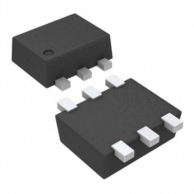
| 产品图片 |
|
| rohs | 符合RoHS无铅 / 符合限制有害物质指令(RoHS)规范要求 |
| 产品系列 | 恒温器,Texas Instruments LM26CIM5-SPA/NOPBPowerWise® |
| 数据手册 | |
| 产品型号 | LM26CIM5-SPA/NOPB |
| 产品 | Digital Thermostats |
| 产品目录页面 | |
| 产品种类 | 恒温器 |
| 供应商器件封装 | SOT-23-5 |
| 其它名称 | *LM26CIM5-SPA/NOPB |
| 准确性 | +/- 3 C |
| 制造商产品页 | http://www.ti.com/general/docs/suppproductinfo.tsp?distId=10&orderablePartNumber=LM26CIM5-SPA/NOPB |
| 功能 | Over Temp Shutdown |
| 包装 | 剪切带 (CT) |
| 商标 | Texas Instruments |
| 安装类型 | 表面贴装 |
| 封装 | Reel |
| 封装/外壳 | SC-74A,SOT-753 |
| 工厂包装数量 | 1000 |
| 开关温度 | 75°C |
| 开路温度 | + 75 C |
| 感应温度 | 75°C 跳变点 |
| 标准包装 | 1 |
| 温度范围 | - 55 C to + 110 C |
| 特性 | - |
| 电压-电源 | 2.7 V ~ 5.5 V |
| 电压额定值 | 2.7 V to 5.5 V |
| 电流-电源 | 16µA |
| 电流-输出(最大值) | - |
| 电流额定值 | 20 uA |
| 精度 | ±3°C |
| 系列 | LM26 |
| 输出 | 低有效 |
| 输出类型 | 低态有效/开漏极,电压 |


- 商务部:美国ITC正式对集成电路等产品启动337调查
- 曝三星4nm工艺存在良率问题 高通将骁龙8 Gen1或转产台积电
- 太阳诱电将投资9.5亿元在常州建新厂生产MLCC 预计2023年完工
- 英特尔发布欧洲新工厂建设计划 深化IDM 2.0 战略
- 台积电先进制程称霸业界 有大客户加持明年业绩稳了
- 达到5530亿美元!SIA预计今年全球半导体销售额将创下新高
- 英特尔拟将自动驾驶子公司Mobileye上市 估值或超500亿美元
- 三星加码芯片和SET,合并消费电子和移动部门,撤换高东真等 CEO
- 三星电子宣布重大人事变动 还合并消费电子和移动部门
- 海关总署:前11个月进口集成电路产品价值2.52万亿元 增长14.8%


PDF Datasheet 数据手册内容提取
Product Sample & Technical Tools & Support & Folder Buy Documents Software Community LM26 SNIS115S–MAY2001–REVISEDSEPTEMBER2015 LM26 SOT-23, ±3°C Accurate, Factory-Preset Thermostat 1 Features 3 Description • InternalComparatorWithPinProgrammable2°C The LM26 is a precision, single digital-output, low- 1 power thermostat comprised of an internal reference, or10°CHysteresis DAC, temperature sensor and comparator. Utilizing • NoExternalComponentsRequired factory programming, it can be manufactured with • Open-DrainorPush-PullDigitalOutput;Supports different trip points as well as different digital output CMOSLogicLevels functionality. The trip point (T ) can be preset at the OS factory to any temperature in the range of −55°C to • InternalTemperatureSensorWithV Output TEMP 110°C in 1°C increments. The LM26 has one digital Pin output (OS/OS/US/US), one digital input (HYST) and • V OutputAllowsAfter-AssemblySystem TEMP one analog output (V ). The digital output stage TEMP Testing can be preset as either open-drain or push-pull. In • InternalVoltageReferenceandDACforTrip-Point addition, it can be factory programmed to be active Setting HIGH or LOW. The digital output can be factory programmed to indicate an over temperature • CurrentlyAvailablein5-pinSOT-23Plastic shutdown event (OS or OS) or an under temperature Package shutdown event (US or US). When preset as an • ExcellentPowerSupplyNoiseRejection overtemperature shutdown (OS) it will go LOW to • ULRecognizedComponent indicate that the die temperature is over the internally preset T and go HIGH when the temperature goes • KeySpecifications OS below (T –T ). Similarly, when preprogrammed OS HYST – PowerSupplyVoltage2.7Vto5.5V as an undertemperature shutdown (US) it will go – PowerSupplyCurrent HIGH to indicate that the temperature is below T US 40μA(Maximum)16 μA(Typical) and go LOW when the temperature is above (T +T ). The typical hysteresis, T , can be set – HysteresisTemperature2°Cor10°C(Typical) US HYST HYST to 2°C or 10°C and is controlled by the state of the HYST pin. A V analog output provides a voltage 2 Applications TEMP that is proportional to temperature and has a −10.82 • MicroprocessorThermalManagement mV/°Coutputslope. • Appliances AvailablepartsaredetailedintheDeviceComparison • PortableBatteryPoweredSystems Table. For other part options, contact a Texas Instruments Distributor or Sales Representative for • FanControl information on minimum order qualification. The • IndustrialProcessControl LM26 is currently available in a 5-lead SOT-23 • HVACSystems package. • RemoteTemperatureSensing DeviceInformation(1) • ElectronicSystemProtection PARTNUMBER PACKAGE BODYSIZE(NOM) LM26 SOT-23(5) 2.90mm×1.60mm (1) For all available packages, see the orderable addendum at theendofthedatasheet. LM26CIM5-TPASimplifiedBlockDiagramandConnectionDiagram TOS HYST HYST OS TOS - THYST REF Temp. of GND + Leads TEMP - SENSOR OS VTEMP LM26TPA Vto+ 5 =.5 2V.7V HYST=GND for 10°C Hysteresis HYST = V+ for 2°C Hysteresis VTEMP = (-3.479 x 10⁻⁶ x (T-30)2) + (-1.082 x 10⁻² x (T-30)) + 1.8015V TheLM26CIM5-TPAhasafixedtrippointof85°C.Forothertrippointandoutputfunctionavailability,pleaseseethe DeviceComparisonTableorcontactTexasInstruments. 1 An IMPORTANT NOTICE at the end of this data sheet addresses availability, warranty, changes, use in safety-critical applications, intellectualpropertymattersandotherimportantdisclaimers.PRODUCTIONDATA.
LM26 SNIS115S–MAY2001–REVISEDSEPTEMBER2015 www.ti.com Table of Contents 1 Features.................................................................. 1 8.4 DeviceFunctionalModes..........................................9 2 Applications........................................................... 1 9 ApplicationandImplementation........................ 10 3 Description............................................................. 1 9.1 ApplicationInformation............................................10 4 RevisionHistory..................................................... 2 9.2 TypicalApplication..................................................10 9.3 SystemExamples...................................................11 5 DeviceComparisonTable..................................... 3 10 PowerSupplyRecommendations..................... 12 6 PinConfigurationandFunctions......................... 4 11 Layout................................................................... 12 7 Specifications......................................................... 4 11.1 LayoutGuidelines.................................................12 7.1 AbsoluteMaximumRatings......................................4 11.2 LayoutExample....................................................12 7.2 ESDRatings..............................................................5 11.3 ThermalConsiderations........................................13 7.3 RecommendedOperatingConditions.......................5 11.4 PartNumberTemplate..........................................14 7.4 ThermalInformation..................................................5 12 DeviceandDocumentationSupport................. 15 7.5 ElectricalCharacteristics..........................................5 7.6 TypicalCharacteristics..............................................6 12.1 CommunityResources..........................................15 12.2 Trademarks...........................................................15 8 DetailedDescription.............................................. 7 12.3 ElectrostaticDischargeCaution............................15 8.1 Overview...................................................................7 12.4 Glossary................................................................15 8.2 FunctionalBlockDiagrams.......................................7 13 Mechanical,Packaging,andOrderable 8.3 FeatureDescription...................................................8 Information........................................................... 15 4 Revision History NOTE:Pagenumbersforpreviousrevisionsmaydifferfrompagenumbersinthecurrentversion. ChangesfromRevisionR(February2013)toRevisionS Page • AddedPinConfigurationandFunctionssection,HandlingRatingtable,FeatureDescriptionsection,Device FunctionalModes,ApplicationandImplementationsection,PowerSupplyRecommendationssection,Layout section,DeviceandDocumentationSupportsection,andMechanical,Packaging,andOrderableInformation section ................................................................................................................................................................................... 1 • RemovedPartNumberTemplatetable ................................................................................................................................. 6 • RemovedTemperatureTripPointAccuracytable ................................................................................................................ 6 ChangesfromRevisionQ(September2011)toRevisionR Page • ChangedlayoutofNationalDataSheettoTIformat........................................................................................................... 11 2 SubmitDocumentationFeedback Copyright©2001–2015,TexasInstrumentsIncorporated ProductFolderLinks:LM26
LM26 www.ti.com SNIS115S–MAY2001–REVISEDSEPTEMBER2015 5 Device Comparison Table OrderNumber TopMark TripPoint OutputFunction Setting BulkRail(1000Units) Tape&Reel(3000Units) LM26CIM5-BPB LM26CIM5X-BPB TBPB -45°C Active-Low,Open-Drain,USoutput LM26CIM5-DPB LM26CIM5X-DPB TDPB -25°C Active-Low,Open-Drain,USoutput LM26CIM5-HHD LM26CIM5X-HHD THHD 0°C Active-High,Push-Pull,USoutput LM26CIM5-NPA LM26CIM5X-NPA TNPA 45°C Active-Low,Open-Drain,OSoutput LM26CIM5-RPA LM26CIM5X-RPA TRPA 65°C Active-Low,Open-Drain,OSoutput LM26CIM5-SHA LM26CIM5X-SHA TSHA 75°C Active-Low,Open-Drain,OSoutput LM26CIM5-SPA LM26CIM5X-SPA TSPA 70°C Active-Low,Open-Drain,OSoutput LM26CIM5-TPA LM26CIM5X-TPA TTPA 85°C Active-Low,Open-Drain,OSoutput LM26CIM5-VHA LM26CIM5X-VHA TVHA 90°C Active-Low,Open-Drain,OSoutput LM26CIM5-VPA LM26CIM5X-VPA TVPA 95°C Active-Low,Open-Drain,OSoutput LM26CIM5-XHA LM26CIM5X-XHA TXHA 100°C Active-Low,Open-Drain,OSoutput LM26CIM5-XPA LM26CIM5X-XPA TXPA 105°C Active-Low,Open-Drain,OSoutput LM26CIM5-YHA LM26CIM5X-YHA TYHA 110°C Active-Low,Open-Drain,OSoutput LM26CIM5-YPA LM26CIM5X-YPA TYPA 115°C Active-Low,Open-Drain,OSoutput LM26CIM5-ZHA LM26CIM5X-ZHA TZHA 120°C Active-Low,Open-Drain,OSoutput Copyright©2001–2015,TexasInstrumentsIncorporated SubmitDocumentationFeedback 3 ProductFolderLinks:LM26
LM26 SNIS115S–MAY2001–REVISEDSEPTEMBER2015 www.ti.com 6 Pin Configuration and Functions DBVPackage 5-PinSOT-23 (TopView) PinFunctions PIN TYPE DESCRIPTION NO. NAME 1 HYST Input Hysteresiscontrol,digitalinput;connecttoGNDfor10°CorV+for2°C Power Ground,connectedtothebacksideofthediethroughleadframe;connectto 2 GND systemground Output Analogoutputvoltageproportionaltotemperature;leavefloatingorconnecttoa 3 V TEMP highimpedancenode. 4 V+ Power Supplyinput;connectto2.7Vto5.5Vwitha0.1-μFbypasscapacitor. Output OvertemperatureShutdownopen-drainactivelowthermostatdigitaloutput; OS connecttocontrollerinterrupt,system/powersupplyshutdown;pullupresistor≥10 kΩ OS Output OvertemperatureShutdownpush-pullactivehighthermostatdigitaloutput; connecttocontrollerinterrupt,system/powersupplyshutdown 5(1) US Output UndertemperatureShutdownopen-drainactivelowthermostatdigitaloutput; connecttocontrollerinterrupt,system/powersupplyshutdown;pullupresistor≥10 kΩ US Output UndertemperatureShutdownpush-pullactivehighthermostatdigitaloutput; connecttocontrollerinterrupt,system/powersupplyshutdown (1) Pin5functionalityandtrippointsettingareprogrammedduringLM26manufacture. 7 Specifications 7.1 Absolute Maximum Ratings overoperatingfree-airtemperaturerange(unlessotherwisenoted) (1) MIN MAX UNIT InputVoltage 6 V InputCurrentatanypin (2) 5 mA PackageInputCurrent (2) 20 mA PackageDissipationatT =25°C(3) 500 mW A Soldering VaporPhase(60seconds) 215 Information(4) SOT-23Package Infrared(15seconds) 220 °C StorageTemperature,T −65 150 °C stg (1) StressesbeyondthoselistedunderAbsoluteMaximumRatingsmaycausepermanentdamagetothedevice.Thesearestressratings only,whichdonotimplyfunctionaloperationofthedeviceattheseoranyotherconditionsbeyondthoseindicatedunderRecommended OperatingConditions.Exposuretoabsolute-maximum-ratedconditionsforextendedperiodsmayaffectdevicereliability. (2) Whentheinputvoltage(V)atanypinexceedsthepowersupply(V <GNDorV >V+),thecurrentatthatpinshouldbelimitedto5mA. I I I The20-mAmaximumpackageinputcurrentratinglimitsthenumberofpinsthatcansafelyexceedthepowersupplieswithaninput currentof5mAtofour.Undernormaloperatingconditionsthemaximumcurrentthatpins2,4or5canhandleislimitedto5mAeach. (3) ThemaximumpowerdissipationmustbederatedatelevatedtemperaturesandisdictatedbyT (maximumjunctiontemperature), JMAX θ (junctiontoambientthermalresistance)andT (ambienttemperature).Themaximumallowablepowerdissipationatany JA A temperatureisP =(T –T )/θ orthenumbergivenintheAbsoluteMaximumRatings,whicheverislower.Forthisdevice,T D JMAX A JA JMAX =150°C.Forthisdevicethetypicalthermalresistance(θ )ofthedifferentpackagetypeswhenboardmountedfollow: JA (4) SeetheURLhttp://www.ti.com/packagingforotherrecommendationsandmethodsofsolderingsurfacemountdevices. 4 SubmitDocumentationFeedback Copyright©2001–2015,TexasInstrumentsIncorporated ProductFolderLinks:LM26
LM26 www.ti.com SNIS115S–MAY2001–REVISEDSEPTEMBER2015 7.2 ESD Ratings VALUE UNIT Humanbodymodel(HBM) ±2500 V Electrostaticdischarge(1) V (ESD) MachineModel ±250 (1) Thehumanbodymodelisa100-pFcapacitordischargethrougha1.5-kΩresistorintoeachpin.Themachinemodelisa200-pF capacitordischargeddirectlyintoeachpin. 7.3 Recommended Operating Conditions overoperatingfree-airtemperaturerange(unlessotherwisenoted)(1) MIN MAX UNIT SpecifiedTemperatureRange(T ≤T ≤T ) −55 125 °C MIN A MAX PositiveSupplyVoltage(V+) 2.7 5.5 V MaximumV 5.5 V OUT (1) AbsoluteMaximumRatingsindicatelimitsbeyondwhichdamagetothedevicemayoccur.OperatingRatingsindicateconditionsfor whichthedeviceisfunctional,butdonotguaranteespecificperformancelimits.Forguaranteedspecificationsandtestconditions,see theElectricalCharacteristics.Theguaranteedspecificationsapplyonlyforthetestconditionslisted.Someperformancecharacteristics maydegradewhenthedeviceisnotoperatedunderthelistedtestconditions. 7.4 Thermal Information LM26 THERMALMETRIC(1) DBV(SOT-23) UNIT 5PINS R Junction-to-ambientthermalresistance 250 °C/W θJA (1) Formoreinformationabouttraditionalandnewthermalmetrics,seetheSemiconductorandICPackageThermalMetricsapplication report,SPRA953. 7.5 Electrical Characteristics ThefollowingspecificationsapplyforV+=2.7V to5.5V ,andV loadcurrent=0µAunlessotherwisespecified.All DC DC TEMP limitsapplyforT =T =T toT unlessotherwisespecified. A J MIN MAX PARAMETER TESTCONDITIONS MIN(1) TYP(2) MAX(1) UNIT TEMPERATURESENSOR TripPointAccuracy(IncludesV ,DAC, –55°C≤T ≤+110°C ±3 °C REF A ComparatorOffset,andTemperature Sensitivityerrors) TA=+120°C ±4 °C HYST=GND 11 °C TripPointHysteresis HYST=V+ 2 °C V OutputTemperatureSensitivity −10.82 mV/°C TEMP V TemperatureSensitivityErrorto −30°C≤T ≤120°C ±3 °C TEMP A Equation: VO=(−3.479×10⁻⁶×(T−30)2)+ −12505°°CC,≤TA≤ 4.5V≤V+≤5.5V ±3 °C (−1.082×10⁻²×(T−30))+1.8015V T =30°C ±2.5 °C A Source≤1μA 0.070 mV V LoadRegulation TEMP Sink≤40μA 0.7 mV +2.7V≤V+≤+5.5V, V LineRegulation −0.2 mV/V TEMP −30°C≤T ≤+120°C A T =25°C 16 20 µA A I SupplyCurrent S 40 (1) LimitsareguaranteedtoTI'sAOQL(AverageOutgoingQualityLevel). (2) TypicalsareatT =T =25°Candrepresentmostlikelyparametricnorm. J A Copyright©2001–2015,TexasInstrumentsIncorporated SubmitDocumentationFeedback 5 ProductFolderLinks:LM26
LM26 SNIS115S–MAY2001–REVISEDSEPTEMBER2015 www.ti.com Electrical Characteristics (continued) ThefollowingspecificationsapplyforV+=2.7V to5.5V ,andV loadcurrent=0µAunlessotherwisespecified.All DC DC TEMP limitsapplyforT =T =T toT unlessotherwisespecified. A J MIN MAX PARAMETER TESTCONDITIONS MIN(1) TYP(2) MAX(1) UNIT DIGITALOUTPUTANDINPUT I Logical1OutputLeakageCurrent (3) T =25°C V+=+5.0V 0.001 1 µA OUT(1) A I =+1.2mAandV+≥2.7V; VOUT(0) Logical0OutputVoltage IOUT=+3.2mAandV+≥4.5V(4) 0.4 V OUT I =500µA,V+≥2.7V 0.8×V+ V SOURCE V Logical1Push-PullOutputVoltage OUT(1) I =800µA,V+≥4.5V V+−1.5 V SOURCE V HYSTInputLogical1ThresholdVoltage 0.8×V+ V IH V HYSTInputLogical0ThresholdVoltage 0.2×V+ V IL (3) The1-µAlimitisbasedonatestinglimitationanddoesnotreflecttheactualperformanceofthepart.Expecttoseeadoublingofthe currentforevery15°Cincreaseintemperature.Forexample,the1-nAtypicalcurrentat25°Cwouldincreaseto16nAat85°C. (4) Takecaretoincludetheeffectsofselfheatingwhensettingthemaximumoutputloadcurrent.ThepowerdissipationoftheLM26would increaseby1.28mWwhenI =3.2mAandV =0.4V.Withathermalresistanceof250°C/W,thispowerdissipationwouldcause OUT OUT anincreaseinthedietemperatureofabout0.32°Cduetoselfheating.Selfheatingisnotincludedinthetrippointaccuracy specification. 7.6 Typical Characteristics 100 80 A) µ ( nt 60 e urr C y 40 pl p u S 20 0 ±60 ±40 ±20 0 20 40 60 80 100 120 140 Temperature(°C) C001 Figure1.PowerSupplyCurrentTemperatureDependence 6 SubmitDocumentationFeedback Copyright©2001–2015,TexasInstrumentsIncorporated ProductFolderLinks:LM26
LM26 www.ti.com SNIS115S–MAY2001–REVISEDSEPTEMBER2015 8 Detailed Description 8.1 Overview The LM26 is a factory preset thermostat (temperature switch) that includes an integrated temperature sensor, reference voltage, DAC and comparator. The LM26 can be factory programmed to have a trip point anywhere in the range of −55°C to +120°C. The output functionality can also be changed during the manufacturing process, asdescribedinthefunctionalblockdiagrams.Availableoptionsinclude: • OS:activelow,opendrainthatindicatesanovertemperatureshutdownevent(mostcommon) • US:activelow,open-drainthatindicatesanundertemperatureshutdownevent • OS:activehigh,push-pullthatindicatesanovertemperatureshutdownevent • US:activehigh,push-pullthatindicatesanundertemperatureshutdownevent The internal temperature sensor is brought out on the V pin and can be used to determine the temperature TEMP that the LM26 is reading by monitoring with an ADC. It has a negative temperature coefficient (NTC) of approximately -10mV/°C. This pin also allows after assembly PCB testing (see section After Assembly PCB Testingformoredetails). The comparator hysteresis is selectable by the state of the HYST. Two values are available 10°C or 2°C. Comparator hysteresis is essential, as it prevents comparator output chattering when the temperature is at the comparator threshold set point (REF as shown in the functional block diagrams). Once the comparator trips the hysteresis function changes the comparator threshold (REF) level such that the output remains locked in the activestate.Thethresholdischangedbyeither10°Cor2°CasprogrammedbythestateoftheHYSTpin. 8.2 Functional Block Diagrams HYST OS HYST REF GND + TEMP - SENSOR + VTEMP V LM26__A Figure2. LM26-__AOutputPinBlockDiagram HYST US HYST REF GND - TEMP + SENSOR + VTEMP V LM26__B Figure3. LM26-__BOutputPinBlockDiagram HYST OS HYST V+ REF - GND TEMP + SENSOR + VTEMP V LM26__C Figure4. LM26-__COutputPinBlockDiagram Copyright©2001–2015,TexasInstrumentsIncorporated SubmitDocumentationFeedback 7 ProductFolderLinks:LM26
LM26 SNIS115S–MAY2001–REVISEDSEPTEMBER2015 www.ti.com Functional Block Diagrams (continued) HYST US HYST V+ REF - GND TEMP + SENSOR + VTEMP V LM26__D Figure5. LM26-__DOutputPinBlockDiagram 8.3 Feature Description 8.3.1 Hysteresis The HYST pin level sets the comparator hysteresis. Setting the HYST pin to GND selects 10°C hysteresis, while setting it to V+ selects 2°C. A series resistor can be used for protection purposes. The input leakage current of thepinislessthan10µA.ThevalueoftheresistorwilldependonthevalueofV+aswellastheleakagecurrent. For example with V+ = 3.3 V the input threshold level for V = 0.8 × 3.3 V = 2.64 V, thus the voltage drop across IH the resistor should be less than 0.66 V. The 10-µA input leakage current requires the resistor value to be less than66kΩ. 8.3.2 V Output TEMP TheV outputprovidesanoutputvoltagethatcanbeusedtodeterminethetemperaturereadingoftheLM26. TEMP ThetemperaturereadingoftheLM26canbecalculatedusingtheequation: V = (-3.47´10-6´(T-30)2) + (1.082´10-2´(T-30)) + 1.8015 V O (1) or 1.8015-V T =-1525.04+ 2.4182´106 + TEMP 3.479´10-6 (2) The V output has very weak drive capability (1-µA source, 40-µA sink). So care should be taken when TEMP attachingcircuitrytothispin.CapacitiveloadingmaycausetheV outputtooscillate.Simplyaddingaresistor TEMP inseriesasshowninFigure6andFigure7willpreventoscillationsfromoccurring.Todeterminethevalueofthe resistor follow the guidelines given in Table 1. The same value resistor will work for either placement of the resistor. If an additional capacitive load is placed directly on the LM26 output, rather than across C , it should LOAD beatleastafactorof10smallerthanC . LOAD Table1.ResistiveCompensationforCapacitiveLoadingofV TEMP C R(Ω) LOAD ≤100pF 0 1nF 8200 10nF 3000 100nF 1000 ≥1µF 430 8 SubmitDocumentationFeedback Copyright©2001–2015,TexasInstrumentsIncorporated ProductFolderLinks:LM26
LM26 www.ti.com SNIS115S–MAY2001–REVISEDSEPTEMBER2015 Heavy Capacitive Heavy Capacitive OS/OS/US/ Load, Cable/Wiring HYST OS/OS/US/ Load, Cable/Wiring HYST US GND LM26 US R GND LM26 VTEMP V+ VTEMP V+ CLOAD 0.1Pf CLOAD 0.1Pf R Figure6.ResistorPlacementforCapacitive- Figure7.ResistorPlacementforCapacitive- LoadingCompensationofV WithRinSeries LoadingCompensationofV WithRinSeries TEMP TEMP WithCapacitor WithSignalPath 8.4 Device Functional Modes The LM26 after factory programming has two functional modes one with 2°C Hysteresis and the other with 10°C hysteresis as programmed by the level of the HYST pin. Selection of the level will depend on the system noise andthetemperaturetransitionrate. 8.4.1 AfterAssemblyPCBTesting The LM26's V output allows after-assembly PCB testing by following a simple test procedure. Simply TEMP measuring the V output voltage will verify that the LM26 has been assembled properly and that its TEMP temperature sensing circuitry is functional. The V output has very weak drive capability that can be TEMP overdriven by 1.5mA. Therefore, one can simply force the V voltage to cause the digital output to change TEMP state, thereby verifying that the comparator and output circuitry function after assembly. Here is a sample test procedurethatcanbeusedtotesttheLM26CIM5-TPAwhichhasan85°Ctrippoint. 1. TurnonV+andmeasureV .ThencalculatethetemperaturereadingoftheLM26usingtheequation: TEMP V = (-3.47´10-6´(T-30)2) + (1.082´10-2´(T-30)) + 1.8015 V O (3) or 1.8015-V T =-1525.04+ 2.4182´106 + TEMP 3.479´10-6 (4) 2. Verify that the temperature measured in step one is within (±3°C + error of reference temperature sensor) of the ambient/board temperature. The ambient/board temperature (reference temperature) should be measuredusinganextremelyaccuratecalibratedtemperaturesensor. 3. (a) ObservethatOSishigh. (b) DriveV toground. TEMP (c) Observethat OSisnowlow. (d) ReleasetheV pin. TEMP (e) ObservethatOSisnowhigh. 4. (a) ObservethatOSishigh. (b) DriveV voltagedowngradually. TEMP (c) WhenOSgoeslow,notetheV voltage. TEMP (d) V Trig=V atOStrigger(HIGH->LOW) TEMP TEMP (e) CalculateTrigusingEquation2. 5. (a) GraduallyraiseV untilOSgoesHIGH.NoteV . TEMP TEMP (b) CalculateT usingEquation2. HYST Copyright©2001–2015,TexasInstrumentsIncorporated SubmitDocumentationFeedback 9 ProductFolderLinks:LM26
LM26 SNIS115S–MAY2001–REVISEDSEPTEMBER2015 www.ti.com 9 Application and Implementation NOTE Information in the following applications sections is not part of the TI component specification, and TI does not warrant its accuracy or completeness. TI’s customers are responsible for determining suitability of components for their purposes. Customers should validateandtesttheirdesignimplementationtoconfirmsystemfunctionality. 9.1 Application Information The LM26 thermostat (temperature switch) can be used in applications such as microprocessor thermal management, appliances, fan control, industrial process control, power supplies for system protection, fan speed adjustorplaintemperaturemonitoring. 9.2 Typical Application System Fan 12V Sanyo Denki 109R0612T4H12 HYST OS GND LM26 +5V VTEMP V+ 10k 0.1Pf Figure8. Two-SpeedFanSpeedControl 9.2.1 DesignRequirements Therequirementistochangespeedfoafantomaximumat45°Cwithanaccuracyof Table2.DesignParameters DESIGNPARAMETER EXAMPLEVALUE MinFanSpeed 1900RPM MaxFanSpeed 3800RPM TemperatureThresholdToSwitchFromMinSpeedtoMaxSpeed 45°C Thresholdaccuracy ±3°C 9.2.2 DetailedDesignProcedure The design procedure is simple. A fan was selected that has the capability to be controlled by an external NTC thermistor. The recommended NTC thermistor adjusts the fan speed to maximum at 40°C. The LM26 meets the threshold accuracy requirements for temperature control of the fan speed and allows setting the max speed temperature threshold higher as required to 45°C. The resistance of the thermistor for the min fan speed is 6.8 kΩ. Since thermistors have a negative temperature coefficient (NTC), 10 kΩ was chosen to ensure that the fan is at min speed when the LM26 OS is off. When the OS output goes low at 45°C it simulates the low thermistor resistanceathighertemperaturesthussettingfantomaxspeed. 10 SubmitDocumentationFeedback Copyright©2001–2015,TexasInstrumentsIncorporated ProductFolderLinks:LM26
LM26 www.ti.com SNIS115S–MAY2001–REVISEDSEPTEMBER2015 9.2.3 ApplicationCurve V Output TEMP (Temp. of Leads) Trip Point Trip Point - Hysteresis OFF OS ON Fan 3800 RPM Speed 1900 RPM Figure9. TemperatureEffectonFanSpeed 9.3 System Examples 5V 12V HYST OS GND LM26 R1 NDS356P 1N4001 VTEMP V+ (100k) Vout TOYO 1N4001 0.1 5V5 FVan HYST OS USTF802512HW GND LM26 R1 MC05J3 VTEMP V+ (1k) Comair-Rotron 5V 0.1 Figure10.FanHigh-SideDrive Figure11.FanLow-SideDrive 5V 5V THERMALLY COUPLED 8: +28V HYST IC2 OS +- VGTNEDMPLM26 V+ 100k NDS356P HYST OS IC1-28V GND LM26 R1 Heater LM3886 1N4001 VTEMP V+ (10k) Supply Audio 0.1Pf 5V 20k 1k 47k 3.3PF Input 5V Fan Heater MC05J3 10PF Comair-Rotron 0.1 5V Figure12.AudioPowerAmplifierThermal Figure13.SimpleThermostat Protection Copyright©2001–2015,TexasInstrumentsIncorporated SubmitDocumentationFeedback 11 ProductFolderLinks:LM26
LM26 SNIS115S–MAY2001–REVISEDSEPTEMBER2015 www.ti.com 10 Power Supply Recommendations The LM26 has excellent power supply noise rejection. Listed below is a variety of signals used to test the LM26 power supply rejection. False triggering of the output was not observed when these signals where coupled into theV+pinoftheLM26. • squarewave400kHz,1Vp-p • squarewave2kHz,200mVp-p • sinewave100Hzto1MHz,200mVp-p Testing was done while maintaining the temperature of the LM26 one degree centigrade way from the trip point withtheoutputnotactivated. 11 Layout 11.1 Layout Guidelines The LM26 can be applied easily in the same way as other integrated-circuit temperature sensors. It can be glued or cemented to a surface. The temperature that the LM26 is sensing will be within about +0.06°C of the surface temperaturetowhichtheLM26'sleadsareattachedto. This presumes that the ambient air temperature is almost the same as the surface temperature; if the air temperature were much higher or lower than the surface temperature, the actual temperature measured would beatanintermediatetemperaturebetweenthesurfacetemperatureandtheairtemperature. To ensure good thermal conductivity, the backside of the LM26 die is directly attached to the GND pin (pin 2). The temperatures of the lands and traces to the other leads of the LM26 will also affect the temperature that is beingsensed. Alternatively, the LM26 can be mounted inside a sealed-end metal tube, and can then be dipped into a bath or screwed into a threaded hole in a tank. As with any IC, the LM26 and accompanying wiring and circuits must be kept insulated and dry, to avoid leakage and corrosion. This is especially true if the circuit may operate at cold temperatures where condensation can occur. Printed-circuit coatings and varnishes such as Humiseal and epoxy paintsordipsareoftenusedtoensurethatmoisturecannotcorrodetheLM26oritsconnections. 11.2 Layout Example VIA to ground plane VIA to power plane R only required for open-drain R is optional maybe directly connected to GND or V+ OS, OS, HYST US, US GND VTEMP V+ 0.1 µ F Figure14. LM26TypicalLayout 12 SubmitDocumentationFeedback Copyright©2001–2015,TexasInstrumentsIncorporated ProductFolderLinks:LM26
LM26 www.ti.com SNIS115S–MAY2001–REVISEDSEPTEMBER2015 11.3 Thermal Considerations The junction to ambient thermal resistance (R ) is the parameter used to calculate the rise of a part's junction θJA temperature due to its power dissipation. For the LM26 the equation used to calculate the rise in the die junction temperatureisasfollows: T =T +Q (V+ -V )I +V I ) J A JA TEMP L_TEMP DODO where • T istheambienttemperature,V+isthepowersupplyvoltage A • I isthequiescentcurrent,I istheloadcurrentontheV output Q L_TEMP TEMP • V isthevoltageonthedigitaloutput DO • andI istheloadcurrentonthedigitaloutput (5) DO Since the LM26's junction temperature is the actual temperature being measured, care should be taken to minimizetheloadcurrentthattheLM26isrequiredtodrive. Table 3 summarizes the thermal resistance for different conditions and the rise in die temperature of the LM26 without any loading on V and a 10-kΩ pullup resistor on an open-drain digital output with a 5.5-V power TEMP supply. Table3.Thermalresistance(R )andTemperatureRiseDuetoSelfHeating(T −T ) θJA J A SOT-235pin noheatsink R T −T θJA J A (°C/W) (°C) StillAir 250 0.11 MovingAir TBD TBD Copyright©2001–2015,TexasInstrumentsIncorporated SubmitDocumentationFeedback 13 ProductFolderLinks:LM26
LM26 SNIS115S–MAY2001–REVISEDSEPTEMBER2015 www.ti.com 11.4 Part Number Template The series of digits labeled xyz in the part number LM26CIM-xyz, describe the set point value and the function of theoutputasfollows: Theplaceholdersxydescribethesetpointtemperatureasshowninthefollowingtable. x(10x) y(1x) Temperature(°C) A - −5 B - −4 C - −3 D - −2 E - −1 F - −0 H H 0 J J 1 K K 2 L L 3 N N 4 P P 5 R R 6 S S 7 T T 8 V V 9 X - 10 Y - 11 Z - 12 Thevalueofzdescribestheassignment/functionoftheoutputasshowninthefollowingtable: Open-Drain/Push- Active-Low/High OS/US Valueofz DigitalOutputFunction Pull 0 0 0 A Active-Low,Open-Drain,OSoutput 0 0 1 B Active-Low,Open-Drain,USoutput 1 1 0 C Active-High,Push-Pull,OSoutput 1 1 1 D Active-High,Push-Pull,USoutput Forexample: • the part number LM26CIM5-TPA has T = 85°C, and programmed as an active-low open-drain OS overtemperatureshutdownoutput. • the part number LM26CIM5-FPD has T = −5°C, and programmed as an active-high, push-pull US undertemperatureshutdownoutput. Active-high open-drain and active-low push-pull options are available, please contact Texas Instruments for more information. 14 SubmitDocumentationFeedback Copyright©2001–2015,TexasInstrumentsIncorporated ProductFolderLinks:LM26
LM26 www.ti.com SNIS115S–MAY2001–REVISEDSEPTEMBER2015 12 Device and Documentation Support 12.1 Community Resources The following links connect to TI community resources. Linked contents are provided "AS IS" by the respective contributors. They do not constitute TI specifications and do not necessarily reflect TI's views; see TI's Terms of Use. TIE2E™OnlineCommunity TI'sEngineer-to-Engineer(E2E)Community.Createdtofostercollaboration amongengineers.Ate2e.ti.com,youcanaskquestions,shareknowledge,exploreideasandhelp solveproblemswithfellowengineers. DesignSupport TI'sDesignSupport QuicklyfindhelpfulE2Eforumsalongwithdesignsupporttoolsand contactinformationfortechnicalsupport. 12.2 Trademarks E2EisatrademarkofTexasInstruments. Allothertrademarksarethepropertyoftheirrespectiveowners. 12.3 Electrostatic Discharge Caution Thesedeviceshavelimitedbuilt-inESDprotection.Theleadsshouldbeshortedtogetherorthedeviceplacedinconductivefoam duringstorageorhandlingtopreventelectrostaticdamagetotheMOSgates. 12.4 Glossary SLYZ022—TIGlossary. Thisglossarylistsandexplainsterms,acronyms,anddefinitions. 13 Mechanical, Packaging, and Orderable Information The following pages include mechanical, packaging, and orderable information. This information is the most current data available for the designated devices. This data is subject to change without notice and revision of thisdocument.Forbrowser-basedversionsofthisdatasheet,refertotheleft-handnavigation. Copyright©2001–2015,TexasInstrumentsIncorporated SubmitDocumentationFeedback 15 ProductFolderLinks:LM26
PACKAGE OPTION ADDENDUM www.ti.com 20-Oct-2018 PACKAGING INFORMATION Orderable Device Status Package Type Package Pins Package Eco Plan Lead/Ball Finish MSL Peak Temp Op Temp (°C) Device Marking Samples (1) Drawing Qty (2) (6) (3) (4/5) LM26CIM5-BPB/NOPB ACTIVE SOT-23 DBV 5 1000 Green (RoHS CU SN Level-1-260C-UNLIM TBPB & no Sb/Br) LM26CIM5-DPB/NOPB ACTIVE SOT-23 DBV 5 1000 Green (RoHS CU SN Level-1-260C-UNLIM -55 to 125 TDPB & no Sb/Br) LM26CIM5-HHD/NOPB ACTIVE SOT-23 DBV 5 1000 Green (RoHS CU SN Level-1-260C-UNLIM -55 to 125 THHD & no Sb/Br) LM26CIM5-NPA/NOPB ACTIVE SOT-23 DBV 5 1000 Green (RoHS CU SN Level-1-260C-UNLIM -55 to 125 TNPA & no Sb/Br) LM26CIM5-PHA/NOPB ACTIVE SOT-23 DBV 5 1000 Green (RoHS CU SN Level-1-260C-UNLIM -55 to 125 TPHA & no Sb/Br) LM26CIM5-RPA/NOPB ACTIVE SOT-23 DBV 5 1000 Green (RoHS CU SN Level-1-260C-UNLIM -55 to 125 TRPA & no Sb/Br) LM26CIM5-SHA/NOPB ACTIVE SOT-23 DBV 5 1000 Green (RoHS CU SN Level-1-260C-UNLIM -55 to 125 TSHA & no Sb/Br) LM26CIM5-SPA/NOPB ACTIVE SOT-23 DBV 5 1000 Green (RoHS CU SN Level-1-260C-UNLIM -55 to 125 TSPA & no Sb/Br) LM26CIM5-TPA/NOPB ACTIVE SOT-23 DBV 5 1000 Green (RoHS CU SN Level-1-260C-UNLIM -55 to 125 TTPA & no Sb/Br) LM26CIM5-VHA/NOPB ACTIVE SOT-23 DBV 5 1000 Green (RoHS CU SN Level-1-260C-UNLIM -55 to 125 TVHA & no Sb/Br) LM26CIM5-VPA/NOPB ACTIVE SOT-23 DBV 5 1000 Green (RoHS CU SN Level-1-260C-UNLIM -55 to 125 TVPA & no Sb/Br) LM26CIM5-XHA/NOPB ACTIVE SOT-23 DBV 5 1000 Green (RoHS CU SN Level-1-260C-UNLIM -55 to 125 TXHA & no Sb/Br) LM26CIM5-XPA/NOPB ACTIVE SOT-23 DBV 5 1000 Green (RoHS CU SN Level-1-260C-UNLIM -55 to 125 TXPA & no Sb/Br) LM26CIM5-YHA/NOPB ACTIVE SOT-23 DBV 5 1000 Green (RoHS CU SN Level-1-260C-UNLIM -55 to 125 TYHA & no Sb/Br) LM26CIM5-YPA/NOPB ACTIVE SOT-23 DBV 5 1000 Green (RoHS CU SN Level-1-260C-UNLIM -55 to 125 TYPA & no Sb/Br) LM26CIM5-ZHA NRND SOT-23 DBV 5 1000 TBD Call TI Call TI -55 to 125 TZHA LM26CIM5-ZHA/NOPB ACTIVE SOT-23 DBV 5 1000 Green (RoHS CU SN Level-1-260C-UNLIM -55 to 125 TZHA & no Sb/Br) Addendum-Page 1
PACKAGE OPTION ADDENDUM www.ti.com 20-Oct-2018 Orderable Device Status Package Type Package Pins Package Eco Plan Lead/Ball Finish MSL Peak Temp Op Temp (°C) Device Marking Samples (1) Drawing Qty (2) (6) (3) (4/5) LM26CIM5X-DPB/NOPB ACTIVE SOT-23 DBV 5 3000 Green (RoHS CU SN Level-1-260C-UNLIM -55 to 125 TDPB & no Sb/Br) LM26CIM5X-HHD/NOPB ACTIVE SOT-23 DBV 5 3000 Green (RoHS CU SN Level-1-260C-UNLIM -55 to 125 THHD & no Sb/Br) LM26CIM5X-NPA/NOPB ACTIVE SOT-23 DBV 5 3000 Green (RoHS CU SN Level-1-260C-UNLIM -55 to 125 TNPA & no Sb/Br) LM26CIM5X-PHA/NOPB ACTIVE SOT-23 DBV 5 3000 Green (RoHS CU SN Level-1-260C-UNLIM -55 to 125 TPHA & no Sb/Br) LM26CIM5X-SPA/NOPB ACTIVE SOT-23 DBV 5 3000 Green (RoHS CU SN Level-1-260C-UNLIM -55 to 125 TSPA & no Sb/Br) LM26CIM5X-TPA/NOPB ACTIVE SOT-23 DBV 5 3000 Green (RoHS CU SN Level-1-260C-UNLIM -55 to 125 TTPA & no Sb/Br) LM26CIM5X-VHA/NOPB ACTIVE SOT-23 DBV 5 3000 Green (RoHS CU SN Level-1-260C-UNLIM -55 to 125 TVHA & no Sb/Br) LM26CIM5X-VPA/NOPB ACTIVE SOT-23 DBV 5 3000 Green (RoHS CU SN Level-1-260C-UNLIM -55 to 125 TVPA & no Sb/Br) LM26CIM5X-XHA/NOPB ACTIVE SOT-23 DBV 5 3000 Green (RoHS CU SN Level-1-260C-UNLIM -55 to 125 TXHA & no Sb/Br) LM26CIM5X-XPA/NOPB ACTIVE SOT-23 DBV 5 3000 Green (RoHS CU SN Level-1-260C-UNLIM -55 to 125 TXPA & no Sb/Br) LM26CIM5X-YHA/NOPB ACTIVE SOT-23 DBV 5 3000 Green (RoHS CU SN Level-1-260C-UNLIM -55 to 125 TYHA & no Sb/Br) LM26CIM5X-YPA/NOPB ACTIVE SOT-23 DBV 5 3000 Green (RoHS CU SN Level-1-260C-UNLIM -55 to 125 TYPA & no Sb/Br) LM26CIM5X-ZHA/NOPB ACTIVE SOT-23 DBV 5 3000 Green (RoHS CU SN Level-1-260C-UNLIM -55 to 125 TZHA & no Sb/Br) (1) The marketing status values are defined as follows: ACTIVE: Product device recommended for new designs. LIFEBUY: TI has announced that the device will be discontinued, and a lifetime-buy period is in effect. NRND: Not recommended for new designs. Device is in production to support existing customers, but TI does not recommend using this part in a new design. PREVIEW: Device has been announced but is not in production. Samples may or may not be available. OBSOLETE: TI has discontinued the production of the device. (2) RoHS: TI defines "RoHS" to mean semiconductor products that are compliant with the current EU RoHS requirements for all 10 RoHS substances, including the requirement that RoHS substance do not exceed 0.1% by weight in homogeneous materials. Where designed to be soldered at high temperatures, "RoHS" products are suitable for use in specified lead-free processes. TI may reference these types of products as "Pb-Free". Addendum-Page 2
PACKAGE OPTION ADDENDUM www.ti.com 20-Oct-2018 RoHS Exempt: TI defines "RoHS Exempt" to mean products that contain lead but are compliant with EU RoHS pursuant to a specific EU RoHS exemption. Green: TI defines "Green" to mean the content of Chlorine (Cl) and Bromine (Br) based flame retardants meet JS709B low halogen requirements of <=1000ppm threshold. Antimony trioxide based flame retardants must also meet the <=1000ppm threshold requirement. (3) MSL, Peak Temp. - The Moisture Sensitivity Level rating according to the JEDEC industry standard classifications, and peak solder temperature. (4) There may be additional marking, which relates to the logo, the lot trace code information, or the environmental category on the device. (5) Multiple Device Markings will be inside parentheses. Only one Device Marking contained in parentheses and separated by a "~" will appear on a device. If a line is indented then it is a continuation of the previous line and the two combined represent the entire Device Marking for that device. (6) Lead/Ball Finish - Orderable Devices may have multiple material finish options. Finish options are separated by a vertical ruled line. Lead/Ball Finish values may wrap to two lines if the finish value exceeds the maximum column width. Important Information and Disclaimer:The information provided on this page represents TI's knowledge and belief as of the date that it is provided. TI bases its knowledge and belief on information provided by third parties, and makes no representation or warranty as to the accuracy of such information. Efforts are underway to better integrate information from third parties. TI has taken and continues to take reasonable steps to provide representative and accurate information but may not have conducted destructive testing or chemical analysis on incoming materials and chemicals. TI and TI suppliers consider certain information to be proprietary, and thus CAS numbers and other limited information may not be available for release. In no event shall TI's liability arising out of such information exceed the total purchase price of the TI part(s) at issue in this document sold by TI to Customer on an annual basis. Addendum-Page 3
PACKAGE MATERIALS INFORMATION www.ti.com 15-Sep-2018 TAPE AND REEL INFORMATION *Alldimensionsarenominal Device Package Package Pins SPQ Reel Reel A0 B0 K0 P1 W Pin1 Type Drawing Diameter Width (mm) (mm) (mm) (mm) (mm) Quadrant (mm) W1(mm) LM26CIM5-BPB/NOPB SOT-23 DBV 5 1000 178.0 8.4 3.2 3.2 1.4 4.0 8.0 Q3 LM26CIM5-DPB/NOPB SOT-23 DBV 5 1000 178.0 8.4 3.2 3.2 1.4 4.0 8.0 Q3 LM26CIM5-HHD/NOPB SOT-23 DBV 5 1000 178.0 8.4 3.2 3.2 1.4 4.0 8.0 Q3 LM26CIM5-NPA/NOPB SOT-23 DBV 5 1000 178.0 8.4 3.2 3.2 1.4 4.0 8.0 Q3 LM26CIM5-PHA/NOPB SOT-23 DBV 5 1000 178.0 8.4 3.2 3.2 1.4 4.0 8.0 Q3 LM26CIM5-RPA/NOPB SOT-23 DBV 5 1000 178.0 8.4 3.2 3.2 1.4 4.0 8.0 Q3 LM26CIM5-SHA/NOPB SOT-23 DBV 5 1000 178.0 8.4 3.2 3.2 1.4 4.0 8.0 Q3 LM26CIM5-SPA/NOPB SOT-23 DBV 5 1000 178.0 8.4 3.2 3.2 1.4 4.0 8.0 Q3 LM26CIM5-TPA/NOPB SOT-23 DBV 5 1000 178.0 8.4 3.2 3.2 1.4 4.0 8.0 Q3 LM26CIM5-VHA/NOPB SOT-23 DBV 5 1000 178.0 8.4 3.2 3.2 1.4 4.0 8.0 Q3 LM26CIM5-VPA/NOPB SOT-23 DBV 5 1000 178.0 8.4 3.2 3.2 1.4 4.0 8.0 Q3 LM26CIM5-XHA/NOPB SOT-23 DBV 5 1000 178.0 8.4 3.2 3.2 1.4 4.0 8.0 Q3 LM26CIM5-XPA/NOPB SOT-23 DBV 5 1000 178.0 8.4 3.2 3.2 1.4 4.0 8.0 Q3 LM26CIM5-YHA/NOPB SOT-23 DBV 5 1000 178.0 8.4 3.2 3.2 1.4 4.0 8.0 Q3 LM26CIM5-YPA/NOPB SOT-23 DBV 5 1000 178.0 8.4 3.2 3.2 1.4 4.0 8.0 Q3 LM26CIM5-ZHA SOT-23 DBV 5 1000 178.0 8.4 3.2 3.2 1.4 4.0 8.0 Q3 LM26CIM5-ZHA/NOPB SOT-23 DBV 5 1000 178.0 8.4 3.2 3.2 1.4 4.0 8.0 Q3 LM26CIM5X-DPB/NOPB SOT-23 DBV 5 3000 178.0 8.4 3.2 3.2 1.4 4.0 8.0 Q3 PackMaterials-Page1
PACKAGE MATERIALS INFORMATION www.ti.com 15-Sep-2018 Device Package Package Pins SPQ Reel Reel A0 B0 K0 P1 W Pin1 Type Drawing Diameter Width (mm) (mm) (mm) (mm) (mm) Quadrant (mm) W1(mm) LM26CIM5X-HHD/NOPB SOT-23 DBV 5 3000 178.0 8.4 3.2 3.2 1.4 4.0 8.0 Q3 LM26CIM5X-NPA/NOPB SOT-23 DBV 5 3000 178.0 8.4 3.2 3.2 1.4 4.0 8.0 Q3 LM26CIM5X-PHA/NOPB SOT-23 DBV 5 3000 178.0 8.4 3.2 3.2 1.4 4.0 8.0 Q3 LM26CIM5X-SPA/NOPB SOT-23 DBV 5 3000 178.0 8.4 3.2 3.2 1.4 4.0 8.0 Q3 LM26CIM5X-TPA/NOPB SOT-23 DBV 5 3000 178.0 8.4 3.2 3.2 1.4 4.0 8.0 Q3 LM26CIM5X-VHA/NOPB SOT-23 DBV 5 3000 178.0 8.4 3.2 3.2 1.4 4.0 8.0 Q3 LM26CIM5X-VPA/NOPB SOT-23 DBV 5 3000 178.0 8.4 3.2 3.2 1.4 4.0 8.0 Q3 LM26CIM5X-XHA/NOPB SOT-23 DBV 5 3000 178.0 8.4 3.2 3.2 1.4 4.0 8.0 Q3 LM26CIM5X-XPA/NOPB SOT-23 DBV 5 3000 178.0 8.4 3.2 3.2 1.4 4.0 8.0 Q3 LM26CIM5X-YHA/NOPB SOT-23 DBV 5 3000 178.0 8.4 3.2 3.2 1.4 4.0 8.0 Q3 LM26CIM5X-YPA/NOPB SOT-23 DBV 5 3000 178.0 8.4 3.2 3.2 1.4 4.0 8.0 Q3 LM26CIM5X-ZHA/NOPB SOT-23 DBV 5 3000 178.0 8.4 3.2 3.2 1.4 4.0 8.0 Q3 *Alldimensionsarenominal Device PackageType PackageDrawing Pins SPQ Length(mm) Width(mm) Height(mm) LM26CIM5-BPB/NOPB SOT-23 DBV 5 1000 210.0 185.0 35.0 LM26CIM5-DPB/NOPB SOT-23 DBV 5 1000 210.0 185.0 35.0 LM26CIM5-HHD/NOPB SOT-23 DBV 5 1000 210.0 185.0 35.0 LM26CIM5-NPA/NOPB SOT-23 DBV 5 1000 210.0 185.0 35.0 LM26CIM5-PHA/NOPB SOT-23 DBV 5 1000 210.0 185.0 35.0 PackMaterials-Page2
PACKAGE MATERIALS INFORMATION www.ti.com 15-Sep-2018 Device PackageType PackageDrawing Pins SPQ Length(mm) Width(mm) Height(mm) LM26CIM5-RPA/NOPB SOT-23 DBV 5 1000 210.0 185.0 35.0 LM26CIM5-SHA/NOPB SOT-23 DBV 5 1000 210.0 185.0 35.0 LM26CIM5-SPA/NOPB SOT-23 DBV 5 1000 210.0 185.0 35.0 LM26CIM5-TPA/NOPB SOT-23 DBV 5 1000 210.0 185.0 35.0 LM26CIM5-VHA/NOPB SOT-23 DBV 5 1000 210.0 185.0 35.0 LM26CIM5-VPA/NOPB SOT-23 DBV 5 1000 210.0 185.0 35.0 LM26CIM5-XHA/NOPB SOT-23 DBV 5 1000 210.0 185.0 35.0 LM26CIM5-XPA/NOPB SOT-23 DBV 5 1000 210.0 185.0 35.0 LM26CIM5-YHA/NOPB SOT-23 DBV 5 1000 210.0 185.0 35.0 LM26CIM5-YPA/NOPB SOT-23 DBV 5 1000 210.0 185.0 35.0 LM26CIM5-ZHA SOT-23 DBV 5 1000 210.0 185.0 35.0 LM26CIM5-ZHA/NOPB SOT-23 DBV 5 1000 210.0 185.0 35.0 LM26CIM5X-DPB/NOPB SOT-23 DBV 5 3000 210.0 185.0 35.0 LM26CIM5X-HHD/NOPB SOT-23 DBV 5 3000 210.0 185.0 35.0 LM26CIM5X-NPA/NOPB SOT-23 DBV 5 3000 210.0 185.0 35.0 LM26CIM5X-PHA/NOPB SOT-23 DBV 5 3000 210.0 185.0 35.0 LM26CIM5X-SPA/NOPB SOT-23 DBV 5 3000 210.0 185.0 35.0 LM26CIM5X-TPA/NOPB SOT-23 DBV 5 3000 210.0 185.0 35.0 LM26CIM5X-VHA/NOPB SOT-23 DBV 5 3000 210.0 185.0 35.0 LM26CIM5X-VPA/NOPB SOT-23 DBV 5 3000 210.0 185.0 35.0 LM26CIM5X-XHA/NOPB SOT-23 DBV 5 3000 210.0 185.0 35.0 LM26CIM5X-XPA/NOPB SOT-23 DBV 5 3000 210.0 185.0 35.0 LM26CIM5X-YHA/NOPB SOT-23 DBV 5 3000 210.0 185.0 35.0 LM26CIM5X-YPA/NOPB SOT-23 DBV 5 3000 210.0 185.0 35.0 LM26CIM5X-ZHA/NOPB SOT-23 DBV 5 3000 210.0 185.0 35.0 PackMaterials-Page3
PACKAGE OUTLINE DBV0005A SOT-23 - 1.45 mm max height SCALE 4.000 SMALL OUTLINE TRANSISTOR C 3.0 2.6 0.1 C 1.75 1.45 B A 1.45 MAX PIN 1 INDEX AREA 1 5 2X 0.95 3.05 2.75 1.9 1.9 2 4 3 0.5 5X 0.3 0.15 0.2 C A B (1.1) TYP 0.00 0.25 GAGE PLANE 0.22 TYP 0.08 8 TYP 0.6 0 0.3 TYP SEATING PLANE 4214839/D 11/2018 NOTES: 1. All linear dimensions are in millimeters. Any dimensions in parenthesis are for reference only. Dimensioning and tolerancing per ASME Y14.5M. 2. This drawing is subject to change without notice. 3. Refernce JEDEC MO-178. 4. Body dimensions do not include mold flash, protrusions, or gate burrs. Mold flash, protrusions, or gate burrs shall not exceed 0.15 mm per side. www.ti.com
EXAMPLE BOARD LAYOUT DBV0005A SOT-23 - 1.45 mm max height SMALL OUTLINE TRANSISTOR PKG 5X (1.1) 1 5 5X (0.6) SYMM (1.9) 2 2X (0.95) 3 4 (R0.05) TYP (2.6) LAND PATTERN EXAMPLE EXPOSED METAL SHOWN SCALE:15X SOLDER MASK SOLDER MASK METAL UNDER METAL OPENING OPENING SOLDER MASK EXPOSED METAL EXPOSED METAL 0.07 MAX 0.07 MIN ARROUND ARROUND NON SOLDER MASK SOLDER MASK DEFINED DEFINED (PREFERRED) SOLDER MASK DETAILS 4214839/D 11/2018 NOTES: (continued) 5. Publication IPC-7351 may have alternate designs. 6. Solder mask tolerances between and around signal pads can vary based on board fabrication site. www.ti.com
EXAMPLE STENCIL DESIGN DBV0005A SOT-23 - 1.45 mm max height SMALL OUTLINE TRANSISTOR PKG 5X (1.1) 1 5 5X (0.6) SYMM 2 (1.9) 2X(0.95) 3 4 (R0.05) TYP (2.6) SOLDER PASTE EXAMPLE BASED ON 0.125 mm THICK STENCIL SCALE:15X 4214839/D 11/2018 NOTES: (continued) 7. Laser cutting apertures with trapezoidal walls and rounded corners may offer better paste release. IPC-7525 may have alternate design recommendations. 8. Board assembly site may have different recommendations for stencil design. www.ti.com
IMPORTANTNOTICEANDDISCLAIMER TIPROVIDESTECHNICALANDRELIABILITYDATA(INCLUDINGDATASHEETS),DESIGNRESOURCES(INCLUDINGREFERENCE DESIGNS),APPLICATIONOROTHERDESIGNADVICE,WEBTOOLS,SAFETYINFORMATION,ANDOTHERRESOURCES“ASIS” ANDWITHALLFAULTS,ANDDISCLAIMSALLWARRANTIES,EXPRESSANDIMPLIED,INCLUDINGWITHOUTLIMITATIONANY IMPLIEDWARRANTIESOFMERCHANTABILITY,FITNESSFORAPARTICULARPURPOSEORNON-INFRINGEMENTOFTHIRD PARTYINTELLECTUALPROPERTYRIGHTS. TheseresourcesareintendedforskilleddevelopersdesigningwithTIproducts.Youaresolelyresponsiblefor(1)selectingtheappropriate TIproductsforyourapplication,(2)designing,validatingandtestingyourapplication,and(3)ensuringyourapplicationmeetsapplicable standards,andanyothersafety,security,orotherrequirements.Theseresourcesaresubjecttochangewithoutnotice.TIgrantsyou permissiontousetheseresourcesonlyfordevelopmentofanapplicationthatusestheTIproductsdescribedintheresource.Other reproductionanddisplayoftheseresourcesisprohibited.NolicenseisgrantedtoanyotherTIintellectualpropertyrightortoanythird partyintellectualpropertyright.TIdisclaimsresponsibilityfor,andyouwillfullyindemnifyTIanditsrepresentativesagainst,anyclaims, damages,costs,losses,andliabilitiesarisingoutofyouruseoftheseresources. TI’sproductsareprovidedsubjecttoTI’sTermsofSale(www.ti.com/legal/termsofsale.html)orotherapplicabletermsavailableeitheron ti.comorprovidedinconjunctionwithsuchTIproducts.TI’sprovisionoftheseresourcesdoesnotexpandorotherwisealterTI’sapplicable warrantiesorwarrantydisclaimersforTIproducts. MailingAddress:TexasInstruments,PostOfficeBox655303,Dallas,Texas75265 Copyright©2019,TexasInstrumentsIncorporated