ICGOO在线商城 > 集成电路(IC) > PMIC - 稳压器 - 线性 > LM1117IDTX-5.0
 Datasheet下载
- 型号: LM1117IDTX-5.0
- 制造商: Texas Instruments
- 库位|库存: xxxx|xxxx
- 要求:
| 数量阶梯 | 香港交货 | 国内含税 |
| +xxxx | $xxxx | ¥xxxx |
查看当月历史价格
查看今年历史价格
LM1117IDTX-5.0产品简介:
ICGOO电子元器件商城为您提供LM1117IDTX-5.0由Texas Instruments设计生产,在icgoo商城现货销售,并且可以通过原厂、代理商等渠道进行代购。 LM1117IDTX-5.0价格参考。Texas InstrumentsLM1117IDTX-5.0封装/规格:PMIC - 稳压器 - 线性, Linear Voltage Regulator IC Positive Fixed 1 Output 5V 800mA TO-252-3。您可以下载LM1117IDTX-5.0参考资料、Datasheet数据手册功能说明书,资料中有LM1117IDTX-5.0 详细功能的应用电路图电压和使用方法及教程。
Texas Instruments(德州仪器)的LM1117IDTX-5.0是一款线性稳压器,属于PMIC(电源管理集成电路)系列。它主要用于将输入电压转换为稳定的5V输出电压,适用于多种需要稳定电源的应用场景。

 应用场景:

1. 嵌入式系统:
   - LM1117IDTX-5.0广泛应用于嵌入式系统中,如微控制器、传感器和通信模块等。它能够为这些设备提供稳定的5V电源,确保其正常工作。例如,在物联网(IoT)设备中,该稳压器可以为Wi-Fi模块、蓝牙模块等提供稳定的电源支持。

2. 便携式电子设备:
   - 在便携式电子设备中,如手持式测量仪器、医疗设备和个人电子产品(如MP3播放器、便携式GPS等),LM1117IDTX-5.0可以为内部电路提供稳定的电源。它的低功耗和小封装使其非常适合电池供电的设备,延长了电池寿命。

3. 工业自动化:
   - 在工业自动化领域,LM1117IDTX-5.0可用于为PLC(可编程逻辑控制器)、传感器和执行器等设备提供稳定的电源。它能够在较宽的输入电压范围内工作,适应不同的工业环境,确保系统的可靠性和稳定性。

4. 汽车电子:
   - 汽车电子系统中,如车载信息娱乐系统、导航系统和安全系统等,LM1117IDTX-5.0可以为这些系统中的关键组件提供稳定的电源。它具有良好的抗干扰能力和温度稳定性,适合在严苛的汽车环境中使用。

5. 消费类电子产品:
   - 在消费类电子产品中,如家用电器、音响设备和游戏机等,LM1117IDTX-5.0可以为内部电路提供稳定的电源,确保设备的性能和可靠性。它的简单设计和易于集成的特点使其成为许多消费类电子产品的首选。

6. 通信设备:
   - 在通信设备中,如路由器、交换机和基站等,LM1117IDTX-5.0可以为内部的处理器、存储器和其他关键组件提供稳定的电源。它能够有效降低噪声和纹波,提高通信系统的信号质量和稳定性。

总之,LM1117IDTX-5.0凭借其高精度、低功耗和广泛的适用性,成为众多应用场景中的理想选择。
| 参数 | 数值 |
| 产品目录 | 集成电路 (IC) |
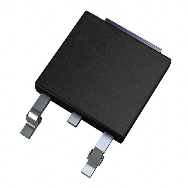
| 描述 | IC REG LDO 5V 0.8A TO252-3 |
| 产品分类 | |
| 品牌 | Texas Instruments |
| 数据手册 | |
| 产品图片 |
|
| 产品型号 | LM1117IDTX-5.0 |
| rohs | 含铅 / 不符合限制有害物质指令(RoHS)规范要求 |
| 产品系列 | - |
| 供应商器件封装 | TO-252-3 |
| 其它名称 | *LM1117IDTX-5.0 |
| 包装 | 剪切带 (CT) |
| 安装类型 | 表面贴装 |
| 封装/外壳 | TO-252-3,DPak(2 引线+接片),SC-63 |
| 工作温度 | -40°C ~ 125°C |
| 标准包装 | 1 |
| 电压-跌落(典型值) | 1.2V @ 800mA |
| 电压-输入 | 最高 15V |
| 电压-输出 | 5V |
| 电流-输出 | 800mA |
| 电流-限制(最小值) | 800mA |
| 稳压器拓扑 | 正,固定式 |
| 稳压器数 | 1 |


- 商务部:美国ITC正式对集成电路等产品启动337调查
- 曝三星4nm工艺存在良率问题 高通将骁龙8 Gen1或转产台积电
- 太阳诱电将投资9.5亿元在常州建新厂生产MLCC 预计2023年完工
- 英特尔发布欧洲新工厂建设计划 深化IDM 2.0 战略
- 台积电先进制程称霸业界 有大客户加持明年业绩稳了
- 达到5530亿美元!SIA预计今年全球半导体销售额将创下新高
- 英特尔拟将自动驾驶子公司Mobileye上市 估值或超500亿美元
- 三星加码芯片和SET,合并消费电子和移动部门,撤换高东真等 CEO
- 三星电子宣布重大人事变动 还合并消费电子和移动部门
- 海关总署:前11个月进口集成电路产品价值2.52万亿元 增长14.8%


PDF Datasheet 数据手册内容提取
Product Sample & Technical Tools & Support & Reference Folder Buy Documents Software Community Design LM1117 SNOS412N–FEBRUARY2000–REVISEDJANUARY2016 LM1117 800-mA Low-Dropout Linear Regulator 1 Features 3 Description • Availablein1.8V,2.5V,3.3V,5V,and The LM1117 is a low dropout voltage regulator with a 1 dropoutof1.2Vat800mAofloadcurrent. AdjustableVersions • Space-SavingSOT-223andWSONPackages The LM1117 is available in an adjustable version, which can set the output voltage from 1.25 to 13.8 V • CurrentLimitingandThermalProtection with only two external resistors. In addition, it is • OutputCurrent800mA available in five fixed voltages, 1.8 V, 2.5 V, 3.3 V, • LineRegulation0.2%(Maximum) and5V. • LoadRegulation0.4%(Maximum) The LM1117 offers current limiting and thermal • TemperatureRange shutdown. Its circuit includes a Zener trimmed bandgap reference to assure output voltage accuracy – LM1117:0°Cto125°C towithin ±1%. – LM1117I: −40°Cto125°C A minimum of 10-µF tantalum capacitor is required at 2 Applications the output to improve the transient response and stability. • PostRegulatorforSwitchingDC–DCConverter • HighEfficiencyLinearRegulators DeviceInformation(1) • BatteryChargers PARTNUMBER PACKAGE BODYSIZE(NOM) • PortableInstrumentation SOT-223(4) 6.50mm×3.50mm • ActiveSCSITerminationRegulator TO-220(3) 14.986mm×10.16mm LM1117, TO-252(3) 6.58mm×6.10mm LM1117I WSON(8) 4.00mm×4.00mm TO-263(3) 10.18mm×8.41mm (1) For all available packages, see the orderable addendum at theendofthedatasheet. AdjustableOutputRegulator 1 An IMPORTANT NOTICE at the end of this data sheet addresses availability, warranty, changes, use in safety-critical applications, intellectualpropertymattersandotherimportantdisclaimers.PRODUCTIONDATA.
LM1117 SNOS412N–FEBRUARY2000–REVISEDJANUARY2016 www.ti.com Table of Contents 1 Features.................................................................. 1 7.3 FeatureDescription.................................................11 2 Applications........................................................... 1 7.4 DeviceFunctionalModes........................................12 3 Description............................................................. 1 8 ApplicationandImplementation........................ 14 4 RevisionHistory..................................................... 2 8.1 ApplicationInformation............................................14 8.2 TypicalApplication..................................................14 5 PinConfigurationandFunctions......................... 3 8.3 SystemExamples...................................................16 6 Specifications......................................................... 4 9 PowerSupplyRecommendations...................... 17 6.1 AbsoluteMaximumRatings......................................4 10 Layout................................................................... 17 6.2 ESDRatings..............................................................4 6.3 RecommendedOperatingConditions.......................4 10.1 LayoutGuidelines.................................................17 6.4 ThermalInformation..................................................4 10.2 LayoutExample....................................................21 6.5 LM1117ElectricalCharacteristics.............................5 11 DeviceandDocumentationSupport................. 22 6.6 LM1117IElectricalCharacteristics............................7 11.1 CommunityResources..........................................22 6.7 TypicalCharacteristics..............................................9 11.2 Trademarks...........................................................22 7 DetailedDescription............................................ 11 11.3 ElectrostaticDischargeCaution............................22 7.1 Overview.................................................................11 11.4 Glossary................................................................22 7.2 FunctionalBlockDiagram.......................................11 12 Mechanical,Packaging,andOrderable Information........................................................... 22 4 Revision History NOTE:Pagenumbersforpreviousrevisionsmaydifferfrompagenumbersinthecurrentversion. ChangesfromRevisionM(March2013)toRevisionN Page • AddedPinConfigurationandFunctionssection,ESDRatingstable,FeatureDescriptionsection,DeviceFunctional Modes,ApplicationandImplementationsection,PowerSupplyRecommendationssection,Layoutsection,Device andDocumentationSupportsection,andMechanical,Packaging,andOrderableInformationsection .............................. 1 • RemovedLM1117-N-2.85optionafterpartbecameinactive................................................................................................. 1 • RemovedTO-263PinoutSideViewimage ........................................................................................................................... 3 ChangesfromRevisionL(July2012)toRevisionM Page • ChangedlayoutofNationalDataSheettoTIformat........................................................................................................... 16 2 SubmitDocumentationFeedback Copyright©2000–2016,TexasInstrumentsIncorporated ProductFolderLinks:LM1117
LM1117 www.ti.com SNOS412N–FEBRUARY2000–REVISEDJANUARY2016 5 Pin Configuration and Functions DCYPackage 4-PinSOT KTTPackage TopView 3-PinTO-263 TopView NDEPackage NDPPackage 3-PinTO-220 3-PinTO-252 TopView TopView NGNPackage 8-PinWSON TopView ADJ/GND 1 8 NOT CONNECTED VIN 2 7 VOUT VOUT VIN 3 6 VOUT VIN 4 5 VOUT WhenusingtheWSONpackage Pins2,3and4mustbeconnectedtogetherand Pins5,6and7mustbeconnectedtogether PinFunctions PIN I/O DESCRIPTION NAME TO-252 WSON SOT-223 TO-263 TO-220 Adjustpinforadjustableoutputoption.Groundpinforfixed ADJ/GND 1 1 1 1 1 — outputoption. V 3 2,3,4 3 3 3 I Inputvoltagepinfortheregulator IN 5,6,7, V 2,TAB 2,4 2,TAB 2,TAB O Outputvoltagepinfortheregulator OUT TAB Copyright©2000–2016,TexasInstrumentsIncorporated SubmitDocumentationFeedback 3 ProductFolderLinks:LM1117
LM1117 SNOS412N–FEBRUARY2000–REVISEDJANUARY2016 www.ti.com 6 Specifications 6.1 Absolute Maximum Ratings overoperatingfree-airtemperaturerange(unlessotherwisenoted)(1) MIN MAX UNIT MaximumInputVoltage(V toGND) 20 V IN PowerDissipation(2) InternallyLimited JunctionTemperature(T)(2) 150 °C J TO-220(T)Package,10s 260 LeadTemperature °C SOT-223(MP)Package,4s 260 StorageTemperature,T –65 150 °C stg (1) StressesbeyondthoselistedunderAbsoluteMaximumRatingsmaycausepermanentdamagetothedevice.Thesearestressratings only,whichdonotimplyfunctionaloperationofthedeviceattheseoranyotherconditionsbeyondthoseindicatedunderRecommended OperatingConditions.Exposuretoabsolute-maximum-ratedconditionsforextendedperiodsmayaffectdevicereliability. (2) ThemaximumpowerdissipationisafunctionofT ,R ,andT .Themaximumallowablepowerdissipationatanyambient J(max) θJA A temperatureisP =(T –T )/R .AllnumbersapplyforpackagessoldereddirectlyintoaPCB. D J(max) A θJA 6.2 ESD Ratings VALUE UNIT V Electrostaticdischarge Human-bodymodel(HBM),perANSI/ESDA/JEDECJS-001(1) ±2000 V (ESD) (1) JEDECdocumentJEP155statesthat500-VHBMallowssafemanufacturingwithastandardESDcontrolprocess.Pinslistedas±2000 Vmayactuallyhavehigherperformance. 6.3 Recommended Operating Conditions overoperatingfree-airtemperaturerange(unlessotherwisenoted) MIN MAX UNIT InputVoltage(V toGND) 15 V IN LM1117 0 125 °C JunctionTemperature(T)(1) J LM1117I −40 125 (1) ThemaximumpowerdissipationisafunctionofT ,R ,andT .Themaximumallowablepowerdissipationatanyambient J(max) θJA A temperatureisP =(T –T )/R .AllnumbersapplyforpackagessoldereddirectlyintoaPCB. D J(max) A θJA 6.4 Thermal Information LM1117,LM1117I DCY NDE NDP NGN KTT THERMALMETRIC(1) UNIT (SOT-223) (TO-220) (TO-252) (WSON) (TO-263) 4PINS 3PINS 3PINS 8PINS 3PINS RθJA Junction-to-ambientthermalresistance 61.6 23.8 45.1 39.3 41.3 °C/W RθJC(top) Junction-to-case(top)thermalresistance 42.5 16.6 52.1 31.4 44.1 °C/W RθJB Junction-to-boardthermalresistance 10.4 5.3 29.8 16.5 24.2 °C/W ψJT Junction-to-topcharacterizationparameter 2.9 3.1 4.5 0.3 10.9 °C/W ψJB Junction-to-boardcharacterizationparameter 10.3 5.3 29.4 16.7 23.2 °C/W RθJC(bot) Junction-to-case(bottom)thermalresistance — 1.5 1.3 5.6 1.3 °C/W (1) Formoreinformationabouttraditionalandnewthermalmetrics,seetheSemiconductorandICPackageThermalMetricsapplication report,SPRA953. 4 SubmitDocumentationFeedback Copyright©2000–2016,TexasInstrumentsIncorporated ProductFolderLinks:LM1117
LM1117 www.ti.com SNOS412N–FEBRUARY2000–REVISEDJANUARY2016 6.5 LM1117 Electrical Characteristics unlessotherwisespecified,T =25°C. J PARAMETER TESTCONDITIONS MIN(1) TYP(2) MAX(1) UNIT LM1117-ADJ 1.238 1.25 1.262 IOUT=10mA,VIN–VOUT=2V,TJ=25°C VREF ReferenceVoltage LM1117-ADJ TJ=25°C 1.25 V 10mA≤IOUT≤800mA,1.4V≤ overthejunctiontemperaturerange VIN–VOUT≤10V 0°Cto125°C 1.225 1.27 LM1117-1.8 1.782 1.8 1.818 IOUT=10mA,VIN=3.8V,TJ=25°C LM1117-1.8 TJ=25°C 1.8 V 0≤IOUT≤800mA,3.2V≤VIN≤ overthejunctiontemperaturerange 10V 0°Cto125°C 1.746 1.854 LM1117-2.5 2.475 2.5 2.525 IOUT=10mA,VIN=4.5V,TJ=25°C LM1117-2.5 TJ=25°C 2.5 V 0≤IOUT≤800mA,3.9V≤VIN≤ overthejunctiontemperaturerange 10V 0°Cto125°C 2.45 2.55 VOUT OutputVoltage LM1117-3.3 3.267 3.3 3.333 IOUT=10mA,VIN=5VTJ=25°C LM1117-3.3 TJ=25°C 3.3 V 0≤IOUT≤800mA,4.75V≤VIN≤ overthejunctiontemperaturerange 10V 0°Cto125°C 3.235 3.365 LM1117-5.0 4.95 5 5.05 IOUT=10mA,VIN=7V,TJ=25°C LM1117-5.0 TJ=25°C 5 V 0≤IOUT≤800mA,6.5V≤VIN≤ overthejunctiontemperaturerange 12V 0°Cto125°C 4.9 5.1 LM1117-ADJ TJ=25°C 0.035% IOUT=10mA,1.5V≤VIN-VOUT≤ overthejunctiontemperaturerange 13.75V 0°Cto125°C 0.2% TJ=25°C 1 LM1117-1.8 IOUT=0mA,3.2V≤VIN≤10V overthejunctiontemperaturerange 6 mV 0°Cto125°C TJ=25°C 1 ΔVOUT LineRegulation(3) LIOMUT11=107-m2.A5,3.9V≤VIN≤10V overthejunctiontemperaturerange 6 mV 0°Cto125°C TJ=25°C 1 LM1117-3.3 IOUT=0mA,4.75V≤VIN≤15V overthejunctiontemperaturerange 6 mV 0°Cto125°C TJ=25°C 1 LM1117-5.0 IOUT=0mA,6.5V≤VIN≤15V overthejunctiontemperaturerange 10 mV 0°Cto125°C LM1117-ADJ TJ=25°C 0.2% VIN–VOUT=3V,10≤IOUT≤800 overthejunctiontemperaturerange mA 0°Cto125°C 0.4% TJ=25°C 1 LM1117-1.8 VIN=3.2V,0≤IOUT≤800mA overthejunctiontemperaturerange 10 mV 0°Cto125°C TJ=25°C 1 ΔVOUT LoadRegulation(3) LVMIN1=1137.9-2V.5,0≤IOUT≤800mA overthejunctiontemperaturerange 10 mV 0°Cto125°C TJ=25°C 1 LM1117-3.3 VIN=4.75V,0≤IOUT≤800mA overthejunctiontemperaturerange 10 mV 0°Cto125°C TJ=25°C 1 LM1117-5.0 VIN=6.5V,0≤IOUT≤800mA overthejunctiontemperaturerange 15 mV 0°Cto125°C (1) Alllimitsareensuredbytestingorstatisticalanalysis. (2) TypicalValuesrepresentthemostlikelyparametricnormal. (3) Loadandlineregulationaremeasuredatconstantjunctionroomtemperature. Copyright©2000–2016,TexasInstrumentsIncorporated SubmitDocumentationFeedback 5 ProductFolderLinks:LM1117
LM1117 SNOS412N–FEBRUARY2000–REVISEDJANUARY2016 www.ti.com LM1117 Electrical Characteristics (continued) unlessotherwisespecified,T =25°C. J PARAMETER TESTCONDITIONS MIN(1) TYP(2) MAX(1) UNIT TJ=25°C 1.1 IOUT=100mA overthejunctiontemperaturerange V 1.2 0°Cto125°C TJ=25°C 1.15 VIN–V DropoutVoltage(4) IOUT=500mA overthejunctiontemperaturerange V OUT 1.25 0°Cto125°C TJ=25°C 1.2 IOUT=800mA overthejunctiontemperaturerange V 1.3 0°Cto125°C ILIMIT CurrentLimit VIN–VOUT=5V,TJ=25°C 800 1200 1500 mA TJ=25°C 1.7 MinimumLoad LM1117-ADJ Current(5) VIN=15V overthejunctiontemperaturerange 5 mA 0°Cto125°C TJ=25°C 5 LM1117-1.8 VIN≤15V overthejunctiontemperaturerange 10 mA 0°Cto125°C TJ=25°C 5 LM1117-2.5 VIN≤15V overthejunctiontemperaturerange 10 mA 0°Cto125°C QuiescentCurrent TJ=25°C 5 LM1117-3.3 VIN≤15V overthejunctiontemperaturerange 10 mA 0°Cto125°C TJ=25°C 5 LM1117-5.0 VIN≤15V overthejunctiontemperaturerange 10 mA 0°Cto125°C ThermalRegulation TA=25°C,30-mspulse 0.01 0.1 %/W TJ=25°C 75 RippleRegulation fVRIVPPRLIEPP=LE1=210VHPzP,VIN–VOUT=3 overthejunctiontemperaturerange 60 dB 0°Cto125°C TJ=25°C 60 AdjustPinCurrent μA overthejunctiontemperaturerange0°Cto125°C 120 TJ=25°C 0.2 ACdhjaunsgtePinCurrent 110.4≤VIO≤UVTI≤N8–0V0OmUTA≤,10V overthejunctiontemperaturerange 5 µA 0°Cto125°C TemperatureStability 0.5% LongTermStability TA=125°C,1000Hrs 0.3% RMSOutputNoise (%ofVOUT),10Hz≤f≤10kHz 0.003% (4) Thedropoutvoltageistheinput/outputdifferentialatwhichthecircuitceasestoregulateagainstfurtherreductionininputvoltage.Itis measuredwhentheoutputvoltagehasdropped100mVfromthenominalvalueobtainedatV =V +1.5V. IN OUT (5) Theminimumoutputcurrentrequiredtomaintainregulation. 6 SubmitDocumentationFeedback Copyright©2000–2016,TexasInstrumentsIncorporated ProductFolderLinks:LM1117
LM1117 www.ti.com SNOS412N–FEBRUARY2000–REVISEDJANUARY2016 6.6 LM1117I Electrical Characteristics unlessotherwisespecified,T =25°C. J PARAMETER TESTCONDITIONS MIN(1) TYP(2) MAX(1) UNIT LM1117I-ADJ 1.238 1.25 1.262 I =10mA,V –V =2V,T =25°C OUT IN OUT J T =25°C 1.25 VREF ReferenceVoltage LM1117I-ADJ J V 10mA≤I ≤800mA,1.4V≤ overthejunction OUT V –V ≤10V temperaturerange 1.2 1.29 IN OUT –40°Cto125°C LM1117I-3.3 3.267 3.3 3.333 I =10mA,V =5V,T =25°C OUT IN J T =25°C 3.3 LM1117I-3.3 J V 0≤I ≤800mA,4.75V≤V ≤ overthejunction OUT IN 10V temperaturerange 3.168 3.432 –40°Cto125°C V OutputVoltage OUT LM1117I-5.0 4.95 5 5.05 I =10mA,V =7V,T =25°C OUT IN J T =25°C 5 LM1117I-5.0 J V 0≤I ≤800mA,6.5V≤V ≤12 overthejunction OUT IN V temperaturerange 4.8 5.2 –40°Cto125°C T =25°C LM1117I-ADJ J 0.035% IOUT=10mA,1.5V≤VIN–VOUT≤ overthejunction 13.75V temperaturerange 0.3% –40°Cto125°C T =25°C 1 J ΔVOUT LineRegulation(3) LM1117I-3.3 overthejunction mV IOUT=0mA,4.75V≤VIN≤15V temperaturerange 10 –40°Cto125°C T =25°C 1 J LM1117I-5.0 overthejunction mV IOUT=0mA,6.5V≤VIN≤15V temperaturerange 15 –40°Cto125°C T =25°C 0.2% J LM1117I-ADJ V –V =3V,10≤I ≤800 overthejunction IN OUT OUT mA temperaturerange 0.5% –40°Cto125°C T =25°C 1 J ΔV LoadRegulation(3) LM1117I-3.3 overthejunction mV OUT VIN=4.75V,0≤IOUT≤800mA temperaturerange 15 –40°Cto125°C T =25°C 1 J LM1117I-5.0 overthejunction mV VIN=6.5V,0≤IOUT≤800mA temperaturerange 20 –40°Cto125°C (1) Alllimitsareensuredbytestingorstatisticalanalysis. (2) TypicalValuesrepresentthemostlikelyparametricnormal. (3) Loadandlineregulationaremeasuredatconstantjunctionroomtemperature. Copyright©2000–2016,TexasInstrumentsIncorporated SubmitDocumentationFeedback 7 ProductFolderLinks:LM1117
LM1117 SNOS412N–FEBRUARY2000–REVISEDJANUARY2016 www.ti.com LM1117I Electrical Characteristics (continued) unlessotherwisespecified,T =25°C. J PARAMETER TESTCONDITIONS MIN(1) TYP(2) MAX(1) UNIT T =25°C 1.1 J I =100mA overthejunction V OUT temperaturerange 1.3 –40°Cto125°C T =25°C 1.15 J V -V DropoutVoltage(4) I =500mA overthejunction V IN OUT OUT temperaturerange 1.35 –40°Cto125°C T =25°C 1.2 J I =800mA overthejunction V OUT temperaturerange 1.4 –40°Cto125°C I CurrentLimit V –V =5V,T =25°C 800 1200 1500 mA LIMIT IN OUT J T =25°C 1.7 J MCuinrirmenutm(5)Load LVMIN1=11175I-VADJ otevmerpethreatjuurnecrtaionnge 5 mA –40°Cto125°C T =25°C 5 J LM1117I-3.3 overthejunction mA VIN≤15V temperaturerange 15 –40°Cto125°C QuiescentCurrent T =25°C 5 J LM1117I-5.0 overthejunction mA VIN≤15V temperaturerange 15 –40°Cto125°C ThermalRegulation T =25°C,30msPulse 0.01 0.1 %/W A T =25°C 75 J RippleRegulation fRIPPLE=120Hz,VIN–VOUT=3V overthejunction dB VRIPPLE=1VPP temperaturerange 60 –40°Cto125°C T =25°C 60 J AdjustPinCurrent μA overthejunctiontemperaturerange–40°Cto125°C 120 T =25°C 0.2 J AdjustPinCurrent 10≤IOUT≤800mA, overthejunction µA Change 1.4V≤VIN–VOUT≤10V temperaturerange 10 –40°Cto125°C Temperature 0.5% Stability LongTermStability T =125°C,1000Hrs 0.3% A RMSOutputNoise (%ofV ),10Hz≤f≤10kHz 0.003% OUT (4) Thedropoutvoltageistheinput/outputdifferentialatwhichthecircuitceasestoregulateagainstfurtherreductionininputvoltage.Itis measuredwhentheoutputvoltagehasdropped100mVfromthenominalvalueobtainedatV =V +1.5V. IN OUT (5) Theminimumoutputcurrentrequiredtomaintainregulation. 8 SubmitDocumentationFeedback Copyright©2000–2016,TexasInstrumentsIncorporated ProductFolderLinks:LM1117
LM1117 www.ti.com SNOS412N–FEBRUARY2000–REVISEDJANUARY2016 6.7 Typical Characteristics Figure1.DropoutVoltage(V –V ) Figure2.Short-CircuitCurrent IN OUT Figure3.LoadRegulation Figure4.LM1117-ADJRippleRejection Figure5.LM1117-ADJRippleRejectionvsCurrent Figure6.TemperatureStability Copyright©2000–2016,TexasInstrumentsIncorporated SubmitDocumentationFeedback 9 ProductFolderLinks:LM1117
LM1117 SNOS412N–FEBRUARY2000–REVISEDJANUARY2016 www.ti.com Typical Characteristics (continued) Figure7.AdjustPinCurrent Figure8.LM1117-5.0LoadTransientResponse Figure9.LM1117-5.0LineTransientResponse 10 SubmitDocumentationFeedback Copyright©2000–2016,TexasInstrumentsIncorporated ProductFolderLinks:LM1117
LM1117 www.ti.com SNOS412N–FEBRUARY2000–REVISEDJANUARY2016 7 Detailed Description 7.1 Overview The LM1117 adjustable version develops a 1.25V reference voltage, V , between the output and the adjust REF terminal. As shown in Figure 10, this voltage is applied across resistor R1 to generate a constant current I1. The current I from the adjust terminal could introduce error to the output. But since it is very small (60µA) ADJ compared with the I1 and very constant with line and load changes, the error can be ignored. The constant currentI1thenflowsthroughtheoutputsetresistorR2andsetstheoutputvoltagetothedesiredlevel. Forfixedvoltagedevices,R1andR2areintegratedinsidethedevices. Figure10. BasicAdjustableRegulator 7.2 Functional Block Diagram 7.3 Feature Description 7.3.1 LoadRegulation The LM1117 regulates the voltage that appears between its output and ground pins, or between its output and adjust pins. In some cases, line resistances can introduce errors to the voltage across the load. To obtain the bestloadregulation,afewprecautionsareneeded. Copyright©2000–2016,TexasInstrumentsIncorporated SubmitDocumentationFeedback 11 ProductFolderLinks:LM1117
LM1117 SNOS412N–FEBRUARY2000–REVISEDJANUARY2016 www.ti.com Feature Description (continued) Figure 11, shows a typical application using a fixed output regulator. The Rt1 and Rt2 are the line resistances. It is obvious that the V is less than the V by the sum of the voltage drops along the line resistances. In this LOAD OUT case, the load regulation seen at the R would be degraded from the data sheet specification. To improve LOAD this, the load should be tied directly to the output terminal on the positive side and directly tied to the ground terminalonthenegativeside. Figure11. TypicalApplicationUsingFixedOutputRegulator When the adjustable regulator is used (Figure 12), the best performance is obtained with the positive side of the resistorR1tieddirectlytotheoutputterminaloftheregulatorratherthanneartheload.Thiseliminateslinedrops fromappearingeffectivelyinserieswiththereferenceanddegradingregulation.Forexample,a5Vregulatorwith 0.05Ω resistance between the regulator and load will have a load regulation due to line resistance of 0.05Ω x I . L If R1 (=125Ω) is connected near the load, the effective line resistance will be 0.05Ω (1+R2/R1) or in this case, it is 4 times worse. In addition, the ground side of the resistor R2 can be returned near the ground of the load to provideremotegroundsensingandimproveloadregulation. Figure12. BestLoadRegulationUsingAdjustableOutputRegulator 7.4 Device Functional Modes 7.4.1 ProtectionDiodes Under normal operation, the LM1117 regulators do not need any protection diode. With the adjustable device, the internal resistance between the adjust and output terminals limits the current. No diode is needed to divert the current around the regulator even with capacitor on the adjust terminal. The adjust pin can take a transient signalof±25Vwithrespecttotheoutputvoltagewithoutdamagingthedevice. When a output capacitor is connected to a regulator and the input is shorted to ground, the output capacitor will discharge into the output of the regulator. The discharge current depends on the value of the capacitor, the output voltage of the regulator, and rate of decrease of V . In the LM1117 regulators, the internal diode between IN the output and input pins can withstand microsecond surge currents of 10A to 20A. With an extremely large outputcapacitor(≥1000 µF),andwithinputinstantaneouslyshortedtoground,theregulatorcouldbedamaged. In this case, an external diode is recommended between the output and input pins to protect the regulator, as showninFigure13. 12 SubmitDocumentationFeedback Copyright©2000–2016,TexasInstrumentsIncorporated ProductFolderLinks:LM1117
LM1117 www.ti.com SNOS412N–FEBRUARY2000–REVISEDJANUARY2016 Device Functional Modes (continued) Figure13. RegulatorWithProtectionDiode Copyright©2000–2016,TexasInstrumentsIncorporated SubmitDocumentationFeedback 13 ProductFolderLinks:LM1117
LM1117 SNOS412N–FEBRUARY2000–REVISEDJANUARY2016 www.ti.com 8 Application and Implementation NOTE Information in the following applications sections is not part of the TI component specification, and TI does not warrant its accuracy or completeness. TI’s customers are responsible for determining suitability of components for their purposes. Customers should validateandtesttheirdesignimplementationtoconfirmsystemfunctionality. 8.1 Application Information The LM1117 is a versatile and high performance linear regulator with a wide temperature range and tight line/load regulation operation. An output capacitor is required to further improve transient response and stability. For the adjustable option, the ADJ pin can also be bypassed to achieve very high ripple-rejection ratios. The LM1117 is versatile in its applications, including its uses as a post regulator for DC/DC converters, battery chargers,andmicroprocessorsupplies. 8.2 Typical Application Figure14. 1.25-Vto10-VAdjustableRegulatorWithImprovedRippleRejection 8.2.1 DesignRequirements The device component count is very minimal, employing two resistors as part of a voltage divider circuit and an output capacitor for load regulation. A 10-μF tantalum on the input is a suitable input capacitor for almost all applications. An optional bypass capacitor across R2 can also be used to improve PSRR. See Recommended OperatingConditionsformoreinformation. 8.2.2 DetailedDesignProcedure The output voltage is set based on the selection of the two resistors, R1 and R2, as shown in Figure 14. For detailsoncapacitorselection,refertoExternalCapacitors. 8.2.2.1 ExternalCapacitors 8.2.2.1.1 InputBypassCapacitor An input capacitor is recommended. A 10-µF tantalum on the input is a suitable input capacitor for almost all applications. 14 SubmitDocumentationFeedback Copyright©2000–2016,TexasInstrumentsIncorporated ProductFolderLinks:LM1117
LM1117 www.ti.com SNOS412N–FEBRUARY2000–REVISEDJANUARY2016 Typical Application (continued) 8.2.2.1.2 AdjustTerminalBypassCapacitor The adjust terminal can be bypassed to ground with a bypass capacitor (C ) to improve ripple rejection. This ADJ bypass capacitor prevents ripple from being amplified as the output voltage is increased. At any ripple frequency, theimpedanceoftheC shouldbelessthanR1topreventtheripplefrombeingamplified: ADJ 1/(2π×f ×C )<R1 (1) RIPPLE ADJ The R1 is the resistor between the output and the adjust pin. Its value is normally in the range of 100-200Ω. For example,withR1=124Ω andf =120Hz,theC shouldbe >11µF. RIPPLE ADJ 8.2.2.1.3 OutputCapacitor The output capacitor is critical in maintaining regulator stability, and must meet the required conditions for both minimum amount of capacitance and equivalent series resistance (ESR). The minimum output capacitance required by the LM1117 is 10 µF, if a tantalum capacitor is used. Any increase of the output capacitance will merely improve the loop stability and transient response. The ESR of the output capacitor should range between 0.3 Ω to 22 Ω. In the case of the adjustable regulator, when the C is used, a larger output capacitance (22-µF ADJ tantalum)isrequired. 8.2.3 ApplicationCurve As shown in Figure 15, the dropout voltage will vary with output current and temperature. Care should be taken during design to ensure the dropout voltage requirement is met across the entire operating temperature and outputcurrentrange. Figure15. DropoutVoltage(V –V ) IN OUT Copyright©2000–2016,TexasInstrumentsIncorporated SubmitDocumentationFeedback 15 ProductFolderLinks:LM1117
LM1117 SNOS412N–FEBRUARY2000–REVISEDJANUARY2016 www.ti.com 8.3 System Examples Several circuits can be realized with the LM1117. The circuit diagrams in this section demonstrate multiple systemexamplesthatcanbeutilizedinmanyapplications. Figure16.FixedOutputRegulator Figure17.AdjustingOutputofFixedRegulators Figure18.RegulatorWithReference Figure19.5-VLogicRegulatorWithElectronic Shutdown* Figure20. BatteryBacked-UpRegulatedSupply Figure21. LowDropoutNegativeSupply 16 SubmitDocumentationFeedback Copyright©2000–2016,TexasInstrumentsIncorporated ProductFolderLinks:LM1117
LM1117 www.ti.com SNOS412N–FEBRUARY2000–REVISEDJANUARY2016 9 Power Supply Recommendations The input supply to the LM1117 must be kept at a voltage level such that its maximum rating is not exceeded. The minimum dropout voltage must also be met with extra headroom when possible to keep the LM1117 in regulation. An input capacitor is recommended. For more information regarding capacitor selection, refer to ExternalCapacitors. 10 Layout 10.1 Layout Guidelines Some layout guidelines must be followed to ensure proper regulation of the output voltage with minimum noise. Traces carrying the load current must be wide to reduce the amount of parasitic trace inductance and the feedback loop from V to ADJ must be kept as short as possible. To improve PSRR, a bypass capacitor can OUT beplacedattheADJpinandmustbelocatedascloseaspossibletotheIC.IncaseswhenV shortstoground, IN an external diode must be placed from V to V to divert the surge current from the output capacitor and OUT IN protecttheIC.ThediodemustbeplacedclosetothecorrespondingICpinstoincreasetheireffectiveness. 10.1.1 HeatsinkRequirements When an integrated circuit operates with an appreciable current, its junction temperature is elevated. It is important to quantify its thermal limits in order to achieve acceptable performance and reliability. This limit is determined by summing the individual parts consisting of a series of temperature rises from the semiconductor junction to the operating environment. A one-dimensional steady-state model of conduction heat transfer is demonstrated in Figure 22. The heat generated at the device junction flows through the die to the die attach pad, through the lead frame to the surrounding case material, to the printed circuit board, and eventually to the ambient environment. Below is a list of variables that may affect the thermal resistance and in turn the need for a heatsink. Table1.ComponentandApplicationVariables R (COMPONENTVARIABLES) R (APPLICATIONVARIABLES) θJC θJA LeadframeSizeandMaterial MountingPadSize,Material,andLocation No.ofConductionPins PlacementofMountingPad DieSize PCBSizeandMaterial DieAttachMaterial TracesLengthandWidth MoldingCompoundSizeandMaterial AdjacentHeatSources VolumeofAir AmbientTemperatue ShapeofMountingPad Thecasetemperatureismeasuredatthepointwheretheleadscontactwiththemountingpadsurface Figure22. Cross-SectionalViewofIntegratedCircuitMountedonaPrintedCircuitBoard Copyright©2000–2016,TexasInstrumentsIncorporated SubmitDocumentationFeedback 17 ProductFolderLinks:LM1117
LM1117 SNOS412N–FEBRUARY2000–REVISEDJANUARY2016 www.ti.com The LM1117 regulators have internal thermal shutdown to protect the device from over-heating. Under all possible operating conditions, the junction temperature of the LM1117 must be within the range of 0°C to 125°C. Aheatsinkmayberequireddependingonthemaximumpowerdissipationandmaximumambienttemperatureof the application. To determine if a heatsink is needed, the power dissipated by the regulator, P , must be D calculated: I =I +I (2) IN L G P =(V -V )I +V I (3) D IN OUT L ING Figure23showsthevoltagesandcurrentswhicharepresentinthecircuit. Figure23. PowerDissipationDiagram Thenextparameterwhichmustbecalculatedisthemaximumallowabletemperaturerise,T (max): R T (max)=T(max)-T (max) R J A where • T(max)isthemaximumallowablejunctiontemperature(125°C)whichwillbeencounteredintheapplication J • T (max)isthemaximumambienttemperaturewhichwillbeencounteredintheapplication (4) A Using the calculated values for T (max) and P , the maximum allowable value for the junction-to-ambient R D thermalresistance(R )canbecalculated: θJA R =T (max)/P (5) θJA R D Forthemaximumallowablevalueforθ ,refertotheThermalInformationtable. JA As a design aid, Table 2 shows the value of the θ of SOT-223 and TO-252 for different heatsink area. JA Figure24andFigure25reflectsthesametestresultsaswhatareintheTable2 Figure 26 and Figure 27 shows the maximum allowable power dissipation vs. ambient temperature for the SOT- 223 and TO-252 device. Figure 28 and Figure 29 shows the maximum allowable power dissipation vs. copper area (in2) for the SOT-223 and TO-252 devices. Please see AN1028 for power enhancement techniques to be usedwithSOT-223andTO-252packages. Application Note AN-1187 (SNOA401) discusses improved thermal performance and power dissipation for the WSON. Table2.R DifferentHeatsinkArea θJA LAYOUT COPPERAREA THERMALRESISTANCE TopSide(in2)(1) BottomSide(in2) (θ ,°C/W)SOT-223 (θ ,°C/W)TO-252 JA JA 1 0.0123 0 136 103 2 0.066 0 123 87 3 0.3 0 84 60 4 0.53 0 75 54 5 0.76 0 69 52 6 1 0 66 47 7 0 0.2 115 84 8 0 0.4 98 70 9 0 0.6 89 63 10 0 0.8 82 57 (1) Tabofdeviceattachedtotopsidecopper 18 SubmitDocumentationFeedback Copyright©2000–2016,TexasInstrumentsIncorporated ProductFolderLinks:LM1117
LM1117 www.ti.com SNOS412N–FEBRUARY2000–REVISEDJANUARY2016 Table2.R DifferentHeatsinkArea(continued) θJA LAYOUT COPPERAREA THERMALRESISTANCE 11 0 1 79 57 12 0.066 0.066 125 89 13 0.175 0.175 93 72 14 0.284 0.284 83 61 15 0.392 0.392 75 55 16 0.5 0.5 70 53 Figure24.R vs1-ozCopperAreaforSOT-223 Figure25. R vs2-ozCopperAreaforTO-252 θJA θJA Figure26.MaximumAllowablePowerDissipationvs Figure27.MaximumAllowablePowerDissipationvs AmbientTemperatureforSOT-223 AmbientTemperatureforTO-252 Figure28. MaximumAllowablePowerDissipationvs1-oz Figure29.MaximumAllowablePowerDissipationvs2-oz CopperAreaforSOT-223 CopperAreaforTO-252 Copyright©2000–2016,TexasInstrumentsIncorporated SubmitDocumentationFeedback 19 ProductFolderLinks:LM1117
LM1117 SNOS412N–FEBRUARY2000–REVISEDJANUARY2016 www.ti.com Figure30. TopViewoftheThermalTestPatterninActualScale Figure31. BottomViewoftheThermalTestPatterninActualScale 20 SubmitDocumentationFeedback Copyright©2000–2016,TexasInstrumentsIncorporated ProductFolderLinks:LM1117
LM1117 www.ti.com SNOS412N–FEBRUARY2000–REVISEDJANUARY2016 10.2 Layout Example Figure32. LayoutExample(SOT-223) Copyright©2000–2016,TexasInstrumentsIncorporated SubmitDocumentationFeedback 21 ProductFolderLinks:LM1117
LM1117 SNOS412N–FEBRUARY2000–REVISEDJANUARY2016 www.ti.com 11 Device and Documentation Support 11.1 Community Resources The following links connect to TI community resources. Linked contents are provided "AS IS" by the respective contributors. They do not constitute TI specifications and do not necessarily reflect TI's views; see TI's Terms of Use. TIE2E™OnlineCommunity TI'sEngineer-to-Engineer(E2E)Community.Createdtofostercollaboration amongengineers.Ate2e.ti.com,youcanaskquestions,shareknowledge,exploreideasandhelp solveproblemswithfellowengineers. DesignSupport TI'sDesignSupport QuicklyfindhelpfulE2Eforumsalongwithdesignsupporttoolsand contactinformationfortechnicalsupport. 11.2 Trademarks E2EisatrademarkofTexasInstruments. Allothertrademarksarethepropertyoftheirrespectiveowners. 11.3 Electrostatic Discharge Caution Thesedeviceshavelimitedbuilt-inESDprotection.Theleadsshouldbeshortedtogetherorthedeviceplacedinconductivefoam duringstorageorhandlingtopreventelectrostaticdamagetotheMOSgates. 11.4 Glossary SLYZ022—TIGlossary. Thisglossarylistsandexplainsterms,acronyms,anddefinitions. 12 Mechanical, Packaging, and Orderable Information The following pages include mechanical, packaging, and orderable information. This information is the most current data available for the designated devices. This data is subject to change without notice and revision of thisdocument.Forbrowser-basedversionsofthisdatasheet,refertotheleft-handnavigation. 22 SubmitDocumentationFeedback Copyright©2000–2016,TexasInstrumentsIncorporated ProductFolderLinks:LM1117
PACKAGE OPTION ADDENDUM www.ti.com 3-Feb-2016 PACKAGING INFORMATION Orderable Device Status Package Type Package Pins Package Eco Plan Lead/Ball Finish MSL Peak Temp Op Temp (°C) Device Marking Samples (1) Drawing Qty (2) (6) (3) (4/5) LM1117DT-1.8/NOPB ACTIVE TO-252 NDP 3 75 Green (RoHS CU SN Level-2-260C-1 YEAR 0 to 125 LM1117 & no Sb/Br) DT-1.8 LM1117DT-2.5/NOPB ACTIVE TO-252 NDP 3 75 Green (RoHS CU SN Level-2-260C-1 YEAR 0 to 125 LM1117 & no Sb/Br) DT-2.5 LM1117DT-3.3/NOPB ACTIVE TO-252 NDP 3 75 Green (RoHS CU SN Level-2-260C-1 YEAR 0 to 125 LM1117 & no Sb/Br) DT-3.3 LM1117DT-5.0/NOPB ACTIVE TO-252 NDP 3 75 Green (RoHS CU SN Level-2-260C-1 YEAR 0 to 125 LM1117 & no Sb/Br) DT-5.0 LM1117DT-ADJ/NOPB ACTIVE TO-252 NDP 3 75 Green (RoHS CU SN Level-2-260C-1 YEAR 0 to 125 LM1117 & no Sb/Br) DT-ADJ LM1117DTX-1.8/NOPB ACTIVE TO-252 NDP 3 2500 Green (RoHS CU SN Level-2-260C-1 YEAR 0 to 125 LM1117 & no Sb/Br) DT-1.8 LM1117DTX-2.5/NOPB ACTIVE TO-252 NDP 3 2500 Green (RoHS CU SN Level-2-260C-1 YEAR 0 to 125 LM1117 & no Sb/Br) DT-2.5 LM1117DTX-3.3/NOPB ACTIVE TO-252 NDP 3 2500 Green (RoHS CU SN Level-2-260C-1 YEAR 0 to 125 LM1117 & no Sb/Br) DT-3.3 LM1117DTX-5.0/NOPB ACTIVE TO-252 NDP 3 2500 Green (RoHS CU SN Level-2-260C-1 YEAR 0 to 125 LM1117 & no Sb/Br) DT-5.0 LM1117DTX-ADJ/NOPB ACTIVE TO-252 NDP 3 2500 Green (RoHS CU SN Level-2-260C-1 YEAR 0 to 125 LM1117 & no Sb/Br) DT-ADJ LM1117IDT-3.3/NOPB ACTIVE TO-252 NDP 3 75 Green (RoHS CU SN Level-2-260C-1 YEAR -40 to 125 LM1117 & no Sb/Br) IDT-3.3 LM1117IDT-5.0/NOPB ACTIVE TO-252 NDP 3 75 Green (RoHS CU SN Level-2-260C-1 YEAR -40 to 125 LM1117 & no Sb/Br) IDT-5.0 LM1117IDT-ADJ/NOPB ACTIVE TO-252 NDP 3 75 Green (RoHS CU SN Level-2-260C-1 YEAR -40 to 125 LM1117 & no Sb/Br) IDT-ADJ LM1117IDTX-3.3/NOPB ACTIVE TO-252 NDP 3 2500 Green (RoHS CU SN Level-2-260C-1 YEAR -40 to 125 LM1117 & no Sb/Br) IDT-3.3 LM1117IDTX-5.0/NOPB ACTIVE TO-252 NDP 3 2500 Green (RoHS CU SN Level-2-260C-1 YEAR -40 to 125 LM1117 & no Sb/Br) IDT-5.0 LM1117IDTX-ADJ/NOPB ACTIVE TO-252 NDP 3 2500 Green (RoHS CU SN Level-2-260C-1 YEAR -40 to 125 LM1117 & no Sb/Br) IDT-ADJ LM1117ILD-ADJ/NOPB ACTIVE WSON NGN 8 1000 Green (RoHS CU SN Level-3-260C-168 HR -40 to 125 1117IAD & no Sb/Br) Addendum-Page 1
PACKAGE OPTION ADDENDUM www.ti.com 3-Feb-2016 Orderable Device Status Package Type Package Pins Package Eco Plan Lead/Ball Finish MSL Peak Temp Op Temp (°C) Device Marking Samples (1) Drawing Qty (2) (6) (3) (4/5) LM1117IMP-3.3/NOPB ACTIVE SOT-223 DCY 4 1000 Green (RoHS CU SN Level-1-260C-UNLIM -40 to 125 N05B & no Sb/Br) LM1117IMP-5.0/NOPB ACTIVE SOT-223 DCY 4 1000 Green (RoHS CU SN Level-1-260C-UNLIM -40 to 125 N06B & no Sb/Br) LM1117IMP-ADJ/NOPB ACTIVE SOT-223 DCY 4 1000 Green (RoHS CU SN Level-1-260C-UNLIM -40 to 125 N03B & no Sb/Br) LM1117IMPX-3.3/NOPB ACTIVE SOT-223 DCY 4 2000 Green (RoHS CU SN Level-1-260C-UNLIM -40 to 125 N05B & no Sb/Br) LM1117IMPX-5.0/NOPB ACTIVE SOT-223 DCY 4 2000 Green (RoHS CU SN Level-1-260C-UNLIM -40 to 125 N06B & no Sb/Br) LM1117IMPX-ADJ/NOPB ACTIVE SOT-223 DCY 4 2000 Green (RoHS CU SN Level-1-260C-UNLIM -40 to 125 N03B & no Sb/Br) LM1117LD-1.8/NOPB ACTIVE WSON NGN 8 1000 Green (RoHS CU SN Level-3-260C-168 HR 0 to 125 1117-18 & no Sb/Br) LM1117LD-2.5/NOPB ACTIVE WSON NGN 8 1000 Green (RoHS CU SN Level-3-260C-168 HR 0 to 125 1117-25 & no Sb/Br) LM1117LD-3.3/NOPB ACTIVE WSON NGN 8 1000 Green (RoHS CU SN Level-3-260C-168 HR 0 to 125 1117-33 & no Sb/Br) LM1117LD-ADJ/NOPB ACTIVE WSON NGN 8 1000 Green (RoHS CU SN Level-3-260C-168 HR 0 to 125 1117ADJ & no Sb/Br) LM1117LDX-1.8 NRND WSON NGN 8 4500 TBD Call TI Call TI 0 to 125 1117-18 LM1117LDX-1.8/NOPB ACTIVE WSON NGN 8 4500 Green (RoHS CU SN Level-3-260C-168 HR 0 to 125 1117-18 & no Sb/Br) LM1117LDX-ADJ/NOPB ACTIVE WSON NGN 8 4500 Green (RoHS CU SN Level-3-260C-168 HR 0 to 125 1117ADJ & no Sb/Br) LM1117MP-1.8/NOPB ACTIVE SOT-223 DCY 4 1000 Green (RoHS CU SN Level-1-260C-UNLIM 0 to 125 N12A & no Sb/Br) LM1117MP-2.5/NOPB ACTIVE SOT-223 DCY 4 1000 Green (RoHS CU SN Level-1-260C-UNLIM 0 to 125 N13A & no Sb/Br) LM1117MP-3.3/NOPB ACTIVE SOT-223 DCY 4 1000 Green (RoHS CU SN Level-1-260C-UNLIM 0 to 125 N05A & no Sb/Br) LM1117MP-5.0/NOPB ACTIVE SOT-223 DCY 4 1000 Green (RoHS CU SN Level-1-260C-UNLIM 0 to 125 N06A & no Sb/Br) LM1117MP-ADJ/NOPB ACTIVE SOT-223 DCY 4 1000 Green (RoHS CU SN Level-1-260C-UNLIM 0 to 125 N03A & no Sb/Br) Addendum-Page 2
PACKAGE OPTION ADDENDUM www.ti.com 3-Feb-2016 Orderable Device Status Package Type Package Pins Package Eco Plan Lead/Ball Finish MSL Peak Temp Op Temp (°C) Device Marking Samples (1) Drawing Qty (2) (6) (3) (4/5) LM1117MPX-1.8/NOPB ACTIVE SOT-223 DCY 4 2000 Green (RoHS CU SN Level-1-260C-UNLIM 0 to 125 N12A & no Sb/Br) LM1117MPX-2.5/NOPB ACTIVE SOT-223 DCY 4 2000 Green (RoHS CU SN Level-1-260C-UNLIM 0 to 125 N13A & no Sb/Br) LM1117MPX-3.3 ACTIVE SOT-223 DCY 4 2000 TBD Call TI Call TI N05A LM1117MPX-3.3/NOPB ACTIVE SOT-223 DCY 4 2000 Green (RoHS CU SN Level-1-260C-UNLIM 0 to 125 N05A & no Sb/Br) LM1117MPX-5.0/NOPB ACTIVE SOT-223 DCY 4 2000 Green (RoHS CU SN Level-1-260C-UNLIM 0 to 125 N06A & no Sb/Br) LM1117MPX-ADJ/NOPB ACTIVE SOT-223 DCY 4 2000 Green (RoHS CU SN Level-1-260C-UNLIM 0 to 125 N03A & no Sb/Br) LM1117S-ADJ/NOPB ACTIVE DDPAK/ KTT 3 45 Pb-Free (RoHS CU SN Level-3-245C-168 HR 0 to 125 LM1117S TO-263 Exempt) ADJ LM1117SX-3.3/NOPB ACTIVE DDPAK/ KTT 3 500 Pb-Free (RoHS CU SN Level-3-245C-168 HR 0 to 125 LM1117S TO-263 Exempt) 3.3 LM1117SX-5.0/NOPB ACTIVE DDPAK/ KTT 3 500 Pb-Free (RoHS CU SN Level-3-245C-168 HR 0 to 125 LM1117S TO-263 Exempt) 5.0 LM1117SX-ADJ/NOPB ACTIVE DDPAK/ KTT 3 500 Pb-Free (RoHS CU SN Level-3-245C-168 HR 0 to 125 LM1117S TO-263 Exempt) ADJ LM1117T-2.5/NOPB ACTIVE TO-220 NDE 3 45 Green (RoHS CU SN Level-1-NA-UNLIM 0 to 125 LM1117T & no Sb/Br) 2.5 LM1117T-3.3/NOPB ACTIVE TO-220 NDE 3 45 Green (RoHS CU SN Level-1-NA-UNLIM 0 to 125 LM1117T & no Sb/Br) 3.3 LM1117T-5.0/NOPB ACTIVE TO-220 NDE 3 45 Green (RoHS CU SN Level-1-NA-UNLIM 0 to 125 LM1117T & no Sb/Br) 5.0 LM1117T-ADJ/NOPB ACTIVE TO-220 NDE 3 45 Green (RoHS CU SN Level-1-NA-UNLIM 0 to 125 LM1117T & no Sb/Br) ADJ (1) The marketing status values are defined as follows: ACTIVE: Product device recommended for new designs. LIFEBUY: TI has announced that the device will be discontinued, and a lifetime-buy period is in effect. NRND: Not recommended for new designs. Device is in production to support existing customers, but TI does not recommend using this part in a new design. PREVIEW: Device has been announced but is not in production. Samples may or may not be available. OBSOLETE: TI has discontinued the production of the device. Addendum-Page 3
PACKAGE OPTION ADDENDUM www.ti.com 3-Feb-2016 (2) Eco Plan - The planned eco-friendly classification: Pb-Free (RoHS), Pb-Free (RoHS Exempt), or Green (RoHS & no Sb/Br) - please check http://www.ti.com/productcontent for the latest availability information and additional product content details. TBD: The Pb-Free/Green conversion plan has not been defined. Pb-Free (RoHS): TI's terms "Lead-Free" or "Pb-Free" mean semiconductor products that are compatible with the current RoHS requirements for all 6 substances, including the requirement that lead not exceed 0.1% by weight in homogeneous materials. Where designed to be soldered at high temperatures, TI Pb-Free products are suitable for use in specified lead-free processes. Pb-Free (RoHS Exempt): This component has a RoHS exemption for either 1) lead-based flip-chip solder bumps used between the die and package, or 2) lead-based die adhesive used between the die and leadframe. The component is otherwise considered Pb-Free (RoHS compatible) as defined above. Green (RoHS & no Sb/Br): TI defines "Green" to mean Pb-Free (RoHS compatible), and free of Bromine (Br) and Antimony (Sb) based flame retardants (Br or Sb do not exceed 0.1% by weight in homogeneous material) (3) MSL, Peak Temp. - The Moisture Sensitivity Level rating according to the JEDEC industry standard classifications, and peak solder temperature. (4) There may be additional marking, which relates to the logo, the lot trace code information, or the environmental category on the device. (5) Multiple Device Markings will be inside parentheses. Only one Device Marking contained in parentheses and separated by a "~" will appear on a device. If a line is indented then it is a continuation of the previous line and the two combined represent the entire Device Marking for that device. (6) Lead/Ball Finish - Orderable Devices may have multiple material finish options. Finish options are separated by a vertical ruled line. Lead/Ball Finish values may wrap to two lines if the finish value exceeds the maximum column width. Important Information and Disclaimer:The information provided on this page represents TI's knowledge and belief as of the date that it is provided. TI bases its knowledge and belief on information provided by third parties, and makes no representation or warranty as to the accuracy of such information. Efforts are underway to better integrate information from third parties. TI has taken and continues to take reasonable steps to provide representative and accurate information but may not have conducted destructive testing or chemical analysis on incoming materials and chemicals. TI and TI suppliers consider certain information to be proprietary, and thus CAS numbers and other limited information may not be available for release. In no event shall TI's liability arising out of such information exceed the total purchase price of the TI part(s) at issue in this document sold by TI to Customer on an annual basis. Addendum-Page 4
PACKAGE MATERIALS INFORMATION www.ti.com 20-Sep-2016 TAPE AND REEL INFORMATION *Alldimensionsarenominal Device Package Package Pins SPQ Reel Reel A0 B0 K0 P1 W Pin1 Type Drawing Diameter Width (mm) (mm) (mm) (mm) (mm) Quadrant (mm) W1(mm) LM1117DTX-1.8/NOPB TO-252 NDP 3 2500 330.0 16.4 6.9 10.5 2.7 8.0 16.0 Q2 LM1117DTX-2.5/NOPB TO-252 NDP 3 2500 330.0 16.4 6.9 10.5 2.7 8.0 16.0 Q2 LM1117DTX-3.3/NOPB TO-252 NDP 3 2500 330.0 16.4 6.9 10.5 2.7 8.0 16.0 Q2 LM1117DTX-5.0/NOPB TO-252 NDP 3 2500 330.0 16.4 6.9 10.5 2.7 8.0 16.0 Q2 LM1117DTX-ADJ/NOPB TO-252 NDP 3 2500 330.0 16.4 6.9 10.5 2.7 8.0 16.0 Q2 LM1117IDTX-3.3/NOPB TO-252 NDP 3 2500 330.0 16.4 6.9 10.5 2.7 8.0 16.0 Q2 LM1117IDTX-5.0/NOPB TO-252 NDP 3 2500 330.0 16.4 6.9 10.5 2.7 8.0 16.0 Q2 LM1117IDTX-ADJ/NOPB TO-252 NDP 3 2500 330.0 16.4 6.9 10.5 2.7 8.0 16.0 Q2 LM1117ILD-ADJ/NOPB WSON NGN 8 1000 178.0 12.4 4.3 4.3 1.3 8.0 12.0 Q1 LM1117IMP-3.3/NOPB SOT-223 DCY 4 1000 330.0 16.4 7.0 7.5 2.2 12.0 16.0 Q3 LM1117IMP-5.0/NOPB SOT-223 DCY 4 1000 330.0 16.4 7.0 7.5 2.2 12.0 16.0 Q3 LM1117IMP-ADJ/NOPB SOT-223 DCY 4 1000 330.0 16.4 7.0 7.5 2.2 12.0 16.0 Q3 LM1117IMPX-3.3/NOPB SOT-223 DCY 4 2000 330.0 16.4 7.0 7.5 2.2 12.0 16.0 Q3 LM1117IMPX-5.0/NOPB SOT-223 DCY 4 2000 330.0 16.4 7.0 7.5 2.2 12.0 16.0 Q3 LM1117IMPX-ADJ/NOPB SOT-223 DCY 4 2000 330.0 16.4 7.0 7.5 2.2 12.0 16.0 Q3 LM1117LD-1.8/NOPB WSON NGN 8 1000 178.0 12.4 4.3 4.3 1.3 8.0 12.0 Q1 LM1117LD-2.5/NOPB WSON NGN 8 1000 178.0 12.4 4.3 4.3 1.3 8.0 12.0 Q1 LM1117LD-3.3/NOPB WSON NGN 8 1000 178.0 12.4 4.3 4.3 1.3 8.0 12.0 Q1 PackMaterials-Page1
PACKAGE MATERIALS INFORMATION www.ti.com 20-Sep-2016 Device Package Package Pins SPQ Reel Reel A0 B0 K0 P1 W Pin1 Type Drawing Diameter Width (mm) (mm) (mm) (mm) (mm) Quadrant (mm) W1(mm) LM1117LD-ADJ/NOPB WSON NGN 8 1000 178.0 12.4 4.3 4.3 1.3 8.0 12.0 Q1 LM1117LDX-1.8 WSON NGN 8 4500 330.0 12.4 4.3 4.3 1.3 8.0 12.0 Q1 LM1117LDX-1.8/NOPB WSON NGN 8 4500 330.0 12.4 4.3 4.3 1.3 8.0 12.0 Q1 LM1117LDX-ADJ/NOPB WSON NGN 8 4500 330.0 12.4 4.3 4.3 1.3 8.0 12.0 Q1 LM1117MP-1.8/NOPB SOT-223 DCY 4 1000 330.0 16.4 7.0 7.5 2.2 12.0 16.0 Q3 LM1117MP-2.5/NOPB SOT-223 DCY 4 1000 330.0 16.4 7.0 7.5 2.2 12.0 16.0 Q3 LM1117MP-3.3/NOPB SOT-223 DCY 4 1000 330.0 16.4 7.0 7.5 2.2 12.0 16.0 Q3 LM1117MP-5.0/NOPB SOT-223 DCY 4 1000 330.0 16.4 7.0 7.5 2.2 12.0 16.0 Q3 LM1117MP-ADJ/NOPB SOT-223 DCY 4 1000 330.0 16.4 7.0 7.5 2.2 12.0 16.0 Q3 LM1117MPX-1.8/NOPB SOT-223 DCY 4 2000 330.0 16.4 7.0 7.5 2.2 12.0 16.0 Q3 LM1117MPX-2.5/NOPB SOT-223 DCY 4 2000 330.0 16.4 7.0 7.5 2.2 12.0 16.0 Q3 LM1117MPX-3.3 SOT-223 DCY 4 2000 330.0 16.4 7.0 7.5 2.2 12.0 16.0 Q3 LM1117MPX-3.3/NOPB SOT-223 DCY 4 2000 330.0 16.4 7.0 7.5 2.2 12.0 16.0 Q3 LM1117MPX-5.0/NOPB SOT-223 DCY 4 2000 330.0 16.4 7.0 7.5 2.2 12.0 16.0 Q3 LM1117MPX-ADJ/NOPB SOT-223 DCY 4 2000 330.0 16.4 7.0 7.5 2.2 12.0 16.0 Q3 LM1117SX-3.3/NOPB DDPAK/ KTT 3 500 330.0 24.4 10.75 14.85 5.0 16.0 24.0 Q2 TO-263 LM1117SX-5.0/NOPB DDPAK/ KTT 3 500 330.0 24.4 10.75 14.85 5.0 16.0 24.0 Q2 TO-263 LM1117SX-ADJ/NOPB DDPAK/ KTT 3 500 330.0 24.4 10.75 14.85 5.0 16.0 24.0 Q2 TO-263 PackMaterials-Page2
PACKAGE MATERIALS INFORMATION www.ti.com 20-Sep-2016 *Alldimensionsarenominal Device PackageType PackageDrawing Pins SPQ Length(mm) Width(mm) Height(mm) LM1117DTX-1.8/NOPB TO-252 NDP 3 2500 367.0 367.0 38.0 LM1117DTX-2.5/NOPB TO-252 NDP 3 2500 367.0 367.0 38.0 LM1117DTX-3.3/NOPB TO-252 NDP 3 2500 367.0 367.0 38.0 LM1117DTX-5.0/NOPB TO-252 NDP 3 2500 367.0 367.0 38.0 LM1117DTX-ADJ/NOPB TO-252 NDP 3 2500 367.0 367.0 38.0 LM1117IDTX-3.3/NOPB TO-252 NDP 3 2500 367.0 367.0 38.0 LM1117IDTX-5.0/NOPB TO-252 NDP 3 2500 367.0 367.0 38.0 LM1117IDTX-ADJ/NOPB TO-252 NDP 3 2500 367.0 367.0 38.0 LM1117ILD-ADJ/NOPB WSON NGN 8 1000 210.0 185.0 35.0 LM1117IMP-3.3/NOPB SOT-223 DCY 4 1000 367.0 367.0 35.0 LM1117IMP-5.0/NOPB SOT-223 DCY 4 1000 367.0 367.0 35.0 LM1117IMP-ADJ/NOPB SOT-223 DCY 4 1000 367.0 367.0 35.0 LM1117IMPX-3.3/NOPB SOT-223 DCY 4 2000 367.0 367.0 35.0 LM1117IMPX-5.0/NOPB SOT-223 DCY 4 2000 367.0 367.0 35.0 LM1117IMPX-ADJ/NOPB SOT-223 DCY 4 2000 367.0 367.0 35.0 LM1117LD-1.8/NOPB WSON NGN 8 1000 210.0 185.0 35.0 LM1117LD-2.5/NOPB WSON NGN 8 1000 210.0 185.0 35.0 LM1117LD-3.3/NOPB WSON NGN 8 1000 210.0 185.0 35.0 LM1117LD-ADJ/NOPB WSON NGN 8 1000 210.0 185.0 35.0 LM1117LDX-1.8 WSON NGN 8 4500 367.0 367.0 35.0 LM1117LDX-1.8/NOPB WSON NGN 8 4500 367.0 367.0 35.0 LM1117LDX-ADJ/NOPB WSON NGN 8 4500 367.0 367.0 35.0 LM1117MP-1.8/NOPB SOT-223 DCY 4 1000 367.0 367.0 35.0 LM1117MP-2.5/NOPB SOT-223 DCY 4 1000 367.0 367.0 35.0 LM1117MP-3.3/NOPB SOT-223 DCY 4 1000 367.0 367.0 35.0 LM1117MP-5.0/NOPB SOT-223 DCY 4 1000 367.0 367.0 35.0 LM1117MP-ADJ/NOPB SOT-223 DCY 4 1000 367.0 367.0 35.0 LM1117MPX-1.8/NOPB SOT-223 DCY 4 2000 367.0 367.0 35.0 LM1117MPX-2.5/NOPB SOT-223 DCY 4 2000 367.0 367.0 35.0 LM1117MPX-3.3 SOT-223 DCY 4 2000 367.0 367.0 35.0 LM1117MPX-3.3/NOPB SOT-223 DCY 4 2000 367.0 367.0 35.0 LM1117MPX-5.0/NOPB SOT-223 DCY 4 2000 367.0 367.0 35.0 LM1117MPX-ADJ/NOPB SOT-223 DCY 4 2000 367.0 367.0 35.0 LM1117SX-3.3/NOPB DDPAK/TO-263 KTT 3 500 367.0 367.0 45.0 LM1117SX-5.0/NOPB DDPAK/TO-263 KTT 3 500 367.0 367.0 45.0 LM1117SX-ADJ/NOPB DDPAK/TO-263 KTT 3 500 367.0 367.0 45.0 PackMaterials-Page3
MECHANICAL DATA NDE0003B www.ti.com
MECHANICAL DATA NDP0003B TD03B (Rev F) www.ti.com
MECHANICAL DATA MPDS094A – APRIL 2001 – REVISED JUNE 2002 DCY (R-PDSO-G4) PLASTIC SMALL-OUTLINE 6,70 (0.264) 6,30 (0.248) 3,10 (0.122) 2,90 (0.114) 4 0,10 (0.004) M 7,30 (0.287) 3,70 (0.146) 6,70 (0.264) 3,30 (0.130) Gauge Plane 1 2 3 0,84 (0.033) 0°–10° 0,25 (0.010) 2,30 (0.091) 0,66 (0.026) 0,10 (0.004) M 4,60 (0.181) 0,75 (0.030) MIN 1,70 (0.067) 1,80 (0.071) MAX 1,50 (0.059) 0,35 (0.014) 0,23 (0.009) Seating Plane 0,10 (0.0040) 0,08 (0.003) 0,02 (0.0008) 4202506/B 06/2002 NOTES: A. All linear dimensions are in millimeters (inches). B. This drawing is subject to change without notice. C. Body dimensions do not include mold flash or protrusion. D. Falls within JEDEC TO-261 Variation AA. • POST OFFICE BOX 655303 DALLAS, TEXAS 75265
None
MECHANICAL DATA NGN0008A LDC08A (Rev B) www.ti.com
MECHANICAL DATA KTT0003B TS3B (Rev F) BOTTOM SIDE OF PACKAGE www.ti.com
IMPORTANTNOTICE TexasInstrumentsIncorporatedanditssubsidiaries(TI)reservetherighttomakecorrections,enhancements,improvementsandother changestoitssemiconductorproductsandservicesperJESD46,latestissue,andtodiscontinueanyproductorserviceperJESD48,latest issue.Buyersshouldobtainthelatestrelevantinformationbeforeplacingordersandshouldverifythatsuchinformationiscurrentand complete.Allsemiconductorproducts(alsoreferredtohereinas“components”)aresoldsubjecttoTI’stermsandconditionsofsale suppliedatthetimeoforderacknowledgment. TIwarrantsperformanceofitscomponentstothespecificationsapplicableatthetimeofsale,inaccordancewiththewarrantyinTI’sterms andconditionsofsaleofsemiconductorproducts.TestingandotherqualitycontroltechniquesareusedtotheextentTIdeemsnecessary tosupportthiswarranty.Exceptwheremandatedbyapplicablelaw,testingofallparametersofeachcomponentisnotnecessarily performed. TIassumesnoliabilityforapplicationsassistanceorthedesignofBuyers’products.Buyersareresponsiblefortheirproductsand applicationsusingTIcomponents.TominimizetherisksassociatedwithBuyers’productsandapplications,Buyersshouldprovide adequatedesignandoperatingsafeguards. TIdoesnotwarrantorrepresentthatanylicense,eitherexpressorimplied,isgrantedunderanypatentright,copyright,maskworkright,or otherintellectualpropertyrightrelatingtoanycombination,machine,orprocessinwhichTIcomponentsorservicesareused.Information publishedbyTIregardingthird-partyproductsorservicesdoesnotconstitutealicensetousesuchproductsorservicesorawarrantyor endorsementthereof.Useofsuchinformationmayrequirealicensefromathirdpartyunderthepatentsorotherintellectualpropertyofthe thirdparty,oralicensefromTIunderthepatentsorotherintellectualpropertyofTI. ReproductionofsignificantportionsofTIinformationinTIdatabooksordatasheetsispermissibleonlyifreproductioniswithoutalteration andisaccompaniedbyallassociatedwarranties,conditions,limitations,andnotices.TIisnotresponsibleorliableforsuchaltered documentation.Informationofthirdpartiesmaybesubjecttoadditionalrestrictions. ResaleofTIcomponentsorserviceswithstatementsdifferentfromorbeyondtheparametersstatedbyTIforthatcomponentorservice voidsallexpressandanyimpliedwarrantiesfortheassociatedTIcomponentorserviceandisanunfairanddeceptivebusinesspractice. TIisnotresponsibleorliableforanysuchstatements. Buyeracknowledgesandagreesthatitissolelyresponsibleforcompliancewithalllegal,regulatoryandsafety-relatedrequirements concerningitsproducts,andanyuseofTIcomponentsinitsapplications,notwithstandinganyapplications-relatedinformationorsupport thatmaybeprovidedbyTI.Buyerrepresentsandagreesthatithasallthenecessaryexpertisetocreateandimplementsafeguardswhich anticipatedangerousconsequencesoffailures,monitorfailuresandtheirconsequences,lessenthelikelihoodoffailuresthatmightcause harmandtakeappropriateremedialactions.BuyerwillfullyindemnifyTIanditsrepresentativesagainstanydamagesarisingoutoftheuse ofanyTIcomponentsinsafety-criticalapplications. Insomecases,TIcomponentsmaybepromotedspecificallytofacilitatesafety-relatedapplications.Withsuchcomponents,TI’sgoalisto helpenablecustomerstodesignandcreatetheirownend-productsolutionsthatmeetapplicablefunctionalsafetystandardsand requirements.Nonetheless,suchcomponentsaresubjecttotheseterms. NoTIcomponentsareauthorizedforuseinFDAClassIII(orsimilarlife-criticalmedicalequipment)unlessauthorizedofficersoftheparties haveexecutedaspecialagreementspecificallygoverningsuchuse. OnlythoseTIcomponentswhichTIhasspecificallydesignatedasmilitarygradeor“enhancedplastic”aredesignedandintendedforusein military/aerospaceapplicationsorenvironments.BuyeracknowledgesandagreesthatanymilitaryoraerospaceuseofTIcomponents whichhavenotbeensodesignatedissolelyattheBuyer'srisk,andthatBuyerissolelyresponsibleforcompliancewithalllegaland regulatoryrequirementsinconnectionwithsuchuse. TIhasspecificallydesignatedcertaincomponentsasmeetingISO/TS16949requirements,mainlyforautomotiveuse.Inanycaseofuseof non-designatedproducts,TIwillnotberesponsibleforanyfailuretomeetISO/TS16949. Products Applications Audio www.ti.com/audio AutomotiveandTransportation www.ti.com/automotive Amplifiers amplifier.ti.com CommunicationsandTelecom www.ti.com/communications DataConverters dataconverter.ti.com ComputersandPeripherals www.ti.com/computers DLP®Products www.dlp.com ConsumerElectronics www.ti.com/consumer-apps DSP dsp.ti.com EnergyandLighting www.ti.com/energy ClocksandTimers www.ti.com/clocks Industrial www.ti.com/industrial Interface interface.ti.com Medical www.ti.com/medical Logic logic.ti.com Security www.ti.com/security PowerMgmt power.ti.com Space,AvionicsandDefense www.ti.com/space-avionics-defense Microcontrollers microcontroller.ti.com VideoandImaging www.ti.com/video RFID www.ti-rfid.com OMAPApplicationsProcessors www.ti.com/omap TIE2ECommunity e2e.ti.com WirelessConnectivity www.ti.com/wirelessconnectivity MailingAddress:TexasInstruments,PostOfficeBox655303,Dallas,Texas75265 Copyright©2016,TexasInstrumentsIncorporated