ICGOO在线商城 > 集成电路(IC) > PMIC - 稳压器 - 线性 > TPS79718DCKT
 Datasheet下载
- 型号: TPS79718DCKT
- 制造商: Texas Instruments
- 库位|库存: xxxx|xxxx
- 要求:
| 数量阶梯 | 香港交货 | 国内含税 |
| +xxxx | $xxxx | ¥xxxx |
查看当月历史价格
查看今年历史价格
TPS79718DCKT产品简介:
ICGOO电子元器件商城为您提供TPS79718DCKT由Texas Instruments设计生产,在icgoo商城现货销售,并且可以通过原厂、代理商等渠道进行代购。 TPS79718DCKT价格参考。Texas InstrumentsTPS79718DCKT封装/规格:PMIC - 稳压器 - 线性, Linear Voltage Regulator IC Positive Fixed 1 Output 1.8V 50mA SC-70-5。您可以下载TPS79718DCKT参考资料、Datasheet数据手册功能说明书,资料中有TPS79718DCKT 详细功能的应用电路图电压和使用方法及教程。
Texas Instruments(德州仪器)的TPS79718DCKT是一款PMIC(电源管理集成电路),具体分类为线性稳压器。它广泛应用于需要稳定、低噪声电源输出的电子设备中,适用于多种应用场景。

 1. 便携式电子产品
TPS79718DCKT常用于便携式电子设备,如智能手机、平板电脑、可穿戴设备等。这些设备对电源的要求非常严格,尤其是在待机和低功耗模式下,需要稳定的电压输出以确保系统的正常运行。TPS79718DCKT能够提供高效的低压差稳压功能,帮助延长电池寿命并减少发热。

 2. 通信设备
在通信设备中,如路由器、交换机、无线模块等,TPS79718DCKT可以为射频(RF)电路、基带处理器和其他关键组件提供干净、稳定的电源。其低噪声特性有助于提高通信质量,减少信号干扰,确保数据传输的可靠性和稳定性。

 3. 工业自动化
在工业自动化领域,TPS79718DCKT可用于各种传感器、控制器和执行器的电源管理。由于工业环境中可能存在较大的电磁干扰,TPS79718DCKT的低噪声和高稳定性特性使其成为理想选择,能够确保系统在恶劣环境下仍能保持精确的工作状态。

 4. 医疗设备
对于医疗设备,如便携式医疗仪器、监护仪、血糖仪等,TPS79718DCKT提供了可靠的电源解决方案。医疗设备对电源的精度和稳定性要求极高,TPS79718DCKT的低功耗和高精度特性能够满足这些需求,同时其小尺寸封装也有助于节省宝贵的PCB空间。

 5. 消费类电子产品
在消费类电子产品中,如智能家居设备、音频设备、摄像头等,TPS79718DCKT可以为微控制器、传感器和其他外围设备提供稳定的电源。其高效能和低功耗特性有助于提升产品的整体性能和用户体验。

总之,TPS79718DCKT凭借其出色的性能和可靠性,广泛应用于各类需要稳定电源输出的场景,特别适合对功耗、噪声和空间有严格要求的应用。
| 参数 | 数值 |
| 产品目录 | 集成电路 (IC)半导体 |
| 描述 | IC REG LDO 1.8V 50MA SC70-5低压差稳压器 10-mA 1.8-V LDO |
| 产品分类 | |
| 品牌 | Texas Instruments |
| 产品手册 | |
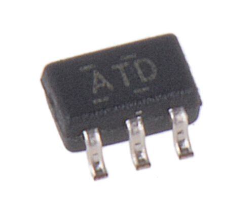
| 产品图片 |
|
| rohs | 符合RoHS无铅 / 符合限制有害物质指令(RoHS)规范要求 |
| 产品系列 | 电源管理 IC,低压差稳压器,Texas Instruments TPS79718DCKT- |
| 数据手册 | |
| 产品型号 | TPS79718DCKT |
| 产品种类 | 低压差稳压器 |
| 供应商器件封装 | SC-70-5 |
| 其它名称 | 296-27110-2 |
| 包装 | 带卷 (TR) |
| 单位重量 | 2.500 mg |
| 商标 | Texas Instruments |
| 安装类型 | 表面贴装 |
| 安装风格 | SMD/SMT |
| 封装 | Reel |
| 封装/外壳 | 6-TSSOP(5 引线),SC-88A,SOT-353 |
| 封装/箱体 | SC-70-5 |
| 工作温度 | -40°C ~ 85°C |
| 工厂包装数量 | 250 |
| 最大功率耗散 | 0.318 W |
| 最大工作温度 | + 85 C |
| 最大输入电压 | 5.5 V |
| 最小工作温度 | - 40 C |
| 最小输入电压 | + 1.8 V |
| 标准包装 | 250 |
| 电压-跌落(典型值) | - |
| 电压-输入 | 1.8 V ~ 5.5 V |
| 电压-输出 | 1.8V |
| 电压调节准确度 | 4 % |
| 电流-输出 | 50mA |
| 电流-限制(最小值) | - |
| 稳压器拓扑 | 正,固定式 |
| 稳压器数 | 1 |
| 系列 | TPS79718 |
| 线路调整率 | 0.15 % / V |
| 负载调节 | 5 mV |
| 输入偏压电流—最大 | 0.0012 mA |
| 输出电压 | 1.8 V |
| 输出电流 | 50 mA |
| 输出端数量 | 1 Output |
| 输出类型 | Fixed |
| 配用 | /product-detail/zh/TPS79733EVM/296-13595-ND/486553 |


- 商务部:美国ITC正式对集成电路等产品启动337调查
- 曝三星4nm工艺存在良率问题 高通将骁龙8 Gen1或转产台积电
- 太阳诱电将投资9.5亿元在常州建新厂生产MLCC 预计2023年完工
- 英特尔发布欧洲新工厂建设计划 深化IDM 2.0 战略
- 台积电先进制程称霸业界 有大客户加持明年业绩稳了
- 达到5530亿美元!SIA预计今年全球半导体销售额将创下新高
- 英特尔拟将自动驾驶子公司Mobileye上市 估值或超500亿美元
- 三星加码芯片和SET,合并消费电子和移动部门,撤换高东真等 CEO
- 三星电子宣布重大人事变动 还合并消费电子和移动部门
- 海关总署:前11个月进口集成电路产品价值2.52万亿元 增长14.8%


PDF Datasheet 数据手册内容提取
Product Sample & Technical Tools & Support & Folder Buy Documents Software Community TPS79718,TPS797285,TPS79730,TPS79733 SLVS332J–MARCH2001–REVISEDDECEMBER2016 TPS797xx Ultra-Low I , 50-mA Low-Dropout Linear Regulators Q With Power Good Output in SC70 Package 1 Features 3 Description • 50-mALow-DropoutRegulator The TPS797xx family of low-dropout voltage 1 regulators (LDOs) offers the benefits of low-dropout • Ultra-Low1.2-µAQuiescentCurrentat10mA voltage and ultra-low-power operation. The device is • 5-PinSC70(DCK)Package stable with any capacitor greater than 0.47-µF. • IntegratedPowerGoodOutput Therefore,implementationsofthisdevicerequirevery little board space due to the miniaturized packaging • StableWithAnyCapacitorGreaterThan0.47 µF and potentially small output capacitor. In addition, the • TypicalDropoutVoltageof105mVat10mA family includes an integrated open drain active-high (TPS79733) power good (PG) output. Intended for use in • Over-CurrentLimitation microcontroller-based, battery-powered applications, the TPS797xx family low dropout and ultra-low-power • OperatingJunctionTemperatureRangeof–40°C operation result in a significant increase in system to85°C battery operating life. The small packaging minimizes consumptionofboardspace. 2 Applications The device is enabled when the applied voltage • Battery-PoweredMicrocontrollersand exceeds the minimum input voltage. The usual PNP Microprocessors pass transistor has been replaced by a PMOS pass element. Because the PMOS pass element behaves as a low-value resistor, the dropout voltage is very low (typically, 105 mV at 10-mA of load current), and is directly proportional to the load current. The quiescent current is ultra-low (1.2-µA, typically) and is stable over the entire range of output load current (0 mA to 50 mA). When properly configured with a pullup resistor, the PG output can implement a power-onresetorlow-batteryindicator. DeviceInformation(1) PARTNUMBER PACKAGE BODYSIZE(NOM) TPS797xx SC70(5) 2.00mm×1.25mm (1) For all available packages, see the orderable addendum at theendofthedatasheet. GroundCurrentvsFree-AirTemperature 2.00 V = 4.3V I V = 3.3V 1.75 O DCK PACKAGE CO= 1mF (Top View) A) IO= 10mA nt (m 1.50 PG 1 5 OUT urre 1.25 C GND 2 nd ou 1.00 Gr NC 3 4 IN 0.75 0.50 -40 -15 10 35 60 85 Free-Air Temperature (°C) 1 An IMPORTANT NOTICE at the end of this data sheet addresses availability, warranty, changes, use in safety-critical applications, intellectualpropertymattersandotherimportantdisclaimers.PRODUCTIONDATA.
TPS79718,TPS797285,TPS79730,TPS79733 SLVS332J–MARCH2001–REVISEDDECEMBER2016 www.ti.com Table of Contents 1 Features.................................................................. 1 8 ApplicationandImplementation........................ 10 2 Applications........................................................... 1 8.1 ApplicationInformation............................................10 3 Description............................................................. 1 8.2 TypicalApplication .................................................10 4 RevisionHistory..................................................... 2 9 Power-SupplyRecommendations...................... 12 5 PinConfigurationandFunctions......................... 4 10 Layout................................................................... 12 6 Specifications......................................................... 4 10.1 LayoutGuidelines.................................................12 6.1 AbsoluteMaximumRatings......................................4 10.2 LayoutExample....................................................12 6.2 ESDRatings..............................................................4 10.3 PowerDissipationandJunctionTemperature......12 6.3 RecommendedOperatingConditions.......................5 11 DeviceandDocumentationSupport................. 13 6.4 ThermalInformation..................................................5 11.1 RelatedLinks........................................................13 6.5 ElectricalCharacteristics...........................................5 11.2 ReceivingNotificationofDocumentationUpdates13 6.6 TypicalCharacteristics..............................................7 11.3 CommunityResources..........................................13 7 DetailedDescription.............................................. 9 11.4 Trademarks...........................................................13 7.1 Overview...................................................................9 11.5 ElectrostaticDischargeCaution............................13 7.2 FunctionalBlockDiagram.........................................9 11.6 Glossary................................................................13 7.3 FeatureDescription...................................................9 12 Mechanical,Packaging,andOrderable Information........................................................... 13 7.4 DeviceFunctionalModes..........................................9 4 Revision History NOTE:Pagenumbersforpreviousrevisionsmaydifferfrompagenumbersinthecurrentversion. ChangesfromRevisionI(October2013)toRevisionJ Page • AddedESDRatingstable,FeatureDescriptionsection,DeviceFunctionalModes,ApplicationandImplementation section,PowerSupplyRecommendationssection,Layoutsection,DeviceandDocumentationSupportsection,and Mechanical,Packaging,andOrderableInformationsection.................................................................................................. 1 • DeletedDissipationRatingstable;seeThermalInformationtable......................................................................................... 4 • AddedThermalInformationtable........................................................................................................................................... 5 • ChangedLoadRegulationparameterunitFrom:mVTo:%/A............................................................................................... 5 • ChangedOutputSpectralNoiseDensityvsFrequencygraphY-axisunitFrom:nV/√HzTo:µV/√Hz.................................. 7 • ChangedIOUTxvaluesFrom:I To:I ............................................................................................................................... 9 CL SC ChangesfromRevisionH(April2012)toRevisionI Page • ChangedDropoutVoltagevsJunctionTemperaturegraphY-axisunitFrom:VTo:mV(typo)............................................ 8 ChangesfromRevisionG(November2009)toRevisionH Page • Deletedsentenceregardingthermalprotection.................................................................................................................... 12 ChangesfromRevisionF(May2009)toRevisionG Page • Changeddocumenttitle.......................................................................................................................................................... 1 • DeletedreferencestoSOT323packagethroughoutdocument............................................................................................. 1 • ChangedTestConditionsforElectricalCharacteristicstable................................................................................................ 5 • Changedoutputvoltageaccuracytestconditionsfrom10µA<I <10mAto1mA<I <10mA............................... 5 OUT OUT • Deletedlineregulationmaximumspecification...................................................................................................................... 5 • ChangedPGtripthresholdvoltagetestconditionsfromV decreasingtoV increasing;deletedminimumand OUT OUT maximumspecifications.......................................................................................................................................................... 5 • RevisedPGlowoutputlowvoltagetestconditions................................................................................................................ 5 2 SubmitDocumentationFeedback Copyright©2001–2016,TexasInstrumentsIncorporated ProductFolderLinks:TPS79718 TPS797285 TPS79730 TPS79733
TPS79718,TPS797285,TPS79730,TPS79733 www.ti.com SLVS332J–MARCH2001–REVISEDDECEMBER2016 • UpdatedPGleakagecurrenttestconditions.......................................................................................................................... 5 Copyright©2001–2016,TexasInstrumentsIncorporated SubmitDocumentationFeedback 3 ProductFolderLinks:TPS79718 TPS797285 TPS79730 TPS79733
TPS79718,TPS797285,TPS79730,TPS79733 SLVS332J–MARCH2001–REVISEDDECEMBER2016 www.ti.com 5 Pin Configuration and Functions DCKPackage 5-PinSC70 TopView PG 1 5 OUT GND 2 NC 3 4 IN PinFunctions PIN I/O DESCRIPTION NO. NAME ThePGpinforthefixedvoltageoptiondevicesisanopendrain,active-highoutputthat indicatesthestatusofV (outputoftheLDO).WhenV exceedsapproximately90%ofthe O O 1 PG O regulatedvoltage,PGgoestoahigh-impedancestate.PGgoestoalow-impedancestate whenV fallsbelowapproximately90%(thatis,overloadcondition)oftheregulatedvoltage. O TheopendrainoutputofthePGpinrequiresapullupresistor. 2 GND — Ground 3 NC — Noconnection 4 IN I TheINpinisthepower-supplyinputtothedevice. 5 OUT O TheOUTpinprovidestheregulatedoutputvoltageofthedevice. 6 Specifications 6.1 Absolute Maximum Ratings overoperatingfree-airtemperaturerange(unlessotherwisenoted) (1) MIN MAX UNIT Inputvoltage(2) –0.3 6 V Voltage Maximumdcoutputvoltage 4.9 V Current Peakoutputcurrent Internallylimited A Operatingvirtualjunctiontemperature,T –40 85 °C J Temperature Storagetemperature,T –65 150 °C stg (1) StressesbeyondthoselistedunderAbsoluteMaximumRatingsmaycausepermanentdamagetothedevice.Thesearestressratings only,whichdonotimplyfunctionaloperationofthedeviceattheseoranyotherconditionsbeyondthoseindicatedunderRecommended OperatingConditions.Exposuretoabsolute-maximum-ratedconditionsforextendedperiodsmayaffectdevicereliability. (2) Allvoltagevaluesarewithrespecttonetworkgroundpin. 6.2 ESD Ratings VALUE UNIT Human-bodymodel(HBM),perANSI/ESDA/JEDECJS-001(1) ±2000 V Electrostaticdischarge V (ESD) Charged-devicemodel(CDM),perJEDECspecificationJESD22-C101(2) ±500 (1) JEDECdocumentJEP155statesthat500-VHBMallowssafemanufacturingwithastandardESDcontrolprocess. (2) JEDECdocumentJEP157statesthat250-VCDMallowssafemanufacturingwithastandardESDcontrolprocess. 4 SubmitDocumentationFeedback Copyright©2001–2016,TexasInstrumentsIncorporated ProductFolderLinks:TPS79718 TPS797285 TPS79730 TPS79733
TPS79718,TPS797285,TPS79730,TPS79733 www.ti.com SLVS332J–MARCH2001–REVISEDDECEMBER2016 6.3 Recommended Operating Conditions overoperatingfree-airtemperaturerange(unlessotherwisenoted) MIN NOM MAX UNIT V Inputvoltage 1.8 5.5 V I V Outputvoltage 1.8 3.3 V O I Outputcurrent 0 50 mA O C Inputcapacitor 0 0.1 µF I C Outputcapacitor 0.47 1 µF O T Junctiontemperature –40 85 °C J 6.4 Thermal Information TPS797xx THERMALMETRIC(1) DCK(SC70) UNIT 5PINS R Junction-to-ambientthermalresistance 230.9 °C/W θJA R Junction-to-case(top)thermalresistance 98.3 °C/W θJC(top) R Junction-to-boardthermalresistance 70.7 °C/W θJB ψ Junction-to-topcharacterizationparameter 3.9 °C/W JT ψ Junction-to-boardcharacterizationparameter 70.1 °C/W JB R Junction-to-case(bottom)thermalresistance — °C/W θJC(bot) (1) Formoreinformationabouttraditionalandnewthermalmetrics,seeSemiconductorandICPackageThermalMetrics(SPRA953). 6.5 Electrical Characteristics overoperatingtemperaturerangeT =–40°Cto85°C,typicalvaluesareatT =25°C,V =V +0.5Vor2V(whicheveris J A I O(typ) greater);I =0.5mA,V ,V =V,andC =1µF(unlessotherwisenoted) O SET EN I O PARAMETER TESTCONDITIONS MIN TYP MAX UNIT I =3mA 1.8 5.5 V Inputvoltage(1) O V I I =10mA 2 5.5 O I Continuousoutputcurrent(2) 0 50 mA O V Outputvoltageaccuracy(3) VO+1V≤VI≤5.5V –4% 4% O 1mA<I <10mA O ΔV Lineregulation(3) V +1V≤V ≤5.5V 0.15% V O(ΔVI) O I ΔV Loadregulation 1µA<I <10mA 5% A O(ΔIO) O Dropoutvoltage(4),I =10mA TPS79730 110 200 V O mV (DO) VI=VO(NOM)–0.1V TPS79733 105 200 I Outputcurrentlimit V =0V 190 300 mA SC O I Groundpincurrent(3) I =10mA 1.2 2 µA (GND) O Power-supplyrejectionratio f=100Hz,C =10µF, PSRR O 50 dB (ripplerejection) I =10mA O BW=200kHzto100kHz, V Outputnoisevoltage(TPS79718) 600 µV n C =10µF,I =10mA RMS O O V MinimuminputvoltageforvalidPG V ≥0.8V,I =100µA 1.2 V Imin(PG) (PG) PG V PGtripthresholdvoltage V increasing 90% V IT OUT OUT V PGoutputlowvoltage V =1.4V,I =30µA,I =1mA 0.14 0.225 V OL(PG) I PG O V =5V,V =V +1V, I PGleakagecurrent (PG) I O 0.1 nA lkg(PG) I =1mA O (1) MinimumV =V +V ortheminimumvaluespecifiedhere,whicheverisgreater. I O (DO) (2) Continuousoutputcurrentislimitedbyinternalprotectioncircuitry,butitisnotrecommendedthatthedeviceoperateabovethis maximumforextendedperiodsoftime. (3) MinimumV isspecifiedin(1). I (4) V isnotmeasuredfortheTPS79718becauseminimumV >1.7V. (DO) I Copyright©2001–2016,TexasInstrumentsIncorporated SubmitDocumentationFeedback 5 ProductFolderLinks:TPS79718 TPS797285 TPS79730 TPS79733
TPS79718,TPS797285,TPS79730,TPS79733 SLVS332J–MARCH2001–REVISEDDECEMBER2016 www.ti.com V IN (1) V MIN t V OUT Threshold Voltage (2) V IT+ (2) VIT- t PG Output t NOTES: (1) V = V + V . MIN OUT DO (2) The PG trip voltage is typically 10% lower than the output voltage (90% VO). VIT+to VIT-is the hysteresis voltage. Figure1. TPS797xxPGTimingDiagram 6 SubmitDocumentationFeedback Copyright©2001–2016,TexasInstrumentsIncorporated ProductFolderLinks:TPS79718 TPS797285 TPS79730 TPS79733
TPS79718,TPS797285,TPS79730,TPS79733 www.ti.com SLVS332J–MARCH2001–REVISEDDECEMBER2016 6.6 Typical Characteristics overoperatingtemperaturerangeT =–40°Cto85°C,typicalvaluesareatT =25°C,V =V (typical)+0.5Vor2V J A I O (whicheverisgreater);I =0.5mA,V =V,andC =1µF(unlessotherwisenoted). O EN I O 3.465 1.890 V = 4.3V V = 2.8V 3.432 IN 1.872 IN C = 1mF C = 1mF OUT OUT 3.399 T = +25°C 1.854 T = +25°C A J V) 3.366 VOUT= 3.3V V) 1.836 VOUT= 1.8V ge ( 3.333 ge ( 1.818 a a olt 3.300 olt 1.800 V V ut 3.267 ut 1.782 p p Out 3.234 Out 1.764 3.201 1.746 3.168 1.728 3.135 1.710 0 10 20 30 40 50 0 10 20 30 40 50 Output Current (mA) Output Current (mA) Figure2.OutputVoltagevsOutputCurrent Figure3.OutputVoltagevsOutputCurrent 3.305 1.810 V = 4.3V V = 2.8V I = 10mA 3.300 CIONUT= 1mF IO= 1mA 1.805 CIONUT= 1mF O V = 3.3V V = 3.3V OUT OUT e (V) 3.295 IO= 10mA e (V) 1.800 IO= 1mA ag ag 1.795 Volt 3.290 Volt IO= 25mA ut ut 1.790 p p ut 3.285 ut O O 1.785 I = 25mA O 3.280 1.780 I = 50mA O I = 50mA O 3.275 1.775 -40 -15 10 35 60 85 -40 -15 10 35 60 85 Junction Temperature(°C) Junction Temperature(°C) Figure4.OutputVoltagevsJunctionTemperature Figure5.OutputVoltagevsJunctionTemperature 1.60 10 V = 4.3V )z V = 2.8 V IN H IN A)m 11..5400 VCOOUUTT== 31.m3FV IOUT= 50mA sity (V/μÖ 8 VCOOUUTT== 11.8m FV IOUT= 10 mA Ground Current ( 1111....32100000 IOUT= 25mA pectral Noise Den 64 IOUT= 1 mA 0.90 IOUT= 10mA put S 2 ut O 0.80 0 -40 -15 10 35 60 85 100 1k 10k 100k Free-Air Temperature (°C) Frequency (Hz) Figure6.GroundCurrentvsJunctionTemperature Figure7.OutputSpectralNoiseDensityvsFrequency Copyright©2001–2016,TexasInstrumentsIncorporated SubmitDocumentationFeedback 7 ProductFolderLinks:TPS79718 TPS797285 TPS79730 TPS79733
TPS79718,TPS797285,TPS79730,TPS79733 SLVS332J–MARCH2001–REVISEDDECEMBER2016 www.ti.com Typical Characteristics (continued) overoperatingtemperaturerangeT =–40°Cto85°C,typicalvaluesareatT =25°C,V =V (typical)+0.5Vor2V J A I O (whicheverisgreater);I =0.5mA,V =V,andC =1µF(unlessotherwisenoted). O EN I O 40 700 VIN= 4.3V VIN= 3.2V 35 VOUT= 3.3V 600 COUT= 1mF C = 1mF W) 30 TOU=T +25°C V) 500 Output Impednace ( 22115050 J IOIOUUTT== 1 1m0AmA Dropout Voltage (m 432000000 IIOOIUOUTUTT=== 21 550m0mmAAA 5 100 0 0 10 100 1k 10k 100k 1M 10M -40 -25 -10 5 20 35 50 65 80 Frequency (Hz) JunctionTemperature (°C) Figure8.OutputImpedancevsFrequency Figure9.DropoutVoltagevsJunctionTemperature V) 100 m ne ( 50 nge ioltag 0 aV Chput -100 Out VIN= 2.8V -100 VOUT= 1.8V mA) 10 COUT= 4.7mF d ( oa 5 L nt 1mA e 0 urr C 0 200 400 600 800 1k 12 14 16 18 2k Time (ms) Figure10.TPS79718LoadTransientResponse 8 SubmitDocumentationFeedback Copyright©2001–2016,TexasInstrumentsIncorporated ProductFolderLinks:TPS79718 TPS797285 TPS79730 TPS79733
TPS79718,TPS797285,TPS79730,TPS79733 www.ti.com SLVS332J–MARCH2001–REVISEDDECEMBER2016 7 Detailed Description 7.1 Overview The TPS797xx devices offer a low-dropout voltage, ultra-low-power operation, and are stable with any capacitor greaterthan0.47 µF,andcontainsanintegratedopen-drainpowergood(PG)output. 7.2 Functional Block Diagram V V IN OUT Current Sense R I 1 LIM GND R 2 V = 1.235V REF Bandgap V IN Reference PG Copyright©2016,TexasInstrumentsIncorporated 7.3 Feature Description 7.3.1 RegulatorProtection The TPS797xx PMOS-pass transistor has a built-in back diode that conducts reverse current when the input voltage drops below the output voltage (for example, during power down). Current is conducted from the output to the input and is not internally limited. If extended reverse voltage operation is anticipated, external limiting mightbeappropriate. The TPS797xx features internal current limiting. During normal operation, the TPS797xx limits output current to approximately 190 mA. When current limiting engages, the output voltage scales back linearly until the overcurrentconditionends.Takecarenottoexceedthepowerdissipationratingsofthepackage. 7.4 Device Functional Modes Table1providesaquickcomparisonbetweenthenormal,dropout,anddisabledmodesofoperation. Table1.DeviceModesComparison PARAMETER OPERATINGMODE V I I OUTx Normal(1) V >V +V I <I I O (DO) OUTx SC Dropout(1) V <V +V I <I I O (DO) OUTx SC (1) Alltableconditionsmustbemet. Copyright©2001–2016,TexasInstrumentsIncorporated SubmitDocumentationFeedback 9 ProductFolderLinks:TPS79718 TPS797285 TPS79730 TPS79733
TPS79718,TPS797285,TPS79730,TPS79733 SLVS332J–MARCH2001–REVISEDDECEMBER2016 www.ti.com 8 Application and Implementation NOTE Information in the following applications sections is not part of the TI component specification, and TI does not warrant its accuracy or completeness. TI’s customers are responsible for determining suitability of components for their purposes. Customers should validateandtesttheirdesignimplementationtoconfirmsystemfunctionality. 8.1 Application Information The TPS797xx family of low-dropout (LDO) regulators are optimized for micropower applications. The family featuresextremelylowdropoutvoltagesandultra-lowquiescentcurrent(typically1.2-µA). 8.2 Typical Application 8.2.1 PoweringMicrocontrollers This device is suited to provide a regulated input voltage and power good (PG) supervisory signal to low-power devices such as mixed-signal microcontrollers. The quiescent (or ground) current of the TPS797xx family is typically 1.2 µA, even at full load; therefore, the reduction in battery life by including the TPS797xx in the system isnegligible. Figure11showsanapplicationwheretheTPS79718powersTI’sMSP430mixedsignalmicrocontroller. Minimal board space is required to accommodate the DCK (SC70) packaged TPS79718, the 0.1-µF output capacitor,the0.47-µFinputcapacitor,andthepullupresistoronthePGpin. V V V IN OUT 3.3 V CC 0.47mF MSP430 TPS79718 + or Equivalent 0.1mF - PG RESET GND VSS Copyright©2016,TexasInstrumentsIncorporated Figure11. MSP430MicrocontrollerPoweredbytheTPS79718RegulatorDiagram 8.2.1.1 DesignRequirements Table2liststhedesignparametersforthisexample. Table2.DesignParameters PARAMETER VALUE Inputvoltagerange 3.5Vto5.5V Outputvoltage 3.3V Outputcurrentrating 50mA Minimumoutputcapacitor 0.47µF 10 SubmitDocumentationFeedback Copyright©2001–2016,TexasInstrumentsIncorporated ProductFolderLinks:TPS79718 TPS797285 TPS79730 TPS79733
TPS79718,TPS797285,TPS79730,TPS79733 www.ti.com SLVS332J–MARCH2001–REVISEDDECEMBER2016 8.2.1.2 DetailedDesignProcedure 8.2.1.2.1 ExternalCapacitorRequirements Although not required, an input bypass capacitor with a value of 0.1-µF or larger (connected between IN and GND and placed close to the TPS797xx) is recommended, especially when a highly resistive power supply is powering the LDO in addition to other devices. Like all low-dropout regulators, the TPS797xx requires an output capacitor connected between OUT and GND to stabilize the internal control loop. The minimum recommended capacitance is 0.47-µF. Any 0.47-µF capacitor is suitable, and capacitor values larger than 0.47-µF are acceptable. 8.2.1.3 ApplicationCurves over operating temperature range T = –40°C to 85°C, typical values are at T = 25°C, V = V (typical) + 0.5 V J A I O or2V(whicheverisgreater);I =0.5mA,V =V,andC =1 µF(unlessotherwisenoted) O EN I O 7 V = 3.3V V) IOUT= 10mA 6 ROLOUATD= 330W age ( 5.3 CVOOUUTT== 34..37VmF 5 olt Output Voltage (V)Input Voltage (V) 4321 VOUT VIN oltage (mV)Input V 21400.0030 ddvt = 0.m1s4V V 0 put -100 ut O -200 0 10 20 30 40 50 60 70 80 90 100 0 100 200 300 400 500 600 700 800 900 1k Time (ms) Time (ms) Figure12.PowerUpandPowerDown Figure13.TPS79718LineTransientResponse V) IOUT= 10mA VIN= 4.3V e (mV)Input Voltage ( 215400..0033 CVddOOvtUUTT=== 340..37.m1Vms4FV nt (mA) 10 CVOOUUTT== 34..37VmF 150--51000000 Change InOutput Voltage (mV) g e Output Volta --1200000 Output Curr 50 1mA 0 100 200 300 400 500 600 700 800 900 1k 0 200 400 600 800 1k 12 14 16 18 2k Time (ms) Time (ms) Figure14.TPS79733LineTransientResponse Figure15.TPS79733LoadTransientResponse Copyright©2001–2016,TexasInstrumentsIncorporated SubmitDocumentationFeedback 11 ProductFolderLinks:TPS79718 TPS797285 TPS79730 TPS79733
TPS79718,TPS797285,TPS79730,TPS79733 SLVS332J–MARCH2001–REVISEDDECEMBER2016 www.ti.com 9 Power-Supply Recommendations The TPS797xx is designed to operate from an input voltage range between 1.8 V and 5.5 V. The input voltage rangemustprovideadequateheadroomforthedevicetohavearegulatedoutput.Thisinputsupplymustbewell regulated. If the input supply is noisy, additional input capacitors with low ESR can help improve the output noise performance. 10 Layout 10.1 Layout Guidelines General guidelines for linear regulator designs are to place all circuit components on the same side of the circuit board and as near as practical to the respective LDO pin connections. Place ground return connections to the input and output capacitor, and to the LDO ground pin as close to each other as possible, connected by a wide, component-side, copper surface. The use of vias and long traces to create LDO circuit connections is strongly discouragedandnegativelyaffectssystemperformance. 10.2 Layout Example Figure16. LayoutExample 10.3 Power Dissipation and Junction Temperature Specified regulator operation is ensured for a junction temperature of up to 85°C; restrict the maximum junction temperature to 85°C under normal operating conditions. This restriction limits the power dissipation the regulator can handle in any given application. To ensure the junction temperature is within acceptable limits, calculate the maximum allowable dissipation (P ) and the actual dissipation (P ), which must be less than or equal to D(MAX) D P . D(MAX) Themaximum-power-dissipationlimitisdeterminedusingEquation1. T max-T P = J A D(max) R qJA where • T isthemaximumallowablejunctiontemperature J(max) • R isthethermalresistancejunction-to-ambientforthepackage(seeThermalInformation) θJA • T istheambienttemperature (1) A TheregulatordissipationiscalculatedusingEquation2. P = (V - V ) x I D I O O (2) Powerdissipationresultingfromquiescentcurrentisnegligible. 12 SubmitDocumentationFeedback Copyright©2001–2016,TexasInstrumentsIncorporated ProductFolderLinks:TPS79718 TPS797285 TPS79730 TPS79733
TPS79718,TPS797285,TPS79730,TPS79733 www.ti.com SLVS332J–MARCH2001–REVISEDDECEMBER2016 11 Device and Documentation Support 11.1 Related Links Table 3 lists quick access links. Categories include technical documents, support and community resources, toolsandsoftware,andquickaccesstosampleorbuy. Table3.RelatedLinks TECHNICAL TOOLS& SUPPORT& PARTS PRODUCTFOLDER SAMPLE&BUY DOCUMENTS SOFTWARE COMMUNITY TPS79718 Clickhere Clickhere Clickhere Clickhere Clickhere TPS797285 Clickhere Clickhere Clickhere Clickhere Clickhere TPS79730 Clickhere Clickhere Clickhere Clickhere Clickhere TPS79733 Clickhere Clickhere Clickhere Clickhere Clickhere 11.2 Receiving Notification of Documentation Updates To receive notification of documentation updates, navigate to the device product folder on ti.com. In the upper right corner, click on Alert me to register and receive a weekly digest of any product information that has changed.Forchangedetails,reviewtherevisionhistoryincludedinanyreviseddocument. 11.3 Community Resources The following links connect to TI community resources. Linked contents are provided "AS IS" by the respective contributors. They do not constitute TI specifications and do not necessarily reflect TI's views; see TI's Terms of Use. TIE2E™OnlineCommunity TI'sEngineer-to-Engineer(E2E)Community.Createdtofostercollaboration amongengineers.Ate2e.ti.com,youcanaskquestions,shareknowledge,exploreideasandhelp solveproblemswithfellowengineers. DesignSupport TI'sDesignSupport QuicklyfindhelpfulE2Eforumsalongwithdesignsupporttoolsand contactinformationfortechnicalsupport. 11.4 Trademarks E2EisatrademarkofTexasInstruments. Allothertrademarksarethepropertyoftheirrespectiveowners. 11.5 Electrostatic Discharge Caution Thesedeviceshavelimitedbuilt-inESDprotection.Theleadsshouldbeshortedtogetherorthedeviceplacedinconductivefoam duringstorageorhandlingtopreventelectrostaticdamagetotheMOSgates. 11.6 Glossary SLYZ022—TIGlossary. Thisglossarylistsandexplainsterms,acronyms,anddefinitions. 12 Mechanical, Packaging, and Orderable Information The following pages include mechanical, packaging, and orderable information. This information is the most current data available for the designated devices. This data is subject to change without notice and revision of thisdocument.Forbrowser-basedversionsofthisdatasheet,refertotheleft-handnavigation. Copyright©2001–2016,TexasInstrumentsIncorporated SubmitDocumentationFeedback 13 ProductFolderLinks:TPS79718 TPS797285 TPS79730 TPS79733
PACKAGE OPTION ADDENDUM www.ti.com 26-Jun-2020 PACKAGING INFORMATION Orderable Device Status Package Type Package Pins Package Eco Plan Lead finish/ MSL Peak Temp Op Temp (°C) Device Marking Samples (1) Drawing Qty (2) Ball material (3) (4/5) (6) TPS79718DCKR ACTIVE SC70 DCK 5 3000 Green (RoHS NIPDAU | NIPDAUAG Level-1-260C-UNLIM -40 to 85 ATD & no Sb/Br) TPS79718DCKRG4 ACTIVE SC70 DCK 5 3000 Green (RoHS NIPDAUAG Level-1-260C-UNLIM -40 to 85 ATD & no Sb/Br) TPS79718DCKT ACTIVE SC70 DCK 5 250 Green (RoHS NIPDAU | NIPDAUAG Level-1-260C-UNLIM -40 to 85 ATD & no Sb/Br) TPS79718DCKTG4 ACTIVE SC70 DCK 5 250 Green (RoHS NIPDAUAG Level-1-260C-UNLIM -40 to 85 ATD & no Sb/Br) TPS797285DCKR ACTIVE SC70 DCK 5 3000 Green (RoHS NIPDAUAG Level-1-260C-UNLIM -40 to 85 OEB & no Sb/Br) TPS797285DCKT ACTIVE SC70 DCK 5 250 Green (RoHS NIPDAUAG Level-1-260C-UNLIM -40 to 85 OEB & no Sb/Br) TPS79730DCKR ACTIVE SC70 DCK 5 3000 Green (RoHS NIPDAU | NIPDAUAG Level-1-260C-UNLIM -40 to 85 ATE & no Sb/Br) TPS79730DCKRG4 ACTIVE SC70 DCK 5 3000 Green (RoHS NIPDAUAG Level-1-260C-UNLIM -40 to 85 ATE & no Sb/Br) TPS79730DCKT ACTIVE SC70 DCK 5 250 Green (RoHS NIPDAU | NIPDAUAG Level-1-260C-UNLIM -40 to 85 ATE & no Sb/Br) TPS79733DCKR ACTIVE SC70 DCK 5 3000 Green (RoHS NIPDAU | NIPDAUAG Level-1-260C-UNLIM -40 to 85 ATF & no Sb/Br) TPS79733DCKRG4 ACTIVE SC70 DCK 5 3000 Green (RoHS NIPDAUAG Level-1-260C-UNLIM -40 to 85 ATF & no Sb/Br) TPS79733DCKT ACTIVE SC70 DCK 5 250 Green (RoHS NIPDAU | NIPDAUAG Level-1-260C-UNLIM -40 to 85 ATF & no Sb/Br) TPS79733DCKTG4 ACTIVE SC70 DCK 5 250 Green (RoHS NIPDAUAG Level-1-260C-UNLIM -40 to 85 ATF & no Sb/Br) (1) The marketing status values are defined as follows: ACTIVE: Product device recommended for new designs. LIFEBUY: TI has announced that the device will be discontinued, and a lifetime-buy period is in effect. NRND: Not recommended for new designs. Device is in production to support existing customers, but TI does not recommend using this part in a new design. PREVIEW: Device has been announced but is not in production. Samples may or may not be available. OBSOLETE: TI has discontinued the production of the device. Addendum-Page 1
PACKAGE OPTION ADDENDUM www.ti.com 26-Jun-2020 (2) RoHS: TI defines "RoHS" to mean semiconductor products that are compliant with the current EU RoHS requirements for all 10 RoHS substances, including the requirement that RoHS substance do not exceed 0.1% by weight in homogeneous materials. Where designed to be soldered at high temperatures, "RoHS" products are suitable for use in specified lead-free processes. TI may reference these types of products as "Pb-Free". RoHS Exempt: TI defines "RoHS Exempt" to mean products that contain lead but are compliant with EU RoHS pursuant to a specific EU RoHS exemption. Green: TI defines "Green" to mean the content of Chlorine (Cl) and Bromine (Br) based flame retardants meet JS709B low halogen requirements of <=1000ppm threshold. Antimony trioxide based flame retardants must also meet the <=1000ppm threshold requirement. (3) MSL, Peak Temp. - The Moisture Sensitivity Level rating according to the JEDEC industry standard classifications, and peak solder temperature. (4) There may be additional marking, which relates to the logo, the lot trace code information, or the environmental category on the device. (5) Multiple Device Markings will be inside parentheses. Only one Device Marking contained in parentheses and separated by a "~" will appear on a device. If a line is indented then it is a continuation of the previous line and the two combined represent the entire Device Marking for that device. (6) Lead finish/Ball material - Orderable Devices may have multiple material finish options. Finish options are separated by a vertical ruled line. Lead finish/Ball material values may wrap to two lines if the finish value exceeds the maximum column width. Important Information and Disclaimer:The information provided on this page represents TI's knowledge and belief as of the date that it is provided. TI bases its knowledge and belief on information provided by third parties, and makes no representation or warranty as to the accuracy of such information. Efforts are underway to better integrate information from third parties. TI has taken and continues to take reasonable steps to provide representative and accurate information but may not have conducted destructive testing or chemical analysis on incoming materials and chemicals. TI and TI suppliers consider certain information to be proprietary, and thus CAS numbers and other limited information may not be available for release. In no event shall TI's liability arising out of such information exceed the total purchase price of the TI part(s) at issue in this document sold by TI to Customer on an annual basis. OTHER QUALIFIED VERSIONS OF TPS797 : •Automotive: TPS797-Q1 NOTE: Qualified Version Definitions: •Automotive - Q100 devices qualified for high-reliability automotive applications targeting zero defects Addendum-Page 2
PACKAGE MATERIALS INFORMATION www.ti.com 24-Apr-2020 TAPE AND REEL INFORMATION *Alldimensionsarenominal Device Package Package Pins SPQ Reel Reel A0 B0 K0 P1 W Pin1 Type Drawing Diameter Width (mm) (mm) (mm) (mm) (mm) Quadrant (mm) W1(mm) TPS79718DCKR SC70 DCK 5 3000 178.0 9.0 2.4 2.5 1.2 4.0 8.0 Q3 TPS79718DCKR SC70 DCK 5 3000 180.0 8.4 2.41 2.41 1.2 4.0 8.0 Q3 TPS79718DCKT SC70 DCK 5 250 180.0 8.4 2.41 2.41 1.2 4.0 8.0 Q3 TPS79718DCKT SC70 DCK 5 250 178.0 9.0 2.4 2.5 1.2 4.0 8.0 Q3 TPS797285DCKR SC70 DCK 5 3000 180.0 8.4 2.41 2.41 1.2 4.0 8.0 Q3 TPS797285DCKT SC70 DCK 5 250 180.0 8.4 2.47 2.3 1.25 4.0 8.0 Q3 TPS79730DCKR SC70 DCK 5 3000 180.0 8.4 2.41 2.41 1.2 4.0 8.0 Q3 TPS79730DCKR SC70 DCK 5 3000 178.0 9.0 2.4 2.5 1.2 4.0 8.0 Q3 TPS79730DCKT SC70 DCK 5 250 178.0 9.0 2.4 2.5 1.2 4.0 8.0 Q3 TPS79730DCKT SC70 DCK 5 250 180.0 8.4 2.41 2.41 1.2 4.0 8.0 Q3 TPS79733DCKR SC70 DCK 5 3000 178.0 9.0 2.4 2.5 1.2 4.0 8.0 Q3 TPS79733DCKR SC70 DCK 5 3000 180.0 8.4 2.41 2.41 1.2 4.0 8.0 Q3 TPS79733DCKT SC70 DCK 5 250 178.0 9.0 2.4 2.5 1.2 4.0 8.0 Q3 TPS79733DCKT SC70 DCK 5 250 180.0 8.4 2.41 2.41 1.2 4.0 8.0 Q3 PackMaterials-Page1
PACKAGE MATERIALS INFORMATION www.ti.com 24-Apr-2020 *Alldimensionsarenominal Device PackageType PackageDrawing Pins SPQ Length(mm) Width(mm) Height(mm) TPS79718DCKR SC70 DCK 5 3000 180.0 180.0 18.0 TPS79718DCKR SC70 DCK 5 3000 183.0 183.0 20.0 TPS79718DCKT SC70 DCK 5 250 183.0 183.0 20.0 TPS79718DCKT SC70 DCK 5 250 180.0 180.0 18.0 TPS797285DCKR SC70 DCK 5 3000 183.0 183.0 20.0 TPS797285DCKT SC70 DCK 5 250 183.0 183.0 20.0 TPS79730DCKR SC70 DCK 5 3000 183.0 183.0 20.0 TPS79730DCKR SC70 DCK 5 3000 180.0 180.0 18.0 TPS79730DCKT SC70 DCK 5 250 180.0 180.0 18.0 TPS79730DCKT SC70 DCK 5 250 183.0 183.0 20.0 TPS79733DCKR SC70 DCK 5 3000 180.0 180.0 18.0 TPS79733DCKR SC70 DCK 5 3000 183.0 183.0 20.0 TPS79733DCKT SC70 DCK 5 250 180.0 180.0 18.0 TPS79733DCKT SC70 DCK 5 250 183.0 183.0 20.0 PackMaterials-Page2
None
None
IMPORTANTNOTICEANDDISCLAIMER TI PROVIDES TECHNICAL AND RELIABILITY DATA (INCLUDING DATASHEETS), DESIGN RESOURCES (INCLUDING REFERENCE DESIGNS), APPLICATION OR OTHER DESIGN ADVICE, WEB TOOLS, SAFETY INFORMATION, AND OTHER RESOURCES “AS IS” AND WITH ALL FAULTS, AND DISCLAIMS ALL WARRANTIES, EXPRESS AND IMPLIED, INCLUDING WITHOUT LIMITATION ANY IMPLIED WARRANTIES OF MERCHANTABILITY, FITNESS FOR A PARTICULAR PURPOSE OR NON-INFRINGEMENT OF THIRD PARTY INTELLECTUAL PROPERTY RIGHTS. These resources are intended for skilled developers designing with TI products. You are solely responsible for (1) selecting the appropriate TI products for your application, (2) designing, validating and testing your application, and (3) ensuring your application meets applicable standards, and any other safety, security, or other requirements. These resources are subject to change without notice. TI grants you permission to use these resources only for development of an application that uses the TI products described in the resource. Other reproduction and display of these resources is prohibited. No license is granted to any other TI intellectual property right or to any third party intellectual property right. TI disclaims responsibility for, and you will fully indemnify TI and its representatives against, any claims, damages, costs, losses, and liabilities arising out of your use of these resources. TI’s products are provided subject to TI’s Terms of Sale (www.ti.com/legal/termsofsale.html) or other applicable terms available either on ti.com or provided in conjunction with such TI products. TI’s provision of these resources does not expand or otherwise alter TI’s applicable warranties or warranty disclaimers for TI products. Mailing Address: Texas Instruments, Post Office Box 655303, Dallas, Texas 75265 Copyright © 2020, Texas Instruments Incorporated