ICGOO在线商城 > 集成电路(IC) > PMIC - 稳压器 - 专用型 > LM10011SD/NOPB

 Datasheet下载
- 型号: LM10011SD/NOPB
- 制造商: Texas Instruments
- 库位|库存: xxxx|xxxx
- 要求:
| 数量阶梯 | 香港交货 | 国内含税 |
| +xxxx | $xxxx | ¥xxxx |
查看当月历史价格
查看今年历史价格
LM10011SD/NOPB产品简介:
ICGOO电子元器件商城为您提供LM10011SD/NOPB由Texas Instruments设计生产,在icgoo商城现货销售,并且可以通过原厂、代理商等渠道进行代购。 LM10011SD/NOPB价格参考。Texas InstrumentsLM10011SD/NOPB封装/规格:PMIC - 稳压器 - 专用型, - Controller, 4-bit or 6-bit VID Voltage Regulator IC 1 Output 10-WSON (3x3)。您可以下载LM10011SD/NOPB参考资料、Datasheet数据手册功能说明书,资料中有LM10011SD/NOPB 详细功能的应用电路图电压和使用方法及教程。
LM10011SD/NOPB是Texas Instruments(德州仪器)生产的一款专用型电源管理IC,属于PMIC中的稳压器类别。该器件主要用于为DDR2、DDR3和DDR3L等类型的动态随机存取存储器提供高精度的参考电压(VTT)和终端匹配电压。

其典型应用场景包括需要高速内存接口的电子系统,如个人计算机、服务器、工作站、网络设备(如路由器和交换机)、工业计算机以及高性能嵌入式系统。LM10011SD/NOPB可配合专门的控制器(如FPGA或处理器)使用,为内存总线提供稳定、低噪声的终端电源,确保信号完整性,降低电磁干扰,提升系统稳定性与运行速度。

该芯片采用小型化封装(如SON-6),具备过温保护、短路保护等安全功能,支持快速瞬态响应,能够适应负载电流的快速变化,非常适合空间受限但对性能要求较高的应用环境。同时,“NOPB”表示该型号为无铅产品,符合环保与RoHS标准,适用于注重绿色环保的工业设计。

综上,LM10011SD/NOPB广泛应用于需可靠支持DDR系列内存供电的中高端电子设备中,是现代计算和通信系统中关键的电源管理元件之一。
| 参数 | 数值 |
| 产品目录 | 集成电路 (IC)半导体 |
| 描述 | IC VID VOLTAGE PROGRAMMER 10SON专业电源管理 4/6B VID VTG Programmer |
| 产品分类 | |
| 品牌 | Texas Instruments |
| 产品手册 | |
| 产品图片 |
|
| rohs | 符合RoHS无铅 / 符合限制有害物质指令(RoHS)规范要求 |
| 产品系列 | 电源管理 IC,专业电源管理,Texas Instruments LM10011SD/NOPB- |
| 数据手册 | |
| 产品型号 | LM10011SD/NOPB |
| PCN设计/规格 | |
| 产品种类 | 专业电源管理 |
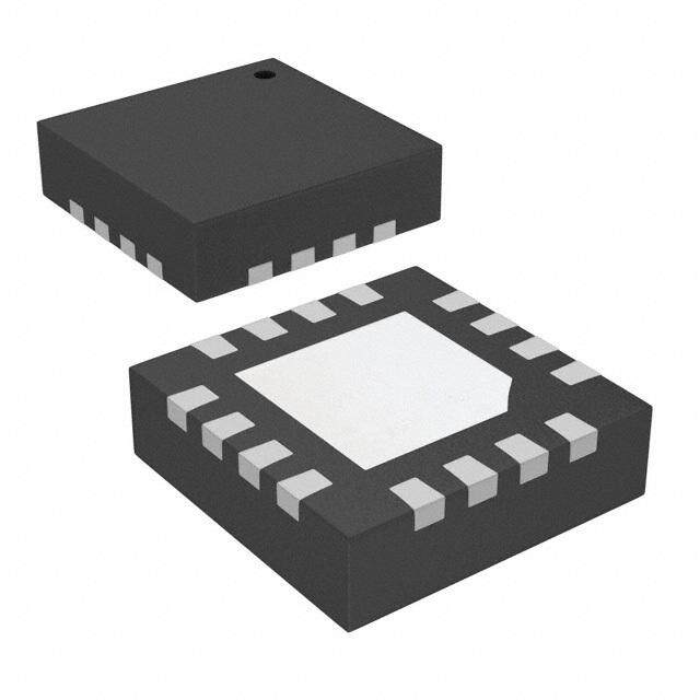
| 供应商器件封装 | 10-WSON (3x3) |
| 其它名称 | 296-35633-1 |
| 包装 | 剪切带 (CT) |
| 商标 | Texas Instruments |
| 安装类型 | 表面贴装 |
| 安装风格 | SMD/SMT |
| 封装 | Reel |
| 封装/外壳 | 10-WFDFN 裸露焊盘 |
| 封装/箱体 | WSON-10 |
| 工作温度 | -40°C ~ 125°C |
| 工作温度范围 | - 40 C to + 125 C |
| 工厂包装数量 | 1000 |
| 应用 | 控制器,4 位或 6 位 VID |
| 标准包装 | 1 |
| 电压-输入 | 2.97 V ~ 5.5 V |
| 电压-输出 | 可调 |
| 电源电压 | 2.97 V to 5.5 V |
| 电源电流 | 260 uA |
| 类型 | Voltage Regulator |
| 系列 | LM10011 |
| 输入电压范围 | 2.97 V to 5.5 V |
| 输入电流 | 340 uA |
| 输出数 | 1 |
| 输出电流 | 59.2 uA |


- 商务部:美国ITC正式对集成电路等产品启动337调查
- 曝三星4nm工艺存在良率问题 高通将骁龙8 Gen1或转产台积电
- 太阳诱电将投资9.5亿元在常州建新厂生产MLCC 预计2023年完工
- 英特尔发布欧洲新工厂建设计划 深化IDM 2.0 战略
- 台积电先进制程称霸业界 有大客户加持明年业绩稳了
- 达到5530亿美元!SIA预计今年全球半导体销售额将创下新高
- 英特尔拟将自动驾驶子公司Mobileye上市 估值或超500亿美元
- 三星加码芯片和SET,合并消费电子和移动部门,撤换高东真等 CEO
- 三星电子宣布重大人事变动 还合并消费电子和移动部门
- 海关总署:前11个月进口集成电路产品价值2.52万亿元 增长14.8%


PDF Datasheet 数据手册内容提取
Product Sample & Technical Tools & Support & Folder Buy Documents Software Community LM10011 SNVS822A–DECEMBER2012–REVISEDNOVEMBER2014 LM10011 6/4-Bit VID Programmable Current DAC for Point of Load Regulators with Adjustable Start-Up Current 1 Features 3 Description • 1.0%OutputCurrentAccuracy(0°Cto100°C) The LM10011 is a precision, digitally programmable 1 device used to control the output voltage of a DC/DC • 1.25%OutputCurrentAccuracy(–40°Cto125°C) converter. The LM10011 outputs a dc current • InputVoltageRange:2.97Vto5.5V proportional to a 6-bit or 4-bit input word. By • PinSelectableVIDFormat(6-or4-bit) connecting the IDAC_OUT pin to the feedback node of a regulator, the regulator output voltage can be • 16SelectableStart-UpCurrents adjusted to a desired range and resolution set by the • PrecisionEnabletoSupportCustomUVLO user. As the input word counts up, the output voltage • SON-103-mm× 3-mmFootprint,0.5-mmPitch is adjusted higher based on the values of the feedbackresistorsintheconverter. • FootprintCompatiblewiththeLM10010 The current from the IDAC_OUT pin on start-up is 2 Applications programmable by an external resistor to cover the range of 0 to 56.4 µA with 4 bits of resolution. The • Broadband,Networking,andWireless MODE pin allows programming of the device through Communications a 4-bit parallel VID interface or through a 6-bit • NotebookPowerSolutions interface consisting of upper and lower 3-bit VID • PortableInstruments codes. The LM10011 is specifically designed to program a wide variety of Texas Instruments DC/DC • Battery-PoweredEquipment converters for VID (Voltage Identification) • PoweringDigitalLoadswitha6-bitor4-bit,4-Pin applications. VIDInterface DeviceInformation(1) PARTNUMBER PACKAGE BODYSIZE(NOM) LM10011 WSON(10) 3.00mm×3.00mm (1) For all available packages, see the orderable addendum at theendofthedatasheet. TypicalApplicationCircuit V V IN VIN SW OUT 2.97V to 5.5V DC/DC R FB1 FB GND R FB2 3 5 VDD 2 0 - 59.2 µA VCORE MODE IDAC_OUT 4 LM10011 10 EN VIDS 9 6 VIDC VID SET VIDB 8 Interface 7 VIDA R GND SET 1 SON-10 3 mm x 3 mm 1 An IMPORTANT NOTICE at the end of this data sheet addresses availability, warranty, changes, use in safety-critical applications, intellectualpropertymattersandotherimportantdisclaimers.PRODUCTIONDATA.
LM10011 SNVS822A–DECEMBER2012–REVISEDNOVEMBER2014 www.ti.com Table of Contents 1 Features.................................................................. 1 7.3 FeatureDescription.................................................10 2 Applications........................................................... 1 7.4 DeviceFunctionalModes........................................11 3 Description............................................................. 1 7.5 Programming...........................................................11 4 RevisionHistory..................................................... 2 8 ApplicationandImplementation........................ 13 8.1 ApplicationInformation............................................13 5 PinConfigurationandFunctions......................... 3 8.2 TypicalApplication .................................................13 6 Specifications......................................................... 3 9 PowerSupplyRecommendations...................... 16 6.1 AbsoluteMaximumRatings......................................3 10 Layout................................................................... 16 6.2 HandlingRatings.......................................................4 6.3 RecommendedOperatingConditions.......................4 10.1 LayoutGuidelines.................................................16 6.4 ThermalInformation..................................................4 10.2 LayoutExample....................................................17 6.5 ElectricalCharacteristics...........................................5 11 DeviceandDocumentationSupport................. 18 6.6 TypicalCharacteristics..............................................7 11.1 Trademarks...........................................................18 7 DetailedDescription.............................................. 9 11.2 ElectrostaticDischargeCaution............................18 7.1 Overview...................................................................9 11.3 Glossary................................................................18 7.2 FunctionalBlockDiagram.........................................9 12 Mechanical,Packaging,andOrderable Information........................................................... 18 4 Revision History ChangesfromOriginal(December2012)toRevisionA Page • AddedPinConfigurationandFunctionssection,HandlingRatingtable,FeatureDescriptionsection,Device FunctionalModes,ApplicationandImplementationsection,PowerSupplyRecommendationssection,Layout section,DeviceandDocumentationSupportsection,andMechanical,Packaging,andOrderableInformation section ................................................................................................................................................................................... 1 2 SubmitDocumentationFeedback Copyright©2012–2014,TexasInstrumentsIncorporated ProductFolderLinks:LM10011
LM10011 www.ti.com SNVS822A–DECEMBER2012–REVISEDNOVEMBER2014 5 Pin Configuration and Functions 10-PIN WSONPACKAGE TOPVIEW GND 1 10 VIDS IDAC_OUT 2 9 VIDC VDD 3 DAP 8 VIDB EN 4 7 VIDA MODE 5 6 SET PinFunctions PIN I/O DESCRIPTION NAME NUMBER GND 1 – Ground IDAC_OUT 2 O OutputpinofthecurrentDACthatconnectstothefeedbacknodeoftheregulator. Positivesupplyinput.Operatingvoltageis2.97Vto5.5V.Itisrecommendedtoaddasmall VDD 3 I 1-nForgreaterbypasscapacitorfromthispintoGND. EN 4 I Precisionenableinput.TheLM10011willoperatewhentheENpinvoltageexceeds1.34V. MODEwillsettheVIDoperatingmode.ConnectingMODEtoVDDwillselecta4-bitparallel MODE 5 – interface.ConnectingMODEtoGNDwillselecta4-pin,6-bitinterface. AresistorconnectedfromSETtoGNDwillsetthestart-upcode(current)attheIDAC_OUT SET 6 – pin.Thereare16differentstart-upcodestoselectfrom. VIDdigitalinput.In6-bitmode:Bit0whenVIDStransitionslow;Bit3whenVIDStransitions VIDA 7 I high.In4-bitmode:Bit0. VIDdigitalinput.In6-bitmode:Bit1whenVIDStransitionslow;Bit4whenVIDStransitions VIDB 8 I high.In4-bitmode:Bit1. VIDdigitalinput.In6-bitmode:Bit2whenVIDStransitionslow;Bit5whenVIDStransitions VIDC 9 I high.In4-bitmode:Bit2. VIDselectline.In6-bitmode:transitionlowselectslower3bits,transitionhighselectsupper VIDS 10 I 3bitsandupdatestheIDAC_OUTcurrenttoreflectthepresentVIDcode.In4-bitmode:Bit 3. DieAttachPad.Notelectricallyconnectedtodevice,connecttosystemgroundplanefor DAP DAP – reducedthermalresistance. 6 Specifications 6.1 Absolute Maximum Ratings(1)(2) overoperatingfree-airtemperaturerange(unlessotherwisenoted) MIN MAX UNIT VDD,EN,IDAC_OUT,MODE –0.3 6 V VIDA,VIDB,VIDC,VIDS –0.3 6 V JunctionTemperature 150 °C (1) AbsoluteMaximumRatingsindicatelimitsbeyondwhichdamagetothedevicemayoccur. (2) IfMilitary-orAerospace-specifieddevicesarerequired,pleasecontacttheTexasInstrumentsSalesOffice/Distributorsforavailability andspecifications. Copyright©2012–2014,TexasInstrumentsIncorporated SubmitDocumentationFeedback 3 ProductFolderLinks:LM10011
LM10011 SNVS822A–DECEMBER2012–REVISEDNOVEMBER2014 www.ti.com 6.2 Handling Ratings MIN MAX UNIT T Storagetemperaturerange –65 150 °C stg Humanbodymodel(HBM),perANSI/ESDA/JEDECJS-001, 2 allpins(1) V Electrostaticdischarge kV (ESD) Chargeddevicemodel(CDM),perJEDECspecification 1 JESD22-C101,allpins(2) (1) JEDECdocumentJEP155statesthat500-VHBMallowssafemanufacturingwithastandardESDcontrolprocess. (2) JEDECdocumentJEP157statesthat250-VCDMallowssafemanufacturingwithastandardESDcontrolprocess. 6.3 Recommended Operating Conditions overoperatingfree-airtemperaturerange(unlessotherwisenoted) MIN MAX UNIT VDD 2.97 5.5 V IDAC_OUT –0.3 VDD–1.75 V VIDA,VIDB,VIDC,VIDS,EN,MODE –0.3 5.5 V JunctionTemperature −40 125 °C AmbientTemperature −40 125 °C 6.4 Thermal Information LM10011 THERMALMETRIC(1) DSC UNIT 10PINS R Junction-to-ambientthermalresistance(2) 52.1 θJA R Junction-to-case(top)thermalresistance(3) 30.6 θJC(top) R Junction-to-boardthermalresistance(4) 26.8 θJB °C/W ψ Junction-to-topcharacterizationparameter(5) 0.9 JT ψ Junction-to-boardcharacterizationparameter(6) 26.9 JB R Junction-to-case(bottom)thermalresistance(7) 7.7 θJC(bot) (1) Formoreinformationabouttraditionalandnewthermalmetrics,seetheICPackageThermalMetricsapplicationreport,SPRA953. (2) Thejunction-to-ambientthermalresistanceundernaturalconvectionisobtainedinasimulationonaJEDEC-standard,high-Kboard,as specifiedinJESD51-7,inanenvironmentdescribedinJESD51-2a. (3) Thejunction-to-case(top)thermalresistanceisobtainedbysimulatingacoldplatetestonthepackagetop.NospecificJEDEC- standardtestexists,butaclosedescriptioncanbefoundintheANSISEMIstandardG30-88. (4) Thejunction-to-boardthermalresistanceisobtainedbysimulatinginanenvironmentwitharingcoldplatefixturetocontrolthePCB temperature,asdescribedinJESD51-8. (5) Thejunction-to-topcharacterizationparameter,ψ ,estimatesthejunctiontemperatureofadeviceinarealsystemandisextracted JT fromthesimulationdataforobtainingR ,usingaproceduredescribedinJESD51-2a(sections6and7). θJA (6) Thejunction-to-boardcharacterizationparameter,ψ ,estimatesthejunctiontemperatureofadeviceinarealsystemandisextracted JB fromthesimulationdataforobtainingR ,usingaproceduredescribedinJESD51-2a(sections6and7). θJA (7) Thejunction-to-case(bottom)thermalresistanceisobtainedbysimulatingacoldplatetestontheexposed(power)pad.Nospecific JEDECstandardtestexists,butaclosedescriptioncanbefoundintheANSISEMIstandardG30-88. Spacer 4 SubmitDocumentationFeedback Copyright©2012–2014,TexasInstrumentsIncorporated ProductFolderLinks:LM10011
LM10011 www.ti.com SNVS822A–DECEMBER2012–REVISEDNOVEMBER2014 6.5 Electrical Characteristics TypicalvaluescorrespondtoT =25°C.Minimumandmaximumlimitsapplyover–40°Cto125°Cjunctiontemperaturerange J unlessotherwisestated.(1)(2) PARAMETER TESTCONDITIONS MIN TYP MAX UNIT SUPPLY,UVLO,ANDENABLE IQ Quiescentcurrent VDD=5.0V,VEN=2.0V 260 300 µA IQ_FS Quiescentcurrent,IDAC_OUT=IFS_6 VDD=5.0V,VEN=2.0V,IFS_6 382 µA IQ_DIS Quiescentcurrentdisabled VDD=5.0V,VEN=0.0V 45 65 µA VUVLO_R Undervoltagerisingthreshold VDDrising 2.65 2.95 V VUVLO_F Undervoltagefallingthreshold VDDfalling 2.2 2.45 V VUVLO_HYS Hysteresis 200 mV VEN Enablerisingthreshold VENrising 1.20 1.34 1.45 V VEN_HYS Enablehysteresis 50 100 180 mV IEN Enablepullupcurrent 2 µA IDAC_OUT ACC Accuracy Measuredatfullscale –1.25 1.25 % ACC Accuracy Measuredatfullscale,0°Cto100°C –1.0 1.0 % LSB_6 DACstepsize,6-bitmode IFS_6/(26–1) 940 nA LSB_4 DACstepsize,4-bitmode IFS_4/(24–1) 3.76 µA IFS_6 Full-scaleoutputcurrent(6-bitmode) VID[5:0]=000000b 59.2 µA IFS_4 Full-scaleoutputcurrent(4-bitmode) VID[3:0]=0000b 56.4 µA INL Integralnon-linearity –1 1 LSB_6 DNL Differentialnon-linearity –0.25 0.25 LSB_6 OFFSET Offsetcurrent VID[5:0]=111111b(6-bit),VID[3:0]=1111b(4-bit) 60 nA VOUT_MAX IDAC_OUTcompliancevoltage VDD=3V,VDD-VIDAC_OUT 1.75 V START-UPSETCURRENT VSETFSR SETpinvoltageFSR 1.12 1.2 1.23 V SETRES SETADCresolution 4 bits SETRNG SETADCcurrentfull-scalerange 56.4 µA ISET SETCurrent 4.75 5.1 5.40 µA SET0 Start-upDACerror,code0 RSET=0Ω,IDAC_OUT=56.4µA 0 0 LSB SET1 Start-upDACerror,code1 RSET=21.0kΩ(3),IDAC_OUT=52.7µA 0 0 LSB SET2 Start-upDACerror,code2 RSET=35.7kΩ(3),IDAC_OUT=48.9µA 0 0 LSB SET3 Start-upDACerror,code3 RSET=51.1kΩ(3),IDAC_OUT=45.2µA 0 0 LSB SET4 Start-upDACerror,code4(4) RSET=71.5kΩ(3),IDAC_OUT=41.4µA 0 1 LSB SET5 Start-upDACerror,code5(4) RSET=86.6kΩ(3),IDAC_OUT=37.7µA 0 1 LSB SET6 Start-upDACerror,code6(4) RSET=105kΩ(3),IDAC_OUT=33.9µA 0 1 LSB SET7 Start-upDACerror,code7(4) RSET=118kΩ(3),IDAC_OUT=30.1µA 0 1 LSB SET8 Start-upDACerror,code8(4) RSET=140kΩ(3),IDAC_OUT=26.4µA 0 1 LSB SET9 Start-upDACerror,code9(4) RSET=154kΩ(3),IDAC_OUT=22.6µA 0 1 LSB SET10 Start-upDACerror,code10(4) RSET=169kΩ(3),IDAC_OUT=18.8µA 0 1 LSB SET11 Start-upDACerror,code11(4) RSET=182kΩ(3),IDAC_OUT=15.1µA 0 1 LSB SET12 Start-upDACerror,code12(4) RSET=200kΩ(3),IDAC_OUT=11.3µA 0 1 LSB SET13 Start-upDACerror,code13(4) RSET=215kΩ(3),IDAC_OUT=7.59µA 0 1 LSB SET14 Start-upDACerror,code14(4) RSET=237kΩ(3),IDAC_OUT=3.80µA 0 1 LSB SET15 Start-upDACerror,code15 RSET=301kΩ(3),IDAC_OUT=0.06µA 0 0 LSB (1) Allhotandcoldlimitsarespecifiedbycorrelatingtheelectricalcharacteristicstoprocessandtemperaturevariationsandapplying statisticalprocesscontrol. (2) Thejunctiontemperature(T in°C)iscalculatedfromtheambienttemperature(T in°C)andpowerdissipation(P inWatts)asfollows: J A D T =T +(P ×R )whereR (in°C/W)isthepackagethermalimpedanceprovidedintheThermalInformationsection. J A D θJA θJA (3) R isbasedon1%E96standardresistorvalues. SET (4) "+1"LSBimpliesapositivestepinCODE.LSBisinreferencetoLSB_4. Copyright©2012–2014,TexasInstrumentsIncorporated SubmitDocumentationFeedback 5 ProductFolderLinks:LM10011
LM10011 SNVS822A–DECEMBER2012–REVISEDNOVEMBER2014 www.ti.com Electrical Characteristics (continued) TypicalvaluescorrespondtoT =25°C.Minimumandmaximumlimitsapplyover–40°Cto125°Cjunctiontemperaturerange J unlessotherwisestated.(1)(2) PARAMETER TESTCONDITIONS MIN TYP MAX UNIT VIDLOGICINPUTS(5) VIL Inputvoltagelow 0.75 V VIH Inputvoltagehigh 1.0 V IIL Inputcurrentlow –3.5 µA IIH Inputcurrenthigh 5 µA tDEGLITCH Inputdeglitchtime 3.6 µs t1 Inputdelaytime VIDSrisingedge 1 µs t2 InputholdtimeVIDA,VIDB,VIDCvalid VIDSfallingedge 20 µs t3 Inputdelaytime VIDSfallingedge 1 µs t4 InputholdtimeVIDA,VIDB,VIDCvalid VIDSrisingedge 20 µs t5 DelaytobeginningofIDAC_OUTtransition MeasuredfromVIDSrisingedge 6.3 10 µs t6 IDAC_OUTtransitiontime Timeconstantforexponentialrise 40 µs t7 Minimumholdtimein4-bitmode VIDA,VIDB,VIDC,VIDS 4.4 µs (5) ForVIDtiming,seeFigure1. 6 BIT MODE TIMING IDAC_OUT Update IDAC_OUT Update t6 t6 IDAC_OUT Current t5 t5 VID[5:3] Capture VID[2:0] Capture VID[5:3] Capture t2 t4 t3 VIDS t1 t1 VIDA,B,C 4 BIT MODE TIMING t6 t5 IDAC_OUT Current VID[0:3] Hold-Time t t VIDA,B,C,S DEGLITCH 7 Figure1. TimingDiagramforLM10011Communications 6 SubmitDocumentationFeedback Copyright©2012–2014,TexasInstrumentsIncorporated ProductFolderLinks:LM10011
LM10011 www.ti.com SNVS822A–DECEMBER2012–REVISEDNOVEMBER2014 6.6 Typical Characteristics Unlessotherwisespecified,thefollowingconditionsapply:T =25°C,VDD=5V.Allgraphsshowjunctiontemperature. J 390 60 VDD = 5.0V VDD = 5.0V 385 50 A) A) µ 380 n 40 T ( T ( N N E E R 375 R 30 R R U U VDD = 2.97V C C D 370 D 20 D D V VDD = 2.97V V 365 10 360 0 -50 -25 0 25 50 75 100 125 150 -50 -25 0 25 50 75 100 125 150 -81&7,21(cid:3)7(03(5$785((cid:3)(cid:11)Û&(cid:12) -81&7,21(cid:3)7(03(5$785((cid:3)(cid:11)Û&(cid:12) C010 C003 Figure2.SupplyCurrent Figure3.SupplyCurrent(ENLOW) MaximumOutputCurrentVID=[000000] 1.6 0.5 V) 1.5 0.3 E ( VDD = 5.5V AG 1.4 %) LT R ( 0.1 O O E V 1.3 RR NC VDD = 3.3V N E-0.1 PLIA 1.2 GAI M O -0.3 C 1.1 1 -0.5 -50 -25 0 25 50 75 100 125 150 -50 -25 0 25 50 75 100 125 150 -81&7,21(cid:3)7(03(5$785((cid:3)(cid:11)Û&(cid:12) -81&7,21(cid:3)7(03(5$785((cid:3)(cid:11)Û&(cid:12) C007 C005 Figure4.OutputCompliancetoPositiveRail Figure5.GainError (VDD-V ) IDAC_OUT 100 2.75 90 2.7 T (nA) 80 GE (V) 2.65 VDD RISING N 70 A RE LT 2.6 UR 60 VO C O 2.55 ET 50 VL VDD FALLING S U F D 2.5 OF 40 VD 30 2.45 20 2.4 -50 -25 0 25 50 75 100 125 150 -50 -25 0 25 50 75 100 125 150 -81&7,21(cid:3)7(03(5$785((cid:3)(cid:11)Û&(cid:12) -81&7,21(cid:3)7(03(5$785((cid:3)(cid:11)Û&(cid:12) C006 C009 Figure6.IDAC_OUTOffsetCurrent Figure7.UVLOThresholds VID=[111111] Copyright©2012–2014,TexasInstrumentsIncorporated SubmitDocumentationFeedback 7 ProductFolderLinks:LM10011
LM10011 SNVS822A–DECEMBER2012–REVISEDNOVEMBER2014 www.ti.com Typical Characteristics (continued) Unlessotherwisespecified,thefollowingconditionsapply:T =25°C,VDD=5V.Allgraphsshowjunctiontemperature. J 1.45 0.15 B) 0.1 (cid:20)(cid:21)(cid:24)Û& 1.4 S L RISING Y ( 0.05 (cid:21)(cid:24)Û& V) 1.35 RIT GE ( NEA 0 OLTA 1.3 FALLING ON-LI -0.05 EN V 1.25 AL N -0.1 R -0.15 G 1.2 E NT -0.2 -(cid:23)(cid:19)Û& I 1.15 -0.25 -50 -25 0 25 50 75 100 125 150 0 10 20 30 40 50 60 70 -81&7,21(cid:3)7(03(5$785((cid:3)(cid:11)Û&(cid:12) CODE C008 C002 Figure8.Enable(EN)Threshold Figure9.IntegralNon-Linearity 0.08 SB) -(cid:23)(cid:19)Û& (cid:21)(cid:24)Û& (cid:20)(cid:21)(cid:24)Û& L Y ( 0.06 T RI A 0.04 E N LI N- 0.02 O N L A 0 TI N E ER -0.02 F F DI -0.04 0 10 20 30 40 50 60 70 CODE C001 Figure10.DifferentialNon-Linearity 8 SubmitDocumentationFeedback Copyright©2012–2014,TexasInstrumentsIncorporated ProductFolderLinks:LM10011
LM10011 www.ti.com SNVS822A–DECEMBER2012–REVISEDNOVEMBER2014 7 Detailed Description 7.1 Overview The LM10011 is a precision current DAC used for controlling any point of load regulator with an adjustable resistorfeedbacknetwork.FourVIDcommunicationlines(VIDA,VIDB,VIDC,andVIDS)areusedtowritea6-bit or 4-bit VID value. The output of the IDAC (IDAC_OUT) is used to inject a precision current into the feedback node of a regulator, thus adjusting the output voltage. With this method, it is possible to precisely control the outputvoltageoftheregulator. An enable pin (EN) is provided to allow for a reduced quiescent current when not in use. Also, the VDD line is monitoredsothatanundervoltageeventwillshutdowntheLM10011(IDAC_OUT=0.0 µA). The device is available in a 10-pad No-Pullback Package (SON-10). The LM10011 can be used in numerous applicationswithregulatorsfrom2.97-Vto5.5-Vsupplies. 7.2 Functional Block Diagram Edge-Detector 3 µs Update DAC VIDS ReLcoegiivcer de6g µlitsch rfaislle deglitch 3 µs deglitch VID[5] D Q Logic 3 µs rise RQ VIDC Receiver deglitch UVLO VID[2] D Q fall RQ UVLO VID[4] D Q Logic 3 µs rise RQ VIDB Receiver deglitch UVLO VID[1] D Q fall RQ UVLO VID[3] D Q Logic 3 µs rise RQ VIDA Receiver deglitch UVLO VID[0] 6-BIT D Q MODE=0 DEedtegfcaetl-olr UVRLOQ MO4-DBEIT= 1 I6D AbiCt SLilmewit 0 ±( I45D-6bA.i4Ct /_/ 6O5-9Ub.2iTt )µA VID[3] VID[2] VID[1] VID Start- Up Current VID[0] Set RSET MODE UVLO VDD (VDD > 2.65V) DISABLE IREF PRECISION EN ENABLE Bandgap + (1.34V) Core - GND Copyright©2012–2014,TexasInstrumentsIncorporated SubmitDocumentationFeedback 9 ProductFolderLinks:LM10011
LM10011 SNVS822A–DECEMBER2012–REVISEDNOVEMBER2014 www.ti.com 7.3 Feature Description The LM10011 can be treated as a D/A converter, converting digital VID codes to analog outputs. The LM10011 DAC analog output is a current that flows out of the IDAC_OUT pin. The IDAC_OUT pin is intended to be connected to the feedback node of a voltage regulator as shown in Figure 11. In a typical voltage regulator, the current in R is constant by virtue of the regulator feedback loop maintaining the reference voltage at the FB2 feedback node. The current flowing through R is the same current flowing through R . When current is FB2 FB1 injected into the feedback node by the LM10011, less current is required from the R resistor. The FB1 consequence of this is that the output voltage of the regulator will decrease to maintain the total amount of currentinR toregulateatthecorrectfeedback(reference)voltage. FB2 Each VID code corresponds to a different IDAC_OUT current and thus a different output voltage. Increasing the VID code lowers the IDAC_OUT current and raises the output voltage. Decreasing the VID code raises the IDAC_OUT current and lowers the output voltage. All VID codes are decoded into a 6-bit or 4-bit current DAC outputwhethertheMODEequals0(connectedtoGND)or1(connectedtoVDD),respectively. Slave Regulator VOUT FB + + RFB1 IRFB1 VRFB1 LM10011 - + IDAC_OUT - VOUT LM10011 + RFB2 - IRFB2 VFB VID - IDAC_OUT Figure11. OutputVoltage(V )isControlledViaCurrentInjectionintotheFeedbackNode OUT 7.3.1 CurrentDAC The LM10011 current DAC is based on a low-voltage bandgap reference setting a current through a precision adjustable resistor. This bandgap is trimmed for precision and gives excellent performance over temperature. The output current has a maximum full-scale range [VID = 000000b] of 59.2 µA and is adjustable with a 6- or 4- bit VID word. This allows for 64 or 16 settings with a resolution of 940 nA or 3.76 µA, respectively. The current DAC also has a slew limit to prevent abrupt changes in the output. The slew limit is represented as a time constant, t = 40 µs, in the Electrical Characteristics table. A deglitch filter for the VID inputs provides noise 6 immunityandeffectivelyaddsasmalldelayfromthetransitionofaVIDlinetothechangeinIDAC_OUTcurrent. 7.3.2 EnablePinandUVLO The enable (EN) pin allows the output of the device to be enabled or disabled (IDAC_OUT = 0.0 µA) with an external control signal. This pin is a precision analog input that enables the device when the voltage exceeds 1.34 V. The EN pin has 100 mV of hysteresis and will disable the output when the enable voltage falls below 1.23V.IfENisnotused,itcanbeleftopen,andwillbepulledhighbyaninternal2-μAcurrentsource.Sincethe ENpinhasapreciseturn-onthresholditcanbeusedalongwithanexternalresistordividernetworkfromVDDto configurethedevicetoturnonatapreciseinputvoltage. The LM10011 has a built-in undervoltage lockout (UVLO) protection circuit that keeps the device from operating until the input voltage reaches 2.65 V (typical). The UVLO threshold has 200 mV of hysteresis that keeps the LM10011 from responding to power-on glitches during start-up. Note that descending below the EN voltage and/ortheUVLOvoltagearefunctionallythesameasareset.Bringingthedevicebackfromalowenablesetting orfromaVDDUVLOeventwillresettheIDAC_OUTcurrenttoitsstart-upR setting. SET 10 SubmitDocumentationFeedback Copyright©2012–2014,TexasInstrumentsIncorporated ProductFolderLinks:LM10011
LM10011 www.ti.com SNVS822A–DECEMBER2012–REVISEDNOVEMBER2014 7.4 Device Functional Modes Table1liststhefunctionalmodesoftheLM10011device. Table1.ModePinSummary MODEPINCONNECTION LOGICSTATE DESCRIPTION GND 0 6-bitmode VDD 1 4-bitmode 7.5 Programming 7.5.1 VIDProgramming,6-BitMode Four pins are used to communicate with the LM10011. In 6-bit mode (MODE = 0), VIDA, VIDB, and VIDC are data lines, while VIDS is a latching strobe that programs in the LM10011 data. As shown in the 6-bit mode timing diagram of Figure 1, the falling edge of VIDS latches in the data from VIDA, VIDB, and VIDC as the lower three LSB of the IDAC_OUT value, [2:0]. After a minimum hold time (t ), the rising edge of VIDS latches in the data 2 from VIDA, VIDB, and VIDC as the upper three LSB of the IDAC_OUT value, [5:3]. Internally, a delay (t ,t ) on 3 1 VIDSallowsforthesettingofallVIDA,VIDB,andVIDClinestochangesimultaneouslyasVIDSrisesorfalls. 7.5.2 VIDProgramming,4-BitMode The LM10011 includes a 4-bit mode to facilitate parallel VID communication. In 4-bit mode (MODE = 1), VIDC, VIDB, VIDA, and VIDS are all parallel data lines. As shown in the 4-bit mode timing diagram in Figure 1, a changing edge of any of the VID communication lines will change the IDAC_OUT current to the corresponding new 4-bit value found on the data lines. There is a 3-μs deglitch filter to eliminate spurious noise events. The data must overcome the deglitch time and the minimum hold time (t ) or else the IDAC_OUT pin current may not 7 reflectthevalueindicatedattheVIDdatainputs.Duringtheholdtime,nootherdatalinecanbetransitioned. As mentioned in a previous section, for both the 4-bit and 6-bit mode, the VID data word is set so that the lowest output current is seen at the highest VID data word (59.2 µA at a code of 0d in 6-bit mode and 56.4 µA in 4-bit mode). Conversely, the lowest current is seen at the highest VID data word (0.06 µA at 63d or 15d). During VID operation with the regulator, this will translate to the lowest output voltage with the lowest VID word, 0d, and the highest output voltage with the highest VID word, 63d or 15d. The communications pins can be used with a low- voltagemicrocontrollerwithamaximumV of0.75VandaminimumV of1.0V. IL IH 7.5.3 ProgrammingtheStart-UpCurrent Depending on the value of R during start-up (when VDD > VUVLO_R and EN > VEN), the output current on SET the IDAC_OUT pin will take on 1 of 16 discrete values corresponding to the currents available in the 4-bit mode. These discrete start-up currents can be programmed by connecting a resistor (R ) from the SET pin to GND. If SET theENvoltageistoggledoraUVLOistriggeredduringoperation,thecurrentwilldefaultbacktothevaluesetby the R resistor. It takes only one VID command transition in either 4-bit or 6-bit mode to change the current to SET something other than the pre-programmed start-up current. The required R resistors and their corresponding SET start-upcurrentscodescanbefoundinTable2. Table2.Start-Up–4-BitModeCurrentswithCorrespondingR ValuesandOutputCurrents SET VIDCODE NOMINALIDAC_OUTCURRENT(µA) R (kΩ) SET 0000b(0d) 56.4 0 0001b(1d) 52.7 21.0 0010b(2d) 48.9 35.7 0011b(3d) 45.2 51.1 0100b(4d) 41.4 71.5 0101b(5d) 37.7 86.6 0110b(6d) 33.9 105 0111b(7d) 30.1 118 1000b(8d) 26.4 140 1001b(9d) 22.6 154 Copyright©2012–2014,TexasInstrumentsIncorporated SubmitDocumentationFeedback 11 ProductFolderLinks:LM10011
LM10011 SNVS822A–DECEMBER2012–REVISEDNOVEMBER2014 www.ti.com Programming (continued) Table2.Start-Up–4-BitModeCurrentswithCorrespondingR ValuesandOutputCurrents(continued) SET VIDCODE NOMINALIDAC_OUTCURRENT(µA) R (kΩ) SET 1010b(10d) 18.8 169 1011b(11d) 15.1 182 1100b(12d) 11.3 200 1101b(13d) 7.59 215 1110b(14d) 3.80 237 1111b(15d) 0.06 301 Codes 0100b (4d) through 1110b (14d) will start-up into either the selected code or 1 code higher. This means thattheoutputvoltageofthePOLmaystart-upintotheselectedoutputvoltageor1LSBhigher. 7.5.4 IDAC_OUTCurrentValues Table3.IDAC_OUTCurrentsandCorresponding Table3.IDAC_OUTCurrentsandCorresponding VIDCodes(continued) VIDCodes VIDCODE(6-BIT[4-BIT]) IDACCURRENT(µA) VIDCODE(6-BIT[4-BIT]) IDACCURRENT(µA) 32d 29.2 0d 59.2 33d 28.2 1d 58.3 34d 27.3 2d 57.4 35d[8d] 26.4 3d[0d] 56.4 36d 25.4 4d 55.5 37d 24.5 5d 54.6 38d 23.6 6d 53.6 39d[9d] 22.6 7d[1d] 52.7 40d 21.6 8d 51.7 41d 20.7 9d 50.8 42d 19.8 10d 49.8 43d[10d] 18.8 11d[2d] 48.9 44d 17.9 12d 48.0 45d 17.0 13d 47.0 46d 16.0 14d 46.1 47d[11d] 15.1 15d[3d] 45.2 48d 14.1 16d 44.2 49d 13.2 17d 43.3 50d 12.3 18d 42.3 51d[12d] 11.3 19d[4d] 41.4 52d 10.4 20d 40.5 53d 9.50 21d 39.5 54d 8.52 22d 38.6 55d[13d] 7.59 23d[5d] 37.7 56d 6.60 24d 36.7 57d 5.70 25d 35.7 58d 4.74 26d 34.8 59d[14d] 3.80 27d[6d] 33.9 60d 2.87 28d 33.0 61d 1.93 29d 32.0 62d 1.00 30d 31.1 63d[15d] 0.06 31d[7d] 30.1 12 SubmitDocumentationFeedback Copyright©2012–2014,TexasInstrumentsIncorporated ProductFolderLinks:LM10011
LM10011 www.ti.com SNVS822A–DECEMBER2012–REVISEDNOVEMBER2014 8 Application and Implementation NOTE Information in the following applications sections is not part of the TI component specification, and TI does not warrant its accuracy or completeness. TI’s customers are responsible for determining suitability of components for their purposes. Customers should validateandtesttheirdesignimplementationtoconfirmsystemfunctionality. 8.1 Application Information LM10011 is a precision, digitally programmable device used for controlling the dc-dc converter output voltage. The LM10011 GUI design tool is available at www.ti.com/product/LM10011 and can be used to program any voltage regulator output to a desired range and resolution. The GUI enables changing the output voltage of the on-board POL based on direct user input. It is also able to assist the power designer in selecting the correct externalcomponentsneededforanygivenapplication. 8.2 Typical Application In this example, an LM21215A-1 is used as the voltage regulator and the desired range of output voltage operation is 0.7 V to 1.1 V. The LM10011 can provide control of the output voltage within this range with 6 bits or 4 bits of resolution. For this example, the 400 mV of voltage range translates to a V of 400 mV / 63 = 6.4 OUT_LSB mV (26.7 mV in 4-bit mode) at the regulator output. In this calculation, 1% resistor values are used. A schematic forthisexampleisshowninFigure12. TSSOP-20 L F VIN 5,6,7 PVIN SW 11-16 VOUT 3V to 5.5V CIN RF 3 EN COUT 0.7V to 1.1V C 4 C3 AVIN R CF LM21215A-1 19 FB1 RC2 FB CC1 RC1 optional 2 SS/ COMP 18 RFB2 TRK C SS C C2 1 17 SYNC PGOOD PGND AGND 8,9,10 20 3 CBYPASS 0 - 59.2 µA 4 EN VDDIDAC_OUT 2 C VDD 5 DVDD18 CVDD MODE R PU1:4 10 LM10011 VIDS 9 VCNTL[3] VIDC VCNTL[2] TMS320C6670/ 6 SET VIDB 87 VCNTL[1] TMS320C6678 R VIDA VCNTL[0] SET GND 1 SON-10 3 mm x 3 mm Figure12. 6-BitModeDesignExample Copyright©2012–2014,TexasInstrumentsIncorporated SubmitDocumentationFeedback 13 ProductFolderLinks:LM10011
LM10011 SNVS822A–DECEMBER2012–REVISEDNOVEMBER2014 www.ti.com Typical Application (continued) 8.2.1 DesignRequirements Table4liststhedesignparameters. Table4.DesignParameters DESIGNPARAMETER EXAMPLEVALUE Outputvoltagerange 0.7Vto1.1V Startupvoltage 1.1V Mode 0 8.2.2 DetailedDesignProcedure 8.2.2.1 SettingtheV RangeandLSB OUT Looking at the Typical Application Circuit in Figure 12, the following equation defines V of a given regulator OUT (validforV >V ): OUT FB R VOUT = VFBx1+RFB1 - IDAC_OUT x RFB1 FB2 (1) Here, the output voltage is a function of the resistor divider from R and R . Using the LM10011, there is a FB1 FB2 current supplied by the IDAC_OUT pin that helps drive current through the feedback resistor R , thus lowering FB2 the necessary current supplied through R , and hence lowering V . To calculate the nominal (maximum) FB1 OUT V ,useanIDAC_OUTvalueof0µA. OUT The change in the output voltage can be analyzed based on the resolution of the current DAC from the LM10011 compared to the desired resolution of the output swing of the regulator. R is designed to provide the desired FB1 V withtheequation: OUT_LSB V = LSB x R OUT_LSB FB1 (2) Where LSB = LSB_6 (940 nA) from the electrical characteristics table (see Electrical Characteristics). Based on the desired nominal V (with IDAC_OUT = 0 µA) and the calculated R from Equation 2, R can be solved OUT FB1 FB2 usingEquation1. 8.2.2.2 4-BitModeDesignExample Designing with the LM10011 in 4-bit mode is similar to designing in 6-bit mode. The only differences are the LSB value(LSB=LSB_4=3.76µA)inEquation2andfull-scalecurrentrange(IDAC_OUT=56.4 µA). 8.2.2.3 SettingtheStart-UpVoltagewithR SET R is chosen depending on the required start-up voltage for the particular application. The user must use SET Equation 3 and solve for the required IDAC_OUT by inputting the known values of R and R , V , and the FB1 FB2 FB desired start-up output voltage, V . Once IDAC_OUT is solved for, choose an R based on Table 2 to select OUT SET a start-up code to yield a current closely matching the calculated result. Use the equation below to solve for the requiredIDAC_OUTvalueatstart-up. 1 R IDAC_OUT = V x 1+ FB1 - V R FB R OUT FB1 FB2 (3) 8.2.2.4 ExampleSolution Whilein6-bitmode,assuminga400-mVoutputrange,64VIDcodes,andanIDACLSBof0.940 µA,itisdesired to have a V with an LSB of 6.4 mV and a default value of 1.1 V with a 1.05-V start-up voltage using an OUT LM21215A-1regulator(V =0.6V): FB 6.4mV = 0.940µA x RFB1 (4) RFB1 = 6.8k(cid:13) (5) Using 1% standard resistor values, R can be set to 6.81 kΩ. Now calculate R based on R and the FB1 FB2 FB1 maximumV of1.1VusingEquation1. OUT 14 SubmitDocumentationFeedback Copyright©2012–2014,TexasInstrumentsIncorporated ProductFolderLinks:LM10011
LM10011 www.ti.com SNVS822A–DECEMBER2012–REVISEDNOVEMBER2014 6.81k(cid:13) 1.1V = .6Vx1+ -0V R FB2 (6) RFB2 = 8.1k(cid:13) (7) Using 1% standard resistor values, R can be set to 8.06 kΩ. This will yield a regulator output range of 0.704 V FB2 (CODE 0d) to 1.107 V (CODE 63d). Values calculated here will be dependent on the accuracy of the regulator, theLM10011IDAC_OUT,andtheresistorvaluesusedinthecircuit. Table 5 shows the codes and some of the resultant values of the IDAC current and the corresponding regulator outputvoltageforthepreviousexample. Table5.6-BitVIDCodeswithIDACCurrentandRegulatorVoltagefortheExampleinFigure12. VIDCODE IDAC_OUTCURRENT(µA) REGULATORVOLTAGE(V) 000000b(0d) 59.2 0.704 000001b(1d) 58.3 0.710 000010b(2d) 57.4 0.716 000011b(3d) 56.4 0.729 .... .... .... 111100b(60d) 2.87 1.087 111101b(61d) 1.93 1.094 111110b(62d) 1.00 1.100 111111b(63d) 0.06 1.107 The required IDAC_OUT value during start-up can be calculated based on the desired start-up voltage of 1.05 V and the R and R resistors found in the previous calculations. Using Equation 3 to solve for the required FB1 FB2 start-upIDAC_OUTcurrentresultsinastart-upcurrentof8.36 µA. 1 6.81k(cid:13) IDAC_OUT = 6.81k(cid:13) 0.6V x1+8.06k(cid:13) - 1.05V = 8.36µA (8) Choose a resistor in Table 2 that selects a start-up code that produces a current close to 8.36 µA. An R of SET 215kΩ selectsanominalstart-upcodeof13dyieldingacurrentof7.59 µAandstart-upvoltageof1.054V. NOTE UsinganR of215kΩ mayalsoselectacodeof14d(+1LSB)yieldingacurrentof3.80 SET µAandastart-upvoltageof1.081V. 8.2.3 ApplicationCurves 1.14 1.11 1.08 1.05 1.02 V) 0.99 ge ( 0.96 olta 0.93 V 0.9 ut 0.87 p ut 0.84 O 0.81 0.78 0.75 VIN = 2.9V 0.72 VIN = 5.5V 0.69 0 5 10 15 20 25 30 35 40 45 50 55 60 65 6-Bit VID Code (Decimal) Figure13. OutputVoltagevs.CodeforLM21kwithLM10011 Copyright©2012–2014,TexasInstrumentsIncorporated SubmitDocumentationFeedback 15 ProductFolderLinks:LM10011
LM10011 SNVS822A–DECEMBER2012–REVISEDNOVEMBER2014 www.ti.com 9 Power Supply Recommendations The LM10011 can be driven from a PWM controller V pin or from the V supply pin as shown in Figure 12. To DD IN ensurereliableoperation,theLM10011V inputpowersupplymustbelimitedto6Vmaximum. DD 10 Layout 10.1 Layout Guidelines ThefollowingguidelinesshouldbefollowedwhendesigningthePCboardfortheLM10011: • PlacetheLM10011closetotheregulatorfeedbackpintominimizetheFBtracelength. • Place a small capacitor, C , (1 nF) directly adjacent to the VDD and GND pins of the LM10011 to help VDD minimizetransientswhichmayoccurontheinputsupplyline. • The high-current path from the board input to the load and the return path should be parallel and close to eachothertominimizeloopinductance. • The ground connections for the various components around the LM10011 should be connected directly to each other, and to the LM10011 GND pins, and then connected to the system ground at one point. Do not connectthevariouscomponentgroundstoeachotherthroughthehigh-currentgroundline. • For additional information about the operation of the regulator, please consult the respective data sheet and applicationnotesontherespectiveevaluationboards. 16 SubmitDocumentationFeedback Copyright©2012–2014,TexasInstrumentsIncorporated ProductFolderLinks:LM10011
LM10011 www.ti.com SNVS822A–DECEMBER2012–REVISEDNOVEMBER2014 10.2 Layout Example Figure14. TypicalTopLayerLayout Copyright©2012–2014,TexasInstrumentsIncorporated SubmitDocumentationFeedback 17 ProductFolderLinks:LM10011
LM10011 SNVS822A–DECEMBER2012–REVISEDNOVEMBER2014 www.ti.com 11 Device and Documentation Support 11.1 Trademarks Alltrademarksarethepropertyoftheirrespectiveowners. 11.2 Electrostatic Discharge Caution Thesedeviceshavelimitedbuilt-inESDprotection.Theleadsshouldbeshortedtogetherorthedeviceplacedinconductivefoam duringstorageorhandlingtopreventelectrostaticdamagetotheMOSgates. 11.3 Glossary SLYZ022—TIGlossary. Thisglossarylistsandexplainsterms,acronyms,anddefinitions. 12 Mechanical, Packaging, and Orderable Information The following pages include mechanical, packaging, and orderable information. This information is the most current data available for the designated devices. This data is subject to change without notice and revision of thisdocument.Forbrowser-basedversionsofthisdatasheet,refertotheleft-handnavigation. 18 SubmitDocumentationFeedback Copyright©2012–2014,TexasInstrumentsIncorporated ProductFolderLinks:LM10011
PACKAGE OPTION ADDENDUM www.ti.com 6-Feb-2020 PACKAGING INFORMATION Orderable Device Status Package Type Package Pins Package Eco Plan Lead/Ball Finish MSL Peak Temp Op Temp (°C) Device Marking Samples (1) Drawing Qty (2) (6) (3) (4/5) LM10011SD/NOPB ACTIVE WSON DSC 10 1000 Green (RoHS SN Level-1-260C-UNLIM -40 to 125 L271B & no Sb/Br) LM10011SDX/NOPB ACTIVE WSON DSC 10 4500 Green (RoHS SN Level-1-260C-UNLIM -40 to 125 L271B & no Sb/Br) (1) The marketing status values are defined as follows: ACTIVE: Product device recommended for new designs. LIFEBUY: TI has announced that the device will be discontinued, and a lifetime-buy period is in effect. NRND: Not recommended for new designs. Device is in production to support existing customers, but TI does not recommend using this part in a new design. PREVIEW: Device has been announced but is not in production. Samples may or may not be available. OBSOLETE: TI has discontinued the production of the device. (2) RoHS: TI defines "RoHS" to mean semiconductor products that are compliant with the current EU RoHS requirements for all 10 RoHS substances, including the requirement that RoHS substance do not exceed 0.1% by weight in homogeneous materials. Where designed to be soldered at high temperatures, "RoHS" products are suitable for use in specified lead-free processes. TI may reference these types of products as "Pb-Free". RoHS Exempt: TI defines "RoHS Exempt" to mean products that contain lead but are compliant with EU RoHS pursuant to a specific EU RoHS exemption. Green: TI defines "Green" to mean the content of Chlorine (Cl) and Bromine (Br) based flame retardants meet JS709B low halogen requirements of <=1000ppm threshold. Antimony trioxide based flame retardants must also meet the <=1000ppm threshold requirement. (3) MSL, Peak Temp. - The Moisture Sensitivity Level rating according to the JEDEC industry standard classifications, and peak solder temperature. (4) There may be additional marking, which relates to the logo, the lot trace code information, or the environmental category on the device. (5) Multiple Device Markings will be inside parentheses. Only one Device Marking contained in parentheses and separated by a "~" will appear on a device. If a line is indented then it is a continuation of the previous line and the two combined represent the entire Device Marking for that device. (6) Lead/Ball Finish - Orderable Devices may have multiple material finish options. Finish options are separated by a vertical ruled line. Lead/Ball Finish values may wrap to two lines if the finish value exceeds the maximum column width. Important Information and Disclaimer:The information provided on this page represents TI's knowledge and belief as of the date that it is provided. TI bases its knowledge and belief on information provided by third parties, and makes no representation or warranty as to the accuracy of such information. Efforts are underway to better integrate information from third parties. TI has taken and continues to take reasonable steps to provide representative and accurate information but may not have conducted destructive testing or chemical analysis on incoming materials and chemicals. TI and TI suppliers consider certain information to be proprietary, and thus CAS numbers and other limited information may not be available for release. In no event shall TI's liability arising out of such information exceed the total purchase price of the TI part(s) at issue in this document sold by TI to Customer on an annual basis. Addendum-Page 1
PACKAGE OPTION ADDENDUM www.ti.com 6-Feb-2020 Addendum-Page 2
PACKAGE MATERIALS INFORMATION www.ti.com 14-Nov-2014 TAPE AND REEL INFORMATION *Alldimensionsarenominal Device Package Package Pins SPQ Reel Reel A0 B0 K0 P1 W Pin1 Type Drawing Diameter Width (mm) (mm) (mm) (mm) (mm) Quadrant (mm) W1(mm) LM10011SD/NOPB WSON DSC 10 1000 178.0 12.4 3.3 3.3 1.0 8.0 12.0 Q1 LM10011SDX/NOPB WSON DSC 10 4500 330.0 12.4 3.3 3.3 1.0 8.0 12.0 Q1 PackMaterials-Page1
PACKAGE MATERIALS INFORMATION www.ti.com 14-Nov-2014 *Alldimensionsarenominal Device PackageType PackageDrawing Pins SPQ Length(mm) Width(mm) Height(mm) LM10011SD/NOPB WSON DSC 10 1000 210.0 185.0 35.0 LM10011SDX/NOPB WSON DSC 10 4500 367.0 367.0 35.0 PackMaterials-Page2
MECHANICAL DATA DSC0010A SDA10A (Rev A) www.ti.com
IMPORTANTNOTICEANDDISCLAIMER TI PROVIDES TECHNICAL AND RELIABILITY DATA (INCLUDING DATASHEETS), DESIGN RESOURCES (INCLUDING REFERENCE DESIGNS), APPLICATION OR OTHER DESIGN ADVICE, WEB TOOLS, SAFETY INFORMATION, AND OTHER RESOURCES “AS IS” AND WITH ALL FAULTS, AND DISCLAIMS ALL WARRANTIES, EXPRESS AND IMPLIED, INCLUDING WITHOUT LIMITATION ANY IMPLIED WARRANTIES OF MERCHANTABILITY, FITNESS FOR A PARTICULAR PURPOSE OR NON-INFRINGEMENT OF THIRD PARTY INTELLECTUAL PROPERTY RIGHTS. These resources are intended for skilled developers designing with TI products. You are solely responsible for (1) selecting the appropriate TI products for your application, (2) designing, validating and testing your application, and (3) ensuring your application meets applicable standards, and any other safety, security, or other requirements. These resources are subject to change without notice. TI grants you permission to use these resources only for development of an application that uses the TI products described in the resource. Other reproduction and display of these resources is prohibited. No license is granted to any other TI intellectual property right or to any third party intellectual property right. TI disclaims responsibility for, and you will fully indemnify TI and its representatives against, any claims, damages, costs, losses, and liabilities arising out of your use of these resources. TI’s products are provided subject to TI’s Terms of Sale (www.ti.com/legal/termsofsale.html) or other applicable terms available either on ti.com or provided in conjunction with such TI products. TI’s provision of these resources does not expand or otherwise alter TI’s applicable warranties or warranty disclaimers for TI products. Mailing Address: Texas Instruments, Post Office Box 655303, Dallas, Texas 75265 Copyright © 2020, Texas Instruments Incorporated