ICGOO在线商城 > 集成电路(IC) > PMIC - 稳压器 - 专用型 > NCP51199PDR2G
 Datasheet下载
- 型号: NCP51199PDR2G
- 制造商: ON Semiconductor
- 库位|库存: xxxx|xxxx
- 要求:
| 数量阶梯 | 香港交货 | 国内含税 |
| +xxxx | $xxxx | ¥xxxx |
查看当月历史价格
查看今年历史价格
NCP51199PDR2G产品简介:
ICGOO电子元器件商城为您提供NCP51199PDR2G由ON Semiconductor设计生产,在icgoo商城现货销售,并且可以通过原厂、代理商等渠道进行代购。 NCP51199PDR2G价格参考¥1.24-¥1.24。ON SemiconductorNCP51199PDR2G封装/规格:PMIC - 稳压器 - 专用型, - LDO (Linear), DDR Voltage Regulator IC 1 Output 8-SOIC。您可以下载NCP51199PDR2G参考资料、Datasheet数据手册功能说明书,资料中有NCP51199PDR2G 详细功能的应用电路图电压和使用方法及教程。
NCP51199PDR2G 是 ON Semiconductor(安森美半导体)推出的一款专用型电源管理集成电路(PMIC),属于 PMIC - 稳压器 - 专用型类别。该器件主要用于需要高效、紧凑和低功耗电源解决方案的应用场景,其典型应用场景包括:

1. 便携式电子设备
   NCP51199PDR2G 非常适合用于便携式设备,例如智能手机、平板电脑、可穿戴设备(如智能手表和健身追踪器)以及便携式医疗设备。这些设备通常对电源效率和空间要求较高,而该芯片的高效能和小尺寸特性能够满足这些需求。

2. 电池供电系统
   在电池供电的系统中,例如无线传感器节点、手持式工具或物联网(IoT)设备,NCP51199PDR2G 的低静态电流(Iq)和高效率特性有助于延长电池寿命。

3. 通信设备
   该芯片适用于各种通信设备,例如路由器、调制解调器、Wi-Fi 模块和其他网络设备。它能够为这些设备中的处理器、存储器和其他关键组件提供稳定的电源。

4. 消费类电子产品
   包括数字电视、机顶盒、音频设备等在内的消费类电子产品,可能需要多个电压轨来支持不同的功能模块。NCP51199PDR2G 可以作为整体电源管理方案的一部分,提供高效的电源转换。

5. 工业控制与自动化
   在工业环境中,NCP51199PDR2G 可以为微控制器、传感器接口、数据采集系统等提供稳定且可靠的电源支持。其抗噪能力和稳定性使其在严苛的工业条件下表现优异。

6. 汽车电子辅助系统
   虽然 NCP51199PDR2G 不是专门为汽车设计,但它也可以用于一些非核心的汽车电子应用,例如信息娱乐系统、车内照明控制或传感器模块,特别是在对功耗和空间有限制的情况下。

总之,NCP51199PDR2G 凭借其高集成度、低功耗和高效能的特点,广泛应用于需要精密电源管理的各种领域,尤其适合对体积、效率和成本敏感的设计。
| 参数 | 数值 |
| 产品目录 | 集成电路 (IC)半导体 |
| 描述 | IC CONV DDR DDR2 DDR3线性稳压器 DDR 2Amp Source Sink VTT Termination Reg |
| 产品分类 | |
| 品牌 | ON Semiconductor |
| 产品手册 | |
| 产品图片 | |
| rohs | 符合RoHS无铅 / 符合限制有害物质指令(RoHS)规范要求 |
| 产品系列 | 电源管理 IC,线性稳压器,ON Semiconductor NCP51199PDR2G- |
| 数据手册 | |
| 产品型号 | NCP51199PDR2G |
| 产品种类 | |
| 供应商器件封装 | * |
| 包装 | * |
| 商标 | ON Semiconductor |
| 安装类型 | * |
| 安装风格 | SMD/SMT |
| 封装 | Reel |
| 封装/外壳 | * |
| 封装/箱体 | SOIC-8 |
| 工作温度 | -40°C ~ 85°C |
| 工厂包装数量 | 2500 |
| 应用 | 转换器,DDR |
| 最大工作温度 | + 85 C |
| 最大输入电压 | 5.5 V |
| 最小工作温度 | - 40 C |
| 最小输入电压 | 1.2 V |
| 标准包装 | 2,500 |
| 电压-输入 | 1.5 V ~ 5.5 V |
| 电压-输出 | - |
| 系列 | NCP51199 |
| 负载调节 | +/- 10 mV |
| 输出数 | 1 |
| 输出电流 | 2 A |
| 输出端数量 | 1 |
| 输出类型 | Adjustable |


- 商务部:美国ITC正式对集成电路等产品启动337调查
- 曝三星4nm工艺存在良率问题 高通将骁龙8 Gen1或转产台积电
- 太阳诱电将投资9.5亿元在常州建新厂生产MLCC 预计2023年完工
- 英特尔发布欧洲新工厂建设计划 深化IDM 2.0 战略
- 台积电先进制程称霸业界 有大客户加持明年业绩稳了
- 达到5530亿美元!SIA预计今年全球半导体销售额将创下新高
- 英特尔拟将自动驾驶子公司Mobileye上市 估值或超500亿美元
- 三星加码芯片和SET,合并消费电子和移动部门,撤换高东真等 CEO
- 三星电子宣布重大人事变动 还合并消费电子和移动部门
- 海关总署:前11个月进口集成电路产品价值2.52万亿元 增长14.8%


PDF Datasheet 数据手册内容提取
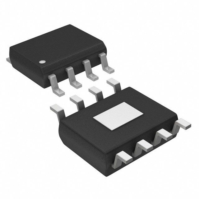
NCP51199, NCV51199 DDR 2-Amp Source / Sink V Termination Regulator TT The NCP/NCV51199 is a linear regulator designed to supply a regulated V termination voltage for DDR−2 and DDR−3 memory TT applications. The regulator is capable of actively sourcing and sinking ±2 A peak currents for DDR−2, and DDR−3 up to ±1.5 A while www.onsemi.com regulating the V output voltage to within ±10 mV. The output TT termination voltage is regulated to track V / 2 by two external MARKING DDQ voltage divider resistors connected to the PV , GND, and V pins. DIAGRAM CC REF The NCP/NCV51199 incorporates a high−speed differential 8 amplifier to provide ultra−fast response to line and load transients. SOIC8−NB EP XXXXXX Other features include source/sink current limiting, soft−start and 8 PD SUFFIX ALYW on−chip thermal shutdown protection. CASE 751BU (cid:2) 1 Features 1 • Supports DDR−2 V Termination to ±2 A, DDR−3 to ±1.5 A (peak) TT XXXXXX = Specific Device Code • Stable with 10 (cid:2)F Ceramic Capacitance on V Output A = Assembly Location TT • L = Wafer Lot Integrated Power MOSFETs Y = Year • High Accuracy VTT Output at Full−Load WW = Work Week • Fast Transient Response (cid:2) = Pb−Free Package • Built−in Soft−Start • Shutdown for Standby or Suspend Mode • PIN CONNECTION Integrated Thermal and Current−Limit Protection • NCV Prefix for Automotive and Other Applications Requiring 1 8 PVCC NC Unique Site and Control Change Requirements; AEC−Q100 GND NC Qualified and PPAP Capable • VREF VCC These Devices are Pb−Free and are RoHS Compliant VTT NC SOIC−8 EP Typical Applications • SDRAM Termination Voltage for DDR−2 / DDR−3 • Motherboard, Notebook, and VGA Card Memory Termination ORDERING INFORMATION • Set Top Box, Digital TV, Printers See detailed ordering, marking and shipping information in the package dimensions section on page 6 of this data sheet. © Semiconductor Components Industries, LLC, 2017 1 Publication Order Number: April, 2017 − Rev. 3 NCP51199/D
NCP51199, NCV51199 NCP51199 PVCC = 1.5 to 5.0 V* 1 5 V PVCC VCC 6 C2 C3 R2 2 100k GND 3 VREF 4 VTT = 0.75 to 2.5 V* VTT C1 Enable R1 C4 100k R3 *For DDR2: PVCC = 1.8 V, VTT = 0.9 V DDR3: PVCC = 1.5 V, VTT = 0.75 V C1 = 1 (cid:2)F (Low ESR) C4 = 1000 (cid:2)F + 10 (cid:2)F (10 (cid:2)F ceramic) C2 = 470 (cid:2)F (Low ESR) R3 = Optional VTT discharge resistor C3 = 47 (cid:2)F N−ch MOSFET = Optional Enable / Disable Figure 1. Application Diagram PIN FUNCTION DESCRIPTION Pin No. Pin Name Description 1 PVCC Input voltage which supplies current to the output pin. CIN = 470 (cid:2)F with low ESR. 2 GND Common Ground 3 V Buffered reference voltage input equal to ½ of V and active low shutdown pin. An external resistor REF DDQ divider dividing down the PV voltage creates the regulated output voltage. Pulling the pin to ground CC (0.15 V maximum) turns the device off. 4 V Regulator output voltage capable of sourcing and sinking current while regulating the output rail. TT C = 1000 (cid:2)F + 10 (cid:2)F ceramic with low ESR. OUT 5 NC True No Connect 6 V The V pin is a 5 V input pin that provides internal bias to the controller. PV should always be kept CC CC CC lower or equal to V . CC 7 NC True No Connect 8 NC True No Connect EP Thermal Pad Pad for thermal connection. The exposed pad must be connected to the ground plane using multiple vias for maximum power dissipation performance. www.onsemi.com 2
NCP51199, NCV51199 ABSOLUTE MAXIMUM RATINGS Rating Symbol Value Unit Input Supply Voltage Range (Vcc (cid:2) PVCC) (Note 1) PVCC, −0.3 to 6 V VCC Output Voltage Range VTT −0.3 to 6 V Reference Input Range VREF −0.3 to 6 V Maximum Junction Temperature TJ(max) 125 °C Storage Temperature Range TSTG −65 to 150 °C ESD Capability, Human Body Model (Note 2) ESDHBM 2 kV ESD Capability, Machine Model (Note 2) ESDMM 150 V Lead Temperature Soldering TSLD 260 °C Reflow (SMD Styles Only), Pb−Free Versions (Note 3) Stresses exceeding those listed in the Maximum Ratings table may damage the device. If any of these limits are exceeded, device functionality should not be assumed, damage may occur and reliability may be affected. 1. Refer to ELECTRICAL CHARACTERISTICS and APPLICATION INFORMATION for Safe Operating Area. 2. This device series incorporates ESD protection and is tested by the following methods: ESD Human Body Model tested per AEC−Q100−002 (EIA/JESD22−A114) ESD Machine Model tested per AEC−Q100−003 (EIA/JESD22−A115) Latchup Current Maximum Rating: ≤150 mA per JEDEC standard: JESD78 3. For information, please refer to our Soldering and Mounting Techniques Reference Manual, SOLDERRM/D THERMAL CHARACTERISTICS Rating Symbol Value Unit Thermal Characteristics, SO8−EP (Note 4) °C/W Thermal Resistance, Junction−to−Air (Note 5) R(cid:3)JA 84 Power Rating at 25°C Ambient = 1.19 W, derate 12 mW/°C Thermal Reference, Junction−to−Lead2 (Note 5) R(cid:4)JL 20 4. Refer to ELECTRICAL CHARACTERISTIS and APPLICATION INFORMATION for Safe Operating Area. 5. Values based on copper area of 645 mm2 (or 1 in2) of 1 oz copper thickness and FR4 PCB substrate. OPERATING RANGES (Note 6) Rating Symbol Min Max Unit Input Voltage PVCC 1.5 5.5 V Bias Supply Voltage VCC 4.75 5.25 V Ambient Temperature TA −40 85 °C Junction Temperature TJ −40 125 °C 6. Refer to ELECTRICAL CHARACTERISTICS and APPLICATION INFORMATION for Safe Operating Area. www.onsemi.com 3
NCP51199, NCV51199 ELECTRICAL CHARACTERISTICS PVCC = 1.8 V / 1.5 V; VCC = 5 V; VREF = 0.9 V / 0.75 V; COUT = 10 (cid:2)F (Ceramic); TA = +25°C, unless otherwise noted. Parameter Test Conditions Symbol Min Typ Max Unit REGULATOR OUTPUT Output Offset Voltage Iout = 0 A VOS −20 − +20 mV Load Regulation VREF = 900 mV, Iout = ±1.8 A, PVCC = 1.8 V Regload mV VREF = 750 mV, Iout = ±1.4 A, PVCC = 1.5 V −10 − +10 INPUT AND STANDBY CURRENTS Bias Supply Current Iout = 0 A IBIAS − 0.8 2.5 mA Standby Current VREF < 0.2 V (Shutdown), RLOAD = 180(cid:5) ISTB − 1 90 (cid:2)A CURRENT LIMIT PROTECTION PVCC = 1.8 V, VREF = 0.9 V 2.0 − 3.5 Current Limit ILIM A PVCC = 1.5 V, VREF = 0.75 V 1.5 − 3.5 SHUTDOWN THRESHOLDS Enable VIH 0.6 − − Shutdown Threshold Voltage V Shutdown VIL − − 0.15 THERMAL SHUTDOWN Thermal Shutdown Temperature VCC = 5 V TSD 160 168 176 °C Thermal Shutdown Hysteresis VCC = 5 V TSH 35 35 40 °C www.onsemi.com 4
NCP51199, NCV51199 TYPICAL CHARACTERISTICS 0.915 0.770 PVCC = 1.8 V, VCC = 5 V PVCC = 1.5 V, VCC = 5 V 0.910 0.765 V) V)0.760 E (0.905 E ( G G0.755 A A T0.900 T L L O O0.750 V V T 0.895 T U U0.745 P P UT0.890 UT0.740 O O 0.885 0.735 0.880 0.730 −50 −25 0 25 50 75 100 125 −50 −25 0 25 50 75 100 125 TEMPERATURE (°C) TEMPERATURE (°C) Figure 2. Output Voltage vs. Temperature Figure 3. Output Voltage vs. Temperature 0.60 1.2 V) 0.55 VCC = 5 V PVCC = 1.8 V, VCC = 5 V D ( 1.0 OL 0.50 mA) H ES 0.45 NT ( 0.8 R Enabled E H 0.40 R N T UR 0.6 W 0.35 C O Shutdown C D C T 0.30 V U 0.4 H S 0.25 0.20 0.2 −50 −25 0 25 50 75 100 125 −50 −25 0 25 50 75 100 125 TEMPERATURE (°C) TEMPERATURE (°C) Figure 4. Shutdown Threshold vs. Figure 5. V Current vs. Temperature CC Temperature 3.0 3.5 PVCC = 1.8 V, VCC = 5 V 2.5 A) 3.0 mA) MIT ( 2.5 T ( 2.0 T LI N N 2.0 E E R 1.5 R R R U U 1.5 C C PV CC 1.0 RCE 1.0 PPVVCCCC == 11..85 VV,, VVCCCC == 55 VV U 0.5 O S 0.5 0 0 −50 −25 0 25 50 75 100 125 −50 −25 0 25 50 75 100 125 TEMPERATURE (°C) TEMPERATURE (°C) Figure 6. PV Current vs. Temperature Figure 7. Source Current Limits vs. CC Temperature www.onsemi.com 5
NCP51199, NCV51199 TYPICAL CHARACTERISTICS 3.5 20 V) 3.0 m 15 A) E ( T ( 2.5 NS 10 MI O LI SP 5 T 2.0 E NK CURREN 11..05 PPVVCCCC == 11..85 VV,, VVCCCC == 55 VV RANSIENT R −−1005 SI T 0.5 , T −15 T V 0 −20 −50 −25 0 25 50 75 100 125 TEMPERATURE (°C) TIME (100 (cid:2)sec / div) Figure 8. Sink Current Limits vs. Temperature Figure 9. 1.25 V, (cid:2)1.6 A Transient Response Table 1. ORDERING INFORMATION Device Marking Package Shipping † NCP51199PDR2G 51199 SOIC−8 2500 / Tape & Reel NCV51199PDR2G* V51199 (Pb-Free) †For information on tape and reel specifications, including part orientation and tape sizes, please refer to our Tape and Reel Packaging Specifications Brochure, BRD8011/D. *NCV Prefix for Automotive and Other Applications Requiring Unique Site and Control Change Requirements; AEC−Q100 Qualified and PPAP Capable. www.onsemi.com 6
NCP51199, NCV51199 PACKAGE DIMENSIONS SOIC8−NB EP CASE 751BU ISSUE E D NOTES: 8 A NOTE 5 2X F 1. DY1IM4.E5NMS, I1O9N9I4N.G AND TOLERANCING PER ASME 5 0.10 C D 2. CONTROLLING DIMENSION: MILLIMETERS. NOTE 6 3. DIMENSION b DOES NOT INCLUDE DAMBAR A1 PROTRUSION. ALLOWABLE PROTRUSION SHALL BE 0.10mm IN EXCESS OF MAXIMUM MATERIAL E E1 CONDITION. NOTE 4 4. DIMENSION D DOES NOT INCLUDE MOLD FLASH, L2 PROTRUSIONS, OR GATE BURRS. MOLD FLASH, 2X 4 T0.IP20S C L C SPELAATNIENG PERXCOETERDU S0I.O15NmSm, O PRE RG ASTIDEE B. UDRIMRESN SSHIOALNL E N DOOTES 4 DETAIL A NOT INCLUDE INTERLEAD FLASH OR 1 8Xb PPRROOTTRRUUSSIIOONN. SINHTAELRL LNEOATD E FXLCAESEHD O 0R.25mm PER NOTE 5B 0.25 M C A-B D SIDE. DIMENSIONS D AND E ARE DETERMINED AT DATUM F. TOP VIEW 5. DIMENSIONS A AND B ARE TO BE DETERMINED 2X AT DATUM F. 0.10 C A-B 6. A1 IS DEFINED AS THE VERTICAL DISTANCE NOTE 4 FROM THE SEATING PLANE TO THE LOWEST D DETAIL A h POINT ON THE PACKAGE BODY. 0.10 C 8X 7. TAB CONTOUR MAY VARY MINIMALLY TO INCLUDE 0.10 C TOOLING FEATURES. B MILLIMETERS DIM MIN MAX A e C SEATING B END VIEW AA1 10..3050 10..7150 SIDE VIEW PLANE b 0.31 0.51 b1 0.28 0.48 c 0.17 0.25 NOTE 7 c1 0.17 0.23 F b D 4.90 BSC E 6.00 BSC ÇÉÇÉb1 ÇÉ E1 3.90 BSC G e 1.27 BSC ÇÉÇÉÇÉ F 1.55 2.39 c c1 G 1.55 2.39 ÇÇÇ h 0.25 0.50 L 0.40 1.27 SECTION B−B L2 0.25 BSC BOTTOM VIEW RECOMMENDED SOLDERING FOOTPRINT* 2.60 2.60 8X1.52 7.00 1 8X 0.76 1.27 PITCH DIMENSION: MILLIMETERS *For additional information on our Pb−Free strategy and soldering details, please download the ON Semiconductor Soldering and Mounting Techniques Reference Manual, SOLDERRM/D. www.onsemi.com 7
NCP51199, NCV51199 ON Semiconductor and are trademarks of Semiconductor Components Industries, LLC dba ON Semiconductor or its subsidiaries in the United States and/or other countries. ON Semiconductor owns the rights to a number of patents, trademarks, copyrights, trade secrets, and other intellectual property. A listing of ON Semiconductor’s product/patent coverage may be accessed at www.onsemi.com/site/pdf/Patent−Marking.pdf. ON Semiconductor reserves the right to make changes without further notice to any products herein. ON Semiconductor makes no warranty, representation or guarantee regarding the suitability of its products for any particular purpose, nor does ON Semiconductor assume any liability arising out of the application or use of any product or circuit, and specifically disclaims any and all liability, including without limitation special, consequential or incidental damages. Buyer is responsible for its products and applications using ON Semiconductor products, including compliance with all laws, regulations and safety requirements or standards, regardless of any support or applications information provided by ON Semiconductor. “Typical” parameters which may be provided in ON Semiconductor data sheets and/or specifications can and do vary in different applications and actual performance may vary over time. All operating parameters, including “Typicals” must be validated for each customer application by customer’s technical experts. ON Semiconductor does not convey any license under its patent rights nor the rights of others. ON Semiconductor products are not designed, intended, or authorized for use as a critical component in life support systems or any FDA Class 3 medical devices or medical devices with a same or similar classification in a foreign jurisdiction or any devices intended for implantation in the human body. Should Buyer purchase or use ON Semiconductor products for any such unintended or unauthorized application, Buyer shall indemnify and hold ON Semiconductor and its officers, employees, subsidiaries, affiliates, and distributors harmless against all claims, costs, damages, and expenses, and reasonable attorney fees arising out of, directly or indirectly, any claim of personal injury or death associated with such unintended or unauthorized use, even if such claim alleges that ON Semiconductor was negligent regarding the design or manufacture of the part. ON Semiconductor is an Equal Opportunity/Affirmative Action Employer. This literature is subject to all applicable copyright laws and is not for resale in any manner. PUBLICATION ORDERING INFORMATION LITERATURE FULFILLMENT: N. American Technical Support: 800−282−9855 Toll Free ON Semiconductor Website: www.onsemi.com Literature Distribution Center for ON Semiconductor USA/Canada 19521 E. 32nd Pkwy, Aurora, Colorado 80011 USA Europe, Middle East and Africa Technical Support: Order Literature: http://www.onsemi.com/orderlit Phone: 303−675−2175 or 800−344−3860 Toll Free USA/Canada Phone: 421 33 790 2910 Fax: 303−675−2176 or 800−344−3867 Toll Free USA/Canada Japan Customer Focus Center For additional information, please contact your local Email: orderlit@onsemi.com Phone: 81−3−5817−1050 Sales Representative ◊ www.onsemi.com NCP51199/D 8
Mouser Electronics Authorized Distributor Click to View Pricing, Inventory, Delivery & Lifecycle Information: O N Semiconductor: NCP51199PDR2G