ICGOO在线商城 > 集成电路(IC) > 嵌入式 - FPGA(现场可编程门阵列) > LFXP2-17E-6FN484C
 Datasheet下载
- 型号: LFXP2-17E-6FN484C
- 制造商: Lattice
- 库位|库存: xxxx|xxxx
- 要求:
| 数量阶梯 | 香港交货 | 国内含税 |
| +xxxx | $xxxx | ¥xxxx |
查看当月历史价格
查看今年历史价格
LFXP2-17E-6FN484C产品简介:
ICGOO电子元器件商城为您提供LFXP2-17E-6FN484C由Lattice设计生产,在icgoo商城现货销售,并且可以通过原厂、代理商等渠道进行代购。 LFXP2-17E-6FN484C价格参考。LatticeLFXP2-17E-6FN484C封装/规格:嵌入式 - FPGA(现场可编程门阵列), 。您可以下载LFXP2-17E-6FN484C参考资料、Datasheet数据手册功能说明书,资料中有LFXP2-17E-6FN484C 详细功能的应用电路图电压和使用方法及教程。
Lattice Semiconductor Corporation(莱迪思半导体公司)的型号 LFXP2-17E-6FN484C 是一款嵌入式 FPGA(现场可编程门阵列),属于 LatticeXP2 系列。以下是该型号的应用场景:

 1. 低功耗嵌入式系统
   - LFXP2-17E 针对低功耗应用进行了优化,适合需要节能的嵌入式设备,例如手持设备、便携式医疗仪器或电池供电的物联网(IoT)设备。
   - 其低静态功耗特性使其成为延长设备续航时间的理想选择。

 2. 工业自动化
   - 在工业控制领域,该 FPGA 可用于实现复杂的逻辑功能、信号处理和协议转换。
   - 支持实时数据采集和处理,适用于工厂自动化、机器人控制和传感器接口等场景。

 3. 通信与网络
   - 用于小型化网络设备中的数据包处理、路由和桥接功能。
   - 提供灵活的接口配置能力,支持多种通信标准(如 SPI、I2C、UART 等)。

 4. 消费电子
   - 在消费类电子产品中,LFXP2-17E 可用于图像处理、视频信号转换和用户界面控制。
   - 例如,数字电视、机顶盒或监控摄像头中的信号格式转换和处理。

 5. 汽车电子
   - 在车载系统中,该 FPGA 可用于实现 CAN 总线接口、传感器融合和显示驱动等功能。
   - 其高可靠性和抗干扰能力使其适合苛刻的汽车环境。

 6. 医疗设备
   - 用于便携式医疗设备中的信号采集与处理,例如心率监测仪、血糖仪或超声波设备。
   - 提供高性能和低功耗的平衡,满足医疗设备的严格要求。

 7. 安全与加密
   - 内置的非易失性存储器(Flash)支持安全配置和密钥存储,可用于加密算法加速和安全启动。
   - 适用于需要保护敏感数据的应用场景。

 8. 原型开发与定制逻辑
   - 开发人员可以利用其可编程特性快速实现定制逻辑功能,缩短产品开发周期。
   - 适用于需要灵活设计的小批量生产或实验性项目。

总结来说,LFXP2-17E-6FN484C 凭借其低功耗、高灵活性和可靠性,广泛应用于嵌入式系统、工业自动化、通信、消费电子、汽车电子、医疗设备以及安全相关领域。
| 参数 | 数值 |
| 产品目录 | 集成电路 (IC)半导体 |
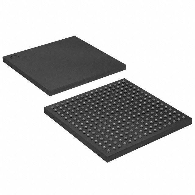
| 描述 | IC FPGA 358 I/O 484BGAFPGA - 现场可编程门阵列 17KLUTs 358 I/O Inst -on DSP 1.2V -5 Spd |
| 产品分类 | |
| I/O数 | 358 |
| LAB/CLB数 | 2125 |
| 品牌 | Lattice Semiconductor Corporation |
| 产品手册 | |
| 产品图片 |
|
| rohs | 符合RoHS无铅 / 符合限制有害物质指令(RoHS)规范要求 |
| 产品系列 | 嵌入式处理器和控制器,FPGA - 现场可编程门阵列,Lattice LFXP2-17E-6FN484CXP2 |
| mouser_ship_limit | 此产品可能需要其他文件才能从美国出口。 |
| 数据手册 | |
| 产品型号 | LFXP2-17E-6FN484C |
| PCN组件/产地 | |
| PCN设计/规格 | http://www.latticesemi.com/~/media/Documents/ProductChangeNotification/13/PCN03A-13_Alternate_Qualified_Assembly_Test%20Site_Material_Sets_ASE_Taiwan.ashx |
| 产品 | XP2 |
| 产品种类 | FPGA - 现场可编程门阵列 |
| 供应商器件封装 | 484-FPBGA(23x23) |
| 其它名称 | 220-1117 |
| 内嵌式块RAM-EBR | 276 kbit |
| 分布式RAM | 35 kbit |
| 商标 | Lattice |
| 安装类型 | 表面贴装 |
| 安装风格 | SMD/SMT |
| 封装 | Tray |
| 封装/外壳 | 484-BBGA |
| 封装/箱体 | FPBGA-484 |
| 工作温度 | 0°C ~ 85°C |
| 工作电源电压 | 1.2 V |
| 工厂包装数量 | 60 |
| 总RAM位数 | 282624 |
| 总内存 | 311 kbit |
| 最大工作温度 | + 85 C |
| 最小工作温度 | 0 C |
| 栅极数 | - |
| 标准包装 | 60 |
| 电压-电源 | 1.14 V ~ 1.26 V |
| 系列 | LFXP2-17E-6FN |
| 输入/输出端数量 | 358 |
| 逻辑元件/单元数 | 17000 |
| 逻辑元件数量 | 17000 |
| 逻辑数组块数量——LAB | 2125 |


- 商务部:美国ITC正式对集成电路等产品启动337调查
- 曝三星4nm工艺存在良率问题 高通将骁龙8 Gen1或转产台积电
- 太阳诱电将投资9.5亿元在常州建新厂生产MLCC 预计2023年完工
- 英特尔发布欧洲新工厂建设计划 深化IDM 2.0 战略
- 台积电先进制程称霸业界 有大客户加持明年业绩稳了
- 达到5530亿美元!SIA预计今年全球半导体销售额将创下新高
- 英特尔拟将自动驾驶子公司Mobileye上市 估值或超500亿美元
- 三星加码芯片和SET,合并消费电子和移动部门,撤换高东真等 CEO
- 三星电子宣布重大人事变动 还合并消费电子和移动部门
- 海关总署:前11个月进口集成电路产品价值2.52万亿元 增长14.8%
PDF Datasheet 数据手册内容提取
LatticeXP2™ Family Data Sheet DS1009 Version 2.3, June 2017
LatticeXP2 Family Data Sheet Introduction February 2012 Data Sheet DS1009 Features Flexible I/O Buffer (cid:129) sysIO™ buffer supports: flexiFLASH™ Architecture – LVCMOS 33/25/18/15/12; LVTTL • Instant-on – SSTL 33/25/18 class I, II (cid:129) Infinitely reconfigurable – HSTL15 class I; HSTL18 class I, II (cid:129) Single chip – PCI (cid:129) FlashBAK™ technology – LVDS, Bus-LVDS, MLVDS, LVPECL, RSDS (cid:129) Serial TAG memory Pre-engineered Source Synchronous (cid:129) Design security Interfaces Live Update Technology (cid:129) DDR / DDR2 interfaces up to 200 MHz (cid:129) TransFR™ technology (cid:129) 7:1 LVDS interfaces support display applications (cid:129) Secure updates with 128 bit AES encryption (cid:129) XGMII (cid:129) Dual-boot with external SPI Density And Package Options sysDSP™ Block (cid:129) 5k to 40k LUT4s, 86 to 540 I/Os (cid:129) Three to eight blocks for high performance (cid:129) csBGA, TQFP, PQFP, ftBGA and fpBGA packages Multiply and Accumulate (cid:129) Density migration supported (cid:129) 12 to 32 18x18 multipliers Flexible Device Configuration (cid:129) Each block supports one 36x36 multiplier or four (cid:129) SPI (master and slave) Boot Flash Interface 18x18 or eight 9x9 multipliers (cid:129) Dual Boot Image supported Embedded and Distributed Memory (cid:129) Soft Error Detect (SED) macro embedded (cid:129) Up to 885 Kbits sysMEM™ EBR System Level Support (cid:129) Up to 83 Kbits Distributed RAM (cid:129) IEEE 1149.1 and IEEE 1532 Compliant sysCLOCK™ PLLs (cid:129) On-chip oscillator for initialization & general use (cid:129) Up to four analog PLLs per device (cid:129) Devices operate with 1.2V power supply (cid:129) Clock multiply, divide and phase shifting Table 1-1. LatticeXP2 Family Selection Guide Device XP2-5 XP2-8 XP2-17 XP2-30 XP2-40 LUTs (K) 5 8 17 29 40 Distributed RAM (KBits) 10 18 35 56 83 EBR SRAM (KBits) 166 221 276 387 885 EBR SRAM Blocks 9 12 15 21 48 sysDSP Blocks 3 4 5 7 8 18 x 18 Multipliers 12 16 20 28 32 V Voltage 1.2 1.2 1.2 1.2 1.2 CC GPLL 2 2 4 4 4 Max Available I/O 172 201 358 472 540 Packages and I/O Combinations 132-Ball csBGA (8 x 8 mm) 86 86 144-Pin TQFP (20 x 20 mm) 100 100 208-Pin PQFP (28 x 28 mm) 146 146 146 256-Ball ftBGA (17 x17 mm) 172 201 201 201 484-Ball fpBGA (23 x 23 mm) 358 363 363 672-Ball fpBGA (27 x 27 mm) 472 540 © 2012 Lattice Semiconductor Corp. All Lattice trademarks, registered trademarks, patents, and disclaimers are as listed at www.latticesemi.com/legal. All other brand or product names are trademarks or registered trademarks of their respective holders. The specifications and information herein are subject to change without notice. www.latticesemi.com 1-1 DS1009 Introduction_01.4
Introduction LatticeXP2 Family Data Sheet Introduction LatticeXP2 devices combine a Look-up Table (LUT) based FPGA fabric with non-volatile Flash cells in an architec- ture referred to as flexiFLASH. The flexiFLASH approach provides benefits including instant-on, infinite reconfigurability, on chip storage with FlashBAK embedded block memory and Serial TAG memory and design security. The parts also support Live Update technology with TransFR, 128-bit AES Encryption and Dual-boot technologies. The LatticeXP2 FPGA fabric was optimized for the new technology from the outset with high performance and low cost in mind. LatticeXP2 devices include LUT-based logic, distributed and embedded memory, Phase Locked Loops (PLLs), pre-engineered source synchronous I/O support and enhanced sysDSP blocks. Lattice Diamond® design software allows large and complex designs to be efficiently implemented using the LatticeXP2 family of FPGA devices. Synthesis library support for LatticeXP2 is available for popular logic synthesis tools. The Diamond software uses the synthesis tool output along with the constraints from its floor planning tools to place and route the design in the LatticeXP2 device. The Diamond tool extracts the timing from the routing and back-annotates it into the design for timing verification. Lattice provides many pre-designed Intellectual Property (IP) LatticeCORE™ modules for the LatticeXP2 family. By using these IPs as standardized blocks, designers are free to concentrate on the unique aspects of their design, increasing their productivity. 1-2
LatticeXP2 Family Data Sheet Architecture August 2014 Data Sheet DS1009 Architecture Overview Each LatticeXP2 device contains an array of logic blocks surrounded by Programmable I/O Cells (PIC). Inter- spersed between the rows of logic blocks are rows of sysMEM™ Embedded Block RAM (EBR) and a row of sys- DSP™ Digital Signal Processing blocks as shown in Figure 2-1. On the left and right sides of the Programmable Functional Unit (PFU) array, there are Non-volatile Memory Blocks. In configuration mode the nonvolatile memory is programmed via the IEEE 1149.1 TAP port or the sysCONFIG™ peripheral port. On power up, the configuration data is transferred from the Non-volatile Memory Blocks to the con- figuration SRAM. With this technology, expensive external configuration memory is not required, and designs are secured from unauthorized read-back. This transfer of data from non-volatile memory to configuration SRAM via wide busses happens in microseconds, providing an “instant-on” capability that allows easy interfacing in many applications. LatticeXP2 devices can also transfer data from the sysMEM EBR blocks to the Non-volatile Memory Blocks at user request. There are two kinds of logic blocks, the PFU and the PFU without RAM (PFF). The PFU contains the building blocks for logic, arithmetic, RAM and ROM functions. The PFF block contains building blocks for logic, arithmetic and ROM functions. Both PFU and PFF blocks are optimized for flexibility allowing complex designs to be imple- mented quickly and efficiently. Logic Blocks are arranged in a two-dimensional array. Only one type of block is used per row. LatticeXP2 devices contain one or more rows of sysMEM EBR blocks. sysMEM EBRs are large dedicated 18Kbit memory blocks. Each sysMEM block can be configured in a variety of depths and widths of RAM or ROM. In addi- tion, LatticeXP2 devices contain up to two rows of DSP Blocks. Each DSP block has multipliers and adder/accumu- lators, which are the building blocks for complex signal processing capabilities. Each PIC block encompasses two PIOs (PIO pairs) with their respective sysIO buffers. The sysIO buffers of the LatticeXP2 devices are arranged into eight banks, allowing the implementation of a wide variety of I/O standards. PIO pairs on the left and right edges of the device can be configured as LVDS transmit/receive pairs. The PIC logic also includes pre-engineered support to aid in the implementation of high speed source synchronous standards such as 7:1 LVDS interfaces, found in many display applications, and memory interfaces including DDR and DDR2. The LatticeXP2 registers in PFU and sysI/O can be configured to be SET or RESET. After power up and device is configured, the device enters into user mode with these registers SET/RESET according to the configuration set- ting, allowing device entering to a known state for predictable system function. Other blocks provided include PLLs and configuration functions. The LatticeXP2 architecture provides up to four General Purpose PLLs (GPLL) per device. The GPLL blocks are located in the corners of the device. The configuration block that supports features such as configuration bit-stream de-encryption, transparent updates and dual boot support is located between banks two and three. Every device in the LatticeXP2 family supports a sysCONFIG port, muxed with bank seven I/Os, which supports serial device configuration. A JTAG port is provided between banks two and three. This family also provides an on-chip oscillator. LatticeXP2 devices use 1.2V as their core voltage. © 2014 Lattice Semiconductor Corp. All Lattice trademarks, registered trademarks, patents, and disclaimers are as listed at www.latticesemi.com/legal. All other brand or product names are trademarks or registered trademarks of their respective holders. The specifications and information herein are subject to change without notice. www.latticesemi.com 2-1 DS1009 Architecture_01.8
Architecture LatticeXP2 Family Data Sheet Figure 2-1. Simplified Block Diagram, LatticeXP2-17 Device (Top Level) sysIO Buffers, Pre-Engineered Source Synchronous Support On-chip Oscillator Programmable Function Units (PFUs) SPI Port sysMEM Block JTAG Port RAM DSP Blocks Flash sysCLOCK PLLs Flexible Routing PFU Blocks The core of the LatticeXP2 device is made up of logic blocks in two forms, PFUs and PFFs. PFUs can be pro- grammed to perform logic, arithmetic, distributed RAM and distributed ROM functions. PFF blocks can be pro- grammed to perform logic, arithmetic and ROM functions. Except where necessary, the remainder of this data sheet will use the term PFU to refer to both PFU and PFF blocks. Each PFU block consists of four interconnected slices, numbered Slice 0 through Slice 3, as shown in Figure 2-2. All the interconnections to and from PFU blocks are from routing. There are 50 inputs and 23 outputs associated with each PFU block. 2-2
Architecture LatticeXP2 Family Data Sheet Figure 2-2. PFU Diagram From Routing LUT4& LUT4& LUT4& LUT4& LUT4& LUT4& CARRY CARRY CARRY CARRY CARRY CARRY LUT4 LUT4 Slice 0 Slice 1 Slice 2 Slice 3 D D D D D D FF FF FF FF FF FF To Routing Slice Slice 0 through Slice 2 contain two 4-input combinatorial Look-Up Tables (LUT4), which feed two registers. Slice 3 contains two LUT4s and no registers. For PFUs, Slice 0 and Slice 2 can also be configured as distributed memory, a capability not available in PFF blocks. Table 2-1 shows the capability of the slices in both PFF and PFU blocks along with the operation modes they enable. In addition, each PFU contains logic that allows the LUTs to be com- bined to perform functions such as LUT5, LUT6, LUT7 and LUT8. There is control logic to perform set/reset func- tions (programmable as synchronous/asynchronous), clock select, chip-select and wider RAM/ROM functions. Figure 2-3 shows an overview of the internal logic of the slice. The registers in the slice can be configured as posi- tive/negative edge triggered or level sensitive clocks. Table 2-1. Resources and Modes Available per Slice PFU BLock PFF Block Slice Resources Modes Resources Modes Slice 0 2 LUT4s and 2 Registers Logic, Ripple, RAM, ROM 2 LUT4s and 2 Registers Logic, Ripple, ROM Slice 1 2 LUT4s and 2 Registers Logic, Ripple, ROM 2 LUT4s and 2 Registers Logic, Ripple, ROM Slice 2 2 LUT4s and 2 Registers Logic, Ripple, RAM, ROM 2 LUT4s and 2 Registers Logic, Ripple, ROM Slice 3 2 LUT4s Logic, ROM 2 LUT4s Logic, ROM Slice 0 through Slice 2 have 14 input signals: 13 signals from routing and one from the carry-chain (from the adja- cent slice or PFU). There are seven outputs: six to routing and one to carry-chain (to the adjacent PFU). Slice 3 has 13 input signals from routing and four signals to routing. Table 2-2 lists the signals associated with Slice 0 to Slice 2. 2-3
Architecture LatticeXP2 Family Data Sheet Figure 2-3. Slice Diagram FCO from Slice/PFU, FCI into Different Slice/PFU SLICE FXB OFX1 FXA A1 CO F1 B1 F/SUM C1 D1 LUT4 & D Q1 CARRY* FF* CI To Routing M1 M0 LUT5 From Mux Routing OFX0 A0 CO B0 C0 F0 D0 LUT4 & CARRY* F/SUM D Q0 FF* CI CE CLK LSR * Not in Slice 3 FCI into Slice/PFU, FCO from Different Slice/PFU For Slices 0 and 2, memory control signals are generated from Slice 1 as follows: WCK is CLK WRE is from LSR DI[3:2] for Slice 2 and DI[1:0] for Slice 0 data WAD [A:D] is a 4bit address from slice 1 LUT input Table 2-2. Slice Signal Descriptions Function Type Signal Names Description Input Data signal A0, B0, C0, D0 Inputs to LUT4 Input Data signal A1, B1, C1, D1 Inputs to LUT4 Input Multi-purpose M0 Multipurpose Input Input Multi-purpose M1 Multipurpose Input Input Control signal CE Clock Enable Input Control signal LSR Local Set/Reset Input Control signal CLK System Clock Input Inter-PFU signal FCI Fast Carry-In1 Input Inter-slice signal FXA Intermediate signal to generate LUT6 and LUT7 Input Inter-slice signal FXB Intermediate signal to generate LUT6 and LUT7 Output Data signals F0, F1 LUT4 output register bypass signals Output Data signals Q0, Q1 Register outputs Output Data signals OFX0 Output of a LUT5 MUX Output Data signals OFX1 Output of a LUT6, LUT7, LUT82 MUX depending on the slice Output Inter-PFU signal FCO Slice 2 of each PFU is the fast carry chain output1 1. See Figure 2-3 for connection details. 2. Requires two PFUs. 2-4
Architecture LatticeXP2 Family Data Sheet Modes of Operation Each slice has up to four potential modes of operation: Logic, Ripple, RAM and ROM. Logic Mode In this mode, the LUTs in each slice are configured as LUT4s. A LUT4 has 16 possible input combinations. Four- input logic functions are generated by programming the LUT4. Since there are two LUT4s per slice, a LUT5 can be constructed within one slice. Larger LUTs such as LUT6, LUT7 and LUT8, can be constructed by concatenating two or more slices. Note that a LUT8 requires more than four slices. Ripple Mode Ripple mode allows efficient implementation of small arithmetic functions. In ripple mode, the following functions can be implemented by each slice: (cid:129) Addition 2-bit (cid:129) Subtraction 2-bit (cid:129) Add/Subtract 2-bit using dynamic control (cid:129) Up counter 2-bit (cid:129) Down counter 2-bit (cid:129) Up/Down counter with async clear (cid:129) Up/Down counter with preload (sync) (cid:129) Ripple mode multiplier building block (cid:129) Multiplier support (cid:129) Comparator functions of A and B inputs – A greater-than-or-equal-to B – A not-equal-to B – A less-than-or-equal-to B Two carry signals, FCI and FCO, are generated per slice in this mode, allowing fast arithmetic functions to be con- structed by concatenating slices. RAM Mode In this mode, a 16x4-bit distributed Single Port RAM (SPR) can be constructed using each LUT block in Slice 0 and Slice 2 as a 16x1-bit memory. Slice 1 is used to provide memory address and control signals. A 16x2-bit Pseudo Dual Port RAM (PDPR) memory is created by using one slice as the read-write port and the other companion slice as the read-only port. The Lattice design tools support the creation of a variety of different size memories. Where appropriate, the soft- ware will construct these using distributed memory primitives that represent the capabilities of the PFU. Table 2-3 shows the number of slices required to implement different distributed RAM primitives. For more information on using RAM in LatticeXP2 devices, please see TN1137, LatticeXP2 Memory Usage Guide. Table 2-3. Number of Slices Required For Implementing Distributed RAM SPR 16X4 PDPR 16X4 Number of slices 3 3 Note: SPR = Single Port RAM, PDPR = Pseudo Dual Port RAM ROM Mode ROM mode uses the LUT logic; hence, Slices 0 through 3 can be used in the ROM mode. Preloading is accom- plished through the programming interface during PFU configuration. 2-5
Architecture LatticeXP2 Family Data Sheet Routing There are many resources provided in the LatticeXP2 devices to route signals individually or as busses with related control signals. The routing resources consist of switching circuitry, buffers and metal interconnect (routing) seg- ments. The inter-PFU connections are made with x1 (spans two PFU), x2 (spans three PFU) or x6 (spans seven PFU) connections. The x1 and x2 connections provide fast and efficient connections in horizontal and vertical directions. The x2 and x6 resources are buffered to allow both short and long connections routing between PFUs. The LatticeXP2 family has an enhanced routing architecture to produce a compact design. The Diamond design tool takes the output of the synthesis tool and places and routes the design. Generally, the place and route tool is completely automatic, although an interactive routing editor is available to optimize the design. sysCLOCK Phase Locked Loops (PLL) The sysCLOCK PLLs provide the ability to synthesize clock frequencies. The LatticeXP2 family supports between two and four full featured General Purpose PLLs (GPLL). The architecture of the GPLL is shown in Figure 2-4. CLKI, the PLL reference frequency, is provided either from the pin or from routing; it feeds into the Input Clock Divider block. CLKFB, the feedback signal, is generated from CLKOP (the primary clock output) or from a user clock pin/logic. CLKFB feeds into the Feedback Divider and is used to multiply the reference frequency. Both the input path and feedback signals enter the Voltage Controlled Oscillator (VCO) block. The phase and fre- quency of the VCO are determined from the input path and feedback signals. A LOCK signal is generated by the VCO to indicate that the VCO is locked with the input clock signal. The output of the VCO feeds into the CLKOP Divider, a post-scalar divider. The duty cycle of the CLKOP Divider output can be fine tuned using the Duty Trim block, which creates the CLKOP signal. By allowing the VCO to oper- ate at higher frequencies than CLKOP, the frequency range of the GPLL is expanded. The output of the CLKOP Divider is passed through the CLKOK Divider, a secondary clock divider, to generate lower frequencies for the CLKOK output. For applications that require even lower frequencies, the CLKOP signal is passed through a divide- by-three divider to produce the CLKOK2 output. The CLKOK2 output is provided for applications that use source synchronous logic. The Phase/Duty Cycle/Duty Trim block is used to adjust the phase and duty cycle of the CLKOP Divider output to generate the CLKOS signal. The phase/duty cycle setting can be pre-programmed or dynamically adjusted. The clock outputs from the GPLL; CLKOP, CLKOK, CLKOK2 and CLKOS, are fed to the clock distribution network. For further information on the GPLL please see TN1126, LatticeXP2 sysCLOCK PLL Design and Usage Guide. 2-6
Architecture LatticeXP2 Family Data Sheet Figure 2-4. General Purpose PLL (GPLL) Diagram WRDEL DDUTY DPHASE CLKOK2 3 Phase/ CLKOS CLKI CLKI Duty Cycle/ Divider Duty Trim VCO/ CLKOP PFD LOOP FILTER Divider CLKOP CLKFB CLKFB Duty Trim Divider CLKOK CLKOK Divider Internal Feedback RSTK Lock LOCK RST Detect Table 2-4 provides a description of the signals in the GPLL blocks. Table 2-4. GPLL Block Signal Descriptions Signal I/O Description CLKI I Clock input from external pin or routing PLL feedback input from CLKOP (PLL internal), from clock net (CLKOP) or from a user clock CLKFB I (PIN or logic) RST I “1” to reset PLL counters, VCO, charge pumps and M-dividers RSTK I “1” to reset K-divider DPHASE [3:0] I DPA Phase Adjust input DDDUTY [3:0] I DPA Duty Cycle Select input WRDEL I DPA Fine Delay Adjust input CLKOS O PLL output clock to clock tree (phase shifted/duty cycle changed) CLKOP O PLL output clock to clock tree (no phase shift) CLKOK O PLL output to clock tree through secondary clock divider CLKOK2 O PLL output to clock tree (CLKOP divided by 3) LOCK O “1” indicates PLL LOCK to CLKI Clock Dividers LatticeXP2 devices have two clock dividers, one on the left side and one on the right side of the device. These are intended to generate a slower-speed system clock from a high-speed edge clock. The block operates in a ÷2, ÷4 or ÷8 mode and maintains a known phase relationship between the divided down clock and the high-speed clock based on the release of its reset signal. The clock dividers can be fed from the CLKOP output from the GPLLs or from the Edge Clocks (ECLK). The clock divider outputs serve as primary clock sources and feed into the clock dis- tribution network. The Reset (RST) control signal resets the input and forces all outputs to low. The RELEASE sig- nal releases outputs to the input clock. For further information on clock dividers, please see TN1126, LatticeXP2 sysCLOCK PLL Design and Usage Guide. Figure 2-5 shows the clock divider connections. 2-7
Architecture LatticeXP2 Family Data Sheet Figure 2-5. Clock Divider Connections ECLK ÷1 CLKOP (GPLL) ÷2 CLKDIV ÷4 RST RELEASE ÷8 Clock Distribution Network LatticeXP2 devices have eight quadrant-based primary clocks and between six and eight flexible region-based sec- ondary clocks/control signals. Two high performance edge clocks are available on each edge of the device to sup- port high speed interfaces. The clock inputs are selected from external I/Os, the sysCLOCK PLLs, or routing. Clock inputs are fed throughout the chip via the primary, secondary and edge clock networks. Primary Clock Sources LatticeXP2 devices derive primary clocks from four sources: PLL outputs, CLKDIV outputs, dedicated clock inputs and routing. LatticeXP2 devices have two to four sysCLOCK PLLs, located in the four corners of the device. There are eight dedicated clock inputs, two on each side of the device. Figure 2-6 shows the primary clock sources. 2-8
Architecture LatticeXP2 Family Data Sheet Figure 2-6. Primary Clock Sources for XP2-17 Clock Input Clock Input From Routing PLL Input GPLL GPLL PLL Input CLK CLK DIV DIV Clock Primary Clock Sources Clock Input Input to Eight Quadrant Clock Selection Clock Clock Input Input PLL Input GPLL GPLL PLL Input From Routing Clock Input Clock Input Note: This diagram shows sources for the XP2-17 device. Smaller LatticeXP2 devices have two GPLLs. 2-9
Architecture LatticeXP2 Family Data Sheet Secondary Clock/Control Sources LatticeXP2 devices derive secondary clocks (SC0 through SC7) from eight dedicated clock input pads and the rest from routing. Figure 2-7 shows the secondary clock sources. Figure 2-7. Secondary Clock Sources Clock Clock Input Input From From From From Routing Routing Routing Routing From Routing From Routing From Routing From Routing Clock Input Clock Input Secondary Clock Sources Clock Input Clock Input From Routing From Routing From Routing From Routing From From From From Routing Routing Routing Routing Clock Clock Input Input 2-10
Architecture LatticeXP2 Family Data Sheet Edge Clock Sources Edge clock resources can be driven from a variety of sources at the same edge. Edge clock resources can be driven from adjacent edge clock PIOs, primary clock PIOs, PLLs and clock dividers as shown in Figure 2-8. Figure 2-8. Edge Clock Sources Clock Input Clock Input From From Routing Routing Sources for top edge clocks CLKOP CLKOP PLL PLL Input GPLL CLKOS CLKOS GPLL Input From Routing From Routing Clock Clock Input Input Eight Edge Clocks (ECLK) Clock Two Clocks per Edge Clock Input Input From Routing From Routing CLKOP CLKOP PLL PLL Input GPLL CLKOS CLKOSGPLL Input Sources for left edge clocks Sources for right edge clocks Sources for bottom edge clocks From From Routing Routing Clock Input Clock Input Note: This diagram shows sources for the XP2-17 device. Smaller LatticeXP2 devices have two GPLLs. 2-11
Architecture LatticeXP2 Family Data Sheet Primary Clock Routing The clock routing structure in LatticeXP2 devices consists of a network of eight primary clock lines (CLK0 through CLK7) per quadrant. The primary clocks of each quadrant are generated from muxes located in the center of the device. All the clock sources are connected to these muxes. Figure 2-9 shows the clock routing for one quadrant. Each quadrant mux is identical. If desired, any clock can be routed globally. Figure 2-9. Per Quadrant Primary Clock Selection Primary Clock Sources: PLLs + CLKDIVs + PIOs + Routing 30:1 30:1 30:1 30:1 30:1 30:1 29:1 29:1 29:1 29:1 DCS DCS CLK0 CLK1 CLK2 CLK3 CLK4 CLK5 CLK6 CLK7 8 Primary Clocks (CLK0 to CLK7) per Quadrant Dynamic Clock Select (DCS) The DCS is a smart multiplexer function available in the primary clock routing. It switches between two independent input clock sources without any glitches or runt pulses. This is achieved irrespective of when the select signal is toggled. There are two DCS blocks per quadrant; in total, eight DCS blocks per device. The inputs to the DCS block come from the center muxes. The output of the DCS is connected to primary clocks CLK6 and CLK7 (see Figure 2- 9). Figure 2-10 shows the timing waveforms of the default DCS operating mode. The DCS block can be programmed to other modes. For more information on the DCS, please see TN1126, LatticeXP2 sysCLOCK PLL Design and Usage Guide. Figure 2-10. DCS Waveforms CLK0 CLK1 SEL DCSOUT Secondary Clock/Control Routing Secondary clocks in the LatticeXP2 devices are region-based resources. The benefit of region-based resources is the relatively low injection delay and skew within the region, as compared to primary clocks. EBR rows, DSP rows and a special vertical routing channel bound the secondary clock regions. This special vertical routing channel aligns with either the left edge of the center DSP block in the DSP row or the center of the DSP row. Figure 2-11 shows this special vertical routing channel and the eight secondary clock regions for the LatticeXP2-40. 2-12
Architecture LatticeXP2 Family Data Sheet LatticeXP2-30 and smaller devices have six secondary clock regions. All devices in the LatticeXP2 family have four secondary clocks (SC0 to SC3) which are distributed to every region. The secondary clock muxes are located in the center of the device. Figure 2-12 shows the mux structure of the secondary clock routing. Secondary clocks SC0 to SC3 are used for clock and control and SC4 to SC7 are used for high fan-out signals. Figure 2-11. Secondary Clock Regions XP2-40 I/O Bank 0 I/O Bank 1 Vertical Routing Channel Regional Boundary Secondary Clock Secondary Clock k 7 Region 1 Region 5 I/O ERBegRi oRnoawl Ban Ba Boundary O nk I/ 2 Secondary Clock Secondary Clock Region 2 Region 6 Secondary Clock Secondary Clock EBR Row Region 3 Region 7 Regional k 6 I/O Boundary an B B a O nk I/ Secondary Clock Secondary Clock 3 Region 4 Region 8 DSP Row Regional Boundary I/O Bank 5 I/O Bank 4 2-13
Architecture LatticeXP2 Family Data Sheet Figure 2-12. Secondary Clock Selection Secondary Clock Feedlines: 8 PIOs + 16 Routing 24:1 24:1 24:1 24:1 24:1 24:1 24:1 24:1 SC0 SC1 SC2 SC3 SC4 SC5 SC6 SC7 4 Secondary Clocks/CE/LSR (SC0 to SC3) per Region Clock/Control 4 High Fan-out Data Signals (SC4 to SC7) per Region High Fan-out Data Slice Clock Selection Figure 2-13 shows the clock selections and Figure 2-14 shows the control selections for Slice0 through Slice2. All the primary clocks and the four secondary clocks are routed to this clock selection mux. Other signals, via routing, can be used as clock inputs to the slices. Slice controls are generated from the secondary clocks or other signals connected via routing. If none of the signals are selected for both clock and control, then the default value of the mux output is 1. Slice 3 does not have any registers; therefore it does not have the clock or control muxes. Figure 2-13. Slice0 through Slice2 Clock Selection Primary Clock 8 Secondary Clock 4 Clock to Slice 25:1 Routing 12 Vcc 1 2-14
Architecture LatticeXP2 Family Data Sheet Figure 2-14. Slice0 through Slice2 Control Selection Secondary Clock 3 Slice Control Routing 16:1 12 Vcc 1 Edge Clock Routing LatticeXP2 devices have eight high-speed edge clocks that are intended for use with the PIOs in the implementa- tion of high-speed interfaces. Each device has two edge clocks per edge. Figure 2-15 shows the selection muxes for these clocks. Figure 2-15. Edge Clock Mux Connections Top and Bottom Clock Input Pad Edge Clocks ECLK1/ ECLK2 (Both Muxes) Routing Left and Right Input Pad Edge Clocks GPLL Input Pad ECLK1 GPLL Output CLKOP Routing Left and Right Input Pad Edge Clocks GPLL Input Pad ECLK2 GPLL Output CLKOS Routing 2-15
Architecture LatticeXP2 Family Data Sheet sysMEM Memory LatticeXP2 devices contains a number of sysMEM Embedded Block RAM (EBR). The EBR consists of 18 Kbit RAM with dedicated input and output registers. sysMEM Memory Block The sysMEM block can implement single port, dual port or pseudo dual port memories. Each block can be used in a variety of depths and widths as shown in Table 2-5. FIFOs can be implemented in sysMEM EBR blocks by using support logic with PFUs. The EBR block supports an optional parity bit for each data byte to facilitate parity check- ing. EBR blocks provide byte-enable support for configurations with18-bit and 36-bit data widths. Table 2-5. sysMEM Block Configurations Memory Mode Configurations 16,384 x 1 8,192 x 2 4,096 x 4 Single Port 2,048 x 9 1,024 x 18 512 x 36 16,384 x 1 8,192 x 2 True Dual Port 4,096 x 4 2,048 x 9 1,024 x 18 16,384 x 1 8,192 x 2 4,096 x 4 Pseudo Dual Port 2,048 x 9 1,024 x 18 512 x 36 Bus Size Matching All of the multi-port memory modes support different widths on each of the ports. The RAM bits are mapped LSB word 0 to MSB word 0, LSB word 1 to MSB word 1, and so on. Although the word size and number of words for each port varies, this mapping scheme applies to each port. FlashBAK EBR Content Storage All the EBR memory in the LatticeXP2 is shadowed by Flash memory. Optionally, initialization values for the mem- ory blocks can be defined using the Lattice Diamond design tools. The initialization values are loaded into the Flash memory during device programming and into the SRAM at power up or whenever the device is reconfigured. This feature is ideal for the storage of a variety of information such as look-up tables and microprocessor code. It is also possible to write the current contents of the EBR memory back to Flash memory. This capability is useful for the storage of data such as error codes and calibration information. For additional information on the FlashBAK capa- bility see TN1137, LatticeXP2 Memory Usage Guide. 2-16
Architecture LatticeXP2 Family Data Sheet Figure 2-16. FlashBAK Technology Write to Flash During Make Infinite Reads and Programming Writes to EBR Flash JTAG / SPI Port FPGA Logic EBR Write From Flash to EBR During Configuration / Write From EBR to Flash on User Command Memory Cascading Larger and deeper blocks of RAMs can be created using EBR sysMEM Blocks. Typically, the Lattice design tools cascade memory transparently, based on specific design inputs. Single, Dual and Pseudo-Dual Port Modes In all the sysMEM RAM modes the input data and address for the ports are registered at the input of the memory array. The output data of the memory is optionally registered at the output. EBR memory supports two forms of write behavior for single port or dual port operation: 1. Normal – Data on the output appears only during a read cycle. During a write cycle, the data (at the current address) does not appear on the output. This mode is supported for all data widths. 2. Write Through – A copy of the input data appears at the output of the same port during a write cycle. This mode is supported for all data widths. Memory Core Reset The memory array in the EBR utilizes latches at the A and B output ports. These latches can be reset asynchro- nously or synchronously. RSTA and RSTB are local signals, which reset the output latches associated with Port A and Port B respectively. GSRN, the global reset signal, resets both ports. The output data latches and associated resets for both ports are as shown in Figure 2-17. Figure 2-17. Memory Core Reset Memory Core DSETQ Port A[17:0] LCLR Output Data Latches DSETQ Port B[17:0] LCLR RSTA RSTB GSRN Programmable Disable 2-17
Architecture LatticeXP2 Family Data Sheet For further information on the sysMEM EBR block, please see TN1137, LatticeXP2 Memory Usage Guide. EBR Asynchronous Reset EBR asynchronous reset or GSR (if used) can only be applied if all clock enables are low for a clock cycle before the reset is applied and released a clock cycle after the low-to-high transition of the reset signal, as shown in Figure 2-18. The GSR input to the EBR is always asynchronous. Figure 2-18. EBR Asynchronous Reset (Including GSR) Timing Diagram Reset Clock Clock Enable If all clock enables remain enabled, the EBR asynchronous reset or GSR may only be applied and released after the EBR read and write clock inputs are in a steady state condition for a minimum of 1/f (EBR clock). The reset MAX release must adhere to the EBR synchronous reset setup time before the next active read or write clock edge. If an EBR is pre-loaded during configuration, the GSR input must be disabled or the release of the GSR during device Wake Up must occur before the release of the device I/Os becoming active. These instructions apply to all EBR RAM and ROM implementations. Note that there are no reset restrictions if the EBR synchronous reset is used and the EBR GSR input is disabled. sysDSP™ Block The LatticeXP2 family provides a sysDSP block making it ideally suited for low cost, high performance Digital Sig- nal Processing (DSP) applications. Typical functions used in these applications include Bit Correlators, Fast Fourier Transform (FFT) functions, Finite Impulse Response (FIR) Filter, Reed-Solomon Encoder/Decoder, Turbo Encoder/ Decoder and Convolutional Encoder/Decoder. These complex signal processing functions use similar building blocks such as multiply-adders and multiply-accumulators. sysDSP Block Approach Compare to General DSP Conventional general-purpose DSP chips typically contain one to four (Multiply and Accumulate) MAC units with fixed data-width multipliers; this leads to limited parallelism and limited throughput. Their throughput is increased by higher clock speeds. The LatticeXP2 family, on the other hand, has many DSP blocks that support different data- widths. This allows the designer to use highly parallel implementations of DSP functions. The designer can opti- mize the DSP performance vs. area by choosing appropriate levels of parallelism. Figure 2-19 compares the fully serial and the mixed parallel and serial implementations. 2-18
Architecture LatticeXP2 Family Data Sheet Figure 2-19. Comparison of General DSP and LatticeXP2 Approaches Operand Operand Operand A A A Operand Operand Operand B B B Operand Operand A B x x x m/k Multiplier 0 loops x Multiplier 1 Single M loops Multiplier k Multiplier Accumulator ++ (k adds) Function implemented in General purpose DSP m/k accumulate Output Function implemented in LatticeXP2 sysDSP Block Capabilities The sysDSP block in the LatticeXP2 family supports four functional elements in three 9, 18 and 36 data path widths. The user selects a function element for a DSP block and then selects the width and type (signed/unsigned) of its operands. The operands in the LatticeXP2 family sysDSP Blocks can be either signed or unsigned but not mixed within a function element. Similarly, the operand widths cannot be mixed within a block. DSP elements can be concatenated. The resources in each sysDSP block can be configured to support the following four elements: (cid:129) MULT (Multiply) (cid:129) MAC (Multiply, Accumulate) (cid:129) MULTADDSUB (Multiply, Addition/Subtraction) (cid:129) MULTADDSUBSUM (Multiply, Addition/Subtraction, Accumulate) The number of elements available in each block depends on the width selected from the three available options: x9, x18, and x36. A number of these elements are concatenated for highly parallel implementations of DSP functions. Table 2-6 shows the capabilities of the block. Table 2-6. Maximum Number of Elements in a Block Width of Multiply x9 x18 x36 MULT 8 4 1 MAC 2 2 — MULTADDSUB 4 2 — MULTADDSUBSUM 2 1 — Some options are available in four elements. The input register in all the elements can be directly loaded or can be loaded as shift register from previous operand registers. By selecting ‘dynamic operation’ the following operations are possible: 2-19
Architecture LatticeXP2 Family Data Sheet (cid:129) In the ‘Signed/Unsigned’ options the operands can be switched between signed and unsigned on every cycle. (cid:129) In the ‘Add/Sub’ option the Accumulator can be switched between addition and subtraction on every cycle. (cid:129) The loading of operands can switch between parallel and serial operations. MULT sysDSP Element This multiplier element implements a multiply with no addition or accumulator nodes. The two operands, A and B, are multiplied and the result is available at the output. The user can enable the input/output and pipeline registers. Figure 2-20 shows the MULT sysDSP element. Figure 2-20. MULT sysDSP Element Shift Register B In Shift Register A In Multiplicand m m Multiplier n m n Input Data m Multiplier m+n n Register A x (default) putster m+n utgi Input Data n ORe Output Register B Pipeline m Register n Signed A Input To Register Multiplier Signed B Input To CLK (CLK0,CLK1,CLK2,CLK3) Register Multiplier CE (CE0,CE1,CE2,CE3) RST(RST0,RST1,RST2,RST3) Shift Register B Out Shift Register A Out 2-20
Architecture LatticeXP2 Family Data Sheet MAC sysDSP Element In this case, the two operands, A and B, are multiplied and the result is added with the previous accumulated value. This accumulated value is available at the output. The user can enable the input and pipeline registers but the out- put register is always enabled. The output register is used to store the accumulated value. The Accumulators in the DSP blocks in LatticeXP2 family can be initialized dynamically. A registered overflow signal is also available. The overflow conditions are provided later in this document. Figure 2-21 shows the MAC sysDSP element. Figure 2-21. MAC sysDSP Serial Register B in Serial Register A in Preload Multiplicand m m Accumulator m Multiplier n n r m+n+16 n RInepguits tDear tAa m Mxultiplier Outputegiste (default) Output m+n m+n+16 R Input Data n (default) (default) Register B Pipeline n Register r n putste Signed A ReIngpisutter RPeipgeislitneer To Accumulator OutRegi Overflow signal Signed B Input Pipeline Register Register To Accumulator Addn Input Pipeline To Accumulator Register Register CLK (CLK0,CLK1,CLK2,CLK3) Accumsload Input Pipeline Register Register To Accumulator CE (CE0,CE1,CE2,CE3) RST(RST0,RST1,RST2,RST3) SROB SROA 2-21
Architecture LatticeXP2 Family Data Sheet MULTADDSUB sysDSP Element In this case, the operands A0 and B0 are multiplied and the result is added/subtracted with the result of the multi- plier operation of operands A1 and B1. The user can enable the input, output and pipeline registers. Figure 2-22 shows the MULTADDSUB sysDSP element. Figure 2-22. MULTADDSUB Shift Register B In Shift Register A In Multiplicand A0 m m CLK (CLK0,CLK1,CLK2,CLK3) CE (CE0,CE1,CE2,CE3) Multiplier B0 n n m RST (RST0,RST1,RST2,RST3) Input Data m Multiplier n Register A x m+n Input Data n (default) Register B Pipeline m Register Add/Sub n Multiplicand A1 m putster Output m (mde+fanu+l1t) OutRegi (mde+fanu+l1t) Multiplier B1 n Input Data m Multiplier m+n n Register A x (default) Input Data n Register B Pipeline m Register n Signed A Input PipPeilpinee Register RegRisetger To Add/Sub Signed B Input PipPeilpinee Register RegRisetger To Add/Sub Addn Input PipePliipnee To Add/Sub Register RegRisetger Shift Register B Out Shift Register A Out 2-22
Architecture LatticeXP2 Family Data Sheet MULTADDSUBSUM sysDSP Element In this case, the operands A0 and B0 are multiplied and the result is added/subtracted with the result of the multi- plier operation of operands A1 and B1. Additionally the operands A2 and B2 are multiplied and the result is added/ subtracted with the result of the multiplier operation of operands A3 and B3. The result of both addition/subtraction are added in a summation block. The user can enable the input, output and pipeline registers. Figure 2-23 shows the MULTADDSUBSUM sysDSP element. Figure 2-23. MULTADDSUBSUM Shift Register B In Shift Register A In Multiplicand A0 m m CLK (CLK0,CLK1,CLK2,CLK3) Multiplier B0 n n m CE (CE0,CE1,CE2,CE3) Input Data m Multiplier m+n RST(RST0,RST1,RST2,RST3) n Register A x (default) Input Data n Register B Pipeline m Register Add/Sub0 n Multiplicand A1 m m+n (default) m Multiplier B1 n Input Data n Multiplier n Register A x m+n+1 Input Data n Register B Pipeline SUM Register Multiplicand A2 m m putster Output m+n+2 OutRegi m+n+2 Multiplier B2 n n m Input Data m Multiplier m+n n Register A x (default) Input Data n m+n+1 Register B m RPeipgeislitneer Add/Sub1 n Multiplicand A3 m m+n (default) m Multiplier B3 n Input Data m Multiplier n Register A x Input Data n Register B Pipeline m Register Signed A n Input Pipeline Register Register To Add/Sub0, Add/Sub1 Signed B Input Pipeline Register Register To Add/Sub0, Add/Sub1 Addn0 Input Pipeline Register Register To Add/Sub0 Addn1 Input Pipeline To Add/Sub1 Register Register Shift Register B Out Shift Register A Out Clock, Clock Enable and Reset Resources Global Clock, Clock Enable (CE) and Reset (RST) signals from routing are available to every DSP block. From four clock sources (CLK0, CLK1, CLK2, CLK3) one clock is selected for each input register, pipeline register and output 2-23
Architecture LatticeXP2 Family Data Sheet register. Similarly, CE and RST are selected from their four respective sources (CE0, CE1, CE2, CE3 and RST0, RST1, RST2, RST3) at each input register, pipeline register and output register. Signed and Unsigned with Different Widths The DSP block supports other widths, in addition to x9, x18 and x36 widths, of signed and unsigned multipliers. For unsigned operands, unused upper data bits should be filled to create a valid x9, x18 or x36 operand. For signed two’s complement operands, sign extension of the most significant bit should be performed until x9, x18 or x36 width is reached. Table 2-7 provides an example of this. Table 2-7. Sign Extension Example Unsigned Unsigned Two’s Complement Two’s Complement Number Unsigned 9-bit 18-bit Signed Signed 9 Bits Signed 18 Bits +5 0101 000000101 000000000000000101 0101 000000101 000000000000000101 -6 N/A N/A N/A 1010 111111010 111111111111111010 OVERFLOW Flag from MAC The sysDSP block provides an overflow output to indicate that the accumulator has overflowed. “Roll-over” occurs and an overflow signal is indicated when any of the following is true: two unsigned numbers are added and the result is a smaller number than the accumulator, two positive numbers are added with a negative sum or two nega- tive numbers are added with a positive sum. Note that when overflow occurs the overflow flag is present for only one cycle. By counting these overflow pulses in FPGA logic, larger accumulators can be constructed. The condi- tions for the overflow signal for signed and unsigned operands are listed in Figure 2-24. Figure 2-24. Accumulator Overflow/Underflow 011111100 252 000000011 3 001111111111110110 225543 000000000000000110 12 Carroyn seig cnyacll eis wgheenne rtahtiesd for 011111111 255 000000000 0 boundary is crossed 100000000 256 111111111 511 257 100000001 111111110 510 258 100000010 111111101 509 Unsigned Operation 011111100 252 000000011 +3 000000010 +2 Overflow signal is generated 011111101 253 000000001 +1 for one cycle when this 011111110 254 boundary is crossed 011111111 255 101010101010101010 -01 100000000 -256 111111110 -2 100000001 -255 111111101 -3 100000010 -254 Signed Operation 2-24
Architecture LatticeXP2 Family Data Sheet IPexpress™ The user can access the sysDSP block via the Lattice IPexpress tool, which provides the option to configure each DSP module (or group of modules), or by direct HDL instantiation. In addition, Lattice has partnered with The Math- Works® to support instantiation in the Simulink® tool, a graphical simulation environment. Simulink works with Dia- mond to dramatically shorten the DSP design cycle in Lattice FPGAs. Optimized DSP Functions Lattice provides a library of optimized DSP IP functions. Some of the IP cores planned for the LatticeXP2 DSP include the Bit Correlator, FFT functions, FIR Filter, Reed-Solomon Encoder/Decoder, Turbo Encoder/Decoder and Convolutional Encoder/Decoder. Please contact Lattice to obtain the latest list of available DSP IP cores. Resources Available in the LatticeXP2 Family Table 2-8 shows the maximum number of multipliers for each member of the LatticeXP2 family. Table 2-9 shows the maximum available EBR RAM Blocks and Serial TAG Memory bits in each LatticeXP2 device. EBR blocks, together with Distributed RAM can be used to store variables locally for fast DSP operations. Table 2-8. Maximum Number of DSP Blocks in the LatticeXP2 Family Device DSP Block 9x9 Multiplier 18x18 Multiplier 36x36 Multiplier XP2-5 3 24 12 3 XP2-8 4 32 16 4 XP2-17 5 40 20 5 XP2-30 7 56 28 7 XP2-40 8 64 32 8 Table 2-9. Embedded SRAM/TAG Memory in the LatticeXP2 Family Total EBR SRAM TAG Memory Device EBR SRAM Block (Kbits) (Bits) XP2-5 9 166 632 XP2-8 12 221 768 XP2-17 15 276 2184 XP2-30 21 387 2640 XP2-40 48 885 3384 LatticeXP2 DSP Performance Table 2-10 lists the maximum performance in Millions of MAC (MMAC) operations per second for each member of the LatticeXP2 family. Table 2-10. DSP Performance DSP Performance Device DSP Block MMAC XP2-5 3 3,900 XP2-8 4 5,200 XP2-17 5 6,500 XP2-30 7 9,100 XP2-40 8 10,400 For further information on the sysDSP block, please see TN1140, LatticeXP2 sysDSP Usage Guide. 2-25
Architecture LatticeXP2 Family Data Sheet Programmable I/O Cells (PIC) Each PIC contains two PIOs connected to their respective sysIO buffers as shown in Figure 2-25. The PIO Block supplies the output data (DO) and the tri-state control signal (TO) to the sysIO buffer and receives input from the buffer. Table 2-11 provides the PIO signal list. Figure 2-25. PIC Diagram PIOA TD OPOS1 ONEG1 IOLT0 Tristate Register Block OPOS0 PADA OPOS21 “T” ONEG0 ONEG21 IOLD0 Output Register Block sysIO Buffer QNEG01 QNEG11 QPOS01 QPOS11 INCK2 INDD INFF IPOS0 DI IPOS1 Input Control Register CLK Muxes Block CE CLK1 LSR CEO GSRN LSR ECLK1 GSR ECLK2 CLK0 DDRCLKPOL1 CEI DQSXFER1 DQS DEL PADB “C” PIOB 1. Signals are available on left/right/bottom edges only. 2. Selected blocks. Two adjacent PIOs can be joined to provide a differential I/O pair (labeled as “T” and “C”) as shown in Figure 2-25. The PAD Labels “T” and “C” distinguish the two PIOs. Approximately 50% of the PIO pairs on the left and right edges of the device can be configured as true LVDS outputs. All I/O pairs can operate as inputs. 2-26
Architecture LatticeXP2 Family Data Sheet Table 2-11. PIO Signal List Name Type Description CE Control from the core Clock enables for input and output block flip-flops CLK Control from the core System clocks for input and output blocks ECLK1, ECLK2 Control from the core Fast edge clocks LSR Control from the core Local Set/Reset GSRN Control from routing Global Set/Reset (active low) INCK2 Input to the core Input to Primary Clock Network or PLL reference inputs DQS Input to PIO DQS signal from logic (routing) to PIO INDD Input to the core Unregistered data input to core INFF Input to the core Registered input on positive edge of the clock (CLK0) IPOS0, IPOS1 Input to the core Double data rate registered inputs to the core QPOS01, QPOS11 Input to the core Gearbox pipelined inputs to the core QNEG01, QNEG11 Input to the core Gearbox pipelined inputs to the core OPOS0, ONEG0, Output data from the core Output signals from the core for SDR and DDR operation OPOS2, ONEG2 OPOS1 ONEG1 Tristate control from the core Signals to Tristate Register block for DDR operation DEL[3:0] Control from the core Dynamic input delay control bits TD Tristate control from the core Tristate signal from the core used in SDR operation DDRCLKPOL Control from clock polarity bus Controls the polarity of the clock (CLK0) that feed the DDR input block DQSXFER Control from core Controls signal to the Output block 1. Signals available on left/right/bottom only. 2. Selected I/O. PIO The PIO contains four blocks: an input register block, output register block, tristate register block and a control logic block. These blocks contain registers for operating in a variety of modes along with necessary clock and selection logic. Input Register Block The input register blocks for PIOs contain delay elements and registers that can be used to condition high-speed interface signals, such as DDR memory interfaces and source synchronous interfaces, before they are passed to the device core. Figure 2-26 shows the diagram of the input register block. Input signals are fed from the sysIO buffer to the input register block (as signal DI). If desired, the input signal can bypass the register and delay elements and be used directly as a combinatorial signal (INDD), a clock (INCK) and, in selected blocks, the input to the DQS delay block. If an input delay is desired, designers can select either a fixed delay or a dynamic delay DEL[3:0]. The delay, if selected, reduces input register hold time requirements when using a global clock. The input block allows three modes of operation. In the Single Data Rate (SDR) mode, the data is registered, by one of the registers in the SDR Sync register block, with the system clock. In DDR mode two registers are used to sample the data on the positive and negative edges of the DQS signal which creates two data streams, D0 and D2. D0 and D2 are synchronized with the system clock before entering the core. Further information on this topic can be found in the DDR Memory Support section of this data sheet. By combining input blocks of the complementary PIOs and sharing registers from output blocks, a gearbox function can be implemented, that takes a double data rate signal applied to PIOA and converts it as four data streams, IPOS0A, IPOS1A, IPOS0B and IPOS1B. Figure 2-26 shows the diagram using this gearbox function. For more information on this topic, please see TN1138, LatticeXP2 High Speed I/O Interface. 2-27
Architecture LatticeXP2 Family Data Sheet The signal DDRCLKPOL controls the polarity of the clock used in the synchronization registers. It ensures ade- quate timing when data is transferred from the DQS to system clock domain. For further discussion on this topic, see the DDR Memory section of this data sheet. Figure 2-26. Input Register Block INCK2 DI To DQS Delay Block2 (From sysIO INDD Buffer) DDR Registers SDR & Sync Clock Transfer Registers Fixed Delay 0 Registers IPOS0A 0 D0 Dynamic Delay 1 D Q D Q QPOS0A D Q 1 D-Type /LATCH D-Type1 DEL [3:0] D-Type From Routing IPOS1A D1 D2 D Q D Q D Q D Q QPOS1A Delayed D-Type D-Type D-Type D-Type1 DQS 0 /LATCH To 1 Routing CLK0 (of PIO A) DDRCLKPOL CLKA True PIO (A) in LVDS I/O Pair Comp PIO (B) in LVDS I/O Pair INCK2 DI DDRSRC To DQS Delay Block2 (From sysIO INDD Buffer) Fixed Delay 0 DDR Registers 0 D0 SRDeRg &is tSeyrsnc Clock Transfer Registers IPOS0B Dynamic Delay 1 0 D Q 1 D Q D Q QPOS0B 1 D-Type DEL [3:0] D-Type /LATCH D-Type1 From IPOS1B Routing D1 0 D Q D Q D2 1 D Q D Q QPOS1B Delayed 0 D-Type D-Type /DL-ATTyCpHe D-Type1 DQS 1 To Routing CLK0 (of PIO B) DDRCLKPOL Gearbox Configuration Bit CLKB 1. Shared with output register Note: Simplified version does not 2. Selected PIO. show CE and SET/RESET details Output Register Block The output register block provides the ability to register signals from the core of the device before they are passed to the sysIO buffers. The blocks on the PIOs on the left, right and bottom contain registers for SDR operation that are combined with an additional latch for DDR operation. Figure 2-27 shows the diagram of the Output Register Block for PIOs. In SDR mode, ONEG0 feeds one of the flip-flops that then feeds the output. The flip-flop can be configured as a D- type or latch. In DDR mode, ONEG0 and OPOS0 are fed into registers on the positive edge of the clock. At the next clock cycle the registered OPOS0 is latched. A multiplexer running off the same clock cycle selects the correct reg- ister to feed the output (D0). By combining output blocks of the complementary PIOs and sharing some registers from input blocks, a gearbox function can be implemented, to take four data streams ONEG0A, ONEG1A, ONEG1B and ONEG1B. Figure 2-27 2-28
Architecture LatticeXP2 Family Data Sheet shows the diagram using this gearbox function. For more information on this topic, see TN1138, LatticeXP2 High Speed I/O Interface. Figure 2-27. Output and Tristate Block TD Tristate Logic ONEG1 D Q 0 D-Type /LATCH 1 0 TO 1 0 OPOS1 D Q D Q 1 D-Type Latch T g o Routin OIsys m B Fro effu ONEG0 D Q 0 D Q DDR Output r D-Type* 0 1 D-Type Registers 1 /LATCH DO 0 OPOS0 0 1 D Q D Q 0 D Q D Q 1 D-Type* Latch 0 1 D-Type Latch 1 CLKA Clock Transfer Registers ECLK1 0 Programmable ECCLLKK21 1 0 Control (CLKA) 1 DQSXFER Output Logic True PIO (A) in LVDS I/O Pair Comp PIO (B) in LVDS I/O Pair TD Tristate Logic ONEG1 D Q 0 D-Type /LATCH 1 0 TO 1 0 OPOS1 D Q D Q 1 D-Type Latch T g o Routin OIsys m B Fro effu r ONEG0 D Q D Q D-Type DDR Output D-Type* /LATCH Registers DO 0 OPOS0 0 1 D Q D Q D Q D Q 1 D-Type* Latch D-Type Latch CLKB Clock Transfer Registers ECLK1 Programmable ECLK2 0 CLK1 1 0 Control (CLKB) 1 Output Logic DQSXFER * Shared with input register Note: Simplified version does not show CE and SET/RESET details 2-29
Architecture LatticeXP2 Family Data Sheet Tristate Register Block The tristate register block provides the ability to register tri-state control signals from the core of the device before they are passed to the sysIO buffers. The block contains a register for SDR operation and an additional latch for DDR operation. Figure 2-27 shows the Tristate Register Block with the Output Block In SDR mode, ONEG1 feeds one of the flip-flops that then feeds the output. The flip-flop can be configured as D- type or latch. In DDR mode, ONEG1 and OPOS1 are fed into registers on the positive edge of the clock. Then in the next clock the registered OPOS1 is latched. A multiplexer running off the same clock cycle selects the correct register for feeding to the output (D0). Control Logic Block The control logic block allows the selection and modification of control signals for use in the PIO block. A clock sig- nal is selected from general purpose routing, ECLK1, ECLK2 or a DQS signal (from the programmable DQS pin) and is provided to the input register block. The clock can optionally be inverted. DDR Memory Support PICs have additional circuitry to allow implementation of high speed source synchronous and DDR memory inter- faces. PICs have registered elements that support DDR memory interfaces. Interfaces on the left and right edges are designed for DDR memories that support 16 bits of data, whereas interfaces on the top and bottom are designed for memories that support 18 bits of data. One of every 16 PIOs on the left and right and one of every 18 PIOs on the top and bottom contain delay elements to facilitate the generation of DQS signals. The DQS signals feed the DQS buses which span the set of 16 or 18 PIOs. Figure 2-28 and Figure 2-29 show the DQS pin assignments in each set of PIOs. The exact DQS pins are shown in a dual function in the Logic Signal Connections table in this data sheet. Addi- tional detail is provided in the Signal Descriptions table. The DQS signal from the bus is used to strobe the DDR data from the memory into input register blocks. For additional information on using DDR memory support please see TN1138, LatticeXP2 High Speed I/O Interface. 2-30
Architecture LatticeXP2 Family Data Sheet Figure 2-28. DQS Input Routing (Left and Right) PIO A PADA "T" LVDS Pair PIO B PADB "C" PIO A PADA "T" LVDS Pair PIO B PADB "C" PIO A PADA "T" LVDS Pair PIO B PADB "C" PIO A PADA "T" LVDS Pair PIO B PADB "C" PIO A sysIO Assigned Buffer DQS Pin DQS PADA "T" Delay LVDS Pair PIO B PADB "C" PIO A PADA "T" LVDS Pair PIO B PADB "C" PIO A PADA "T" LVDS Pair PIO B PADB "C" PIO A PADA "T" LVDS Pair PIO B PADB "C" Figure 2-29. DQS Input Routing (Top and Bottom) PIO A PADA "T" LVDS Pair PIO B PADB "C" PIO A PADA "T" LVDS Pair PIO B PADB "C" PIO A PADA "T" LVDS Pair PIO B PADB "C" PIO A PADA "T" LVDS Pair PIO B PADB "C" PIO A sysIO Assigned Buffer DQS Pin DQS PADA "T" Delay LVDS Pair PIO B PADB "C" PIO A PADA "T" LVDS Pair PIO B PADB "C" PIO A PADA "T" LVDS Pair PIO B PADB "C" PIO A PADA "T" LVDS Pair PIO B PADB "C" PADA "T" PIO A LVDS Pair PIO B PADB "C" 2-31
Architecture LatticeXP2 Family Data Sheet DLL Calibrated DQS Delay Block Source synchronous interfaces generally require the input clock to be adjusted in order to correctly capture data at the input register. For most interfaces a PLL is used for this adjustment. However, in DDR memories the clock, referred to as DQS, is not free-running, and this approach cannot be used. The DQS Delay block provides the required clock alignment for DDR memory interfaces. The DQS signal (selected PIOs only, as shown in Figure 2-30) feeds from the PAD through a DQS delay element to a dedicated DQS routing resource. The DQS signal also feeds polarity control logic which controls the polarity of the clock to the sync registers in the input register blocks. Figure 2-30 and Figure 2-31 show how the DQS transi- tion signals are routed to the PIOs. The temperature, voltage and process variations of the DQS delay block are compensated by a set of 6-bit bus cal- ibration signals from two dedicated DLLs (DDR_DLL) on opposite sides of the device. Each DLL compensates DQS delays in its half of the device as shown in Figure 2-30. The DLL loop is compensated for temperature, volt- age and process variations by the system clock and feedback loop. Figure 2-30. Edge Clock, DLL Calibration and DQS Local Bus Distribution I/O Bank 0 I/O Bank 1 Spans 16 PIOs Left & Right Sides ECLK1 ECLK2 nk 7 I/O B Ba an I/O k 2 DQS Input Delayed DDR_DLL DDR_DLL DQS (Left) (Right) Polarity Control 6 I/O DQSXFER k B n a Ba nk DQS Delay O 3 Control Bus I/ Spans 18 PIOs Top & Bottom Sides I/O Bank 5 I/O Bank 4 2-32
Architecture LatticeXP2 Family Data Sheet Figure 2-31. DQS Local Bus 21 K1 LKLK ol CL ECEC ER 6:0] contr F L[ y SX NT arit S Q C ol Q D D P D PIO Output DQSXFER Register Block DDR sysIO Datain Input Buffer PAD Register Block GSR To Sync DI CEI Reg. DQS CLK1 DQS To DDR Reg. DQS sysIO Strobe PIO Buffer PAD Polarity Control Logic DI DQS DQSDEL Calibration bus from DLL DCNTL[6:0] ECLK1 DQSXFER DQSXFERDEL* DCNTL[6:0] *DQSXFERDEL shifts ECLK1 by 90% and is not associated with a particular PIO. Polarity Control Logic In a typical DDR memory interface design, the phase relationship between the incoming delayed DQS strobe and the internal system clock (during the READ cycle) is unknown. The LatticeXP2 family contains dedicated circuits to transfer data between these domains. To prevent set-up and hold violations, at the domain transfer between DQS (delayed) and the system clock, a clock polarity selector is used. This changes the edge on which the data is regis- tered in the synchronizing registers in the input register block and requires evaluation at the start of each READ cycle for the correct clock polarity. Prior to the READ operation in DDR memories, DQS is in tristate (pulled by termination). The DDR memory device drives DQS low at the start of the preamble state. A dedicated circuit detects this transition. This signal is used to control the polarity of the clock to the synchronizing registers. 2-33
Architecture LatticeXP2 Family Data Sheet DQSXFER LatticeXP2 devices provide a DQSXFER signal to the output buffer to assist it in data transfer to DDR memories that require DQS strobe be shifted 90o. This shifted DQS strobe is generated by the DQSDEL block. The DQSXFER signal runs the span of the data bus. sysIO Buffer Each I/O is associated with a flexible buffer referred to as a sysIO buffer. These buffers are arranged around the periphery of the device in groups referred to as banks. The sysIO buffers allow users to implement the wide variety of standards that are found in today’s systems including LVCMOS, SSTL, HSTL, LVDS and LVPECL. sysIO Buffer Banks LatticeXP2 devices have eight sysIO buffer banks for user I/Os arranged two per side. Each bank is capable of sup- porting multiple I/O standards. Each sysIO bank has its own I/O supply voltage (V ). In addition, each bank has CCIO voltage references, V and V , that allow it to be completely independent from the others. Figure 2-32 REF1 REF2 shows the eight banks and their associated supplies. In LatticeXP2 devices, single-ended output buffers and ratioed input buffers (LVTTL, LVCMOS and PCI) are pow- ered using V . LVTTL, LVCMOS33, LVCMOS25 and LVCMOS12 can also be set as fixed threshold inputs inde- CCIO pendent of V . CCIO Each bank can support up to two separate V voltages, V and V , that set the threshold for the refer- REF REF1 REF2 enced input buffers. Some dedicated I/O pins in a bank can be configured to be a reference voltage supply pin. Each I/O is individually configurable based on the bank’s supply and reference voltages. Figure 2-32. LatticeXP2 Banks TOP V V V V V V C R R C R R 0OIC 0(1FE 0(2FE DNG 1OIC 1(1FE 1(2FE DNG ) ) ) ) Bank 0 Bank 1 VCCIO7 VCCIO2 VVRREEFF12((77)) Bank 7 2 knaB VVRREEFF12((22)) GND GND FT GIR LE TH VCCIO6 VCCIO3 VVRREEFF12((66)) Bank 6 3 knaB VVRREEFF12((33)) GND GND Bank 5 Bank 4 CIO5 EF1(5) EF2(5) GND CIO4 EF1(4) EF2(4) GND C R R C R R V V V V V V BOTTOM 2-34
Architecture LatticeXP2 Family Data Sheet LatticeXP2 devices contain two types of sysIO buffer pairs. 1. Top and Bottom (Banks 0, 1, 4 and 5) sysIO Buffer Pairs (Single-Ended Outputs Only) The sysIO buffer pairs in the top banks of the device consist of two single-ended output drivers and two sets of single-ended input buffers (both ratioed and referenced). One of the referenced input buffers can also be con- figured as a differential input. The two pads in the pair are described as “true” and “comp”, where the true pad is associated with the positive side of the differential input buffer and the comp (complementary) pad is associated with the negative side of the differential input buffer. Only the I/Os on the top and bottom banks have programmable PCI clamps. 2. Left and Right (Banks 2, 3, 6 and 7) sysIO Buffer Pairs (50% Differential and 100% Single-Ended Outputs) The sysIO buffer pairs in the left and right banks of the device consist of two single-ended output drivers, two sets of single-ended input buffers (both ratioed and referenced) and one differential output driver. One of the ref- erenced input buffers can also be configured as a differential input. The two pads in the pair are described as “true” and “comp”, where the true pad is associated with the positive side of the differential I/O, and the comp pad is associated with the negative side of the differential I/O. LVDS differential output drivers are available on 50% of the buffer pairs on the left and right banks. Typical sysIO I/O Behavior During Power-up The internal power-on-reset (POR) signal is deactivated when V V V and V have reached CC, CCCONFIG ( CCIO7) CCAUX satisfactory levels. After the POR signal is deactivated, the FPGA core logic becomes active. It is the user’s respon- sibility to ensure that all other V banks are active with valid input logic levels to properly control the output logic CCIO states of all the I/O banks that are critical to the application. During power up and before the FPGA core logic becomes active, all user I/Os will be high-impedance with weak pull-up. Please refer to TN1136, LatticeXP2 sysIO Usage Guide for additional information. The V and V supply the power to the FPGA core fabric, whereas the V supplies power to the I/O buf- CC CCAUX CCIO fers. In order to simplify system design while providing consistent and predictable I/O behavior, it is recommended that the I/O buffers be powered-up prior to the FPGA core fabric. V supplies should be powered-up before or CCIO together with the V and V supplies. CC CCAUX Supported sysIO Standards The LatticeXP2 sysIO buffer supports both single-ended and differential standards. Single-ended standards can be further subdivided into LVCMOS, LVTTL and other standards. The buffers support the LVTTL, LVCMOS 1.2V, 1.5V, 1.8V, 2.5V and 3.3V standards. In the LVCMOS and LVTTL modes, the buffer has individual configuration options for drive strength, bus maintenance (weak pull-up, weak pull-down, or a bus-keeper latch) and open drain. Other single-ended standards supported include SSTL and HSTL. Differential standards supported include LVDS, MLVDS, BLVDS, LVPECL, RSDS, differential SSTL and differential HSTL. Tables 2-12 and 2-13 show the I/O stan- dards (together with their supply and reference voltages) supported by LatticeXP2 devices. For further information on utilizing the sysIO buffer to support a variety of standards please see TN1136, LatticeXP2 sysIO Usage Guide. 2-35
Architecture LatticeXP2 Family Data Sheet Table 2-12. Supported Input Standards Input Standard V (Nom.) V 1 (Nom.) REF CCIO Single Ended Interfaces LVTTL — — LVCMOS33 — — LVCMOS25 — — LVCMOS18 — 1.8 LVCMOS15 — 1.5 LVCMOS12 — — PCI33 — — HSTL18 Class I, II 0.9 — HSTL15 Class I 0.75 — SSTL33 Class I, II 1.5 — SSTL25 Class I, II 1.25 — SSTL18 Class I, II 0.9 — Differential Interfaces Differential SSTL18 Class I, II — — Differential SSTL25 Class I, II — — Differential SSTL33 Class I, II — — Differential HSTL15 Class I — — Differential HSTL18 Class I, II — — LVDS, MLVDS, LVPECL, BLVDS, RSDS — — 1. When not specified, V can be set anywhere in the valid operating range (page 3-1). CCIO 2-36
Architecture LatticeXP2 Family Data Sheet Table 2-13. Supported Output Standards Output Standard Drive V (Nom.) CCIO Single-ended Interfaces LVTTL 4mA, 8mA, 12mA, 16mA, 20mA 3.3 LVCMOS33 4mA, 8mA, 12mA 16mA, 20mA 3.3 LVCMOS25 4mA, 8mA, 12mA, 16mA, 20mA 2.5 LVCMOS18 4mA, 8mA, 12mA, 16mA 1.8 LVCMOS15 4mA, 8mA 1.5 LVCMOS12 2mA, 6mA 1.2 LVCMOS33, Open Drain 4mA, 8mA, 12mA 16mA, 20mA — LVCMOS25, Open Drain 4mA, 8mA, 12mA 16mA, 20mA — LVCMOS18, Open Drain 4mA, 8mA, 12mA 16mA — LVCMOS15, Open Drain 4mA, 8mA — LVCMOS12, Open Drain 2mA, 6mA — PCI33 N/A 3.3 HSTL18 Class I, II N/A 1.8 HSTL15 Class I N/A 1.5 SSTL33 Class I, II N/A 3.3 SSTL25 Class I, II N/A 2.5 SSTL18 Class I, II N/A 1.8 Differential Interfaces Differential SSTL33, Class I, II N/A 3.3 Differential SSTL25, Class I, II N/A 2.5 Differential SSTL18, Class I, II N/A 1.8 Differential HSTL18, Class I, II N/A 1.8 Differential HSTL15, Class I N/A 1.5 LVDS1, 2 N/A 2.5 MLVDS1 N/A 2.5 BLVDS1 N/A 2.5 LVPECL1 N/A 3.3 RSDS1 N/A 2.5 LVCMOS33D1 4mA, 8mA, 12mA, 16mA, 20mA 3.3 1. Emulated with external resistors. 2. On the left and right edges, LVDS outputs are supported with a dedicated differential output driver on 50% of the I/Os. This solution does not require external resistors at the driver. Hot Socketing LatticeXP2 devices have been carefully designed to ensure predictable behavior during power-up and power- down. Power supplies can be sequenced in any order. During power-up and power-down sequences, the I/Os remain in tri-state until the power supply voltage is high enough to ensure reliable operation. In addition, leakage into I/O pins is controlled to within specified limits. This allows for easy integration with the rest of the system. These capabilities make the LatticeXP2 ideal for many multiple power supply and hot-swap applications. IEEE 1149.1-Compliant Boundary Scan Testability All LatticeXP2 devices have boundary scan cells that are accessed through an IEEE 1149.1 compliant Test Access Port (TAP). This allows functional testing of the circuit board, on which the device is mounted, through a serial scan path that can access all critical logic nodes. Internal registers are linked internally, allowing test data to be shifted in 2-37
Architecture LatticeXP2 Family Data Sheet and loaded directly onto test nodes, or test data to be captured and shifted out for verification. The test access port consists of dedicated I/Os: TDI, TDO, TCK and TMS. The test access port has its own supply voltage V and can CCJ operate with LVCMOS3.3, 2.5, 1.8, 1.5 and 1.2 standards. For more information, please see TN1141, LatticeXP2 sysCONFIG Usage Guide. flexiFLASH Device Configuration The LatticeXP2 devices combine Flash and SRAM on a single chip to provide users with flexibility in device pro- gramming and configuration. Figure 2-33 provides an overview of the arrangement of Flash and SRAM configura- tion cells within the device. The remainder of this section provides an overview of these capabilities. See TN1141, LatticeXP2 sysCONFIG Usage Guide for a more detailed description. Figure 2-33. Overview of Flash and SRAM Configuration Cells Within LatticeXP2 Devices Massively Parallel Data Transfer EBR Blocks Instant-ON y Flash for or Single-Chip m SRAM e Solution Configuration M Bits h s a Fl FlashBAK for EBR Storage EBR Blocks Device Lock for Design Decryption TAG Security and Device Memory Lock SPI and JTAG At power-up, or on user command, data is transferred from the on-chip Flash memory to the SRAM configuration cells that control the operation of the device. This is done with massively parallel buses enabling the parts to oper- ate within microseconds of the power supplies reaching valid levels; this capability is referred to as Instant-On. The on-chip Flash enables a single-chip solution eliminating the need for external boot memory. This Flash can be programmed through either the JTAG or Slave SPI ports of the device. The SRAM configuration space can also be infinitely reconfigured through the JTAG and Master SPI ports. The JTAG port is IEEE 1149.1 and IEEE 1532 com- pliant. As described in the EBR section of the data sheet, the FlashBAK capability of the parts enables the contents of the EBR blocks to be written back into the Flash storage area without erasing or reprogramming other aspects of the device configuration. Serial TAG memory is also available to allow the storage of small amounts of data such as calibration coefficients and error codes. For applications where security is important, the lack of an external bitstream provides a solution that is inherently more secure than SRAM only FPGAs. This is further enhanced by device locking. The device can be in one of three modes: 2-38
Architecture LatticeXP2 Family Data Sheet 1. Unlocked 2. Key Locked – Presenting the key through the programming interface allows the device to be unlocked. 3. Permanently Locked – The device is permanently locked. To further complement the security of the device a One Time Programmable (OTP) mode is available. Once the device is set in this mode it is not possible to erase or re-program the Flash portion of the device. Serial TAG Memory LatticeXP2 devices offer 0.6 to 3.3kbits of Flash memory in the form of Serial TAG memory. The TAG memory is an area of the on-chip Flash that can be used for non-volatile storage including electronic ID codes, version codes, date stamps, asset IDs and calibration settings. A block diagram of the TAG memory is shown in Figure 2-34. The TAG memory is accessed in the same way as external SPI Flash and it can be read or programmed either through JTAG, an external Slave SPI Port, or directly from FPGA logic. To read the TAG memory, a start address is speci- fied and the entire TAG memory contents are read sequentially in a first-in-first-out manner. The TAG memory is independent of the Flash used for device configuration and given its use for general-purpose storage functions is always accessible regardless of the device security settings. For more information, see TN1137, LatticeXP2 Mem- ory Usage Guide and TN1141, LatticeXP2 sysCONFIG Usage Guide. Figure 2-34. Serial TAG Memory Diagram External Slave External Slave SPI Port SPI Port JTAG TDI TDO JTAG Data Shift Register FPGA Logic FPGA Logic Flash Sequential Address Flash Memory Array Counter Live Update Technology Many applications require field updates of the FPGA. LatticeXP2 devices provide three features that enable this configuration to be done in a secure and failsafe manner while minimizing impact on system operation. 1. Decryption Support LatticeXP2 devices provide on-chip, non-volatile key storage to support decryption of a 128-bit AES encrypted bitstream, securing designs and deterring design piracy. 2. TransFR (Transparent Field Reconfiguration) TransFR I/O (TFR) is a unique Lattice technology that allows users to update their logic in the field without interrupting system operation using a single ispVM command. TransFR I/O allows I/O states to be frozen dur- ing device configuration. This allows the device to be field updated with a minimum of system disruption and downtime. For more information please see TN1087, Minimizing System Interruption During Configuration Using TransFR Technology. 3. Dual Boot Image Support Dual boot images are supported for applications requiring reliable remote updates of configuration data for the system FPGA. After the system is running with a basic configuration, a new boot image can be downloaded remotely and stored in a separate location in the configuration storage device. Any time after the update the LatticeXP2 can be re-booted from this new configuration file. If there is a problem such as corrupt data during download or incorrect version number with this new boot image, the LatticeXP2 device can revert back to the 2-39
Architecture LatticeXP2 Family Data Sheet original backup configuration and try again. This all can be done without power cycling the system. For more information please see TN1220, LatticeXP2 Dual Boot Feature. For more information on device configuration, please see TN1141, LatticeXP2 sysCONFIG Usage Guide. Soft Error Detect (SED) Support LatticeXP2 devices have dedicated logic to perform Cyclic Redundancy Code (CRC) checks. During configuration, the configuration data bitstream can be checked with the CRC logic block. In addition, LatticeXP2 devices can be programmed for checking soft errors in SRAM. SED can be run on a programmed device when the user logic is not active. In the event a soft error occurs, the device can be programmed to either reload from a known good boot image (from internal Flash or external SPI memory) or generate an error signal. For further information on SED support, please see TN1130, LatticeXP2 Soft Error Detection (SED) Usage Guide. On-Chip Oscillator Every LatticeXP2 device has an internal CMOS oscillator that is used to derive a Master Clock (CCLK) for configu- ration. The oscillator and CCLK run continuously and are available to user logic after configuration is complete. The available CCLK frequencies are listed in Table 2-14. When a different CCLK frequency is selected during the design process, the following sequence takes place: 1. Device powers up with the default CCLK frequency. 2. During configuration, users select a different CCLK frequency. 3. CCLK frequency changes to the selected frequency after clock configuration bits are received. This internal CMOS oscillator is available to the user by routing it as an input clock to the clock tree. For further information on the use of this oscillator for configuration or user mode, please see TN1141, LatticeXP2 sysCON- FIG Usage Guide. Table 2-14. Selectable CCLKs and Oscillator Frequencies During Configuration and User Mode CCLK/Oscillator (MHz) 2.51 3.12 4.3 5.4 6.9 8.1 9.2 10 13 15 20 26 32 40 54 803 1633 1. Software default oscillator frequency. 2. Software default CCLK frequency. 3. Frequency not valid for CCLK. 2-40
Architecture LatticeXP2 Family Data Sheet Density Shifting The LatticeXP2 family is designed to ensure that different density devices in the same family and in the same pack- age have the same pinout. Furthermore, the architecture ensures a high success rate when performing design migration from lower density devices to higher density devices. In many cases, it is also possible to shift a lower uti- lization design targeted for a high-density device to a lower density device. However, the exact details of the final resource utilization will impact the likely success in each case. 2-41
LatticeXP2 Family Data Sheet DC and Switching Characteristics June 2017 Data Sheet DS1009 Absolute Maximum Ratings1, 2, 3 Supply Voltage V . . . . . . . . . . . . . . . . . . . -0.5 to 1.32V CC Supply Voltage V . . . . . . . . . . . . . . . . -0.5 to 3.75V CCAUX Supply Voltage V . . . . . . . . . . . . . . . . . . -0.5 to 3.75V CCJ Supply Voltage V 4. . . . . . . . . . . . . . . . -0.5 to 3.75V CCPLL Output Supply Voltage V . . . . . . . . . . . -0.5 to 3.75V CCIO Input or I/O Tristate Voltage Applied5. . . . . . -0.5 to 3.75V Storage Temperature (Ambient) . . . . . . . . . -65 to 150°C Junction Temperature Under Bias (Tj). . . . . . . . . +125°C 1. Stress above those listed under the “Absolute Maximum Ratings” may cause permanent damage to the device. Functional operation of the device at these or any other conditions above those indicated in the operational sections of this specification is not implied. 2. Compliance with the Lattice Thermal Management document is required. 3. All voltages referenced to GND. 4. V only available on csBGA, PQFP and TQFP packages. CCPLL 5. Overshoot and undershoot of -2V to (V + 2) volts is permitted for a duration of <20 ns. IHMAX Recommended Operating Conditions Symbol Parameter Min. Max. Units V Core Supply Voltage 1.14 1.26 V CC V 4, 5 Auxiliary Supply Voltage 3.135 3.465 V CCAUX V 1 PLL Supply Voltage 3.135 3.465 V CCPLL V 2, 3, 4 I/O Driver Supply Voltage 1.14 3.465 V CCIO V 2 Supply Voltage for IEEE 1149.1 Test Access Port 1.14 3.465 V CCJ t Junction Temperature, Commercial Operation 0 85 °C JCOM t Junction Temperature, Industrial Operation -40 100 °C JIND 1. V only available on csBGA, PQFP and TQFP packages. CCPLL 2. If V or V is set to 1.2 V, they must be connected to the same power supply as V If V or V is set to 3.3V, they must be con- CCIO CCJ CC. CCIO CCJ nected to the same power supply as V . CCAUX 3. See recommended voltages by I/O standard in subsequent table. 4. To ensure proper I/O behavior, V must be turned off at the same time or earlier than V CCIO CCAUX. 5. In fpBGA and ftBGA packages, the PLLs are connected to, and powered from, the auxiliary power supply. On-Chip Flash Memory Specifications Symbol Parameter Max. Units Flash Programming Cycles per t 1 10,000 RETENTION N Cycles PROGCYC Flash Functional Programming Cycles 100,000 1. The minimum data retention, t , is 20 years. RETENTION © 2017 Lattice Semiconductor Corp. All Lattice trademarks, registered trademarks, patents, and disclaimers are as listed at www.latticesemi.com/legal. All other brand or product names are trademarks or registered trademarks of their respective holders. The specifications and information herein are subject to change without notice. www.latticesemi.com 3-1 DS1009 DC and Switching_02.1
DC and Switching Characteristics LatticeXP2 Family Data Sheet Hot Socketing Specifications1, 2, 3, 4 Symbol Parameter Condition Min. Typ. Max. Units IDK Input or I/O Leakage Current 0 VIN VIH (MAX.) — — +/-1 mA 1. Insensitive to sequence of V , V and V . However, assumes monotonic rise/fall rates for V , V and V . CC CCAUX CCIO CC CCAUX CCIO 2. 0 V V (MAX), 0 V V (MAX) or 0 V V (MAX). CC CC CCIO CCIO CCAUX CCAUX 3. I is additive to I , I or I . DK PU PD BH 4. LVCMOS and LVTTL only. ESD Performance Please refer to the LatticeXP2 Product Family Qualification Summary for complete qualification data, including ESD performance. DC Electrical Characteristics Over Recommended Operating Conditions Symbol Parameter Condition Min. Typ. Max. Units I , I 1 Input or I/O Low Leakage 0 VIN VCCIO — — 10 µA IL IH VCCIO VIN VIH (MAX) — — 150 µA IPU I/O Active Pull-up Current 0 VIN 0.7 VCCIO -30 — -150 µA IPD I/O Active Pull-down Current VIL (MAX) VIN VCCIO 30 — 210 µA I Bus Hold Low Sustaining Current V = V (MAX) 30 — — µA BHLS IN IL I Bus Hold High Sustaining Current V = 0.7 V -30 — — µA BHHS IN CCIO IBHLO Bus Hold Low Overdrive Current 0 VIN VCCIO — — 210 µA IBHHO Bus Hold High Overdrive Current 0 VIN VCCIO — — -150 µA V Bus Hold Trip Points V (MAX) — V (MIN) V BHT IL IH V = 3.3V, 2.5V, 1.8V, 1.5V, 1.2V, C1 I/O Capacitance2 CCIO — 8 — pf V = 1.2V, V = 0 to V (MAX) CC IO IH V = 3.3V, 2.5V, 1.8V, 1.5V, 1.2V, C2 Dedicated Input Capacitance CCIO — 6 — pf V = 1.2V, V = 0 to V (MAX) CC IO IH 1. Input or I/O leakage current is measured with the pin configured as an input or as an I/O with the output driver tri-stated. It is not measured with the output driver active. Bus maintenance circuits are disabled. 2. T 25oC, f = 1.0 MHz. A 3-2
DC and Switching Characteristics LatticeXP2 Family Data Sheet Supply Current (Standby)1, 2, 3, 4 Over Recommended Operating Conditions Symbol Parameter Device Typical5 Units XP2-5 14 mA XP2-8 18 mA I Core Power Supply Current XP2-17 24 mA CC XP2-30 35 mA XP2-40 45 mA XP2-5 15 mA XP2-8 15 mA I Auxiliary Power Supply Current6 XP2-17 15 mA CCAUX XP2-30 16 mA XP2-40 16 mA I PLL Power Supply Current (per PLL) 0.1 mA CCPLL I Bank Power Supply Current (per bank) 2 mA CCIO I V Power Supply Current 0.25 mA CCJ CCJ 1. For further information on supply current, please see TN1139, Power Estimation and Management for LatticeXP2 Devices. 2. Assumes all outputs are tristated, all inputs are configured as LVCMOS and held at the V or GND. CCIO 3. Frequency 0 MHz. 4. Pattern represents a “blank” configuration data file. 5. T = 25oC, power supplies at nominal voltage. J 6. In fpBGA and ftBGA packages the PLLs are connected to and powered from the auxiliary power supply. For these packages, the actual auxiliary supply current is the sum of I and I For csBGA, PQFP and TQFP packages the PLLs are CCAUX CCPLL. powered independent of the auxiliary power supply. 3-3
DC and Switching Characteristics LatticeXP2 Family Data Sheet Initialization Supply Current1, 2, 3, 4, 5 Over Recommended Operating Conditions Typical Symbol Parameter Device (25°C, Max. Supply)6 Units XP2-5 20 mA XP2-8 21 mA I Core Power Supply Current XP2-17 44 mA CC XP2-30 58 mA XP2-40 62 mA XP2-5 67 mA XP2-8 74 mA I Auxiliary Power Supply Current7 XP2-17 112 mA CCAUX XP2-30 124 mA XP2-40 130 mA I PLL Power Supply Current (per PLL) 1.8 mA CCPLL I Bank Power Supply Current (per Bank) 6.4 mA CCIO I VCCJ Power Supply Current 1.2 mA CCJ 1. For further information on supply current, please see TN1139, Power Estimation and Management for LatticeXP2 Devices. 2. Assumes all outputs are tristated, all inputs are configured as LVCMOS and held at the V or GND. CCIO 3. Frequency 0 MHz. 4. Does not include additional current from bypass or decoupling capacitor across the supply. 5. A specific configuration pattern is used that scales with the size of the device; consists of 75% PFU utilization, 50% EBR, and 25% I/O con- figuration. 6. T = 25°C, power supplies at nominal voltage. J 7. In fpBGA and ftBGA packages the PLLs are connected to and powered from the auxiliary power supply. For these packages, the actual auxiliary supply current is the sum of I and I For csBGA, PQFP and TQFP packages the PLLs are powered independent of the CCAUX CCPLL. auxiliary power supply. 3-4
DC and Switching Characteristics LatticeXP2 Family Data Sheet Programming and Erase Flash Supply Current1, 2, 3, 4, 5 Over Recommended Operating Conditions Typical Symbol Parameter Device (25°C, Max. Supply)6 Units XP2-5 17 mA XP2-8 21 mA I Core Power Supply Current XP2-17 28 mA CC XP2-30 36 mA XP2-40 50 mA XP2-5 64 mA XP2-8 66 mA I Auxiliary Power Supply Current7 XP2-17 83 mA CCAUX XP2-30 87 mA XP2-40 88 mA I PLL Power Supply Current (per PLL) 0.1 mA CCPLL I Bank Power Supply Current (per Bank) 5 mA CCIO I V Power Supply Current8 14 mA CCJ CCJ 1. For further information on supply current, please see TN1139, Power Estimation and Management for LatticeXP2 Devices. 2. Assumes all outputs are tristated, all inputs are configured as LVCMOS and held at the V or GND. CCIO 3. Frequency 0 MHz (excludes dynamic power from FPGA operation). 4. A specific configuration pattern is used that scales with the size of the device; consists of 75% PFU utilization, 50% EBR, and 25% I/O con- figuration. 5. Bypass or decoupling capacitor across the supply. 6. T = 25°C, power supplies at nominal voltage. J 7. In fpBGA and ftBGA packages the PLLs are connected to and powered from the auxiliary power supply. For these packages, the actual auxiliary supply current is the sum of I and I . For csBGA, PQFP and TQFP packages the PLLs are powered independent of the CCAUX CCPLL auxiliary power supply. 8. When programming via JTAG. 3-5
DC and Switching Characteristics LatticeXP2 Family Data Sheet sysIO Recommended Operating Conditions Over Recommended Operating Conditions V V (V) CCIO REF Standard Min. Typ. Max. Min. Typ. Max. LVCMOS332 3.135 3.3 3.465 — — — LVCMOS252 2.375 2.5 2.625 — — — LVCMOS18 1.71 1.8 1.89 — — — LVCMOS15 1.425 1.5 1.575 — — — LVCMOS122 1.14 1.2 1.26 — — — LVTTL332 3.135 3.3 3.465 — — — PCI33 3.135 3.3 3.465 — — — SSTL18_I2, 1.71 1.8 1.89 0.833 0.9 0.969 SSTL18_II2 SSTL25_I2, 2.375 2.5 2.625 1.15 1.25 1.35 SSTL25_II2 SSTL33_I2, 3.135 3.3 3.465 1.3 1.5 1.7 SSTL33_II2 HSTL15_I2 1.425 1.5 1.575 0.68 0.75 0.9 HSTL18_I2, 1.71 1.8 1.89 0.816 0.9 1.08 HSTL18_II2 LVDS252 2.375 2.5 2.625 — — — MLVDS251 2.375 2.5 2.625 — — — LVPECL331, 2 3.135 3.3 3.465 — — — BLVDS251, 2 2.375 2.5 2.625 — — — RSDS1, 2 2.375 2.5 2.625 — — — SSTL18D_I2, 1.71 1.8 1.89 — — — SSTL18D_II2 SSTL25D_ I2, 2.375 2.5 2.625 — — — SSTL25D_II2 SSTL33D_ I2, 3.135 3.3 3.465 — — — SSTL33D_ II2 HSTL15D_ I2 1.425 1.5 1.575 — — — HSTL18D_ I2, 1.71 1.8 1.89 — — — HSTL18D_ II2 1. Inputs on chip. Outputs are implemented with the addition of external resistors. 2. Input on this standard does not depend on the value of V . CCIO 3-6
DC and Switching Characteristics LatticeXP2 Family Data Sheet sysIO Single-Ended DC Electrical Characteristics Over Recommended Operating Conditions V V V V Input/Output IL IH OL OH Standard Min. (V) Max. (V) Min. (V) Max. (V) Max. (V) Min. (V) I 1 (mA) I 1 (mA) OL OH 20, 16, -20, -16, 0.4 V - 0.4 LVCMOS33 -0.3 0.8 2.0 3.6 CCIO 12, 8, 4 -12, -8, -4 0.2 V - 0.2 0.1 -0.1 CCIO 20, 16, -20, -16, 0.4 V - 0.4 LVTTL33 -0.3 0.8 2.0 3.6 CCIO 12, 8, 4 -12, -8, -4 0.2 V - 0.2 0.1 -0.1 CCIO 20, 16, -20, -16, 0.4 V - 0.4 LVCMOS25 -0.3 0.7 1.7 3.6 CCIO 12, 8, 4 -12, -8, -4 0.2 V - 0.2 0.1 -0.1 CCIO 16, 12, -16, -12, 0.4 V - 0.4 LVCMOS18 -0.3 0.35 V 0.65 V 3.6 CCIO 8, 4 -8, -4 CCIO CCIO 0.2 V - 0.2 0.1 -0.1 CCIO 0.4 V - 0.4 8, 4 -8, -4 CCIO LVCMOS15 -0.3 0.35 V 0.65 V 3.6 CCIO CCIO 0.2 V - 0.2 0.1 -0.1 CCIO 0.4 V - 0.4 6, 2 -6, -2 CCIO LVCMOS12 -0.3 0.35 V 0.65 V 3.6 CC CC 0.2 V - 0.2 0.1 -0.1 CCIO PCI33 -0.3 0.3 V 0.5 V 3.6 0.1 V 0.9 V 1.5 -0.5 CCIO CCIO CCIO CCIO SSTL33_I -0.3 V - 0.2 V + 0.2 3.6 0.7 V - 1.1 8 -8 REF REF CCIO SSTL33_II -0.3 V - 0.2 V + 0.2 3.6 0.5 V - 0.9 16 -16 REF REF CCIO 7.6 -7.6 SSTL25_I -0.3 V - 0.18 V + 0.18 3.6 0.54 V - 0.62 REF REF CCIO 12 -12 15.2 -15.2 SSTL25_II -0.3 V - 0.18 V + 0.18 3.6 0.35 V - 0.43 REF REF CCIO 20 -20 SSTL18_I -0.3 V - 0.125 V + 0.125 3.6 0.4 V - 0.4 6.7 -6.7 REF REF CCIO 8 -8 SSTL18_II -0.3 V - 0.125 V + 0.125 3.6 0.28 V - 0.28 REF REF CCIO 11 -11 4 -4 HSTL15_I -0.3 V - 0.1 V + 0.1 3.6 0.4 V - 0.4 REF REF CCIO 8 -8 8 -8 HSTL18_I -0.3 V - 0.1 V + 0.1 3.6 0.4 V - 0.4 REF REF CCIO 12 -12 HSTL18_II -0.3 V - 0.1 V + 0.1 3.6 0.4 V - 0.4 16 -16 REF REF CCIO 1. The average DC current drawn by I/Os between GND connections, or between the last GND in an I/O bank and the end of an I/O bank, as shown in the logic signal connections table shall not exceed n * 8mA, where n is the number of I/Os between bank GND connections or between the last GND in a bank and the end of a bank. 3-7
DC and Switching Characteristics LatticeXP2 Family Data Sheet sysIO Differential Electrical Characteristics LVDS Over Recommended Operating Conditions Parameter Description Test Conditions Min. Typ. Max. Units V , V Input Voltage 0 — 2.4 V INP INM V Input Common Mode Voltage Half the Sum of the Two Inputs 0.05 — 2.35 V CM V Differential Input Threshold Difference Between the Two Inputs +/-100 — — mV THD I Input Current Power On or Power Off — — +/-10 µA IN V Output High Voltage for V or V R = 100 Ohm — 1.38 1.60 V OH OP OM T V Output Low Voltage for V or V R = 100 Ohm 0.9V 1.03 — V OL OP OM T V Output Voltage Differential (V - V ), R = 100 Ohm 250 350 450 mV OD OP OM T Change in V Between High and V OD — — 50 mV OD Low V Output Voltage Offset (V + V )/2, R = 100 Ohm 1.125 1.20 1.375 V OS OP OM T V Change in V Between H and L — — 50 mV OS OS V = 0V Driver Outputs Shorted to I Output Short Circuit Current OD — — 24 mA SA Ground V = 0V Driver Outputs Shorted to I Output Short Circuit Current OD — — 12 mA SAB Each Other Differential HSTL and SSTL Differential HSTL and SSTL outputs are implemented as a pair of complementary single-ended outputs. All allow- able single-ended output classes (class I and class II) are supported in this mode. For further information on LVPECL, RSDS, MLVDS, BLVDS and other differential interfaces please see details in additional technical notes listed at the end of this data sheet. LVDS25E The top and bottom sides of LatticeXP2 devices support LVDS outputs via emulated complementary LVCMOS out- puts in conjunction with a parallel resistor across the driver outputs. The scheme shown in Figure 3-1 is one possi- ble solution for point-to-point signals. Figure 3-1. LVDS25E Output Termination Example VCCIO = 2.5V (±5%) RS=158 ohms (±1%) 8 mA RP = 140 ohms RT = 100 ohms + VCCIO = 2.5V (±5%) (±1%) (±1%) - RS=158 ohms (±1%) 8 mA Transmission line, Zo = 100 ohm differential ON-chip OFF-chip OFF-chip ON-chip 3-8
DC and Switching Characteristics LatticeXP2 Family Data Sheet Table 3-1. LVDS25E DC Conditions Parameter Description Typical Units V Output Driver Supply (+/-5%) 2.50 V CCIO Z Driver Impedance 20 OUT R Driver Series Resistor (+/-1%) 158 S R Driver Parallel Resistor (+/-1%) 140 P R Receiver Termination (+/-1%) 100 T V Output High Voltage (after R ) 1.43 V OH P V Output Low Voltage (after R ) 1.07 V OL P V Output Differential Voltage (After R ) 0.35 V OD P V Output Common Mode Voltage 1.25 V CM Z Back Impedance 100.5 BACK I DC Output Current 6.03 mA DC LVCMOS33D All I/O banks support emulated differential I/O using the LVCMOS33D I/O type. This option, along with the external resistor network, provides the system designer the flexibility to place differential outputs on an I/O bank with 3.3V VCCIO. The default drive current for LVCMOS33D output is 12mA with the option to change the device strength to 4mA, 8mA, 16mA or 20mA. Follow the LVCMOS33 specifications for the DC characteristics of the LVCMOS33D. 3-9
DC and Switching Characteristics LatticeXP2 Family Data Sheet BLVDS The LatticeXP2 devices support the BLVDS standard. This standard is emulated using complementary LVCMOS outputs in conjunction with a parallel external resistor across the driver outputs. BLVDS is intended for use when multi-drop and bi-directional multi-point differential signaling is required. The scheme shown in Figure 3-2 is one possible solution for bi-directional multi-point differential signals. Figure 3-2. BLVDS Multi-point Output Example Heavily loaded backplane, effective Zo ~ 45 to 90 ohms differential 2.5V R = R = 2.5V S S 90 ohms 90 ohms 16mA 16mA 45-90 45-90 R R ohms TL ohms TR 2.5V 2.5V 16mA 16mA R = 90 ohms R = R = RS = 90 ohms RS = .. 9..0 o..Sh ms RS = 90 oSh ms S 90 ohms 90 ohms + + - - + - + - 2.5V 2.5V 2.5V 2.5V 16mA 16mA 16mA 16mA Table 3-2. BLVDS DC Conditions1 Over Recommended Operating Conditions Typical Parameter Description Zo = 45 Zo = 90 Units V Output Driver Supply (+/- 5%) 2.50 2.50 V CCIO Z Driver Impedance 10.00 10.00 OUT R Driver Series Resistor (+/- 1%) 90.00 90.00 S R Driver Parallel Resistor (+/- 1%) 45.00 90.00 TL R Receiver Termination (+/- 1%) 45.00 90.00 TR V Output High Voltage (After R ) 1.38 1.48 V OH TL V Output Low Voltage (After R ) 1.12 1.02 V OL TL V Output Differential Voltage (After R ) 0.25 0.46 V OD TL V Output Common Mode Voltage 1.25 1.25 V CM I DC Output Current 11.24 10.20 mA DC 1. For input buffer, see LVDS table. 3-10
DC and Switching Characteristics LatticeXP2 Family Data Sheet LVPECL The LatticeXP2 devices support the differential LVPECL standard. This standard is emulated using complementary LVCMOS outputs in conjunction with a parallel resistor across the driver outputs. The LVPECL input standard is supported by the LVDS differential input buffer. The scheme shown in Figure 3-3 is one possible solution for point- to-point signals. Figure 3-3. Differential LVPECL V = 3.3V CCIO (+/-5%) R = 93.1 ohms S (+/-1%) 16mA + VCCIO = 3.3V RP = 196 ohms RT = 100 ohms (+/-5%) R = 93.1 ohms (+/-1%) (+/-1%) - S (+/-1%) 16mA Transmission line, Zo = 100 ohm differential On-chip Off-chip Off-chip On-chip Table 3-3. LVPECL DC Conditions1 Over Recommended Operating Conditions Parameter Description Typical Units V Output Driver Supply (+/-5%) 3.30 V CCIO Z Driver Impedance 10 OUT R Driver Series Resistor (+/-1%) 93 S R Driver Parallel Resistor (+/-1%) 196 P R Receiver Termination (+/-1%) 100 T V Output High Voltage (After R ) 2.05 V OH P V Output Low Voltage (After R ) 1.25 V OL P V Output Differential Voltage (After R ) 0.80 V OD P V Output Common Mode Voltage 1.65 V CM Z Back Impedance 100.5 BACK I DC Output Current 12.11 mA DC 1. For input buffer, see LVDS table. 3-11
DC and Switching Characteristics LatticeXP2 Family Data Sheet RSDS The LatticeXP2 devices support differential RSDS standard. This standard is emulated using complementary LVC- MOS outputs in conjunction with a parallel resistor across the driver outputs. The RSDS input standard is sup- ported by the LVDS differential input buffer. The scheme shown in Figure 3-4 is one possible solution for RSDS standard implementation. Resistor values in Figure 3-4 are industry standard values for 1% resistors. Figure 3-4. RSDS (Reduced Swing Differential Standard) VCCIO = 2.5V (+/-5%) RS = 294 ohms (+/-1%) 8mA + VCCIO = 2.5V RP = 121 ohms RT = 100 ohms (+/-5%) (+/-1%) (+/-1%) - RS = 294 ohms (+/-1%) 8mA Transmission line, Zo = 100 ohm differential On-chip Off-chip Off-chip On-chip Table 3-4. RSDS DC Conditions1 Over Recommended Operating Conditions Parameter Description Typical Units V Output Driver Supply (+/-5%) 2.50 V CCIO Z Driver Impedance 20 OUT R Driver Series Resistor (+/-1%) 294 S R Driver Parallel Resistor (+/-1%) 121 P R Receiver Termination (+/-1%) 100 T V Output High Voltage (After R ) 1.35 V OH P V Output Low Voltage (After R ) 1.15 V OL P V Output Differential Voltage (After R ) 0.20 V OD P V Output Common Mode Voltage 1.25 V CM Z Back Impedance 101.5 BACK I DC Output Current 3.66 mA DC 1. For input buffer, see LVDS table. 3-12
DC and Switching Characteristics LatticeXP2 Family Data Sheet MLVDS The LatticeXP2 devices support the differential MLVDS standard. This standard is emulated using complementary LVCMOS outputs in conjunction with a parallel resistor across the driver outputs. The MLVDS input standard is supported by the LVDS differential input buffer. The scheme shown in Figure 3-5 is one possible solution for MLVDS standard implementation. Resistor values in Figure 3-5 are industry standard values for 1% resistors. Figure 3-5. MLVDS (Reduced Swing Differential Standard) Heavily loaded backplace, effective Zo~50 to 70 ohms differential 22..55VV RS = RS = 2.5V 35ohms 35ohms 16mA 16mA 22..55VV RTL 50 to 70 ohms +/-1% 50 to 70 ohms +/-1% RTR 2.5V 16mA 16mA RS = RS = 35ohms 35ohms ++ RS = RS = RS = RS = + -- 35ohms 35ohms 35ohms 35ohms - .. .. .. + - + - 2.5V 2.5V 2.5V 2.5V 16mA 16mA 16mA 16mA Table 3-5. MLVDS DC Conditions1 Typical Parameter Description Zo=50 Zo=70 Units V Output Driver Supply (+/-5%) 2.50 2.50 V CCIO Z Driver Impedance 10.00 10.00 OUT R Driver Series Resistor (+/-1%) 35.00 35.00 S R Driver Parallel Resistor (+/-1%) 50.00 70.00 TL R Receiver Termination (+/-1%) 50.00 70.00 TR V Output High Voltage (After R ) 1.52 1.60 V OH TL V Output Low Voltage (After R ) 0.98 0.90 V OL TL V Output Differential Voltage (After R ) 0.54 0.70 V OD TL V Output Common Mode Voltage 1.25 1.25 V CM I DC Output Current 21.74 20.00 mA DC 1. For input buffer, see LVDS table. For further information on LVPECL, RSDS, MLVDS, BLVDS and other differential interfaces please see details of additional technical information at the end of this data sheet. 3-13
DC and Switching Characteristics LatticeXP2 Family Data Sheet Typical Building Block Function Performance1 Pin-to-Pin Performance (LVCMOS25 12mA Drive) Function -7 Timing Units Basic Functions 16-bit Decoder 4.4 ns 32-bit Decoder 5.2 ns 64-bit Decoder 5.6 ns 4:1 MUX 3.7 ns 8:1 MUX 3.9 ns 16:1 MUX 4.3 ns 32:1 MUX 4.5 ns Register-to-Register Performance Function -7 Timing Units Basic Functions 16-bit Decoder 521 MHz 32-bit Decoder 537 MHz 64-bit Decoder 484 MHz 4:1 MUX 744 MHz 8:1 MUX 678 MHz 16:1 MUX 616 MHz 32:1 MUX 529 MHz 8-bit Adder 570 MHz 16-bit Adder 507 MHz 64-bit Adder 293 MHz 16-bit Counter 541 MHz 32-bit Counter 440 MHz 64-bit Counter 321 MHz 64-bit Accumulator 261 MHz Embedded Memory Functions 512x36 Single Port RAM, EBR Output Registers 315 MHz 1024x18 True-Dual Port RAM (Write Through or Normal, EBR Output Registers) 315 MHz 1024x18 True-Dual Port RAM (Write Through or Normal, PLC Output Registers) 231 MHz Distributed Memory Functions 16x4 Pseudo-Dual Port RAM (One PFU) 760 MHz 32x2 Pseudo-Dual Port RAM 455 MHz 64x1 Pseudo-Dual Port RAM 351 MHz DSP Functions 18x18 Multiplier (All Registers) 342 MHz 9x9 Multiplier (All Registers) 342 MHz 36x36 Multiply (All Registers) 330 MHz 18x18 Multiply/Accumulate (Input and Output Registers) 218 MHz 18x18 Multiply-Add/Sub-Sum (All Registers) 292 MHz 3-14
DC and Switching Characteristics LatticeXP2 Family Data Sheet Register-to-Register Performance (Continued) Function -7 Timing Units DSP IP Functions 16-Tap Fully-Parallel FIR Filter 198 MHz 1024-pt FFT 221 MHz 8X8 Matrix Multiplication 196 MHz 1. These timing numbers were generated using the ispLEVER design tool. Exact performance may vary with device, design and tool version. The tool uses internal parameters that have been characterized but are not tested on every device. Derating Timing Tables Logic timing provided in the following sections of this data sheet and the Diamond design tools are worst case num- bers in the operating range. Actual delays at nominal temperature and voltage for best case process, can be much better than the values given in the tables. The Diamond design tool can provide logic timing numbers at a particular temperature and voltage. 3-15
DC and Switching Characteristics LatticeXP2 Family Data Sheet LatticeXP2 External Switching Characteristics Over Recommended Operating Conditions -7 -6 -5 Parameter Description Device Min. Max. Min. Max. Min. Max. Units General I/O Pin Parameters (using Primary Clock without PLL)1 XP2-5 — 3.80 — 4.20 — 4.60 ns XP2-8 — 3.80 — 4.20 — 4.60 ns Clock to Output - PIO Output t XP2-17 — 3.80 — 4.20 — 4.60 ns CO Register XP2-30 — 4.00 — 4.40 — 4.90 ns XP2-40 — 4.00 — 4.40 — 4.90 ns XP2-5 0.00 — 0.00 — 0.00 — ns XP2-8 0.00 — 0.00 — 0.00 — ns Clock to Data Setup - PIO Input t XP2-17 0.00 — 0.00 — 0.00 — ns SU Register XP2-30 0.00 — 0.00 — 0.00 — ns XP2-40 0.00 — 0.00 — 0.00 — ns XP2-5 1.40 — 1.70 — 1.90 — ns XP2-8 1.40 — 1.70 — 1.90 — ns Clock to Data Hold - PIO Input t XP2-17 1.40 — 1.70 — 1.90 — ns H Register XP2-30 1.40 — 1.70 — 1.90 — ns XP2-40 1.40 — 1.70 — 1.90 — ns XP2-5 1.40 — 1.70 — 1.90 — ns XP2-8 1.40 — 1.70 — 1.90 — ns Clock to Data Setup - PIO Input t XP2-17 1.40 — 1.70 — 1.90 — ns SU_DEL Register with Data Input Delay XP2-30 1.40 — 1.70 — 1.90 — ns XP2-40 1.40 — 1.70 — 1.90 — ns XP2-5 0.00 — 0.00 — 0.00 — ns XP2-8 0.00 — 0.00 — 0.00 — ns Clock to Data Hold - PIO Input t XP2-17 0.00 — 0.00 — 0.00 — ns H_DEL Register with Input Data Delay XP2-30 0.00 — 0.00 — 0.00 — ns XP2-40 0.00 — 0.00 — 0.00 — ns Clock Frequency of I/O and PFU f XP2 — 420 — 357 — 311 MHz MAX_IO Register General I/O Pin Parameters (using Edge Clock without PLL)1 XP2-5 — 3.20 — 3.60 — 3.90 ns XP2-8 — 3.20 — 3.60 — 3.90 ns Clock to Output - PIO Output t XP2-17 — 3.20 — 3.60 — 3.90 ns COE Register XP2-30 — 3.20 — 3.60 — 3.90 ns XP2-40 — 3.20 — 3.60 — 3.90 ns XP2-5 0.00 — 0.00 — 0.00 — ns XP2-8 0.00 — 0.00 — 0.00 — ns Clock to Data Setup - PIO Input t XP2-17 0.00 — 0.00 — 0.00 — ns SUE Register XP2-30 0.00 — 0.00 — 0.00 — ns XP2-40 0.00 — 0.00 — 0.00 — ns 3-16
DC and Switching Characteristics LatticeXP2 Family Data Sheet LatticeXP2 External Switching Characteristics (Continued) Over Recommended Operating Conditions -7 -6 -5 Parameter Description Device Min. Max. Min. Max. Min. Max. Units XP2-5 1.00 — 1.30 — 1.60 — ns XP2-8 1.00 — 1.30 — 1.60 — ns Clock to Data Hold - PIO Input t XP2-17 1.00 — 1.30 — 1.60 — ns HE Register XP2-30 1.20 — 1.60 — 1.90 — ns XP2-40 1.20 — 1.60 — 1.90 — ns XP2-5 1.00 — 1.30 — 1.60 — ns XP2-8 1.00 — 1.30 — 1.60 — ns Clock to Data Setup - PIO Input t XP2-17 1.00 — 1.30 — 1.60 — ns SU_DELE Register with Data Input Delay XP2-30 1.20 — 1.60 — 1.90 — ns XP2-40 1.20 — 1.60 — 1.90 — ns XP2-5 0.00 — 0.00 — 0.00 — ns XP2-8 0.00 — 0.00 — 0.00 — ns Clock to Data Hold - PIO Input t XP2-17 0.00 — 0.00 — 0.00 — ns H_DELE Register with Input Data Delay XP2-30 0.00 — 0.00 — 0.00 — ns XP2-40 0.00 — 0.00 — 0.00 — ns Clock Frequency of I/O and PFU f XP2 — 420 — 357 — 311 MHz MAX_IOE Register General I/O Pin Parameters (using Primary Clock with PLL)1 XP2-5 — 3.00 — 3.30 — 3.70 ns XP2-8 — 3.00 — 3.30 — 3.70 ns Clock to Output - PIO Output t XP2-17 — 3.00 — 3.30 — 3.70 ns COPLL Register XP2-30 — 3.00 — 3.30 — 3.70 ns XP2-40 — 3.00 — 3.30 — 3.70 ns XP2-5 1.00 — 1.20 — 1.40 — ns XP2-8 1.00 — 1.20 — 1.40 — ns Clock to Data Setup - PIO Input t XP2-17 1.00 — 1.20 — 1.40 — ns SUPLL Register XP2-30 1.00 — 1.20 — 1.40 — ns XP2-40 1.00 — 1.20 — 1.40 — ns XP2-5 0.90 — 1.10 — 1.30 — ns XP2-8 0.90 — 1.10 — 1.30 — ns Clock to Data Hold - PIO Input t XP2-17 0.90 — 1.10 — 1.30 — ns HPLL Register XP2-30 1.00 — 1.20 — 1.40 — ns XP2-40 1.00 — 1.20 — 1.40 — ns XP2-5 1.90 — 2.10 — 2.30 — ns XP2-8 1.90 — 2.10 — 2.30 — ns Clock to Data Setup - PIO Input t XP2-17 1.90 — 2.10 — 2.30 — ns SU_DELPLL Register with Data Input Delay XP2-30 2.00 — 2.20 — 2.40 — ns XP2-40 2.00 — 2.20 — 2.40 — ns 3-17
DC and Switching Characteristics LatticeXP2 Family Data Sheet LatticeXP2 External Switching Characteristics (Continued) Over Recommended Operating Conditions -7 -6 -5 Parameter Description Device Min. Max. Min. Max. Min. Max. Units XP2-5 0.00 — 0.00 — 0.00 — ns XP2-8 0.00 — 0.00 — 0.00 — ns Clock to Data Hold - PIO Input t XP2-17 0.00 — 0.00 — 0.00 — ns H_DELPLL Register with Input Data Delay XP2-30 0.00 — 0.00 — 0.00 — ns XP2-40 0.00 — 0.00 — 0.00 — ns DDR2 and DDR23 I/O Pin Parameters Data Valid After DQS t XP2 — 0.29 — 0.29 — 0.29 UI DVADQ (DDR Read) Data Hold After DQS t XP2 0.71 — 0.71 — 0.71 — UI DVEDQ (DDR Read) t Data Valid Before DQS XP2 0.25 — 0.25 — 0.25 — UI DQVBS t Data Valid After DQS XP2 0.25 — 0.25 — 0.25 — UI DQVAS f DDR Clock Frequency XP2 95 200 95 166 95 133 MHz MAX_DDR f DDR Clock Frequency XP2 133 200 133 200 133 166 MHz MAX_DDR2 Primary Clock Frequency for Primary Clock f XP2 — 420 — 357 — 311 MHz MAX_PRI Tree Clock Pulse Width for Primary t XP2 1 — 1 — 1 — ns W_PRI Clock Primary Clock Skew Within a t XP2 — 160 — 160 — 160 ps SKEW_PRI Bank Edge Clock (ECLK1 and ECLK2) f Frequency for Edge Clock XP2 — 420 — 357 — 311 MHz MAX_ECLK Clock Pulse Width for Edge t XP2 1 — 1 — 1 — ns W_ECLK Clock Edge Clock Skew Within an t XP2 — 130 — 130 — 130 ps SKEW_ECLK Edge of the Device 1. General timing numbers based on LVCMOS 2.5, 12mA, 0pf load. 2. DDR timing numbers based on SSTL25. 3. DDR2 timing numbers based on SSTL18. 3-18
DC and Switching Characteristics LatticeXP2 Family Data Sheet LatticeXP2 Internal Switching Characteristics1 Over Recommended Operating Conditions -7 -6 -5 Parameter Description Min. Max. Min. Max. Min. Max. Units PFU/PFF Logic Mode Timing LUT4 delay (A to D inputs to F t — 0.216 — 0.238 — 0.260 ns LUT4_PFU output) LUT6 delay (A to D inputs to OFX t — 0.304 — 0.399 — 0.494 ns LUT6_PFU output) Set/Reset to output of PFU (Asyn- t — 0.720 — 0.769 — 0.818 ns LSR_PFU chronous) Clock to Mux (M0,M1) Input t 0.154 — 0.151 — 0.148 — ns SUM_PFU Setup Time Clock to Mux (M0,M1) Input Hold t -0.061 — -0.057 — -0.053 — ns HM_PFU Time t Clock to D input setup time 0.061 — 0.077 — 0.093 — ns SUD_PFU t Clock to D input hold time 0.002 — 0.003 — 0.003 — ns HD_PFU Clock to Q delay, (D-type Register t — 0.342 — 0.363 — 0.383 ns CK2Q_PFU Configuration) Asynchronous reset recovery t — 0.520 — 0.634 — 0.748 ns RSTREC_PFU time for PFU Logic Asynchronous reset time for PFU t — 0.720 — 0.769 — 0.818 ns RST_PFU Logic PFU Dual Port Memory Mode Timing t Clock to Output (F Port) — 1.082 — 1.267 — 1.452 ns CORAM_PFU t Data Setup Time -0.206 — -0.240 — -0.274 — ns SUDATA_PFU t Data Hold Time 0.239 — 0.275 — 0.312 — ns HDATA_PFU t Address Setup Time -0.294 — -0.333 — -0.371 — ns SUADDR_PFU t Address Hold Time 0.295 — 0.333 — 0.371 — ns HADDR_PFU t Write/Read Enable Setup Time -0.146 — -0.169 — -0.193 — ns SUWREN_PFU t Write/Read Enable Hold Time 0.158 — 0.182 — 0.207 — ns HWREN_PFU PIO Input/Output Buffer Timing t Input Buffer Delay (LVCMOS25) — 0.858 — 0.766 — 0.674 ns IN_PIO t Output Buffer Delay (LVCMOS25) — 1.561 — 1.403 — 1.246 ns OUT_PIO IOLOGIC Input/Output Timing Input Register Setup Time (Data t 0.583 — 0.893 — 1.201 — ns SUI_PIO Before Clock) Input Register Hold Time (Data t 0.062 — 0.322 — 0.482 — ns HI_PIO after Clock) Output Register Clock to Output t — 0.608 — 0.661 — 0.715 ns COO_PIO Delay Input Register Clock Enable t 0.032 — 0.037 — 0.041 — ns SUCE_PIO Setup Time Input Register Clock Enable Hold t -0.022 — -0.025 — -0.028 — ns HCE_PIO Time t Set/Reset Setup Time 0.184 — 0.201 — 0.217 — ns SULSR_PIO t Set/Reset Hold Time -0.080 — -0.086 — -0.093 — ns HLSR_PIO Asynchronous reset recovery t 0.228 — 0.247 — 0.266 — ns RSTREC_PIO time for IO Logic 3-19
DC and Switching Characteristics LatticeXP2 Family Data Sheet LatticeXP2 Internal Switching Characteristics1 (Continued) Over Recommended Operating Conditions -7 -6 -5 Parameter Description Min. Max. Min. Max. Min. Max. Units Asynchronous reset time for PFU t — 0.386 — 0.419 — 0.452 ns RST_PIO Logic t Dynamic Delay Step Size 0.035 0.035 0.035 0.035 0.035 0.035 ns DEL EBR Timing Clock (Read) to Output from t — 2.774 — 3.142 — 3.510 ns CO_EBR Address or Data Clock (Write) to Output from EBR t — 0.360 — 0.408 — 0.456 ns COO_EBR Output Register Setup Data to EBR Memory t -0.167 — -0.198 — -0.229 — ns SUDATA_EBR (Write Clk) Hold Data to EBR Memory (Write t 0.194 — 0.231 — 0.267 — ns HDATA_EBR Clk) Setup Address to EBR Memory t -0.117 — -0.137 — -0.157 — ns SUADDR_EBR (Write Clk) Hold Address to EBR Memory t 0.157 — 0.182 — 0.207 — ns HADDR_EBR (Write Clk) Setup Write/Read Enable to EBR t -0.135 — -0.159 — -0.182 — ns SUWREN_EBR Memory (Write/Read Clk) Hold Write/Read Enable to EBR t 0.158 — 0.186 — 0.214 — ns HWREN_EBR Memory (Write/Read Clk) Clock Enable Setup Time to EBR t 0.144 — 0.160 — 0.176 — ns SUCE_EBR Output Register (Read Clk) Clock Enable Hold Time to EBR t -0.097 — -0.113 — -0.129 — ns HCE_EBR Output Register (Read Clk) Reset To Output Delay Time from t EBR Output Register (Asynchro- — 1.156 — 1.341 — 1.526 ns RSTO_EBR nous) Byte Enable Set-Up Time to EBR t -0.117 — -0.137 — -0.157 — ns SUBE_EBR Output Register Byte Enable Hold Time to EBR t Output Register Dynamic Delay 0.157 — 0.182 — 0.207 — ns HBE_EBR on Each PIO Asynchronous reset recovery t 0.233 — 0.291 — 0.347 — ns RSTREC_EBR time for EBR t Asynchronous reset time for EBR — 1.156 — 1.341 — 1.526 ns RST_EBR PLL Parameters After RSTK De-assert, Recovery t Time Before Next Clock Edge 1.000 — 1.000 — 1.000 — ns RSTKREC_PLL Can Toggle K-divider Counter After RST De-assert, Recovery Time Before Next Clock Edge t Can Toggle M-divider Counter 1.000 — 1.000 — 1.000 — ns RSTREC_PLL (Applies to M-Divider Portion of RST Only2) DSP Block Timing t Input Register Setup Time 0.135 — 0.151 — 0.166 — ns SUI_DSP t Input Register Hold Time 0.021 — -0.006 — -0.031 — ns HI_DSP t Pipeline Register Setup Time 2.505 — 2.784 — 3.064 — ns SUP_DSP 3-20
DC and Switching Characteristics LatticeXP2 Family Data Sheet LatticeXP2 Internal Switching Characteristics1 (Continued) Over Recommended Operating Conditions -7 -6 -5 Parameter Description Min. Max. Min. Max. Min. Max. Units t Pipeline Register Hold Time -0.787 — -0.890 — -0.994 — ns HP_DSP t Output Register Setup Time 4.896 — 5.413 — 5.931 — ns SUO_DSP t Output Register Hold Time -1.439 — -1.604 — -1.770 — ns HO_DSP Input Register Clock to Output t 3 — 4.513 — 4.947 — 5.382 ns COI_DSP Time Pipeline Register Clock to Output t 3 — 2.153 — 2.272 — 2.391 ns COP_DSP Time Output Register Clock to Output t 3 — 0.569 — 0.600 — 0.631 ns COO_DSP Time t AdSub Input Register Setup Time -0.270 — -0.298 — -0.327 — ns SUADSUB t AdSub Input Register Hold Time 0.306 — 0.338 — 0.371 — ns HADSUB 1. Internal parameters are characterized, but not tested on every device. 2. RST resets VCO and all counters in PLL. 3. These parameters include the Adder Subtractor block in the path. 3-21
DC and Switching Characteristics LatticeXP2 Family Data Sheet EBR Timing Diagrams Figure 3-6. Read/Write Mode (Normal) CLKA CSA WEA ADA A0 A1 A0 A1 A0 tSU tH DIA D0 D1 tCO_EBR tCO_EBR tCO_EBR DOA Invalid Data D0 D1 D0 Note: Input data and address are registered at the positive edge of the clock and output data appears after the positive edge of the clock. Figure 3-7. Read/Write Mode with Input and Output Registers CLKA CSA WEA ADA A0 A1 A0 A1 A0 tSU tH DIA D0 D1 tCOO_EBR tCOO_EBR DOA (Regs) Mem(n) data from previous read D0 D1 output is only updated during a read cycle 3-22
DC and Switching Characteristics LatticeXP2 Family Data Sheet Figure 3-8. Write Through (SP Read/Write on Port A, Input Registers Only) CLKA CSA WEA Three consecutive writes to A0 ADA A0 A1 A0 tSU tH DIA D0 D1 D2 D3 D4 tACCESS tACCESS tACCESS tACCESS DOA Data from Prev Read D0 D1 D2 D3 D4 or Write Note: Input data and address are registered at the positive edge of the clock and output data appears after the positive edge of the clock. 3-23
DC and Switching Characteristics LatticeXP2 Family Data Sheet LatticeXP2 Family Timing Adders1, 2, 3, 4 Over Recommended Operating Conditions Buffer Type Description -7 -6 -5 Units Input Adjusters LVDS25 LVDS -0.26 -0.11 0.04 ns BLVDS25 BLVDS -0.26 -0.11 0.04 ns MLVDS LVDS -0.26 -0.11 0.04 ns RSDS RSDS -0.26 -0.11 0.04 ns LVPECL33 LVPECL -0.26 -0.11 0.04 ns HSTL18_I HSTL_18 class I -0.23 -0.08 0.07 ns HSTL18_II HSTL_18 class II -0.23 -0.08 0.07 ns HSTL18D_I Differential HSTL 18 class I -0.28 -0.13 0.02 ns HSTL18D_II Differential HSTL 18 class II -0.28 -0.13 0.02 ns HSTL15_I HSTL_15 class I -0.23 -0.09 0.06 ns HSTL15D_I Differential HSTL 15 class I -0.28 -0.13 0.01 ns SSTL33_I SSTL_3 class I -0.20 -0.04 0.12 ns SSTL33_II SSTL_3 class II -0.20 -0.04 0.12 ns SSTL33D_I Differential SSTL_3 class I -0.27 -0.11 0.04 ns SSTL33D_II Differential SSTL_3 class II -0.27 -0.11 0.04 ns SSTL25_I SSTL_2 class I -0.21 -0.06 0.10 ns SSTL25_II SSTL_2 class II -0.21 -0.06 0.10 ns SSTL25D_I Differential SSTL_2 class I -0.27 -0.12 0.03 ns SSTL25D_II Differential SSTL_2 class II -0.27 -0.12 0.03 ns SSTL18_I SSTL_18 class I -0.23 -0.08 0.07 ns SSTL18_II SSTL_18 class II -0.23 -0.08 0.07 ns SSTL18D_I Differential SSTL_18 class I -0.28 -0.13 0.02 ns SSTL18D_II Differential SSTL_18 class II -0.28 -0.13 0.02 ns LVTTL33 LVTTL -0.09 0.05 0.18 ns LVCMOS33 LVCMOS 3.3 -0.09 0.05 0.18 ns LVCMOS25 LVCMOS 2.5 0.00 0.00 0.00 ns LVCMOS18 LVCMOS 1.8 -0.23 -0.07 0.09 ns LVCMOS15 LVCMOS 1.5 -0.20 -0.02 0.16 ns LVCMOS12 LVCMOS 1.2 -0.35 -0.20 -0.04 ns PCI33 3.3V PCI -0.09 0.05 0.18 ns Output Adjusters LVDS25E LVDS 2.5 E5 -0.25 0.02 0.30 ns LVDS25 LVDS 2.5 -0.25 0.02 0.30 ns BLVDS25 BLVDS 2.5 -0.28 0.00 0.28 ns MLVDS MLVDS 2.55 -0.28 0.00 0.28 ns RSDS RSDS 2.55 -0.25 0.02 0.30 ns LVPECL33 LVPECL 3.35 -0.37 -0.10 0.18 ns HSTL18_I HSTL_18 class I 8mA drive -0.17 0.13 0.43 ns HSTL18_II HSTL_18 class II -0.29 0.00 0.29 ns HSTL18D_I Differential HSTL 18 class I 8mA drive -0.17 0.13 0.43 ns HSTL18D_II Differential HSTL 18 class II -0.29 0.00 0.29 ns 3-24
DC and Switching Characteristics LatticeXP2 Family Data Sheet LatticeXP2 Family Timing Adders1, 2, 3, 4 (Continued) Over Recommended Operating Conditions Buffer Type Description -7 -6 -5 Units HSTL15_I HSTL_15 class I 4mA drive 0.32 0.69 1.06 ns HSTL15D_I Differential HSTL 15 class I 4mA drive 0.32 0.69 1.06 ns SSTL33_I SSTL_3 class I -0.25 0.05 0.35 ns SSTL33_II SSTL_3 class II -0.31 -0.02 0.27 ns SSTL33D_I Differential SSTL_3 class I -0.25 0.05 0.35 ns SSTL33D_II Differential SSTL_3 class II -0.31 -0.02 0.27 ns SSTL25_I SSTL_2 class I 8mA drive -0.25 0.02 0.30 ns SSTL25_II SSTL_2 class II 16mA drive -0.28 0.00 0.28 ns SSTL25D_I Differential SSTL_2 class I 8mA drive -0.25 0.02 0.30 ns SSTL25D_II Differential SSTL_2 class II 16mA drive -0.28 0.00 0.28 ns SSTL18_I SSTL_1.8 class I -0.17 0.13 0.43 ns SSTL18_II SSTL_1.8 class II 8mA drive -0.18 0.12 0.42 ns SSTL18D_I Differential SSTL_1.8 class I -0.17 0.13 0.43 ns SSTL18D_II Differential SSTL_1.8 class II 8mA drive -0.18 0.12 0.42 ns LVTTL33_4mA LVTTL 4mA drive -0.37 -0.05 0.26 ns LVTTL33_8mA LVTTL 8mA drive -0.45 -0.18 0.10 ns LVTTL33_12mA LVTTL 12mA drive -0.52 -0.24 0.04 ns LVTTL33_16mA LVTTL 16mA drive -0.43 -0.14 0.14 ns LVTTL33_20mA LVTTL 20mA drive -0.46 -0.18 0.09 ns LVCMOS33_4mA LVCMOS 3.3 4mA drive, fast slew rate -0.37 -0.05 0.26 ns LVCMOS33_8mA LVCMOS 3.3 8mA drive, fast slew rate -0.45 -0.18 0.10 ns LVCMOS33_12mA LVCMOS 3.3 12mA drive, fast slew rate -0.52 -0.24 0.04 ns LVCMOS33_16mA LVCMOS 3.3 16mA drive, fast slew rate -0.43 -0.14 0.14 ns LVCMOS33_20mA LVCMOS 3.3 20mA drive, fast slew rate -0.46 -0.18 0.09 ns LVCMOS25_4mA LVCMOS 2.5 4mA drive, fast slew rate -0.42 -0.15 0.13 ns LVCMOS25_8mA LVCMOS 2.5 8mA drive, fast slew rate -0.48 -0.21 0.05 ns LVCMOS25_12mA LVCMOS 2.5 12mA drive, fast slew rate 0.00 0.00 0.00 ns LVCMOS25_16mA LVCMOS 2.5 16mA drive, fast slew rate -0.45 -0.18 0.08 ns LVCMOS25_20mA LVCMOS 2.5 20mA drive, fast slew rate -0.49 -0.22 0.04 ns LVCMOS18_4mA LVCMOS 1.8 4mA drive, fast slew rate -0.46 -0.18 0.10 ns LVCMOS18_8mA LVCMOS 1.8 8mA drive, fast slew rate -0.52 -0.25 0.02 ns LVCMOS18_12mA LVCMOS 1.8 12mA drive, fast slew rate -0.56 -0.30 -0.03 ns LVCMOS18_16mA LVCMOS 1.8 16mA drive, fast slew rate -0.50 -0.24 0.03 ns LVCMOS15_4mA LVCMOS 1.5 4mA drive, fast slew rate -0.45 -0.17 0.11 ns LVCMOS15_8mA LVCMOS 1.5 8mA drive, fast slew rate -0.53 -0.26 0.00 ns LVCMOS12_2mA LVCMOS 1.2 2mA drive, fast slew rate -0.46 -0.19 0.08 ns LVCMOS12_6mA LVCMOS 1.2 6mA drive, fast slew rate -0.55 -0.29 -0.02 ns LVCMOS33_4mA LVCMOS 3.3 4mA drive, slow slew rate 0.98 1.41 1.84 ns LVCMOS33_8mA LVCMOS 3.3 8mA drive, slow slew rate 0.74 1.16 1.58 ns LVCMOS33_12mA LVCMOS 3.3 12mA drive, slow slew rate 0.56 0.97 1.38 ns LVCMOS33_16mA LVCMOS 3.3 16mA drive, slow slew rate 0.77 1.19 1.61 ns LVCMOS33_20mA LVCMOS 3.3 20mA drive, slow slew rate 0.57 0.98 1.40 ns 3-25
DC and Switching Characteristics LatticeXP2 Family Data Sheet LatticeXP2 Family Timing Adders1, 2, 3, 4 (Continued) Over Recommended Operating Conditions Buffer Type Description -7 -6 -5 Units LVCMOS25_4mA LVCMOS 2.5 4mA drive, slow slew rate 1.05 1.43 1.81 ns LVCMOS25_8mA LVCMOS 2.5 8mA drive, slow slew rate 0.78 1.15 1.52 ns LVCMOS25_12mA LVCMOS 2.5 12mA drive, slow slew rate 0.59 0.96 1.33 ns LVCMOS25_16mA LVCMOS 2.5 16mA drive, slow slew rate 0.81 1.18 1.55 ns LVCMOS25_20mA LVCMOS 2.5 20mA drive, slow slew rate 0.61 0.98 1.35 ns LVCMOS18_4mA LVCMOS 1.8 4mA drive, slow slew rate 1.01 1.38 1.75 ns LVCMOS18_8mA LVCMOS 1.8 8mA drive, slow slew rate 0.72 1.08 1.45 ns LVCMOS18_12mA LVCMOS 1.8 12mA drive, slow slew rate 0.53 0.90 1.26 ns LVCMOS18_16mA LVCMOS 1.8 16mA drive, slow slew rate 0.74 1.11 1.48 ns LVCMOS15_4mA LVCMOS 1.5 4mA drive, slow slew rate 0.96 1.33 1.71 ns LVCMOS15_8mA LVCMOS 1.5 8mA drive, slow slew rate -0.53 -0.26 0.00 ns LVCMOS12_2mA LVCMOS 1.2 2mA drive, slow slew rate 0.90 1.27 1.65 ns LVCMOS12_6mA LVCMOS 1.2 6mA drive, slow slew rate -0.55 -0.29 -0.02 ns PCI33 3.3V PCI -0.29 -0.01 0.26 ns 1. Timing Adders are characterized but not tested on every device. 2. LVCMOS timing measured with the load specified in Switching Test Condition table. 3. All other standards tested according to the appropriate specifications. 4. The base parameters used with these timing adders to calculate timing are listed in the LatticeXP2 Internal Switching Characteristics table under PIO Input/Output Timing. 5. These timing adders are measured with the recommended resistor values. 3-26
DC and Switching Characteristics LatticeXP2 Family Data Sheet sysCLOCK PLL Timing Over Recommended Operating Conditions Parameter Description Conditions Min. Typ. Max. Units f Input Clock Frequency (CLKI, CLKFB) 10 — 435 MHz IN Output Clock Frequency (CLKOP, f 10 — 435 MHz OUT CLKOS) CLKOK 0.078 — 217.5 MHz f K-Divider Output Frequency OUT2 CLKOK2 3.3 — 145 MHz f PLL VCO Frequency 435 — 870 MHz VCO f Phase Detector Input Frequency 10 — 435 MHz PFD AC Characteristics t Output Clock Duty Cycle Default duty cycle selected 3 45 50 55 % DT t Coarse Phase Adjust -5 0 5 % CPA t 4 Output Phase Accuracy -5 0 5 % PH f > 400 MHz — — ±50 ps OUT t 1 Output Clock Period Jitter 100 MHz < f < 400 MHz — — ±125 ps OPJIT OUT f < 100 MHz — — 0.025 UIPP OUT t Input Clock to Output Clock Skew N/M = integer — — ±240 ps SK t Output Clock Pulse Width At 90% or 10% 1 — — ns OPW 25 to 435 MHz — — 50 µs t 2 PLL Lock-in Time LOCK 10 to 25 MHz — — 100 µs t Input Clock Period Jitter — — ±200 ps IPJIT t External Feedback Delay — — 10 ns FBKDLY t Input Clock High Time 90% to 90% 0.5 — — ns HI t Input Clock Low Time 10% to 10% 0.5 — — ns LO t Reset Signal Pulse Width (RSTK) 10 — — ns RSTKW t Reset Signal Pulse Width (RST) 500 — — ns RSTW 1. Jitter sample is taken over 10,000 samples of the primary PLL output with clean reference clock. 2. Output clock is valid after t for PLL reset and dynamic delay adjustment. LOCK 3. Using LVDS output buffers. 4. Relative to CLKOP. 3-27
DC and Switching Characteristics LatticeXP2 Family Data Sheet LatticeXP2 sysCONFIG Port Timing Specifications Over Recommended Operating Conditions Parameter Description Min Max Units sysCONFIG POR, Initialization and Wake Up t Minimum Vcc to INITN High — 50 ms ICFG t Time from t to valid Master CCLK — 2 µs VMC ICFG t PROGRAMN Pin Pulse Rejection — 12 ns PRGMRJ t PROGRAMN Low Time to Start Configuration 50 — ns PRGM t 1 PROGRAMN High to INITN High Delay — 1 ms DINIT t Delay Time from PROGRAMN Low to INITN Low — 50 ns DPPINIT t Delay Time from PROGRAMN Low to DONE Low — 50 ns DPPDONE t User I/O Disable from PROGRAMN Low — 35 ns IODISS t User I/O Enabled Time from CCLK Edge During Wake-up Sequence — 25 ns IOENSS t Additional Wake Master Clock Signals after DONE Pin High 0 — Cycles MWC sysCONFIG SPI Port (Master) t INITN High to CCLK Low — 1 µs CFGX t INITN High to CSSPIN Low — 2 µs CSSPI t CCLK Low before CSSPIN Low 0 — ns CSCCLK t CCLK Low to Output Valid — 15 ns SOCDO t CSSPIN[0:1] Low to First CCLK Edge Setup Time 2cyc 600+6cyc ns CSPID f Max CCLK Frequency — 20 MHz MAXSPI t SOSPI Data Setup Time Before CCLK 7 — ns SUSPI t SOSPI Data Hold Time After CCLK 10 — ns HSPI sysCONFIG SPI Port (Slave) f Slave CCLK Frequency — 25 MHz MAXSPIS t Rise and Fall Time 50 — mV/ns RF t Falling Edge of CCLK to SOSPI Active — 20 ns STCO t Falling Edge of CCLK to SOSPI Disable — 20 ns STOZ t Data Setup Time (SISPI) 8 — ns STSU t Data Hold Time (SISPI) 10 — ns STH t CCLK Clock Pulse Width, High 0.02 200 µs STCKH t CCLK Clock Pulse Width, Low 0.02 200 µs STCKL t Falling Edge of CCLK to Valid SOSPI Output — 20 ns STVO t CSSPISN High Time 25 — ns SCS t CSSPISN Setup Time 25 — ns SCSS t CSSPISN Hold Time 25 — ns SCSH 1. Re-toggling the PROGRAMN pin is not permitted until the INITN pin is high. Avoid consecutive toggling of PROGRAMN. 3-28
DC and Switching Characteristics LatticeXP2 Family Data Sheet On-Chip Oscillator and Configuration Master Clock Characteristics Over Recommended Operating Conditions Parameter Min. Max. Units Master Clock Frequency Selected value -30% Selected value +30% MHz Duty Cycle 40 60 % Figure 3-9. Master SPI Configuration Waveforms Capture CR0 Capture CFGx VCC PROGRAMN DONE INITN CSSPIN 0 1 2 3 … 7 8 9 10 … 31 32 33 34 … 127 128 CCLK SISPI Opcode Address SOSPI Ignore Valid Bitstream 3-29
DC and Switching Characteristics LatticeXP2 Family Data Sheet Flash Download Time (from On-Chip Flash to SRAM) Over Recommended Operating Conditions Symbol Parameter Min. Typ. Max. Units XP2-5 — 1.8 2.1 ms XP2-8 — 1.9 2.3 ms PROGRAMN Low-to- High. Transition to Done XP2-17 — 1.7 2.0 ms High. XP2-30 — 2.0 2.1 ms XP2-40 — 2.0 2.3 ms t REFRESH XP2-5 — 1.8 2.1 ms Power-up refresh when XP2-8 — 1.9 2.3 ms PROGRAMN is pulled XP2-17 — 1.7 2.0 ms up to V CC (V =V Min) XP2-30 — 2.0 2.1 ms CC CC XP2-40 — 2.0 2.3 ms Flash Program Time Over Recommended Operating Conditions Program Time Device Flash Density Typ. Units TAG 1.0 ms XP2-5 1.2M Main Array 1.1 s TAG 1.0 ms XP2-8 2.0M Main Array 1.4 s TAG 1.0 ms XP2-17 3.6M Main Array 1.8 s TAG 2.0 ms XP2-30 6.0M Main Array 3.0 s TAG 2.0 ms XP2-40 8.0M Main Array 4.0 s Flash Erase Time Over Recommended Operating Conditions Erase Time Device Flash Density Typ. Units TAG 1.0 s XP2-5 1.2M Main Array 3.0 s TAG 1.0 s XP2-8 2.0M Main Array 4.0 s TAG 1.0 s XP2-17 3.6M Main Array 5.0 s TAG 2.0 s XP2-30 6.0M Main Array 7.0 s TAG 2.0 s XP2-40 8.0M Main Array 9.0 s 3-30
DC and Switching Characteristics LatticeXP2 Family Data Sheet FlashBAK Time (from EBR to Flash) Over Recommended Operating Conditions Device EBR Density (Bits) Time (Typ.) Units XP2-5 166K 1.5 s XP2-8 221K 1.5 s XP2-17 276K 1.5 s XP2-30 387K 2.0 s XP2-40 885K 3.0 s JTAG Port Timing Specifications Over Recommended Operating Conditions Symbol Parameter Min. Max. Units f TCK Clock Frequency — 25 MHz MAX t TCK [BSCAN] clock pulse width 40 — ns BTCP t TCK [BSCAN] clock pulse width high 20 — ns BTCPH t TCK [BSCAN] clock pulse width low 20 — ns BTCPL t TCK [BSCAN] setup time 8 — ns BTS t TCK [BSCAN] hold time 10 — ns BTH t TCK [BSCAN] rise/fall time 50 — mV/ns BTRF t TAP controller falling edge of clock to valid output — 10 ns BTCO t TAP controller falling edge of clock to valid disable — 10 ns BTCODIS t TAP controller falling edge of clock to valid enable — 10 ns BTCOEN t BSCAN test capture register setup time 8 — ns BTCRS t BSCAN test capture register hold time 25 — ns BTCRH t BSCAN test update register, falling edge of clock to valid output — 25 ns BUTCO t BSCAN test update register, falling edge of clock to valid disable — 25 ns BTUODIS t BSCAN test update register, falling edge of clock to valid enable — 25 ns BTUPOEN 3-31
DC and Switching Characteristics LatticeXP2 Family Data Sheet Figure 3-10. JTAG Port Timing Waveforms TMS TDI tBTS tBTH tBTCPH tBTCPL tBTCP TCK tBTCOEN tBTCO tBTCODIS TDO Valid Data Valid Data tBTCRS tBTCRH Data to be captured Data Captured from I/O tBTUPOEN tBUTCO tBTUODIS Data to be Valid Data Valid Data driven out to I/O 3-32
DC and Switching Characteristics LatticeXP2 Family Data Sheet Switching Test Conditions Figure 3-11 shows the output test load that is used for AC testing. The specific values for resistance, capacitance, voltage, and other test conditions are shown in Table 3-6. Figure 3-11. Output Test Load, LVTTL and LVCMOS Standards V T R1 DUT Test Point R2 CL* *CL Includes Test Fixture and Probe Capacitance Table 3-6. Test Fixture Required Components, Non-Terminated Interfaces Test Condition R R C Timing Ref. V 1 2 L T LVCMOS 3.3 = 1.5V — LVCMOS 2.5 = V /2 — CCIO LVTTL and other LVCMOS settings (L -> H, H -> L) 0pF LVCMOS 1.8 = V /2 — CCIO LVCMOS 1.5 = V /2 — CCIO LVCMOS 1.2 = V /2 — CCIO LVCMOS 2.5 I/O (Z -> H) 1M V /2 — CCIO LVCMOS 2.5 I/O (Z -> L) 1M V /2 V CCIO CCIO LVCMOS 2.5 I/O (H -> Z) 100 V - 0.10 — OH LVCMOS 2.5 I/O (L -> Z) 100 V + 0.10 V OL CCIO Note: Output test conditions for all other interfaces are determined by the respective standards. 3-33
LatticeXP2 Family Data Sheet Pinout Information February 2012 Data Sheet DS1009 Signal Descriptions Signal Name I/O Description General Purpose [Edge] indicates the edge of the device on which the pad is located. Valid edge designations are L (Left), B (Bottom), R (Right), T (Top). [Row/Column Number] indicates the PFU row or the column of the device on which the PIC exists. When Edge is T (Top) or B (Bottom), only need to spec- ify Row Number. When Edge is L (Left) or R (Right), only need to specify Col- umn Number. P[Edge] [Row/Column Number*]_[A/B] I/O [A/B] indicates the PIO within the PIC to which the pad is connected. Some of these user-programmable pins are shared with special function pins. These pins, when not used as special purpose pins, can be programmed as I/Os for user logic. During configuration the user-programmable I/Os are tri-stated with an internal pull-up resistor enabled. If any pin is not used (or not bonded to a package pin), it is also tri-stated with an internal pull-up resistor enabled after configuration. GSRN I Global RESET signal (active low). Any I/O pin can be GSRN. NC — No connect. GND — Ground. Dedicated pins. V — Power supply pins for core logic. Dedicated pins. CC Auxiliary power supply pin. This dedicated pin powers all the differential and V — CCAUX referenced input buffers. V — PLL supply pins. csBGA, PQFP and TQFP packages only. CCPLL V — Dedicated power supply pins for I/O bank x. CCIOx Reference supply pins for I/O bank x. Pre-determined pins in each bank are V , V — REF1_x REF2_x assigned as V inputs. When not used, they may be used as I/O pins. REF PLL and Clock Functions (Used as user programmable I/O pins when not in use for PLL or clock pins) [LOC][num]_V — Power supply pin for PLL: LLC, LRC, URC, ULC, num = row from center. CCPLL General Purpose PLL (GPLL) input pads: LLC, LRC, URC, ULC, num = row [LOC][num]_GPLL[T, C]_IN_A I from center, T = true and C = complement, index A,B,C...at each side. Optional feedback GPLL input pads: LLC, LRC, URC, ULC, num = row from [LOC][num]_GPLL[T, C]_FB_A I center, T = true and C = complement, index A,B,C...at each side. Primary Clock pads, T = true and C = complement, n per side, indexed by PCLK[T, C]_[n:0]_[3:0] I bank and 0,1,2,3 within bank. DQS input pads: T (Top), R (Right), B (Bottom), L (Left), DQS, num = ball [LOC]DQS[num] I function number. Any pad can be configured to be output. Test and Programming (Dedicated Pins) Test Mode Select input, used to control the 1149.1 state machine. Pull-up is TMS I enabled during configuration. Test Clock input pin, used to clock the 1149.1 state machine. No pull-up TCK I enabled. Test Data in pin. Used to load data into device using 1149.1 state machine. After power-up, this TAP port can be activated for configuration by sending TDI I appropriate command. (Note: once a configuration port is selected it is locked. Another configuration port cannot be selected until the power-up sequence). Pull-up is enabled during configuration. © 2012 Lattice Semiconductor Corp. All Lattice trademarks, registered trademarks, patents, and disclaimers are as listed at www.latticesemi.com/legal. All other brand or product names are trademarks or registered trademarks of their respective holders. The specifications and information herein are subject to change without notice. www.latticesemi.com 4-1 Pinout Information_01.7
Pinout Information LatticeXP2 Family Data Sheet Signal Descriptions (Cont.) Signal Name I/O Description TDO O Output pin. Test Data Out pin used to shift data out of a device using 1149.1. VCCJ — Power supply pin for JTAG Test Access Port. Configuration Pads (Used during sysCONFIG) Mode pins used to specify configuration mode values latched on rising edge CFG[1:0] I of INITN. During configuration, an internal pull-up is enabled. Open Drain pin. Indicates the FPGA is ready to be configured. During config- INITN1 I/O uration, a pull-up is enabled. Initiates configuration sequence when asserted low. This pin always has an PROGRAMN I active pull-up. Open Drain pin. Indicates that the configuration sequence is complete, and DONE I/O the startup sequence is in progress. CCLK I/O Configuration Clock for configuring an FPGA in sysCONFIG mode. SISPI2 I/O Input data pin in slave SPI mode and Output data pin in Master SPI mode. SOSPI2 I/O Output data pin in slave SPI mode and Input data pin in Master SPI mode. Chip select for external SPI Flash memory in Master SPI mode. This pin has CSSPIN2 O a weak internal pull-up. CSSPISN I Chip select in Slave SPI mode. This pin has a weak internal pull-up. Test Output Enable tristates all I/O pins when driven low. This pin has a weak TOE I internal pull-up, but when not used an external pull-up to V is recom- CC mended. 1. If not actively driven, the internal pull-up may not be sufficient. An external pull-up resistor of 4.7k to 10k is recommended. 2. When using the device in Master SPI mode, it must be mutually exclusive from JTAG operations (i.e. TCK tied to GND) or the JTAG TCK must be free-running when used in a system JTAG test environment. If Master SPI mode is used in conjunction with a JTAG download cable, the device power cycle is required after the cable is unplugged. 4-2
Pinout Information LatticeXP2 Family Data Sheet PICs and DDR Data (DQ) Pins Associated with the DDR Strobe (DQS) Pin PICs Associated with DDR Strobe (DQS) and DQS Strobe PIO Within PIC Data (DQ) Pins For Left and Right Edges of the Device A DQ P[Edge] [n-4] B DQ A DQ P[Edge] [n-3] B DQ A DQ P[Edge] [n-2] B DQ A DQ P[Edge] [n-1] B DQ A [Edge]DQSn P[Edge] [n] B DQ A DQ P[Edge] [n+1] B DQ A DQ P[Edge] [n+2] B DQ A DQ P[Edge] [n+3] B DQ For Top and Bottom Edges of the Device A DQ P[Edge] [n-4] B DQ A DQ P[Edge] [n-3] B DQ A DQ P[Edge] [n-2] B DQ A DQ P[Edge] [n-1] B DQ A [Edge]DQSn P[Edge] [n] B DQ A DQ P[Edge] [n+1] B DQ A DQ P[Edge] [n+2] B DQ A DQ P[Edge] [n+3] B DQ A DQ P[Edge] [n+4] B DQ Notes: 1. “n” is a row PIC number. 2. The DDR interface is designed for memories that support one DQS strobe up to 16 bits of data for the left and right edges and up to 18 bits of data for the top and bottom edges. In some packages, all the potential DDR data (DQ) pins may not be available. PIC numbering definitions are provided in the “Signal Names” column of the Signal Descriptions table. 4-3
Pinout Information LatticeXP2 Family Data Sheet Pin Information Summary XP2-5 XP2-8 XP2-17 XP2-30 XP2-40 132 144 208 256 132 144 208 256 208 256 484 256 484 672 484 672 Pin Type csBGA TQFP PQFP ftBGA csBGA TQFP PQFP ftBGA PQFP ftBGA fpBGA ftBGA fpBGA fpBGA fpBGA fpBGA Single Ended User I/O 86 100 146 172 86 100 146 201 146 201 358 201 363 472 363 540 Differential Pair Normal 35 39 57 66 35 39 57 77 57 77 135 77 137 180 137 204 User I/O Highspeed 8 11 16 20 8 11 16 23 16 23 44 23 44 56 44 66 TAP 5 5 5 5 5 5 5 5 5 5 5 5 5 5 5 5 Configuration Muxed 9 9 9 9 9 9 9 9 9 9 9 9 9 9 9 9 Dedicated 1 1 1 1 1 1 1 1 1 1 1 1 1 1 1 1 Non Configura- Muxed 5 5 7 7 7 7 9 9 11 11 21 7 11 13 11 13 tion Dedicated 1 1 1 1 1 1 1 1 1 1 1 1 1 1 1 1 Vcc 6 4 9 6 6 4 9 6 9 6 16 6 16 20 16 20 Vccaux 4 4 4 4 4 4 4 4 4 4 8 4 8 8 8 8 VCCPLL 2 2 2 - 2 2 2 - 4 - - - - - - - Bank0 2 2 2 2 2 2 2 2 2 2 4 2 4 4 4 4 Bank1 1 1 2 2 1 1 2 2 2 2 4 2 4 4 4 4 Bank2 2 2 2 2 2 2 2 2 2 2 4 2 4 4 4 4 Bank3 1 1 2 2 1 1 2 2 2 2 4 2 4 4 4 4 VCCIO Bank4 1 1 2 2 1 1 2 2 2 2 4 2 4 4 4 4 Bank5 2 2 2 2 2 2 2 2 2 2 4 2 4 4 4 4 Bank6 1 1 2 2 1 1 2 2 2 2 4 2 4 4 4 4 Bank7 2 2 2 2 2 2 2 2 2 2 4 2 4 4 4 4 GND, GND0-GND7 15 15 20 20 15 15 22 20 22 20 56 20 56 64 56 64 NC - - 4 31 - - 2 2 - 2 7 2 2 69 2 1 Bank0 18/9 20/10 20/10 26/13 18/9 20/10 20/10 28/14 20/10 28/14 52/26 28/14 52/26 70/35 52/26 70/35 Bank1 4/2 6/3 18/9 18/9 4/2 6/3 18/9 22/11 18/9 22/11 36/18 22/11 36/18 54/27 36/18 70/35 Bank2 16/8 18/9 18/9 22/11 16/8 18/9 18/9 26/13 18/9 26/13 46/23 26/13 46/23 56/28 46/23 64/32 Single Ended/ Bank3 4/2 4/2 16/8 20/10 4/2 4/2 16/8 24/12 16/8 24/12 44/22 24/12 46/23 56/28 46/23 66/33 Differential I/O per Bank Bank4 8/4 8/4 18/9 18/9 8/4 8/4 18/9 26/13 18/9 26/13 36/18 26/13 38/19 54/27 38/19 70/35 Bank5 14/7 18/9 20/10 24/12 14/7 18/9 20/10 24/12 20/10 24/12 52/26 24/12 53/26 70/35 53/26 70/35 Bank6 6/3 8/4 18/9 22/11 6/3 8/4 18/9 27/13 18/9 27/13 46/23 27/13 46/23 56/28 46/23 66/33 Bank7 16/8 18/9 18/9 22/11 16/8 18/9 18/9 24/12 18/9 24/12 46/23 24/12 46/23 56/28 46/23 64/32 Bank0 0 0 0 0 0 0 0 0 0 0 0 0 0 0 0 0 Bank1 0 0 0 0 0 0 0 0 0 0 0 0 0 0 0 0 Bank2 3 4 4 5 3 4 4 6 4 6 11 6 11 14 11 16 True LVDS Pairs Bank3 1 1 4 5 1 1 4 6 4 6 11 6 11 14 11 17 Bonding Out per Bank Bank4 0 0 0 0 0 0 0 0 0 0 0 0 0 0 0 0 Bank5 0 0 0 0 0 0 0 0 0 0 0 0 0 0 0 0 Bank6 1 2 4 5 1 2 4 6 4 6 11 6 11 14 11 17 Bank7 3 4 4 5 3 4 4 5 4 5 11 5 11 14 11 16 Bank0 1 1 1 1 1 1 1 1 1 1 3 1 2 4 2 4 Bank1 0 0 1 1 0 0 1 1 1 1 2 1 2 3 2 4 Bank2 1 1 1 1 1 1 1 1 1 1 2 1 3 3 3 4 DDR Banks Bank3 0 0 1 1 0 0 1 1 1 1 2 1 3 3 3 4 Bonding Out per I/O Bank1 Bank4 0 0 1 1 0 0 1 1 1 1 2 1 2 3 2 4 Bank5 1 1 1 1 1 1 1 1 1 1 3 1 2 4 2 4 Bank6 0 0 1 1 0 0 1 1 1 1 2 1 3 3 3 4 Bank7 1 1 1 1 1 1 1 1 1 1 2 1 3 3 3 4 4-4
Pinout Information LatticeXP2 Family Data Sheet Pin Information Summary (Cont.) XP2-5 XP2-8 XP2-17 XP2-30 XP2-40 132 144 208 256 132 144 208 256 208 256 484 256 484 672 484 672 Pin Type csBGA TQFP PQFP ftBGA csBGA TQFP PQFP ftBGA PQFP ftBGA fpBGA ftBGA fpBGA fpBGA fpBGA fpBGA Bank0 18 20 20 26 18 20 20 28 20 28 52 28 52 70 52 70 Bank1 4 6 18 18 4 6 18 22 18 22 36 22 36 54 36 70 Bank2 0 0 0 0 0 0 0 0 0 0 0 0 0 0 0 0 PCI capable I/Os Bank3 0 0 0 0 0 0 0 0 0 0 0 0 0 0 0 0 Bonding Out per Bank Bank4 8 8 18 18 8 8 18 26 18 26 36 26 38 54 38 70 Bank5 14 18 20 24 14 18 20 24 20 24 52 24 53 70 53 70 Bank6 0 0 0 0 0 0 0 0 0 0 0 0 0 0 0 0 Bank7 0 0 0 0 0 0 0 0 0 0 0 0 0 0 0 0 1. Minimum requirement to implement a fully functional 8-bit wide DDR bus. Available DDR interface consists of at least 12 I/Os (1 DQS + 1 DQSB + 8 DQs + 1 DM + Bank VREF1). Logic Signal Connections Package pinout information can be found under “Data Sheets” on the LatticeXP2 product page of the Lattice web- site a www.latticesemi.com/products/fpga/xp2 and in the Lattice Diamond design software. Thermal Management Thermal management is recommended as part of any sound FPGA design methodology. To assess the thermal characteristics of a system, Lattice specifies a maximum allowable junction temperature in all device data sheets. Designers must complete a thermal analysis of their specific design to ensure that the device and package do not exceed the junction temperature limits. Refer to the Lattice Thermal Management document to find the device/ package specific thermal values. For Further Information (cid:129) TN1139, Power Estimation and Management for LatticeXP2 Devices (cid:129) Power Calculator tool is included with the Lattice Diamond design tool or as a standalone download from www.latticesemi.com/products/designsoftware 4-5
LatticeXP2 Family Data Sheet Ordering Information February 2012 Data Sheet DS1009 Part Number Description LFXP2 – XX E – X XXXXX X Device Family Grade XP2 C = Commercial I = Industrial Logic Capacity Package 5 = 5K LUTs M132 = 132-ball csBGA 8 = 8K LUTs FT256 = 256-ball ftBGA 17 = 17K LUTs F484 = 484-ball fpBGA 30 = 30K LUTs F672 = 672-ball fpBGA 40 = 40K LUTs Supply Voltage MN132 = 132-ball Lead-Free csBGA E = 1.2V TN144 = 144-pin Lead-Free TQFP QN208 = 208-pin Lead-Free PQFP Speed FTN256 = 256-ball Lead-Free ftBGA 5 = Slowest FN484 = 484-ball Lead-Free fpBGA 6 FN672 = 672-ball Lead-Free fpBGA 7 = Fastest Ordering Information The LatticeXP2 devices are marked with a single temperature grade, either Commercial or Industrial, as shown below. LFXP2-17E LFXP2-17E 7FT256C 6FT256I Datecode Datecode © 2012 Lattice Semiconductor Corp. All Lattice trademarks, registered trademarks, patents, and disclaimers are as listed at www.latticesemi.com/legal. All other brand or product names are trademarks or registered trademarks of their respective holders. The specifications and information herein are subject to change without notice. www.latticesemi.com 5-1 Order Info_01.3
Ordering Information LatticeXP2 Family Data Sheet Lead-Free Packaging Commercial Part Number Voltage Grade Package Pins Temp. LUTs (k) LFXP2-5E-5MN132C 1.2V -5 Lead-Free csBGA 132 COM 5 LFXP2-5E-6MN132C 1.2V -6 Lead-Free csBGA 132 COM 5 LFXP2-5E-7MN132C 1.2V -7 Lead-Free csBGA 132 COM 5 LFXP2-5E-5TN144C 1.2V -5 Lead-Free TQFP 144 COM 5 LFXP2-5E-6TN144C 1.2V -6 Lead-Free TQFP 144 COM 5 LFXP2-5E-7TN144C 1.2V -7 Lead-Free TQFP 144 COM 5 LFXP2-5E-5QN208C 1.2V -5 Lead-Free PQFP 208 COM 5 LFXP2-5E-6QN208C 1.2V -6 Lead-Free PQFP 208 COM 5 LFXP2-5E-7QN208C 1.2V -7 Lead-Free PQFP 208 COM 5 LFXP2-5E-5FTN256C 1.2V -5 Lead-Free ftBGA 256 COM 5 LFXP2-5E-6FTN256C 1.2V -6 Lead-Free ftBGA 256 COM 5 LFXP2-5E-7FTN256C 1.2V -7 Lead-Free ftBGA 256 COM 5 Part Number Voltage Grade Package Pins Temp. LUTs (k) LFXP2-8E-5MN132C 1.2V -5 Lead-Free csBGA 132 COM 8 LFXP2-8E-6MN132C 1.2V -6 Lead-Free csBGA 132 COM 8 LFXP2-8E-7MN132C 1.2V -7 Lead-Free csBGA 132 COM 8 LFXP2-8E-5TN144C 1.2V -5 Lead-Free TQFP 144 COM 8 LFXP2-8E-6TN144C 1.2V -6 Lead-Free TQFP 144 COM 8 LFXP2-8E-7TN144C 1.2V -7 Lead-Free TQFP 144 COM 8 LFXP2-8E-5QN208C 1.2V -5 Lead-Free PQFP 208 COM 8 LFXP2-8E-6QN208C 1.2V -6 Lead-Free PQFP 208 COM 8 LFXP2-8E-7QN208C 1.2V -7 Lead-Free PQFP 208 COM 8 LFXP2-8E-5FTN256C 1.2V -5 Lead-Free ftBGA 256 COM 8 LFXP2-8E-6FTN256C 1.2V -6 Lead-Free ftBGA 256 COM 8 LFXP2-8E-7FTN256C 1.2V -7 Lead-Free ftBGA 256 COM 8 Part Number Voltage Grade Package Pins Temp. LUTs (k) LFXP2-17E-5QN208C 1.2V -5 Lead-Free PQFP 208 COM 17 LFXP2-17E-6QN208C 1.2V -6 Lead-Free PQFP 208 COM 17 LFXP2-17E-7QN208C 1.2V -7 Lead-Free PQFP 208 COM 17 LFXP2-17E-5FTN256C 1.2V -5 Lead-Free ftBGA 256 COM 17 LFXP2-17E-6FTN256C 1.2V -6 Lead-Free ftBGA 256 COM 17 LFXP2-17E-7FTN256C 1.2V -7 Lead-Free ftBGA 256 COM 17 LFXP2-17E-5FN484C 1.2V -5 Lead-Free fpBGA 484 COM 17 LFXP2-17E-6FN484C 1.2V -6 Lead-Free fpBGA 484 COM 17 LFXP2-17E-7FN484C 1.2V -7 Lead-Free fpBGA 484 COM 17 5-2
Ordering Information LatticeXP2 Family Data Sheet Part Number Voltage Grade Package Pins Temp. LUTs (k) LFXP2-30E-5FTN256C 1.2V -5 Lead-Free ftBGA 256 COM 30 LFXP2-30E-6FTN256C 1.2V -6 Lead-Free ftBGA 256 COM 30 LFXP2-30E-7FTN256C 1.2V -7 Lead-Free ftBGA 256 COM 30 LFXP2-30E-5FN484C 1.2V -5 Lead-Free fpBGA 484 COM 30 LFXP2-30E-6FN484C 1.2V -6 Lead-Free fpBGA 484 COM 30 LFXP2-30E-7FN484C 1.2V -7 Lead-Free fpBGA 484 COM 30 LFXP2-30E-5FN672C 1.2V -5 Lead-Free fpBGA 672 COM 30 LFXP2-30E-6FN672C 1.2V -6 Lead-Free fpBGA 672 COM 30 LFXP2-30E-7FN672C 1.2V -7 Lead-Free fpBGA 672 COM 30 Part Number Voltage Grade Package Pins Temp. LUTs (k) LFXP2-40E-5FN484C 1.2V -5 Lead-Free fpBGA 484 COM 40 LFXP2-40E-6FN484C 1.2V -6 Lead-Free fpBGA 484 COM 40 LFXP2-40E-7FN484C 1.2V -7 Lead-Free fpBGA 484 COM 40 LFXP2-40E-5FN672C 1.2V -5 Lead-Free fpBGA 672 COM 40 LFXP2-40E-6FN672C 1.2V -6 Lead-Free fpBGA 672 COM 40 LFXP2-40E-7FN672C 1.2V -7 Lead-Free fpBGA 672 COM 40 Industrial Part Number Voltage Grade Package Pins Temp. LUTs (k) LFXP2-5E-5MN132I 1.2V -5 Lead-Free csBGA 132 IND 5 LFXP2-5E-6MN132I 1.2V -6 Lead-Free csBGA 132 IND 5 LFXP2-5E-5TN144I 1.2V -5 Lead-Free TQFP 144 IND 5 LFXP2-5E-6TN144I 1.2V -6 Lead-Free TQFP 144 IND 5 LFXP2-5E-5QN208I 1.2V -5 Lead-Free PQFP 208 IND 5 LFXP2-5E-6QN208I 1.2V -6 Lead-Free PQFP 208 IND 5 LFXP2-5E-5FTN256I 1.2V -5 Lead-Free ftBGA 256 IND 5 LFXP2-5E-6FTN256I 1.2V -6 Lead-Free ftBGA 256 IND 5 Part Number Voltage Grade Package Pins Temp. LUTs (k) LFXP2-8E-5MN132I 1.2V -5 Lead-Free csBGA 132 IND 8 LFXP2-8E-6MN132I 1.2V -6 Lead-Free csBGA 132 IND 8 LFXP2-8E-5TN144I 1.2V -5 Lead-Free TQFP 144 IND 8 LFXP2-8E-6TN144I 1.2V -6 Lead-Free TQFP 144 IND 8 LFXP2-8E-5QN208I 1.2V -5 Lead-Free PQFP 208 IND 8 LFXP2-8E-6QN208I 1.2V -6 Lead-Free PQFP 208 IND 8 LFXP2-8E-5FTN256I 1.2V -5 Lead-Free ftBGA 256 IND 8 LFXP2-8E-6FTN256I 1.2V -6 Lead-Free ftBGA 256 IND 8 5-3
Ordering Information LatticeXP2 Family Data Sheet Part Number Voltage Grade Package Pins Temp. LUTs (k) LFXP2-17E-5QN208I 1.2V -5 Lead-Free PQFP 208 IND 17 LFXP2-17E-6QN208I 1.2V -6 Lead-Free PQFP 208 IND 17 LFXP2-17E-5FTN256I 1.2V -5 Lead-Free ftBGA 256 IND 17 LFXP2-17E-6FTN256I 1.2V -6 Lead-Free ftBGA 256 IND 17 LFXP2-17E-5FN484I 1.2V -5 Lead-Free fpBGA 484 IND 17 LFXP2-17E-6FN484I 1.2V -6 Lead-Free fpBGA 484 IND 17 Part Number Voltage Grade Package Pins Temp. LUTs (k) LFXP2-30E-5FTN256I 1.2V -5 Lead-Free ftBGA 256 IND 30 LFXP2-30E-6FTN256I 1.2V -6 Lead-Free ftBGA 256 IND 30 LFXP2-30E-5FN484I 1.2V -5 Lead-Free fpBGA 484 IND 30 LFXP2-30E-6FN484I 1.2V -6 Lead-Free fpBGA 484 IND 30 LFXP2-30E-5FN672I 1.2V -5 Lead-Free fpBGA 672 IND 30 LFXP2-30E-6FN672I 1.2V -6 Lead-Free fpBGA 672 IND 30 Part Number Voltage Grade Package Pins Temp. LUTs (k) LFXP2-40E-5FN484I 1.2V -5 Lead-Free fpBGA 484 IND 40 LFXP2-40E-6FN484I 1.2V -6 Lead-Free fpBGA 484 IND 40 LFXP2-40E-5FN672I 1.2V -5 Lead-Free fpBGA 672 IND 40 LFXP2-40E-6FN672I 1.2V -6 Lead-Free fpBGA 672 IND 40 5-4
Ordering Information LatticeXP2 Family Data Sheet Conventional Packaging Commercial Part Number Voltage Grade Package Pins Temp. LUTs (k) LFXP2-5E-5M132C 1.2V -5 csBGA 132 COM 5 LFXP2-5E-6M132C 1.2V -6 csBGA 132 COM 5 LFXP2-5E-7M132C 1.2V -7 csBGA 132 COM 5 LFXP2-5E-5FT256C 1.2V -5 ftBGA 256 COM 5 LFXP2-5E-6FT256C 1.2V -6 ftBGA 256 COM 5 LFXP2-5E-7FT256C 1.2V -7 ftBGA 256 COM 5 Part Number Voltage Grade Package Pins Temp. LUTs (k) LFXP2-8E-5M132C 1.2V -5 csBGA 132 COM 8 LFXP2-8E-6M132C 1.2V -6 csBGA 132 COM 8 LFXP2-8E-7M132C 1.2V -7 csBGA 132 COM 8 LFXP2-8E-5FT256C 1.2V -5 ftBGA 256 COM 8 LFXP2-8E-6FT256C 1.2V -6 ftBGA 256 COM 8 LFXP2-8E-7FT256C 1.2V -7 ftBGA 256 COM 8 Part Number Voltage Grade Package Pins Temp. LUTs (k) LFXP2-17E-5FT256C 1.2V -5 ftBGA 256 COM 17 LFXP2-17E-6FT256C 1.2V -6 ftBGA 256 COM 17 LFXP2-17E-7FT256C 1.2V -7 ftBGA 256 COM 17 LFXP2-17E-5F484C 1.2V -5 fpBGA 484 COM 17 LFXP2-17E-6F484C 1.2V -6 fpBGA 484 COM 17 LFXP2-17E-7F484C 1.2V -7 fpBGA 484 COM 17 Part Number Voltage Grade Package Pins Temp. LUTs (k) LFXP2-30E-5FT256C 1.2V -5 ftBGA 256 COM 30 LFXP2-30E-6FT256C 1.2V -6 ftBGA 256 COM 30 LFXP2-30E-7FT256C 1.2V -7 ftBGA 256 COM 30 LFXP2-30E-5F484C 1.2V -5 fpBGA 484 COM 30 LFXP2-30E-6F484C 1.2V -6 fpBGA 484 COM 30 LFXP2-30E-7F484C 1.2V -7 fpBGA 484 COM 30 LFXP2-30E-5F672C 1.2V -5 fpBGA 672 COM 30 LFXP2-30E-6F672C 1.2V -6 fpBGA 672 COM 30 LFXP2-30E-7F672C 1.2V -7 fpBGA 672 COM 30 5-5
Ordering Information LatticeXP2 Family Data Sheet Part Number Voltage Grade Package Pins Temp. LUTs (k) LFXP2-40E-5F484C 1.2V -5 fpBGA 484 COM 40 LFXP2-40E-6F484C 1.2V -6 fpBGA 484 COM 40 LFXP2-40E-7F484C 1.2V -7 fpBGA 484 COM 40 LFXP2-40E-5F672C 1.2V -5 fpBGA 672 COM 40 LFXP2-40E-6F672C 1.2V -6 fpBGA 672 COM 40 LFXP2-40E-7F672C 1.2V -7 fpBGA 672 COM 40 Industrial Part Number Voltage Grade Package Pins Temp. LUTs (k) LFXP2-5E-5M132I 1.2V -5 csBGA 132 IND 5 LFXP2-5E-6M132I 1.2V -6 csBGA 132 IND 5 LFXP2-5E-6FT256I 1.2V -6 ftBGA 256 IND 5 Part Number Voltage Grade Package Pins Temp. LUTs (k) LFXP2-8E-5M132I 1.2V -5 csBGA 132 IND 8 LFXP2-8E-6M132I 1.2V -6 csBGA 132 IND 8 LFXP2-5E-5FT256I 1.2V -5 ftBGA 256 IND 5 LFXP2-8E-5FT256I 1.2V -5 ftBGA 256 IND 8 LFXP2-8E-6FT256I 1.2V -6 ftBGA 256 IND 8 Part Number Voltage Grade Package Pins Temp. LUTs (k) LFXP2-17E-5FT256I 1.2V -5 ftBGA 256 IND 17 LFXP2-17E-6FT256I 1.2V -6 ftBGA 256 IND 17 LFXP2-17E-5F484I 1.2V -5 fpBGA 484 IND 17 LFXP2-17E-6F484I 1.2V -6 fpBGA 484 IND 17 Part Number Voltage Grade Package Pins Temp. LUTs (k) LFXP2-30E-5FT256I 1.2V -5 ftBGA 256 IND 30 LFXP2-30E-6FT256I 1.2V -6 ftBGA 256 IND 30 LFXP2-30E-5F484I 1.2V -5 fpBGA 484 IND 30 LFXP2-30E-6F484I 1.2V -6 fpBGA 484 IND 30 LFXP2-30E-5F672I 1.2V -5 fpBGA 672 IND 30 LFXP2-30E-6F672I 1.2V -6 fpBGA 672 IND 30 5-6
Ordering Information LatticeXP2 Family Data Sheet Part Number Voltage Grade Package Pins Temp. LUTs (k) LFXP2-40E-5F484I 1.2V -5 fpBGA 484 IND 40 LFXP2-40E-6F484I 1.2V -6 fpBGA 484 IND 40 LFXP2-40E-5F672I 1.2V -5 fpBGA 672 IND 40 LFXP2-40E-6F672I 1.2V -6 fpBGA 672 IND 40 5-7
LatticeXP2 Family Data Sheet Supplemental Information February 2012 Data Sheet DS1009 For Further Information A variety of technical notes for the LatticeXP2 FPGA family are available on the Lattice Semiconductor web site at www.latticesemi.com. (cid:129) TN1136, LatticeXP2 sysIO Usage Guide (cid:129) TN1137, LatticeXP2 Memory Usage Guide (cid:129) TN1138, LatticeXP2 High Speed I/O Interface (cid:129) TN1126, LatticeXP2 sysCLOCK PLL Design and Usage Guide (cid:129) TN1139, Power Estimation and Management for LatticeXP2 Devices (cid:129) TN1140, LatticeXP2 sysDSP Usage Guide (cid:129) TN1141, LatticeXP2 sysCONFIG Usage Guide (cid:129) TN1142, LatticeXP2 Configuration Encryption and Security Usage Guide (cid:129) TN1087, Minimizing System Interruption During Configuration Using TransFR Technology (cid:129) TN1220, LatticeXP2 Dual Boot Feature (cid:129) TN1130, LatticeXP2 Soft Error Detection (SED) Usage Guide (cid:129) TN1143, LatticeXP2 Hardware Checklist For further information on interface standards refer to the following websites: (cid:129) JEDEC Standards (LVTTL, LVCMOS, SSTL, HSTL): www.jedec.org (cid:129) PCI: www.pcisig.com © 2012 Lattice Semiconductor Corp. All Lattice trademarks, registered trademarks, patents, and disclaimers are as listed at www.latticesemi.com/legal. All other brand or product names are trademarks or registered trademarks of their respective holders. The specifications and information herein are subject to change without notice. www.latticesemi.com 6-1 Further Info_01.2
LatticeXP2 Family Data Sheet Revision History June 2017 Data Sheet DS1009 Revision History Date Version Section Change Summary June 2017 2.3 DC and Switching Updated Hot Socketing Specifications table – Changed I to I PW PD Characteristics in footnote 3. Revision History Changed the order of Revision History table. September 2014 2.2 DC and Switching Updated Switching Test Conditions section. Re-linked missing figure. Characteristics August 2014 02.1 Architecture Updated Typical sysIO I/O Behavior During Power-up section. Described user I/Os during power up and before FPGA core logic is active. March 2014 02.0 Architecture Updated Typical sysIO I/O Behavior During Power-up section. Added information on POR signal deactivation. May 2013 01.9 All Updated document with new corporate logo. Architecture Architecture Overview – Added information on the state of the register on power up and after configuration. Added information regarding SED support. DC and Switching Removed Input Clock Rise/Fall Time 1ns max from the sysCLOCK PLL Characteristics Timing table. Ordering Information Updated topside mark in Ordering Information diagram. January 2012 01.8 Multiple Added support for Lattice Diamond design software. Architecture Corrected information regarding SED support. DC and Switching Added reference to ESD Performance Qualification Summary informa- Characteristics tion. April 2011 01.7 DC and Switching Recommended Operating Conditions table, added footnote 5. Characteristics On-Chip Flash Memory Specifications table, added footnote 1. BLVDS DC Conditions, corrected column title to be Z0 = 90 ohms. sysCONFIG Port Timing Specifications table, added footnote 1 for t . DINIT August 2008 01.6 — Data sheet status changed from preliminary to final. Architecture Clarification of the operation of the secondary clock regions. DC and Switching Removed “8W” specification from Hot Socketing Specifications table. Characteristics Removed "8W" footnote from DC Electrical Characteristics table. Updated Register-to-Register Performance table. Ordering Information Removed “8W” option from Part Number Description. Removed XP2-17 “8W” OPNs. June 2008 01.5 Architecture Removed Read-Before-Write sysMEM EBR mode. Clarification of the operation of the secondary clock regions. DC and Switching Removed Read-Before-Write sysMEM EBR mode. Characteristics Pinout Information Updated DDR Banks Bonding Out per I/O Bank section of Pin Informa- tion Summary Table. © 2017 Lattice Semiconductor Corp. All Lattice trademarks, registered trademarks, patents, and disclaimers are as listed at www.latticesemi.com/legal. All other brand or product names are trademarks or registered trademarks of their respective holders. The specifications and information herein are subject to change without notice. www.latticesemi.com 7-1
Revision History LatticeXP2 Family Data Sheet Date Version Section Change Summary April 2008 01.4 DC and Switching Updated Absolute Maximum Ratings footnotes. Characteristics Updated Recommended Operating Conditions Table footnotes. Updated Supply Current (Standby) Table Updated Initialization Supply Current Table Updated Programming and Erase Flash Supply Current Table Updated Register to Register Performance Table Updated LatticeXP2 External Switching Characteristics Table Updated LatticeXP2 Internal Switching Characteristics Table Updated sysCLOCK PLL Timing Table Updated Flash Download Time (From On-Chip Flash to SRAM) Table Updated Flash Program Time Table Updated Flash Erase Time Table Updated FlashBAK (from EBR to Flash) Table Updated Hot Socketing Specifications Table footnotes Pinout Information Updated Signal Descriptions Table February 2008 01.3 Architecture Added LVCMOS33D to Supported Output Standards table. Clarified: “This Flash can be programmed through either the JTAG or Slave SPI ports of the device. The SRAM configuration space can also be infinitely reconfigured through the JTAG and Master SPI ports.” Added External Slave SPI Port to Serial TAG Memory section. Updated Serial TAG Memory diagram. DC and Switching Updated Flash Programming Specifications table. Characteristics Added “8W” specification to Hot Socketing Specifications table. Updated Timing Tables Clarifications for IIH in DC Electrical Characteristics table. Added LVCMOS33D section Updated DOA and DOA (Regs) to EBR Timing diagrams. Removed Master Clock Frequency and Duty Cycle sections from the LatticeXP2 sysCONFIG Port Timing Specifications table. These are listed on the On-chip Oscillator and Configuration Master Clock Charac- teristics table. Changed CSSPIN to CSSPISN in description of t , t , and t SCS SCSS SCSH parameters. Removed t parameter. SOE Clarified On-chip Oscillator documentation Added Switching Test Conditions Pinout Information Added “True LVDS Pairs Bonding Out per Bank,” “DDR Banks Bonding Out per I/O Bank,” and “PCI capable I/Os Bonding Out per Bank” to Pin Information Summary in place of previous blank table “PCI and DDR Capabilities of the Device-Package Combinations” Removed pinout listing. This information is available on the LatticeXP2 product web pages Ordering Information Added XP2-17 “8W” and all other family OPNs. September 2007 01.2 DC and Switching Added JTAG Port Timing Waveforms diagram. Characteristics Updated sysCLOCK PLL Timing table. Pinout Information Added Thermal Management text section. May 2007 01.1 — Initial release. 7-2
Mouser Electronics Authorized Distributor Click to View Pricing, Inventory, Delivery & Lifecycle Information: L attice: LFXP2-17E-6FN484C8W LFXP2-17E-7FT256C8W LFXP2-17E-7FN484C8W LFXP2-17E-7F484C8W LFXP2-17E- 7FTN256C8W LFXP2-17E-5FT256C LFXP2-17E-5QN208C LFXP2-17E-6F484C LFXP2-17E-7QN208C LFXP2-17E- 6QN208C LFXP2-17E-5F484C LFXP2-17E-7F484C LFXP2-17E-7FN484C LFXP2-17E-6FN484C LFXP2-17E- 6FT256C LFXP2-17E-5FN484C LFXP2-17E-7FT256C LFXP2-17E-7FTN256C LFXP2-17E-6FTN256C LFXP2-17E- 5FTN256C LFXP2-5E-6MN132I LFXP2-17E-6FN484I LFXP2-30E-5FT256I LFXP2-30E-5FN672I LFXP2-17E- 5FN484I LFXP2-5E-5QN208I LFXP2-5E-6FT256I LFXP2-40E-6F672I LFXP2-5E-6M132I LFXP2-8E-5TN144I LFXP2-30E-5FN484I LFXP2-5E-6QN208I LFXP2-30E-6FN484I LFXP2-8E-5MN132I LFXP2-8E-6TN144I LFXP2- 17E-6QN208I LFXP2-30E-6FT256I LFXP2-8E-6FT256I LFXP2-8E-5FT256I LFXP2-17E-5F484I LFXP2-8E-6MN132I LFXP2-17E-5QN208I LFXP2-30E-5FTN256I LFXP2-5E-5M132I LFXP2-17E-5FTN256I LFXP2-17E-6F484I LFXP2- 40E-5FN672I LFXP2-40E-6FN672I LFXP2-30E-6F484I LFXP2-5E-6TN144I LFXP2-30E-6FN672I LFXP2-8E- 5QN208I LFXP2-30E-5F484I LFXP2-5E-5TN144I LFXP2-8E-5M132I LFXP2-5E-5FTN256I LFXP2-40E-5F672I LFXP2-17E-6FTN256I LFXP2-8E-5FTN256I LFXP2-17E-6FT256I LFXP2-40E-5F484I LFXP2-8E-6FTN256I LFXP2- 30E-6FTN256I LFXP2-40E-6F484I LFXP2-40E-6FN484I LFXP2-30E-5F672I LFXP2-30E-6F672I LFXP2-8E- 6QN208I LFXP2-5E-5MN132I LFXP2-17E-5FT256I LFXP2-8E-6M132I LFXP2-5E-6FTN256I LFXP2-5E-5FT256I LFXP2-8E-6FTN256C LFXP2-5E-5TN144C LFXP2-5E-7FTN256C LFXP2-8E-7QN208C LFXP2-40E-7FN484C LFXP2-8E-5FT256C LFXP2-5E-6TN144C LFXP2-8E-5FTN256C LFXP2-5E-7TN144C LFXP2-8E-5TN144C LFXP2- 5E-6FT256C LFXP2-8E-6TN144C LFXP2-5E-7QN208C LFXP2-8E-5QN208C LFXP2-5E-5FT256C LFXP2-40E- 7FN672C LFXP2-40E-7F672C LFXP2-17E-5FN484C8W LFXP2-8E-5M132C LFXP2-30E-5F484C LFXP2-5E- 6M132C LFXP2-17E-5F484C8W LFXP2-40E-7F484C LFXP2-30E-7F484C LFXP2-40E-6FN672C LFXP2-40E- 5FN672C LFXP2-8E-7M132C