ICGOO在线商城 > 集成电路(IC) > 嵌入式 - FPGA(现场可编程门阵列) > ICE40LP1K-CM36

 Datasheet下载
- 型号: ICE40LP1K-CM36
- 制造商: Lattice
- 库位|库存: xxxx|xxxx
- 要求:
| 数量阶梯 | 香港交货 | 国内含税 |
| +xxxx | $xxxx | ¥xxxx |
查看当月历史价格
查看今年历史价格
ICE40LP1K-CM36产品简介:
ICGOO电子元器件商城为您提供ICE40LP1K-CM36由Lattice设计生产,在icgoo商城现货销售,并且可以通过原厂、代理商等渠道进行代购。 ICE40LP1K-CM36价格参考。LatticeICE40LP1K-CM36封装/规格:嵌入式 - FPGA(现场可编程门阵列), 。您可以下载ICE40LP1K-CM36参考资料、Datasheet数据手册功能说明书,资料中有ICE40LP1K-CM36 详细功能的应用电路图电压和使用方法及教程。
Lattice Semiconductor Corporation 的 ICE40LP1K-CM36 是一款低功耗、小型化的现场可编程门阵列(FPGA),适用于多种嵌入式应用场景。该器件常用于需要高效能与低功耗结合的便携式设备和边缘计算系统。

典型应用场景包括:

1. 物联网(IoT)设备:由于其低功耗特性,ICE40LP1K-CM36 常用于传感器聚合、协议转换和边缘智能处理,如智能家居控制器、穿戴设备和无线传感器节点。

2. 工业自动化:可用于小型工业控制系统、数据采集模块和通信协议桥接,支持实时控制和灵活的I/O配置。

3. 消费电子:应用于摄像头模块控制、图像处理、手势识别和音频处理等场景,如无人机、智能玩具和便携式游戏设备。

4. 通信接口转换:作为桥接芯片,实现不同通信标准(如I2C、SPI、UART与MIPI)之间的协议转换和信号处理。

5. 人工智能边缘推理:通过硬件加速实现轻量级AI算法(如关键字识别、图像特征提取),适合资源受限的终端设备。

总之,ICE40LP1K-CM36 凭借其小尺寸、低功耗和可编程灵活性,广泛应用于对功耗和体积敏感的嵌入式系统中。
| 参数 | 数值 |
| 产品目录 | 集成电路 (IC)半导体 |
| 描述 | IC FPGA 25 I/O 36CBGAFPGA - 现场可编程门阵列 iCE40LP 1280 LUTs 1.2V Ultra Low-Power |
| 产品分类 | |
| I/O数 | 25 |
| LAB/CLB数 | 160 |
| M4K储存器 | 64 kbit |
| 品牌 | Lattice Semiconductor Corporation |
| 产品手册 | |
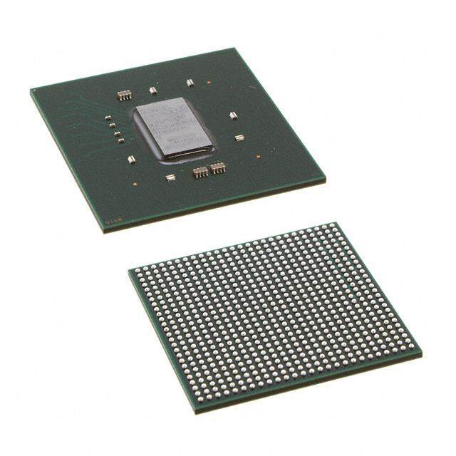
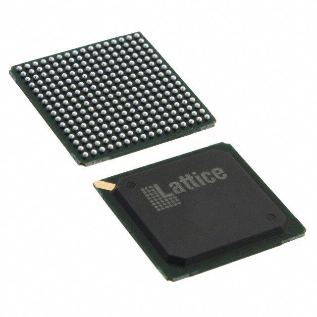
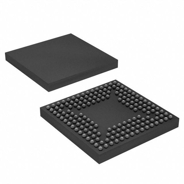
| 产品图片 |
|
| rohs | 符合RoHS无铅 / 符合限制有害物质指令(RoHS)规范要求 |
| 产品系列 | 嵌入式处理器和控制器,FPGA - 现场可编程门阵列,Lattice iCE40LP1K-CM36LP |
| 数据手册 | |
| 产品型号 | ICE40LP1K-CM36 |
| PCN组件/产地 | |
| PCN设计/规格 | |
| 产品 | iCE40 LP |
| 产品种类 | FPGA - 现场可编程门阵列 |
| 供应商器件封装 | 36-UCBGA (2.5x2.5) |
| 其它名称 | 220-1564 |
| 商标 | Lattice |
| 安装类型 | 表面贴装 |
| 安装风格 | SMD/SMT |
| 封装 | Tray |
| 封装/外壳 | 36-VFBGA |
| 封装/箱体 | CBGA-36 |
| 工作温度 | -40°C ~ 100°C |
| 工作电源电压 | 1.2 V |
| 工厂包装数量 | 490 |
| 总RAM位数 | 65536 |
| 总内存 | 64 kbit |
| 最大工作温度 | + 85 C |
| 最大工作频率 | 533 MHz |
| 最小工作温度 | - 40 C |
| 栅极数 | - |
| 栅极数量 | 1280 |
| 标准包装 | 490 |
| 电压-电源 | 1.14 V ~ 1.26 V |
| 系列 | iCE40LP1K-CM |
| 输入/输出端数量 | 25 |
| 逻辑元件/单元数 | 1280 |
| 逻辑元件数量 | 1280 |
| 逻辑数组块数量——LAB | 160 |
| 配用 | /product-detail/zh/ICE40HX1K-BLINK-EVN/220-1581-ND/3198285/product-detail/zh/ICE40LP1K-BLINK-EVN/220-1582-ND/3516591 |


- 商务部:美国ITC正式对集成电路等产品启动337调查
- 曝三星4nm工艺存在良率问题 高通将骁龙8 Gen1或转产台积电
- 太阳诱电将投资9.5亿元在常州建新厂生产MLCC 预计2023年完工
- 英特尔发布欧洲新工厂建设计划 深化IDM 2.0 战略
- 台积电先进制程称霸业界 有大客户加持明年业绩稳了
- 达到5530亿美元!SIA预计今年全球半导体销售额将创下新高
- 英特尔拟将自动驾驶子公司Mobileye上市 估值或超500亿美元
- 三星加码芯片和SET,合并消费电子和移动部门,撤换高东真等 CEO
- 三星电子宣布重大人事变动 还合并消费电子和移动部门
- 海关总署:前11个月进口集成电路产品价值2.52万亿元 增长14.8%

PDF Datasheet 数据手册内容提取
iCE40™ LP/HX Family Data Sheet DS1040 Version 3.4, October 2017
iCE40 LP/HX Family Data Sheet Introduction March 2017 Data Sheet DS1040 Features Flexible Logic Architecture — Schmitt trigger inputs, to 200 mV typical • Five devices with 384 to 7,680 LUT4s and hysteresis 10 to 206 I/Os (cid:129) Programmable pull-up mode Ultra Low Power Devices Flexible On-Chip Clocking (cid:129) Advanced 40 nm low power process (cid:129) Eight low-skew global clock resources (cid:129) As low as 21 µA standby power (cid:129) Up to two analog PLLs per device (cid:129) Programmable low swing differential I/Os Flexible Device Configuration Embedded and Distributed Memory (cid:129) SRAM is configured through: (cid:129) Up to 128 kbits sysMEM™ Embedded Block — Standard SPI Interface RAM — Internal Nonvolatile Configuration Memory Pre-Engineered Source Synchronous I/O (NVCM) (cid:129) DDR registers in I/O cells Broad Range of Package Options High Current LED Drivers (cid:129) WLCSP, QFN, VQFP, TQFP, ucBGA, caBGA, (cid:129) Three High Current Drivers used for three differ- and csBGA package options ent LEDs or one RGB LED (cid:129) Small footprint package options High Performance, Flexible I/O Buffer — As small as 1.40 mm x 1.48 mm (cid:129) Programmable sysIO™ buffer supports wide (cid:129) Advanced halogen-free packaging range of interfaces: — LVCMOS 3.3/2.5/1.8 — LVDS25E, subLVDS Table 1-1. iCE40 Family Selection Guide Part Number LP384 LP640 LP1K LP4K LP8K HX1K HX4K HX8K Logic Cells (LUT + Flip-Flop) 384 640 1,280 3,520 7,680 1,280 3,520 7,680 RAM4K Memory Blocks 0 8 16 20 32 16 20 32 RAM4K RAM bits 0 32K 64K 80K 128K 64K 80K 128K Phase-Locked Loops (PLLs) 0 0 11 22 22 11 2 2 Maximum Programmable I/O Pins 63 25 95 167 178 95 95 206 Maximum Differential Input Pairs 8 3 12 20 23 11 12 26 High Current LED Drivers 0 3 3 0 0 0 0 0 Package Code Programmable I/O: Max Inputs (LVDS25) 16 WLCSP (1.40 mm x 1.48 mm, 0.35 SWG16 10(0)1 10(0)1 mm) 32 QFN SG32 21(3) (5 mm x 5 mm, 0.5 mm) 36 ucBGA CM36 25(3) 25(3)1 (2.5 mm x 2.5 mm, 0.4 mm) 49 ucBGA CM49 37(6) 35(5)1 (3 mm x 3 mm, 0.4 mm) 81 ucBGA CM81 63(8) 63(9)2 63(9)2 (4 mm x 4 mm, 0.4 mm) 81 csBGA CB81 62(9)1 (5 mm x 5 mm, 0.5 mm) © 2017 Lattice Semiconductor Corp. All Lattice trademarks, registered trademarks, patents, and disclaimers are as listed at www.latticesemi.com/legal. All other brand or product names are trademarks or registered trademarks of their respective holders. The specifications and information herein are subject to change without notice. www.latticesemi.com 1-1 DS1040 Introduction_01.7
Introduction iCE40 LP/HX Family Data Sheet Table 1-1. iCE40 Family Selection Guide (continued) 84 QFN QN84 67(7)1 (7 mm x 7 mm, 0.5 mm) 100 VQFP VQ100 72(9)1 (14 mm x 14 mm, 0.5 mm) 121 ucBGA CM121 95(12) 93(13) 93(13) (5 mm x 5 mm, 0.4 mm) 121 csBGA CB121 92(12) (6 mm x 6 mm, 0.5 mm) 121 caBGA BG121 93(13) 93(13) (9 mm x 9 mm, 0.8 mm) 132 csBGA CB132 95(11) 95(12) 95(12) (8 mm x 8 mm, 0.5 mm) 144 TQFP TQ144 96(12) 107(14) (20 mm x 20 mm, 0.5 mm) 225 ucBGA CM225 178(23) 178(23) 178(23) (7 mm x 7 mm, 0.4 mm) 256-ball caBGA CT256 206(26) (14 mm x 14 mm, 0.8 mm) 1. No PLL available on the 16 WLCSP, 36 ucBGA, 81 csBGA, 84 QFN and 100 VQFP packages. 2. Only one PLL available on the 81 ucBGA package. 3. High Current I/Os only available on the 16 WLCSP package. Introduction The iCE40 family of ultra-low power, non-volatile FPGAs has five devices with densities ranging from 384 to 7680 Look-Up Tables (LUTs). In addition to LUT-based, low-cost programmable logic, these devices feature Embedded Block RAM (EBR), Non-volatile Configuration Memory (NVCM) and Phase Locked Loops (PLLs). These features allow the devices to be used in low-cost, high-volume consumer and system applications. Select packages offer High-Current drivers that are ideal to drive three white LEDs, or one RGB LED. The iCE40 devices are fabricated on a 40 nm CMOS low power process. The device architecture has several fea- tures such as programmable low-swing differential I/Os and the ability to turn off on-chip PLLs dynamically. These features help manage static and dynamic power consumption, resulting in low static power for all members of the family. The iCE40 devices are available in two versions – ultra low power (LP) and high performance (HX) devices. The iCE40 FPGAs are available in a broad range of advanced halogen-free packages ranging from the space saving 1.40x1.48 mm WLCSP to the PCB-friendly 20x20 mm TQFP. Table 1-1 shows the LUT densities, package and I/O options, along with other key parameters. The iCE40 devices offer enhanced I/O features such as pull-up resistors. Pull-up features are controllable on a “per-pin” basis. The iCE40 devices also provide flexible, reliable and secure configuration from on-chip NVCM. These devices can also configure themselves from external SPI Flash or be configured by an external master such as a CPU. Lattice provides a variety of design tools that allow complex designs to be efficiently implemented using the iCE40 family of devices. Popular logic synthesis tools provide synthesis library support for iCE40. Lattice design tools use the synthesis tool output along with the user-specified preferences and constraints to place and route the design in the iCE40 device. These tools extract the timing from the routing and back-annotate it into the design for timing ver- ification. Lattice provides many pre-engineered IP (Intellectual Property) modules, including a number of reference designs, licensed free of charge, optimized for the iCE40 FPGA family. By using these configurable soft core IP cores as standardized blocks, users are free to concentrate on the unique aspects of their design, increasing their productiv- ity. 1-2
iCE40 LP/HX Family Data Sheet Architecture March 2017 Data Sheet DS1040 Architecture Overview The iCE40 family architecture contains an array of Programmable Logic Blocks (PLB), sysCLOCK™ PLLs, Non- volatile Programmable Configuration Memory (NVCM) and blocks of sysMEM™ Embedded Block RAM (EBR) sur- rounded by Programmable I/O (PIO). Figure 2-1 shows the block diagram of the iCE40LP/HX1K device. Figure 2-1. iCE40LP/HX1K Device, Top View Programmable Logic Block (PLB) I/O Bank 0 Programmable Interconnect ck o LB LB M LB LB LB LB LB LB c Bl ct P P A P P P P P P ct gi ank 3 e Interconne PLB PLB 4 kbit R PLB PLB PLB PLB PLB PLB e Interconne ank 1 ammable Lo I/O B ogrammabl PLB PLB bit RAM PLB PLB PLB PLB PLB PLB ogrammabl I/O B ells = Progr Pr PLB PLB 4 k PLB PLB PLB PLB PLB PLB Pr gic C o NVCM PLL 8 L SPI I/O Bank 2 Bank Non-volatile Phase-Locked Carry Logic Configuration Memory Loop (NVCM) 4-Input Look-up Table (LUT4) Flip-flop with Enable and Reset Controls The logic blocks, Programmable Logic Blocks (PLB) and sysMEM EBR blocks, are arranged in a two-dimensional grid with rows and columns. Each column has either logic blocks or EBR blocks. The PIO cells are located at the periphery of the device, arranged in banks. The PLB contains the building blocks for logic, arithmetic, and register functions. The PIOs utilize a flexible I/O buffer referred to as a sysIO buffer that supports operation with a variety of interface standards. The blocks are connected with many vertical and horizontal routing channel resources. The place and route software tool automatically allocates these routing resources. In the iCE40 family, there are up to four independent sysIO banks. Note on some packages V banks are tied CCIO together. There are different types of I/O buffers on the different banks. Refer to the details in later sections of this document. The sysMEM EBRs are large 4 kbit, dedicated fast memory blocks. These blocks can be configured as RAM, ROM or FIFO. The iCE40 architecture also provides up to two sysCLOCK Phase Locked Loop (PLL) blocks. The PLLs have mul- tiply, divide, and phase shifting capabilities that are used to manage the frequency and phase relationships of the clocks. Every device in the family has a SPI port that supports programming and configuration of the device. The iCE40 includes on-chip, Nonvolatile Configuration Memory (NVCM). © 2017 Lattice Semiconductor Corp. All Lattice trademarks, registered trademarks, patents, and disclaimers are as listed at www.latticesemi.com/legal. All other brand or product names are trademarks or registered trademarks of their respective holders. The specifications and information herein are subject to change without notice. www.latticesemi.com 2-1 DS1040 Architecture_01.4
Architecture iCE40 LP/HX Family Data Sheet PLB Blocks The core of the iCE40 device consists of Programmable Logic Blocks (PLB) which can be programmed to perform logic and arithmetic functions. Each PLB consists of eight interconnected Logic Cells (LC) as shown in Figure 2-2. Each LC contains one LUT and one register. Figure 2-2. PLB Block Diagram Shared Block-Level Controls Programmable Logic Clock Block (PLB) Enable FCOUT 1 Set/Reset 0 Logic Cell Carry Logic DFF O I0 D Q s) I1 EN C L LUT4 SR s ( I2 ell I3 C c gi o L 8 FCIN Four-input Flip-flop with Look-Up Table optional enable and (LUT4) set or reset controls = Statically defined by configuration program Logic Cells Each Logic Cell includes three primary logic elements shown in Figure 2-2. (cid:129) A four-input Look-Up Table (LUT4) builds any combinational logic function, of any complexity, requiring up to four inputs. Similarly, the LUT4 element behaves as a 16x1 Read-Only Memory (ROM). Combine and cas- cade multiple LUT4s to create wider logic functions. (cid:129) A ‘D’-style Flip-Flop (DFF), with an optional clock-enable and reset control input, builds sequential logic func- tions. Each DFF also connects to a global reset signal that is automatically asserted immediately following device configuration. (cid:129) Carry Logic boosts the logic efficiency and performance of arithmetic functions, including adders, subtractors, comparators, binary counters and some wide, cascaded logic functions. Table 2-1. Logic Cell Signal Descriptions Function Type Signal Names Description Input Data signal I0, I1, I2, I3 Inputs to LUT4 Input Control signal Enable Clock enable shared by all LCs in the PLB Asynchronous or synchronous local set/reset shared by all LCs in Input Control signal Set/Reset1 the PLB. Clock one of the eight Global Buffers, or from the general-purpose Input Control signal Clock interconnects fabric shared by all LCs in the PLB Input Inter-PLB signal FCIN Fast carry in Output Data signals O LUT4 or registered output Output Inter-PFU signal FCOUT Fast carry out 1. If Set/Reset is not used, then the flip-flop is never set/reset, except when cleared immediately after configuration. 2-2
Architecture iCE40 LP/HX Family Data Sheet Routing There are many resources provided in the iCE40 devices to route signals individually with related control signals. The routing resources consist of switching circuitry, buffers and metal interconnect (routing) segments. The inter-PLB connections are made with three different types of routing resources: Adjacent (spans two PLBs), x4 (spans five PLBs) and x12 (spans thirteen PLBs). The Adjacent, x4 and x12 connections provide fast and efficient connections in the diagonal, horizontal and vertical directions. The design tool takes the output of the synthesis tool and places and routes the design. Clock/Control Distribution Network Each iCE40 device has eight global inputs, two pins on each side of the device. Note that not all GBINs are avail- able in all packages. These global inputs can be used as high fanout nets, clock, reset or enable signals. The dedicated global pins are identified as GBIN[7:0] and the global buffers are identified as-GBUF[7:0]. These eight inputs may be used as gen- eral purpose I/O if they are not used to drive the clock nets. Global buffer GBUF7 in I/O Bank 3 also provides an optional direct LVDS25 or subLVDS differential clock input. Table 2-2 lists the connections between a specific global buffer and the inputs on a PLB. All global buffers optionally connect to the PLB CLK input. Any four of the eight global buffers can drive logic inputs to a PLB. Even-numbered global buffers optionally drive the Set/Reset input to a PLB. Similarly, odd-numbered buffers optionally drive the PLB clock-enable input. Table 2-2. Global Buffer (GBUF) Connections to Programmable Logic Blocks Global Buffer LUT Inputs Clock Reset Clock Enable GBUF0 Yes Yes GBUF1 Yes Yes GBUF2 Yes Yes GBUF3 Yes, any 4 of 8 Yes Yes GBUF4 GBUF Inputs Yes Yes GBUF5 Yes Yes GBUF6 Yes Yes GBUF7 Yes Yes The maximum frequency for the global buffers are shown in the iCE40 External Switching Characteristics tables later in this document. Global Hi-Z Control The global high-impedance control signal, GHIZ, connects to all I/O pins on the iCE40 device. This GHIZ signal is automatically asserted throughout the configuration process, forcing all user I/O pins into their high-impedance state. 2-3
Architecture iCE40 LP/HX Family Data Sheet Global Reset Control The global reset control signal connects to all PLB and PIO flip-flops on the iCE40 device. The global reset signal is automatically asserted throughout the configuration process, forcing all flip-flops to their defined wake-up state. For PLB flip-flops, the wake-up state is always reset, regardless of the PLB flip-flop primitive used in the application. sysCLOCK Phase Locked Loops (PLLs) The sysCLOCK PLLs provide the ability to synthesize clock frequencies. The iCE40 devices have one or more sys- CLOCK PLLs. REFERENCECLK is the reference frequency input to the PLL and its source can come from an external I/O pin or from internal routing. EXTFEEDBACK is the feedback signal to the PLL which can come from internal routing or an external I/O pin. The feedback divider is used to multiply the reference frequency and thus synthesize a higher frequency clock output. The PLLOUT output has an output divider, thus allowing the PLL to generate different frequencies for each output. The output divider can have a value from 1 to 6. The PLLOUT outputs can all be used to drive the iCE40 global clock network directly or general purpose routing resources can be used. The LOCK signal is asserted when the PLL determines it has achieved lock and de-asserted if a loss of lock is detected. A block diagram of the PLL is shown in Figure 2-3. The timing of the device registers can be optimized by programming a phase shift into the PLLOUT output clock which will advance or delay the output clock with reference to the REFERENCECLK clock. This phase shift can be either programmed during configuration or can be adjusted dynamically. In dynamic mode, the PLL may lose lock after a phase adjustment on the output used as the feedback source and not relock until the t parameter has LOCK been satisfied. For more details on the PLL, see TN1251, iCE40 sysCLOCK PLL Design and Usage Guide. Figure 2-3. PLL Diagram RESET BYPASS BYPASS GNDPLL VCCPLL Phase DIVR Detector RANGE DIVQ REFERENCECLK Voltage Input Low-Pass Controlled VCO Divider Filter Oscillator Divider (VCO) SIMPLE DIVF PLLOUTCORE FeDeivdibdaecrk Fine Delay AFdinjues Dtmeelanyt SPhhiaftseer OAdujtupsuttm Peonrtt PLLOUTGLOBAL Feedback Feedback_Path LOCK DYNAMICDELAY[7:0] EXTFEEDBACK EXTERNAL LATCHINPUTVALUE Low Power mode (iCEgate enabled) Table 2-3 provides signal descriptions of the PLL block. 2-4
Architecture iCE40 LP/HX Family Data Sheet Table 2-3. PLL Signal Descriptions Signal Name Direction Description REFERENCECLK Input Input reference clock When FEEDBACK_PATH is set to SIMPLE, the BYPASS control selects which clock sig- nal connects to the PLLOUT output. BYPASS Input 0 = PLL generated signal 1 = REFERENCECLK External feedback input to PLL. Enabled when the FEEDBACK_PATH attribute is set to EXTFEEDBACK Input EXTERNAL. Fine delay adjustment control inputs. Enabled when DELAY_ADJUSTMENT_MODE is DYNAMICDELAY[3:0] Input set to DYNAMIC. When enabled, forces the PLL into low-power mode; PLL output is held static at the last LATCHINPUTVALUE Input input clock value. Set ENABLE ICEGATE_PORTA and PORTB to ‘1’ to enable. Output from the Phase-Locked Loop (PLL). Drives a global clock network on the FPGA. PLLOUTGLOBAL Output The port has optimal connections to global clock buffers GBUF4 and GBUF5. Output clock generated by the PLL, drives regular FPGA routing. The frequency gener- PLLOUTCORE Output ated on this output is the same as the frequency of the clock signal generated on the PLLOUTLGOBAL port. When High, indicates that the PLL output is phase aligned or locked to the input refer- LOCK Output ence clock. RESET Input Active low reset. sysMEM Embedded Block RAM Memory Larger iCE40 device includes multiple high-speed synchronous sysMEM Embedded Block RAMs (EBRs), each 4 kbit in size. This memory can be used for a wide variety of purposes including data buffering, and FIFO. sysMEM Memory Block The sysMEM block can implement single port, pseudo dual port, or FIFO memories with programmable logic resources. Each block can be used in a variety of depths and widths as shown in Table 2-4. Table 2-4. sysMEM Block Configurations1 Block RAM Block RAM Configuration WADDR Port WDATA Port RADDR Port RDATA Port MASK Port Configuration and Size Size (Bits) Size (Bits) Size (Bits) Size (Bits) Size (Bits) SB_RAM256x16 SB_RAM256x16NR 256x16 (4K) 8 [7:0] 16 [15:0] 8 [7:0] 16 [15:0] 16 [15:0] SB_RAM256x16NW SB_RAM256x16NRNW SB_RAM512x8 SB_RAM512x8NR 512x8 (4K) 9 [8:0] 8 [7:0] 9 [8:0] 8 [7:0] No Mask Port SB_RAM512x8NW SB_RAM512x8NRNW SB_RAM1024x4 SB_RAM1024x4NR 1024x4 (4K) 10 [9:0] 4 [3:0] 10 [9:0] 4 [3:0] No Mask Port SB_RAM1024x4NW SB_RAM1024x4NRNW SB_RAM2048x2 SB_RAM2048x2NR 2048x2 (4K) 11 [10:0] 2 [1:0] 11 [10:0] 2 [1:0] No Mask Port SB_RAM2048x2NW SB_RAM2048x2NRNW 1. For iCE40 EBR primitives with a negative-edged Read or Write clock, the base primitive name is appended with a ‘N’ and a ‘R’ or ‘W’ depending on the clock that is affected. 2-5
Architecture iCE40 LP/HX Family Data Sheet RAM Initialization and ROM Operation If desired, the contents of the RAM can be pre-loaded during device configuration. By preloading the RAM block during the chip configuration cycle and disabling the write controls, the sysMEM block can also be utilized as a ROM. Note the sysMEM Embedded Block RAM Memory address 0 cannot be initialized. Memory Cascading Larger and deeper blocks of RAM can be created using multiple EBR sysMEM Blocks. RAM4k Block Figure 2-4 shows the 256x16 memory configurations and their input/output names. In all the sysMEM RAM modes, the input data and addresses for the ports are registered at the input of the memory array. Figure 2-4. sysMEM Memory Primitives Write Port Read Port WDATA[15:0] RDATA[15:0] MASK[15:0] WADDR[7:0] RADDR[7:0] RAM4K RAM Block WE (256x16) RE WCLKE RCLKE WCLK RCLK Table 2-5. EBR Signal Descriptions Signal Name Direction Description WDATA[15:0] Input Write Data input. Masks write operations for individual data bit-lines. MASK[15:0] Input 0 = write bit; 1 = don’t write bit WADDR[7:0] Input Write Address input. Selects one of 256 possible RAM locations. WE Input Write Enable input. WCLKE Input Write Clock Enable input. WCLK Input Write Clock input. Default rising-edge, but with falling-edge option. RDATA[15:0] Output Read Data output. RADDR[7:0] Input Read Address input. Selects one of 256 possible RAM locations. RE Input Read Enable input. RCLKE Input Read Clock Enable input. RCLK Input Read Clock input. Default rising-edge, but with falling-edge option. For further information on the sysMEM EBR block, please refer to TN1250, Memory Usage Guide for iCE40 De- vices. 2-6
Architecture iCE40 LP/HX Family Data Sheet sysIO Buffer Banks iCE40 devices have up to four I/O banks with independent V rails with an additional configuration bank CCIO V for the SPI I/Os. CC_SPI Programmable I/O (PIO) The programmable logic associated with an I/O is called a PIO. The individual PIO are connected to their respec- tive sysIO buffers and pads. The PIOs are placed on all four sides of the device. Figure 2-5. I/O Bank and Programmable I/O Cell VCCIO I/O Bank 0, 1, 2, or 3 Voltage Supply 0 = Hi-Z Enabled ‘1’ 1 = Output Disabled ‘0’ Enabled Pull-up OE VCC VCCIO_0 Pull-up Internal Core Enable OUTCLK I/O Bank 0 General-Purpose I/O OUT PIO PAD O VCCIO_3 I/O Bank 3ecial/LVDS I/O I/O Bank 1eral-Purpose I/ IVCCIO_1NIN iCHEOOGULATDTCELK HD Lslowawtictechsh tii nnphgoi wbfoietrsr p n S e G GBIN pins optionally I/O Bank 2 SPI INCLK connect directly to an associated GBUF global General-Purpose I/O Bank buffer Programmable Input/Output VCC_SPI VCCIO_2 = Statically defined by configuration program The PIO contains three blocks: an input register block, output register block iCEgate™ and tri-state register block. To save power, the optional iCEgateTM latch can selectively freeze the state of individual, non-registered inputs within an I/O bank. Note that the freeze signal is common to the bank. These blocks can operate in a variety of modes along with the necessary clock and selection logic. Input Register Block The input register blocks for the PIOs on all edges contain registers that can be used to condition high-speed inter- face signals before they are passed to the device core. In Generic DDR mode, two registers are used to sample the data on the positive and negative edges of the system clock signal, creating two data streams. Output Register Block The output register block can optionally register signals from the core of the device before they are passed to the sysIO buffers. In Generic DDR mode, two registers are used to capture the data on the positive and negative edge of the system clock and then muxed creating one data stream. Figure 2-6 shows the input/output register block for the PIOs. 2-7
Architecture iCE40 LP/HX Family Data Sheet Figure 2-6. iCE I/O Register Block Diagram CLOCK_ENABLE PIO Pair OUTPUT_CLK INPUT_CLK (1,0) LATCH_INPUT_VALUE D_IN_1 D_IN_0 Pad D_OUT_1 D_OUT_0 (1,0) 0 1 OUTPUT_ENABLE (1,0) LATCH_INPUT_VALUE D_IN_1 D_IN_0 Pad D_OUT_1 D_OUT_0 (1,0) 0 1 OUTPUT_ENABLE = Statically defined by configuration program. Table 2-6. PIO Signal List Pin Name I/O Type Description OUTPUT_CLK Input Output register clock CLOCK_ENABLE Input Clock enable INPUT_CLK Input Input register clock OUTPUT_ENABLE Input Output enable D_OUT_0/1 Input Data from the core D_IN_0/1 Output Data to the core LATCH_INPUT_VALUE Input Latches/holds the Input Value sysIO Buffer Each I/O is associated with a flexible buffer referred to as a sysIO buffer. These buffers are arranged around the periphery of the device in groups referred to as banks. The sysIO buffers allow users to implement a wide variety of standards that are found in today’s systems including LVCMOS and LVDS25. High Current LED Drivers combine three sysIO buffers together. This allows for programmable drive strength. This also allows for high current drivers that are ideal to drive three white LEDs, or one RGB LED. Each bank is capable of supporting multiple I/O standards including single-ended LVCMOS buffers and differential LVDS25E output buf- 2-8
Architecture iCE40 LP/HX Family Data Sheet fers. Bank 3 additionally supports differential LVDS25 input buffers. Each sysIO bank has its own dedicated power supply. Typical I/O Behavior During Power-up The internal power-on-reset (POR) signal is deactivated when V , V , V , and V have reached CC CCIO_2 PP_2V5 CC_SPI the level defined in the Power-On-Reset Voltage table in the DC and Switching Characteristics section of this data sheet. After the POR signal is deactivated, the FPGA core logic becomes active. It is the user’s responsibility to ensure that all V banks are active with valid input logic levels to properly control the output logic states of all CCIO the I/O banks that are critical to the application. The default configuration of the I/O pins in a device prior to config- uration is tri-stated with a weak pull-up to V . The I/O pins will maintain the pre-configuration state until V and CCIO CC V (for I/O banks containing configuration I/Os) have reached levels, at which time the I/Os will take on the soft- CCIO ware user-configured settings only after a proper download/configuration. Unused IOs are automatically blocked and the pullup termination is disabled. Supported Standards The iCE40 sysIO buffer supports both single-ended and differential input standards. The single-ended standard supported is LVCMOS. The buffer supports the LVCMOS 1.8, 2.5, and 3.3 V standards. The buffer has individually configurable options for bus maintenance (weak pull-up or none). The High Current output buffer have individually configurable options for drive strength. Table 2-7 and Table 2-8 show the I/O standards (together with their supply and reference voltages) supported by the iCE40 devices. Table 2-7. Supported Input Standards V (Typical) CCIO Input Standard 3.3 V 2.5 V 1.8 V Single-Ended Interfaces LVCMOS33 Yes LVCMOS25 Yes LVCMOS18 Yes Differential Interfaces LVDS251 Yes subLVDS1 Yes 1. Bank 3 only. Table 2-8. Supported Output Standards Output Standard V (Typical) CCIO Single-Ended Interfaces LVCMOS33 3.3 LVCMOS25 2.5 LVCMOS18 1.8 Differential Interfaces LVDS25E1 2.5 subLVDSE1 1.8 1. These interfaces can be emulated with external resistors in all devices. Non-Volatile Configuration Memory All iCE40 devices provide a Non-Volatile Configuration Memory (NVCM) block which can be used to configure the device. For more information on the NVCM, please refer to TN1248, iCE40 Programming and Configuration Usage Guide. 2-9
Architecture iCE40 LP/HX Family Data Sheet Power On Reset iCE40 devices have power-on reset circuitry to monitor V , V , V , and V voltage levels during CC CCIO_2 PP_2V5 CC_SPI power-up and operation. At power-up, the POR circuitry monitors V , V , V , and V (controls CC CCIO_2 PP_2V5 CC_SPI configuration) voltage levels. It then triggers download from the on-chip NVCM or external Flash memory after reaching the power-up levels specified in the Power-On-Reset Voltage table in the DC and Switching Characteris- tics section of this data sheet. Before and during configuration, the I/Os are held in tri-state. I/Os are released to user functionality once the device has finished configuration. Programming and Configuration This section describes the programming and configuration of the iCE40 family. Device Programming The NVCM memory can be programmed through the SPI port. Device Configuration There are various ways to configure the Configuration RAM (CRAM) including: 1. Internal NVCM Download 2. From a SPI Flash (Master SPI mode) 3. System microprocessor to drive a Serial Slave SPI port (SSPI mode) The image to configure the CRAM can be selected by the user on power up (Cold Boot) or once powered up (Warm Boot). For more details on programming and configuration, see TN1248, iCE40 Programming and Configuration Usage Guide. Power Saving Options iCE40 devices are available in two options for maximum flexibility: LP and HX devices. The LP devices have ultra low static and dynamic power consumption. HX devices are designed to provide high performance. Both the LP and the HX devices operate at 1.2 V V . CC iCE40 devices feature iCEGate and PLL low power mode to allow users to meet the static and dynamic power requirements of their applications. While these features are available in both device types, these features are mainly intended for use with iCE40 LP devices to manage power consumption. Table 2-9. iCE40 Power Saving Features Description Device Subsystem Feature Description When LATCHINPUTVALUE is enabled, forces the PLL into low-power mode; PLL output held static PLL at last input clock value. To save power, the optional iCEgate latch can selectively freeze the state of individual, non-regis- iCEGate tered inputs within an I/O bank. Registered inputs are effectively frozen by their associated clock or clock-enable control. 2-10
iCE40 LP/HX Family Data Sheet DC and Switching Characteristics October 2015 Data Sheet DS1040 Absolute Maximum Ratings1, 2, 3, 4 iCE40 LP/HX Supply Voltage V . . . . . . . . . . . . . . . . . . . . . . . . . . . . . . . . . . . . . . . . . . . . . . . . . . . . . . . . . . –0.5 V to 1.42 V CC Output Supply Voltage V V . . . . . . . . . . . . . . . . . . . . . . . . . . . . . . . . . . . . . . . . . . . –0.5 V to 3.60 V CCIO, CC_SPI NVCM Supply Voltage V . . . . . . . . . . . . . . . . . . . . . . . . . . . . . . . . . . . . . . . . . . . . . . . . . –0.5 V to 3.60 V PP_2V5 PLL Supply Voltage V . . . . . . . . . . . . . . . . . . . . . . . . . . . . . . . . . . . . . . . . . . . . . . . . . . . . –0.5 V to 1.30 V CCPLL I/O Tri-state Voltage Applied. . . . . . . . . . . . . . . . . . . . . . . . . . . . . . . . . . . . . . . . . . . . . . . . . . . . –0.5 V to 3.60 V Dedicated Input Voltage Applied . . . . . . . . . . . . . . . . . . . . . . . . . . . . . . . . . . . . . . . . . . . . . . . . –0.5 V to 3.60 V Storage Temperature (Ambient). . . . . . . . . . . . . . . . . . . . . . . . . . . . . . . . . . . . . . . . . . . . . . . . .–65 °C to 150 °C Junction Temperature (T ) . . . . . . . . . . . . . . . . . . . . . . . . . . . . . . . . . . . . . . . . . . . . . . . . . . . . .–55 °C to 125 °C J 1. Stress above those listed under the “Absolute Maximum Ratings” may cause permanent damage to the device. Functional operation of the device at these or any other conditions above those indicated in the operational sections of this specification is not implied. 2. Compliance with the Lattice Thermal Management document is required. 3. All voltages referenced to GND. 4. IOs can support a 200 mV Overshoot above the Recommend Operating Conditions V (Max) and -200mV Undershoot below V (Min). CCIO IL Overshoot and Undershoot is permitted for 25% duty cycle but must not exceed 1.6 ns. Recommended Operating Conditions1 Symbol Parameter Min. Max. Units V 1 Core Supply Voltage 1.14 1.26 V CC Slave SPI Configuration 1.71 3.46 V V NVCM Programming and Master SPI Configuration 2.30 3.46 V V PP_2V5 PP_2V5 Operating Supply Voltage Configure from NVCM 2.30 3.46 V NVCM Programming 2.30 3.00 V V 4 Optional fast NVCM programming supply. Leave unconnected. N/A N/A V PP_FAST V 5, 6 PLL Supply Voltage 1.14 1.26 V CCPLL V 1.71 3.46 V V 1, 2, 3 I/O Driver Supply Voltage CCIO0-3 CCIO V 1.71 3.46 V CC_SPI t Junction Temperature Industrial Operation –40 100 °C JIND t Junction Temperature NVCM Programming 10 30 °C PROG 1. Like power supplies must be tied together. For example, if V and V are both the same voltage, they must also be the same sup- CCIO CC_SPI ply. 2. See recommended voltages by I/O standard in subsequent table. 3. V pins of unused I/O banks should be connected to the V power supply on boards. CCIO CC 4. V , used only for fast production programming, must be left floating or unconnected in applications, except CM36 and CM49 pack- PP_FAST ages MUST have the V ball connected to V ball externally. PP_FAST CCIO_0 5. No PLL available on the iCE40LP384 and iCE40LP640 device. 6. V is tied to V internally in packages without PLLs pins. CCPLL CC © 2015 Lattice Semiconductor Corp. All Lattice trademarks, registered trademarks, patents, and disclaimers are as listed at www.latticesemi.com/legal. All other brand or product names are trademarks or registered trademarks of their respective holders. The specifications and information herein are subject to change without notice. www.latticesemi.com 3-1 DS1040 DC and Switching_02.0
DC and Switching Characteristics iCE40 LP/HX Family Data Sheet Power Supply Ramp Rates1, 2 Symbol Parameter Min. Max. Units All configuration modes. No power 0.40 10 V/ms supply sequencing. Configuring from Slave SPI. No 0.01 10 V/ms power supply sequencing, tRAMP Power spuopwpelyr rsaumppp lireaste.s for all CVonfigur itnog b fero pmo wNeVrCedM 0. .V2C5 Cm asn d 0.01 10 V/ms PP_2V5 before V . CC_SPI Configuring from MSPI. V and 0.01 10 V/ms CC V to be powered 0.25 ms PP_SPI before V . PP_2V5 1. Assumes monotonic ramp rates. 2. iCE40LP384 requires V to be greater than 0.7V when V and V are above GND. CC CCIO CC_SPI Power-On-Reset Voltage Levels1 Symbol Device Parameter Min. Max. Units V iCE40LP384 Power-On-Reset ramp-up trip point VCC 0.67 0.99 V PORUP (band gap based circuit monitoring VCCIO_2 0.70 1.59 V VCC, VCCIO_2, VCC_SPI and VPP_2V5) VCC_SPI 0.70 1.59 V VPP_2V5 0.70 1.59 V iCE40LP640, Power-On-Reset ramp-up trip point VCC 0.55 0.75 V iCE40LP/HX1K, (band gap based circuit monitoring VCCIO_2 0.86 1.29 V iCE40LP/HX4K, VCC, VCCIO_2, VCC_SPI and iCE40LP/HX8K VPP_2V5) VCC_SPI 0.86 1.29 V VPP_2V5 0.86 1.33 V V iCE40LP384 Power-On-Reset ramp-down trip VCC — 0.64 V PORDN point (band gap based circuit moni- VCCIO_2 — 1.59 V toring VCC, VCCIO_2, VCC_SPI and VPP_2V5) VCC_SPI — 1.59 V VPP_2V5 — 1.59 V iCE40LP640, Power-On-Reset ramp-down trip VCC — 0.75 V iCE40LP/HX1K, point (band gap based circuit moni- VCCIO_2 — 1.29 V iCE40LP/HX4K, toring VCC, VCCIO_2, VCC_SPI iCE40LP/HX8K and VPP_2V5) VCC_SPI — 1.29 V VPP_2V5 — 1.33 V 1. These POR trip points are only provided for guidance. Device operation is only characterized for power supply voltages specified under rec- ommended operating conditions. ESD Performance Please refer to the iCE40 Product Family Qualification Summary for complete qualification data, including ESD per- formance. 3-2
DC and Switching Characteristics iCE40 LP/HX Family Data Sheet DC Electrical Characteristics Over Recommended Operating Conditions Symbol Parameter Condition Min. Typ. Max. Units I I 1, 3, 4, 5, 6, 7 Input or I/O Leakage 0V < V < V + 0.2 V — — +/–10 µA IL, IH IN CCIO C 6, 7 V = 3.3 V, 2.5 V, 1.8 V 1 I/O Capacitance2 CCIO — 6 — pf V = Typ., V = 0 to V + 0.2 V CC IO CCIO C 6, 7 Global Input Buffer V = 3.3 V, 2.5 V, 1.8 V 2 CCIO — 6 — pf Capacitance2 V = Typ., V = 0 to V + 0.2 V CC IO CCIO V Input Hysteresis V = 1.8 V, 2.5 V, 3.3 V — 200 — mV HYST CCIO I 6, 7 Internal PIO Pull-up V = 1.8 V, 0=<V <=0.65 V –3 — –31 µA PU CCIO IN CCIO Current V = 2.5 V, 0=<V <=0.65 V –8 — –72 µA CCIO IN CCIO V = 3.3 V, 0=<V <=0.65 V –11 — –128 µA CCIO IN CCIO 1. Input or I/O leakage current is measured with the pin configured as an input or as an I/O with the output driver tri-stated. It is not measured with the output driver active. Internal pull-up resistors are disabled. 2. T 25°C, f = 1.0 MHz. J 3. Please refer to V and V in the sysIO Single-Ended DC Electrical Characteristics table of this document. IL IH 4. Only applies to IOs in the SPI bank following configuration. 5. Some products are clamped to a diode when V is larger than V . IN CCIO 6. High current IOs has three sysIO buffers connected together. 7. The iCE40LP640 and iCE40LP1K SWG16 package has CDONE and a sysIO buffer are connected together. Static Supply Current – LP Devices1, 2, 3, 4 Symbol Parameter Device Typ. V 4 Units CC iCE40LP384 21 µA iCE40LP640 100 µA I Core Power Supply iCE40LP1K 100 µA CC iCE40LP4K 250 µA iCE40LP8K 250 µA I 5, 6 PLL Power Supply All devices 0.5 µA CCPLL I NVCM Power Supply All devices 1.0 µA PP_2V5 Bank Power Supply4 I I All devices 3.5 µA CCIO, CC_SPI V = 2.5 V CCIO 1. Assumes blank pattern with the following characteristics: all outputs are tri-stated, all inputs are configured as LVCMOS and held at V CCIO or GND, on-chip PLL is off. For more detail with your specific design, use the Power Calculator tool. Power specified with master SPI con- figuration mode. Other modes may be up to 25% higher. 2. Frequency = 0 MHz. 3. T = 25 °C, power supplies at nominal voltage. J 4. Does not include pull-up. 5. No PLL available on the iCE40LP384 and iCE40LP640 device. 6. V is tied to V internally in packages without PLLs pins. CCPLL CC 3-3
DC and Switching Characteristics iCE40 LP/HX Family Data Sheet Static Supply Current – HX Devices1, 2, 3, 4 Symbol Parameter Device Typ. V 4 Units CC iCE40HX1K 296 µA I Core Power Supply iCE40HX4K 1140 µA CC iCE40HX8K 1140 µA I 5 PLL Power Supply All devices 0.5 µA CCPLL I NVCM Power Supply All devices 1.0 µA PP_2V5 Bank Power Supply4 I I All devices 3.5 µA CCIO, CC_SPI V = 2.5 V CCIO 1. Assumes blank pattern with the following characteristics: all outputs are tri-stated, all inputs are configured as LVCMOS and held at V CCIO or GND, on-chip PLL is off. For more detail with your specific design, use the Power Calculator tool. Power specified with master SPI config- uration mode. Other modes may be up to 25% higher. 2. Frequency = 0 MHz. 3. T = 25 °C, power supplies at nominal voltage. J 4. Does not include pull-up. 5. V is tied to V internally in packages without PLLs pins. CCPLL CC Programming NVCM Supply Current – LP Devices1, 2, 3, 4 Symbol Parameter Device Typ. V 5 Units CC iCE40LP384 60 µA iCE40LP640 120 µA I Core Power Supply iCE40LP1K 120 µA CC iCE40LP4K 350 µA iCE40LP8K 350 µA I 6, 7 PLL Power Supply All devices 0.5 µA CCPLL I NVCM Power Supply All devices 2.5 mA PP_2V5 I 8 I Bank Power Supply5 All devices 3.5 mA CCIO, CC_SPI 1. Assumes all inputs are held at V or GND and all outputs are tri-stated. CCIO 2. Typical user pattern. 3. SPI programming is at 8 MHz. 4. T = 25 °C, power supplies at nominal voltage. J 5. Per bank. V = 2.5 V. Does not include pull-up. CCIO 6. No PLL available on the iCE40-LP384 and iCE40-LP640 device. 7. V is tied to V internally in packages without PLLs pins. CCPLL CC 8. V , used only for fast production programming, must be left floating or unconnected in applications, except CM36 and CM49 pack- PP_FAST ages MUST have the V ball connected to V ball externally. PP_FAST CCIO_0 3-4
DC and Switching Characteristics iCE40 LP/HX Family Data Sheet Programming NVCM Supply Current – HX Devices1, 2, 3, 4 Symbol Parameter Device Typ. V 5 Units CC iCE40HX1K 278 µA I Core Power Supply iCE40HX4K 1174 µA CC iCE40HX8K 1174 µA I 6 PLL Power Supply All devices 0.5 µA CCPLL I NVCM Power Supply All devices 2.5 mA PP_2V5 I 7 I Bank Power Supply5 All devices 3.5 mA CCIO, CC_SPI 1. Assumes all inputs are held at V or GND and all outputs are tri-stated. CCIO 2. Typical user pattern. 3. SPI programming is at 8 MHz. 4. T = 25 °C, power supplies at nominal voltage. J 5. Per bank. V = 2.5 V. Does not include pull-up. CCIO 6. V is tied to V internally in packages without PLLs pins. CCPLL CC 7. V , used only for fast production programming, must be left floating or unconnected in applications. PP_FAST Peak Startup Supply Current – LP Devices Symbol Parameter Device Max Units iCE40LP384 7.7 mA iCELP640 6.4 mA I Core Power Supply iCE40LP1K 6.4 mA CCPEAK iCE40LP4K 15.7 mA iCE40LP8K 15.7 mA iCE40LP1K 1.5 mA iCELP640 1.5 mA I 1, 2, 4 PLL Power Supply CCPLLPEAK iCE40LP4K 8.0 mA iCE40LP8K 8.0 mA iCE40LP384 3.0 mA iCELP640 7.7 mA I NVCM Power Supply iCE40LP1K 7.7 mA PP_2V5PEAK iCE40LP4K 4.2 mA iCE40LP8K 4.2 mA iCE40LP384 5.7 mA I 3 NVCM Programming Supply iCELP640 8.1 mA PP_FASTPEAK iCE40LP1K 8.1 mA iCE40LP384 8.4 mA iCELP640 3.3 mA I 5, I Bank Power Supply iCE40LP1K 3.3 mA CCIOPEAK CC_SPIPEAK iCE40LP4K 8.2 mA iCE40LP8K 8.2 mA 1. No PLL available on the iCE40LP384 and iCE40LP640 device. 2. V is tied to V internally in packages without PLLs pins. CCPLL CC 3. V , used only for fast production programming, must be left floating or unconnected in applications, except CM36 and CM49 pack- PP_FAST ages MUST have the V ball connected to V ball externally. PP_FAST CCIO_0 4. While no PLL is available in the iCE40-LP640 the I is additive to I . CCPLLPEAK CCPEAK 5. iCE40LP384 requires V to be greater than 0.7 V when V and V are above GND. CC CCIO CC_SPI 3-5
DC and Switching Characteristics iCE40 LP/HX Family Data Sheet Peak Startup Supply Current – HX Devices Symbol Parameter Device Max Units iCE40HX1K 6.9 mA I Core Power Supply iCE40HX4K 22.3 mA CCPEAK iCE40HX8K 22.3 mA iCE40HX1K 1.8 mA I 1 PLL Power Supply iCE40HX4K 6.4 mA CCPLLPEAK iCE40HX8K 6.4 mA iCE40HX1K 2.8 mA I NVCM Power Supply iCE40HX4K 4.1 mA PP_2V5PEAK iCE40HX8K 4.1 mA iCE40HX1K 6.8 mA I , I Bank Power Supply iCE40HX4K 6.8 mA CCIOPEAK CC_SPIPEAK iCE40HX8K 6.8 mA 1. V is tied to V internally in packages without PLLs pins. CCPLL CC sysIO Recommended Operating Conditions V (V) CCIO Standard Min. Typ. Max. LVCMOS 3.3 3.14 3.3 3.46 LVCMOS 2.5 2.37 2.5 2.62 LVCMOS 1.8 1.71 1.8 1.89 LVDS25E1, 2 2.37 2.5 2.62 subLVDSE1, 2 1.71 1.8 1.89 1. Inputs on-chip. Outputs are implemented with the addition of external resistors. 2. Does not apply to Configuration Bank V . CC_SPI sysIO Single-Ended DC Electrical Characteristics Input/ V V 1 IL IH Output V Max. V Min. I Max. OL OH OL Standard Min. (V) Max. (V) Min. (V) Max. (V) (V) (V) (mA) I Max. (mA) OH 0.4 V – 0.4 8, 162, 242 –8, –162, –242 LVCMOS 3.3 –0.3 0.8 2.0 V + 0.2 V CCIO CCIO 0.2 V – 0.2 0.1 –0.1 CCIO 0.4 V – 0.4 6, 122, 182 –6, –122, –182 LVCMOS 2.5 –0.3 0.7 1.7 V + 0.2 V CCIO CCIO 0.2 V – 0.2 0.1 –0.1 CCIO 0.4 V – 0.4 4, 82, 122 –4, –82, –122 LVCMOS 1.8 –0.3 0.35V 0.65V V + 0.2 V CCIO CCIO CCIO CCIO 0.2 V – 0.2 0.1 –0.1 CCIO 1. Some products are clamped to a diode when V is larger than V IN CCIO. 2. Only for High Drive LED outputs. 3-6
DC and Switching Characteristics iCE40 LP/HX Family Data Sheet sysIO Differential Electrical Characteristics The LVDS25E/subLVDSE differential output buffers are available on all banks but the LVDS/subLVDS input buffers are only available on Bank 3 of iCE40 devices. LVDS25 Over Recommended Operating Conditions Parameter Symbol Parameter Description Test Conditions Min. Typ. Max. Units V V Input Voltage V 1 = 2.5 0 — 2.5 V INP, INM CCIO V Differential Input Threshold 250 350 450 mV THD V Input Common Mode Voltage V 1 = 2.5 (V /2) - 0.3 V /2 (V /2) + 0.3 V CM CCIO CCIO CCIO CCIO I Input Current Power on — — ±10 µA IN 1. Typical. subLVDS Over Recommended Operating Conditions Parameter Symbol Parameter Description Test Conditions Min. Typ. Max. Units V V Input Voltage V 1 = 1.8 0 — 1.8 V INP, INM CCIO V Differential Input Threshold 100 150 200 mV THD V Input Common Mode Voltage V 1 = 1.8 (V /2) - 0.25 V /2 (V /2) + 0.25 V CM CCIO CCIO CCIO CCIO I Input Current Power on — — ±10 µA IN 1. Typical. 3-7
DC and Switching Characteristics iCE40 LP/HX Family Data Sheet LVDS25E Emulation iCE40 devices can support LVDSE outputs via emulation on all banks. The output is emulated using complemen- tary LVCMOS outputs in conjunction with resistors across the driver outputs on all devices. The scheme shown in Figure 3-1 is one possible solution for LVDS25E standard implementation. Resistor values in Figure 3-1 are indus- try standard values for 1% resistors. Figure 3-1. LVDS25E Using External Resistors V CCIO Differential Rs 1% Output common mode voltage output voltage VOUT_B Rp 50% VOD Rs VOUT_A VOCM Differential Output Pair GND Table 3-1. LVDS25E DC Conditions Over Recommended Operating Conditions Parameter Description Typ. Units Z Output impedance 20 Ohms OUT R Driver series resistor 150 Ohms S R Driver parallel resistor 140 Ohms P R Receiver termination 100 Ohms T V Output high voltage 1.43 V OH V Output low voltage 1.07 V OL V Output differential voltage 0.30 V OD V Output common mode voltage 1.25 V CM Z Back impedance 100.5 Ohms BACK I DC output current 6.03 mA DC 3-8
DC and Switching Characteristics iCE40 LP/HX Family Data Sheet SubLVDS Emulation The iCE40 family supports the differential subLVDS standard. The output standard is emulated using complemen- tary LVCMOS outputs in conjunction with resistors across the driver outputs on all banks of the devices. The sub- LVDS input standard is supported by the LVDS25 differential input buffer. The scheme shown in Figure 3-2 is one possible solution for subLVDSE output standard implementation. Use LVDS25E mode with suggested resistors for subLVDSE operation. Resistor values in Figure 3-2 are industry standard values for 1% resistors. Figure 3-2. subLVDSE V CCIO Differential Rs 1% Output common mode voltage output voltage VOUT_B Rp 50% VOD Rs VOUT_A VOCM Differential Output Pair GND Table 3-2. subLVDSE DC Conditions Over Recommended Operating Conditions Parameter Description Typ. Units Z Output impedance 20 Ohms OUT R Driver series resistor 270 Ohms S R Driver parallel resistor 120 Ohms P R Receiver termination 100 Ohms T V Output high voltage 1.43 V OH V Output low voltage 1.07 V OL V Output differential voltage 0.35 V OD V Output common mode voltage 0.9 V CM Z Back impedance 100.5 Ohms BACK I DC output current 2.8 mA DC 3-9
DC and Switching Characteristics iCE40 LP/HX Family Data Sheet Typical Building Block Function Performance – LP Devices1, 2 Pin-to-Pin Performance (LVCMOS25) Function Timing Units Basic Functions 16-bit decoder 11.0 ns 4:1 MUX 12.0 ns 16:1 MUX 13.0 ns Register-to-Register Performance Function Timing Units Basic Functions 16:1 MUX 190 MHz 16-bit adder 160 MHz 16-bit counter 175 MHz 64-bit counter 65 MHz Embedded Memory Functions 256x16 Pseudo-Dual Port RAM 240 MHz 1. The above timing numbers are generated using the iCECube2 design tool. Exact performance may vary with device and tool version. The tool uses internal parameters that have been characterized but are not tested on every device. 2. Using a V of 1.14 V at Junction Temp 85 °C. CC Typical Building Block Function Performance – HX Devices1, 2 Pin-to-Pin Performance (LVCMOS25) Function Timing Units Basic Functions 16-bit decoder 10.0 ns 4:1 MUX 9.0 ns 16:1 MUX 9.5 ns Register-to-Register Performance Function Timing Units Basic Functions 16:1 MUX 305 MHz 16-bit adder 220 MHz 16-bit counter 255 MHz 64-bit counter 105 MHz Embedded Memory Functions 256x16 Pseudo-Dual Port RAM 403 MHz 1. The above timing numbers are generated using the iCECube2 design tool. Exact performance may vary with device and tool version. The tool uses internal parameters that have been characterized but are not tested on every device. 2. Using a V of 1.14 V at Junction Temp 85 °C. CC 3-10
DC and Switching Characteristics iCE40 LP/HX Family Data Sheet Derating Logic Timing Logic timing provided in the following sections of the data sheet and the Lattice design tools are worst case num- bers in the operating range. Actual delays may be much faster. Lattice design tools can provide logic timing num- bers at a particular temperature and voltage. Maximum sysIO Buffer Performance2 I/O Standard Max. Speed Units Inputs LVDS251 400 MHz subLVDS181 400 MHz LVCMOS33 250 MHz LVCMOS25 250 MHz LVCMOS18 250 MHz Outputs LVDS25E 250 MHz subLVDS18E 155 MHz LVCMOS33 250 MHz LVCMOS25 250 MHz LVCMOS18 155 MHz 1. Supported in Bank 3 only. 2. Measured with a toggling pattern iCE40 Family Timing Adders Over Recommended Commercial Operating Conditions - LP Devices1, 2, 3, 4, 5 Buffer Type Description Timing Units Input Adjusters LVDS25 LVDS, V = 2.5 V –0.18 ns CCIO subLVDS subLVDS, V = 1.8 V 0.82 ns CCIO LVCMOS33 LVCMOS, V = 3.3 V 0.18 ns CCIO LVCMOS25 LVCMOS, V = 2.5 V 0.00 ns CCIO LVCMOS18 LVCMOS, V = 1.8 V 0.19 ns CCIO Output Adjusters LVDS25E LVDS, Emulated, V = 2.5 V 0.00 ns CCIO subLVDSE subLVDS, Emulated, V = 1.8 V 1.32 ns CCIO LVCMOS33 LVCMOS, V = 3.3 V –0.12 ns CCIO LVCMOS25 LVCMOS, V = 2.5 V 0.00 ns CCIO LVCMOS18 LVCMOS, V = 1.8 V 1.32 ns CCIO 1. Timing adders are relative to LVCMOS25 and characterized but not tested on every device. 2. LVCMOS timing measured with the load specified in Switching Test Condition table. 3. All other standards tested according to the appropriate specifications. 4. Commercial timing numbers are shown. 5. Not all I/O standards are supported for all banks. See the Architecture section of this data sheet for details. 3-11
DC and Switching Characteristics iCE40 LP/HX Family Data Sheet Over Recommended Commercial Operating Conditions - HX Devices1, 2, 3, 4, 5 Buffer Type Description Timing Units Input Adjusters LVDS25 LVDS, V = 2.5 V 0.13 ns CCIO subLVDS subLVDS, V = 1.8 V 1.03 ns CCIO LVCMOS33 LVCMOS, V = 3.3 V 0.16 ns CCIO LVCMOS25 LVCMOS, V = 2.5 V 0.00 ns CCIO LVCMOS18 LVCMOS, V = 1.8 V 0.23 ns CCIO Output Adjusters LVDS25E LVDS, Emulated, V = 2.5 V 0.00 ns CCIO subLVDSE subLVDS, Emulated, V = 1.8 V 1.76 ns CCIO LVCMOS33 LVCMOS, V = 3.3 V 0.17 ns CCIO LVCMOS25 LVCMOS, V = 2.5 V 0.00 ns CCIO LVCMOS18 LVCMOS, V = 1.8 V 1.76 ns CCIO 1. Timing adders are relative to LVCMOS25 and characterized but not tested on every device. 2. LVCMOS timing measured with the load specified in Switching Test Condition table. 3. All other standards tested according to the appropriate specifications. 4. Commercial timing numbers are shown. 5. Not all I/O standards are supported for all banks. See the Architecture section of this data sheet for details. 3-12
DC and Switching Characteristics iCE40 LP/HX Family Data Sheet iCE40 External Switching Characteristics – LP Devices 1, 2 Over Recommended Operating Conditions Parameter Description Device Min. Max. Units Clocks Global Clocks f Frequency for Global Buffer Clock network All iCE40LP devices — 275 MHz MAX_GBUF t Clock Pulse Width for Global Buffer All iCE40LP devices 0.92 — ns W_GBUF iCE40LP384 — 370 ps iCE40LP640 — 230 ps t Global Buffer Clock Skew Within a Device iCE40LP1K — 230 ps SKEW_GBUF iCE40LP4K — 340 ps iCE40LP8K — 340 ps Pin-LUT-Pin Propagation Delay Best case propagation delay through one t All iCE40LP devices — 9.36 ns PD LUT-4 General I/O Pin Parameters (Using Global Buffer Clock without PLL)3 iCE40LP384 — 300 ps iCE40LP640 — 200 ps t Data bus skew across a bank of IOs iCE40LP1K — 200 ps SKEW_IO iCE40LP4K — 280 ps iCE40LP8K — 280 ps iCE40LP384 — 6.33 ns iCE40LP640 — 5.91 ns t Clock to Output - PIO Output Register iCE40LP1K — 5.91 ns CO iCE40LP4K — 6.58 ns iCE40LP8K — 6.58 ns iCE40LP384 –0.08 — ns iCE40LP640 –0.33 — ns t Clock to Data Setup - PIO Input Register iCE40LP1K –0.33 — ns SU iCE40LP4K –0.63 — ns iCE40LP8K –0.63 — ns iCE40LP384 1.99 — ns iCE40LP640 2.81 — ns t Clock to Data Hold - PIO Input Register iCE40LP1K 2.81 — ns H iCE40LP4K 3.48 — ns iCE40LP8K 3.48 — ns General I/O Pin Parameters (Using Global Buffer Clock with PLL)3 iCE40LP1K — 2.20 ns t Clock to Output - PIO Output Register iCE40LP4K — 2.30 ns COPLL iCE40LP8K — 2.30 ns iCE40LP1K 5.23 — ns t Clock to Data Setup - PIO Input Register iCE40LP4K 6.13 — ns SUPLL iCE40LP8K 6.13 — ns 3-13
DC and Switching Characteristics iCE40 LP/HX Family Data Sheet iCE40 External Switching Characteristics – LP Devices (Continued)1, 2 Over Recommended Operating Conditions Parameter Description Device Min. Max. Units iCE40LP1K –0.90 — ns t Clock to Data Hold - PIO Input Register iCE40LP4K –0.80 — ns HPLL iCE40LP8K –0.80 — ns 1. Exact performance may vary with device and design implementation. Commercial timing numbers are shown at 85 °C and 1.14 V. Other operating conditions can be extracted from the iCECube2 software. 2. General I/O timing numbers based on LVCMOS 2.5, 0pf load. 3. Supported on devices with a PLL. 3-14
DC and Switching Characteristics iCE40 LP/HX Family Data Sheet iCE40 External Switching Characteristics – HX Devices 1, 2 Over Recommended Operating Conditions Parameter Description Device Min. Max. Units Clocks Primary Clocks f Frequency for Global Buffer Clock network All iCE40HX devices — 275 MHz MAX_GBUF t Clock Pulse Width for Global Buffer All iCE40HX devices 0.88 — ns W_GBUF iCE40HX1K — 727 ps t Global Buffer Clock Skew Within a Device iCE40HX4K — 300 ps SKEW_GBUF iCE40HX8K — 300 ps Pin-LUT-Pin Propagation Delay Best case propagation delay through one t All iCE40 HX devices — 7.30 ns PD LUT-4 General I/O Pin Parameters (Using Global Buffer Clock without PLL) iCE40HX1K — 696 ps t Data bus skew across a bank of IOs iCE40HX4K — 290 ps SKEW_IO iCE40HX8K — 290 ps iCE40HX1K — 5.00 ns t Clock to Output - PIO Output Register iCE40HX4K — 5.41 ns CO iCE40HX8K — 5.41 ns iCE40HX1K –0.23 — ns t Clock to Data Setup - PIO Input Register iCE40HX4K –0.43 — ns SU iCE40HX8K –0.43 — ns iCE40HX1K 1.92 — ns t Clock to Data Hold - PIO Input Register iCE40HX4K 2.38 — ns H iCE40HX8K 2.38 — ns General I/O Pin Parameters (Using Global Buffer Clock with PLL)3 iCE40HX1K — 2.96 ns t Clock to Output - PIO Output Register iCE40HX4K — 2.51 ns COPLL iCE40HX8K — 2.51 ns iCE40HX1K 3.10 — ns t Clock to Data Setup - PIO Input Register iCE40HX4K 4.16 — ns SUPLL iCE40HX8K 4.16 — ns iCE40HX1K –0.60 — ns t Clock to Data Hold - PIO Input Register iCE40HX4K –0.53 — ns HPLL iCE40HX8K –0.53 — ns 1. Exact performance may vary with device and design implementation. Commercial timing numbers are shown at 85 °C and 1.14 V. Other operating conditions, including industrial, can be extracted from the iCECube2 software. 2. General I/O timing numbers based on LVCMOS 2.5, 0pf load. 3. Supported on devices with a PLL. 3-15
DC and Switching Characteristics iCE40 LP/HX Family Data Sheet sysCLOCK PLL Timing Over Recommended Operating Conditions Parameter Descriptions Conditions Min. Max. Units Input Clock Frequency f 10 133 MHz IN (REFERENCECLK, EXTFEEDBACK) f Output Clock Frequency (PLLOUT) 16 275 MHz OUT f PLL VCO Frequency 533 1066 MHz VCO f Phase Detector Input Frequency 10 133 MHz PFD AC Characteristics f < 175 MHz 40 50 % OUT t Output Clock Duty Cycle DT 175 MHz < f < 275 MHz 35 65 "% OUT t Output Phase Accuracy — +/–12 deg PH f <= 100 MHz — 450 ps p-p OUT Output Clock Period Jitter f > 100 MHz — 0.05 UIPP OUT f <= 100 MHz — 750 ps p-p t 1, 5 Output Clock Cycle-to-cycle Jitter OUT OPJIT f > 100 MHz — 0.10 UIPP OUT f <= 25 MHz — 275 ps p-p PFD Output Clock Phase Jitter f > 25 MHz — 0.05 UIPP PFD t Output Clock Pulse Width At 90% or 10% 1.3 — ns W t 2, 3 PLL Lock-in Time — 50 us LOCK t PLL Unlock Time — 50 ns UNLOCK f 20 MHz — 1000 ps p-p t 4 Input Clock Period Jitter PFD IPJIT f < 20 MHz — 0.02 UIPP PFD t Fine Delay adjustment, per Tap 147 195 ps FDTAP t 3 LATCHINPUTVALUE LOW to PLL Stable — 500 ns STABLE t 3 LATCHINPUTVALUE Pulse Width — 100 ns STABLE_PW t RESET Pulse Width 10 — ns RST t RESET Recovery Time 10 — us RSTREC VCO t DYNAMICDELAY Pulse Width 100 — DYNAMIC_WD Cycles Propagation delay with the PLL in bypass iCE40LP 1.18 4.68 ns t PDBYPASS mode iCE40HX 1.73 4.07 ns 1. Period jitter sample is taken over 10,000 samples of the primary PLL output with a clean reference clock. Cycle-to-cycle jitter is taken over 1000 cycles. Phase jitter is taken over 2000 cycles. All values per JESD65B. 2. Output clock is valid after t for PLL reset and dynamic delay adjustment. LOCK 3. At minimum f . As the f increases the time will decrease to approximately 60% the value listed. PFD PFD 4. Maximum limit to prevent PLL unlock from occurring. Does not imply the PLL will operate within the output specifications listed in this table. 5. The jitter values will increase with loading of the PLD fabric and in the presence of SSO noise. 3-16
DC and Switching Characteristics iCE40 LP/HX Family Data Sheet SPI Master or NVCM Configuration Time1, 2 Symbol Parameter Conditions Typ. Units iCE40LP384 - Low Frequency (Default) 25 ms iCE40LP384 - Medium Frequency 15 ms iCE40LP384 - High Frequency 11 ms iCE40LP640 - Low Frequency (Default) 53 ms iCE40LP640 - Medium Frequency 25 ms iCE40LP640 - High Frequency 13 ms iCE40LP/HX1K - Low Frequency (Default) 53 ms POR/CRESET_B to t iCE40LP/HX1K - Medium Frequency 25 ms CONFIG Device I/O Active iCE40LP/HX1K - High Frequency 13 ms iCE40LP/HX4K - Low Frequency (Default) 230 ms iCE40LP/HX4K - Medium Frequency 110 ms iCE40LP/HX4K - High Frequency 70 ms iCE40LP/HX8K - Low Frequency (Default) 230 ms iCE40LP/HX8K - Medium Frequency 110 ms iCE40LP/HX8K - High Frequency 70 ms 1. Assumes sysMEM Block is initialized to an all zero pattern if they are used. 2. The NVCM download time is measured with a fast ramp rate starting from the maximum voltage of POR trip point. 3-17
DC and Switching Characteristics iCE40 LP/HX Family Data Sheet sysCONFIG Port Timing Specifications1 Symbol Parameter Min. Typ. Max. Units All Configuration Modes Minimum CRESET_B Low pulse 200 — — ns width required to restart configu- t CRESET_B ration, from falling edge to rising edge Number of configuration clock 49 — — Clock t cycles after CDONE goes High Cycles DONE_IO before the PIO pins are activated Slave SPI Minimum time from a rising edge iCE40LP384 600 - — us on CRESET_B until the first SPI iCE40LP640, 800 - — us t write operation, first SPI_SCK. iCE40LP/HX1K CR_SCK During this time, the iCE40 device is clearing its internal con- iCE40LP/HX4K 1200 - — us figuration memory iCE40LP/HX8K 1200 - — us Write 1 - 25 MHz Read iCE40LP3842 - 15 - MHz Read iCE40LP640, - 15 - MHz iCE40LP/HX1K2 f 1 CCLK clock frequency MAX Read iCE40LP/ - 15 - MHz HX4K2 Read iCE40LP/ - 15 - MHz HX8K2 CCLK clock pulse width high 20 — — ns t CCLKH t CCLK clock pulse width low 20 — — ns CCLKL t CCLK setup time 12 — ns STSU t CCLK hold time 12 — — ns STH t CCLK falling edge to valid output 13 — — ns STCO Master SPI Off — 0 — MHz Low Frequency — 7.5 — MHz f MCLK clock frequency (Default) MCLK Medium Frequency3 — 24 — MHz High Frequency3 — 40 — MHz 3-18
DC and Switching Characteristics iCE40 LP/HX Family Data Sheet sysCONFIG Port Timing Specifications1 (Continued) Symbol Parameter Min. Typ. Max. Units iCE40LP384 - Low 600 — — us Frequency (Default) iCE40LP384 - 600 — — us Medium Frequency iCE40LP384 - High 600 — — us Frequency iCE40LP640, 800 — — us iCE40LP/HX1K - Low Frequency (Default) iCE40LP640, 800 — — us iCE40LP/HX1K - Medium Frequency iCE40LP640, 800 — — us iCE40LP/HX1K - High Frequency iCE40LP/HX1K -Low 800 — — us Frequency (Default) CRESET_B high to first MCLK t MCLK edge iCE40LP/HX1K - 800 — — us Medium Frequency iCE40LP/HX1K - 800 — — us High Frequency iCE40LP/HX4K - 1200 — — us Low Frequency (Default) iCE40LP/HX4K - 1200 — — us Medium Frequency iCE40LP/HX4K - 1200 — — us high frequency iCE40LP/HX8K - 1200 — — us Low Frequency (Default) iCE40LP/HX8K - 1200 — — us Medium Frequency iCE40LP/HX8K - 1200 — — us High Frequency 1. Does not apply for NVCM. 2. Supported only with 1.2 V V and at 25 °C. CC 3. Extended range f Write operations support up to 53 MHz only with 1.2 V V and at 25 °C. MAX CC 3-19
DC and Switching Characteristics iCE40 LP/HX Family Data Sheet Switching Test Conditions Figure 3-3 shows the output test load used for AC testing. The specific values for resistance, capacitance, voltage, and other test conditions are shown in Table 3-3. Figure 3-3. Output Test Load, LVCMOS Standards V T R1 DUT Test Poi nt CL Table 3-3. Test Fixture Required Components, Non-Terminated Interfaces Test Condition R C Timing Reference V 1 L T LVCMOS 3.3 = 1.5 V — LVCMOS settings (L -> H, H -> L) 0 pF LVCMOS 2.5 = V /2 — CCIO LVCMOS 1.8 = V /2 — CCIO LVCMOS 3.3 (Z -> H) 1.5 V OL LVCMOS 3.3 (Z -> L) 1.5 V OH Other LVCMOS (Z -> H) V /2 V CCIO OL 188 0 pF Other LVCMOS (Z -> L) V /2 V CCIO OH LVCMOS (H -> Z) V - 0.15 V OH OL LVCMOS (L -> Z) V - 0.15 V OL OH Note: Output test conditions for all other interfaces are determined by the respective standards. 3-20
iCE40 LP/HX Family Data Sheet Pinout Information October 2017 Data Sheet DS1040 Signal Descriptions Signal Name I/O Descriptions General Purpose IO[Bank]_[Row/Column [Bank] indicates the bank of the device on which the pad is located. I/O Number][A/B] [Number] indicates IO number on the device. [Bank] indicates the bank of the device on which the pad is located. IO[Bank]_[Row/Column I/O [Number] indicates IO number on the device. Number][A/B] [A/B] indicates the differential I/O. 'A' = negative input. 'B' = positive input. High Current IO. [Bank] indicates the bank of the device on which the pad is located. HCIO[Bank]_[Number] I/O [Number] indicates IO number. NC — No connect GND — GND – Ground. Dedicated pins. It is recommended that all GNDs are tied together. VCC – The power supply pins for core logic. Dedicated pins. It is recommended that VCC — all VCCs are tied to the same supply. VCCIO – The power supply pins for I/O Bank x. Dedicated pins. All VCCIOs located VCCIO_x — in the same bank are tied to the same supply. PLL and Global Functions (Used as user-programmable I/O pins when not used for PLL or clock pins) PLL VCC – Power. Dedicated pins. The PLL requires a separate power and ground VCCPLLx — that is quiet and stable to reduce the output clock jitter of the PLL. PLL GND – Ground. Dedicated pins. The sysCLOCK PLL has the DC ground con- GNDPLLx — nection made on the FPGA, so the external PLL ground connection (GNDPLL) must NOT be connected to the board’s ground. GBINx — Global pads. Two per side. Programming and Configuration Dual function pins. I/Os when not used as CBSEL. Optional ColdBoot configuration CBSEL[0:1] I/O SELect input, if ColdBoot mode is enabled. Configuration Reset, active Low. Dedicated input. No internal pull-up resistor. Either CRESET_B I actively drive externally or connect a 10 KOhm pull-up resistor to VCCIO_2. Configuration Done. Includes a permanent weak pull-up resistor to VCCIO_2. If driv- ing external devices with CDONE output, an external pull-up resistor to VCCIO_2 CDONE I/O may be required. Refer to the TN1248, iCE40 Programming and Configuration for more details. Following device configuration the iCE40LP640 and iCE40LP1K in the SWG16 package CDONE pin can be used as a user output. SPI interface voltage supply input. Must have a valid voltage even if configuring from VCC_SPI — NVCM. Input Configuration Clock for configuring an FPGA in Slave SPI mode. Output Config- SPI_SCK I/O uration Clock for configuring an FPGA configuration modes. SPI Slave Select. Active Low. Includes an internal weak pull-up resistor to VCC_SPI during configuration. During configuration, the logic level sampled on this pin deter- SPI_SS_B I/O mines the configuration mode used by the iCE40 device. An input when sampled at the start of configuration. An input when in SPI Peripheral configuration mode (SPI_SS_B = Low). An output when in Master SPI Flash configuration mode. SPI_SI I/O Slave SPI serial data input and master SPI serial data output SPI_SO I/O Slave SPI serial data output and master SPI serial data input © 2017 Lattice Semiconductor Corp. All Lattice trademarks, registered trademarks, patents, and disclaimers are as listed at www.latticesemi.com/legal. All other brand or product names are trademarks or registered trademarks of their respective holders. The specifications and information herein are subject to change without notice. www.latticesemi.com 4-1 DS1040 Pinout Information_01.8
Pinout Information iCE40 LP/HX Family Data Sheet Signal Descriptions (Continued) Signal Name I/O Descriptions Optional fast NVCM programming supply. V , used only for fast production pro- PP_FAST VPP_FAST — gramming, must be left floating or unconnected in applications, except CM36 and CM49 packages MUST have the V ball connected to V ball externally. PP_FAST CCIO_0 VPP_2V5 — VPP_2V5 NVCM programming and operating supply 4-2
Pinout Information iCE40 LP/HX Family Data Sheet Pin Information Summary iCE40LP384 iCE40LP640 iCE40LP1K SG32 CM362 CM492 SWG16 SWG16 CM361, 2 CM491, 2 CM81 CB81 QN84 CM121 CB121 General Purpose I/O per Bank Bank 0 6 4 10 3 3 4 10 17 17 17 24 24 Bank 1 5 7 7 0 0 7 7 15 16 17 25 21 Bank 2 0 4 4 1 1 4 4 11 8 11 18 19 Bank 3 6 6 12 2 2 6 10 16 17 18 24 24 Configuration 4 4 4 4 4 4 4 4 4 4 4 4 Total General Purpose Single 21 25 37 10 10 25 35 63 62 67 95 92 Ended I/O High Current Outputs per Bank Bank 0 0 0 0 3 3 0 0 0 0 0 0 0 Bank 1 0 0 0 0 0 0 0 0 0 0 0 0 Bank 2 0 0 0 0 0 0 0 0 0 0 0 0 Bank 3 0 0 0 0 0 0 0 0 0 0 0 0 Total Current Outputs 0 0 0 3 3 0 0 0 0 0 0 0 Differential Inputs per Bank Bank 0 0 0 0 0 0 0 0 0 0 0 0 0 Bank 1 0 0 0 0 0 0 0 0 0 0 0 0 Bank 2 0 0 0 0 0 0 0 0 0 0 0 0 Bank 3 3 3 6 1 1 3 5 8 9 7 12 12 Total Differential Inputs 3 3 6 1 1 3 5 8 9 7 12 12 Dedicated Inputs per Bank Bank 0 0 0 0 0 0 0 0 0 0 0 0 0 Bank 1 0 0 0 0 0 0 0 0 0 0 0 0 Bank 2 2 2 2 1 1 2 2 2 2 2 2 2 Bank 3 0 0 0 0 0 0 0 0 0 0 0 0 Configuration 0 0 0 0 0 0 0 0 0 0 0 0 Total Dedicated Inputs 2 2 2 1 1 2 2 2 2 2 2 2 Vccio Pins Bank 0 1 1 1 1 1 1 1 1 1 1 2 1 Bank 1 1 1 1 0 0 0 0 1 1 1 2 1 Bank 2 1 1 1 1 1 1 1 1 1 1 2 1 Bank 3 1 0 0 0 0 0 0 1 1 1 2 2 VCC 1 1 2 1 1 1 2 3 3 4 4 4 VCC_SPI 1 1 1 0 0 1 1 1 1 1 1 1 VPP_2V5 1 1 1 0 0 1 1 1 1 1 1 1 VPP_FAST3 0 0 0 0 0 1 1 1 0 1 1 1 VCCPLL 0 0 0 0 0 0 1 1 0 0 1 1 GND 2 3 3 2 2 3 4 5 8 4 8 11 NC 0 0 0 0 0 0 0 0 0 0 0 3 Total Count of Bonded Pins 32 36 49 16 16 36 49 81 81 84 121 121 1. V and V are connected together. CCIO0 CCIO1 2. V and V are connected together. CCIO2 CCIO3 3. V , used only for fast production programming, must be left floating or unconnected in applications, except CM36 and CM49 pack- PP_FAST ages MUST have the V ball connected to V ball externally. PP_FAST CCIO_0 4-3
Pinout Information iCE40 LP/HX Family Data Sheet Pin Information Summary (Continued) iCE40LP4K iCE40LP8K iCE40HX1K CM81 CM121 CM225 CM81 CM121 CM225 VQ100 CB132 TQ144 General Purpose I/O per Bank Bank 0 17 23 46 17 23 46 19 24 23 Bank 1 15 21 42 15 21 42 19 25 25 Bank 2 9 19 40 9 19 40 12 20 20 Bank 3 18 26 46 18 26 46 18 22 24 Configuration 4 4 4 4 4 4 4 4 4 Total General Purpose 63 93 178 63 93 178 72 95 96 Single Ended I/O High Current Outputs per Bank Bank 0 0 0 0 0 0 0 0 0 0 Bank 1 0 0 0 0 0 0 0 0 0 Bank 2 0 0 0 0 0 0 0 0 0 Bank 3 0 0 0 0 0 0 0 0 0 Total Differential Inputs 0 0 0 0 0 0 0 0 0 Differential Inputs per Bank Bank 0 0 0 0 0 0 0 0 0 0 Bank 1 0 0 0 0 0 0 0 0 0 Bank 2 0 0 0 0 0 0 0 0 0 Bank 3 9 13 23 9 13 23 9 11 12 Total Differential Inputs 9 13 23 9 13 23 9 11 12 Dedicated Inputs per Bank Bank 0 0 0 0 0 0 0 0 0 0 Bank 1 0 0 1 0 0 1 0 0 0 Bank 2 2 2 2 2 2 2 2 2 2 Bank 3 0 0 0 0 0 0 0 0 0 Configuration 0 0 0 0 0 0 0 0 0 Total Dedicated Inputs 2 2 3 2 2 3 2 2 2 Vccio Pins Bank 0 1 1 3 1 1 3 2 2 2 Bank 1 1 1 3 1 1 3 2 2 2 Bank 2 1 1 3 1 1 3 2 2 2 Bank 3 1 2 4 1 2 4 3 3 2 VCC 3 4 8 3 4 8 4 5 4 VCC_SPI 1 1 1 1 1 1 1 1 1 VPP_2V5 1 1 1 1 1 1 1 1 1 VPP_FAST1 1 1 1 1 1 1 1 1 1 VCCPLL 1 2 2 1 2 2 0 1 1 GND 5 12 18 5 12 18 10 14 10 NC 0 0 0 0 0 0 0 2 19 Total Count of Bonded 81 121 225 81 121 225 100 132 144 Pins 1. V , used only for fast production programming, must be left floating or unconnected in applications. PP_FAST 4-4
Pinout Information iCE40 LP/HX Family Data Sheet Pin Information Summary (Continued) iCE40HX4K iCE40HX8K BG121 CB132 TQ144 BG121 CB132 CM225 CT256 General Purpose I/O per Bank Bank 0 23 24 27 23 24 46 52 Bank 1 21 25 29 21 25 42 52 Bank 2 19 18 19 19 18 40 46 Bank 3 26 24 28 26 24 46 52 Configuration 4 4 4 4 4 4 4 Total General Purpose Single Ended I/O 93 95 107 93 95 178 206 High Current Outputs per Bank Bank 0 0 0 0 0 0 0 0 Bank 1 0 0 0 0 0 0 0 Bank 2 0 0 0 0 0 0 0 Bank 3 0 0 0 0 0 0 0 Total Differential Inputs 0 0 0 0 0 0 0 Differential Inputs per Bank Bank 0 0 0 0 0 0 0 0 Bank 1 0 0 0 0 0 0 0 Bank 2 0 0 0 0 0 0 0 Bank 3 13 12 14 13 12 23 26 Total Differential Inputs 13 12 14 13 12 23 26 Dedicated Inputs per Bank Bank 0 0 0 0 0 0 0 0 Bank 1 0 0 0 0 0 0 0 Bank 2 2 2 2 2 2 2 2 Bank 3 0 0 0 0 0 0 0 Configuration 0 0 0 0 0 0 0 Total Dedicated Inputs 2 2 2 2 2 2 2 Vccio Pins Bank 0 1 2 2 1 2 3 4 Bank 1 1 2 2 1 2 3 4 Bank 2 1 2 2 1 2 3 4 Bank 3 2 3 2 2 3 4 4 VCC 4 5 4 4 5 8 6 VCC_SPI 1 1 1 1 1 1 1 VPP_2V5 1 1 1 1 1 1 1 VPP_FAST1 1 1 1 1 1 1 1 VCCPLL 2 2 2 2 2 2 2 GND 12 15 11 12 15 18 20 NC 0 0 6 0 0 0 0 Total Count of Bonded Pins 121 132 144 121 132 225 256 1. V , used only for fast production programming, must be left floating or unconnected in applications. PP_FAST 4-5
iCE40 LP/HX Family Data Sheet Ordering Information March 2017 Data Sheet DS1040 iCE40 Part Number Description Ultra Low Power (LP) Devices ICE40LPXXX – XXXXXXX Device Family Shipping Method iCE40 FPGA TR = Tape and Reel TR50 = Tape and Reel 50 units Series TR1K = Tape and Reel 1,000 units LP = Low Power Series Package Logic Cells SWG16 = 16-Ball WLCSP (0.35 mm Pitch) 384 = 384 Logic Cells CM36 = 36-Ball ucBGA (0.4 mm Pitch) 640 = 640 Logic Cells CM49 = 49-Ball ucBGA (0.4 mm Pitch) 1K = 1,280 Logic Cells CM81 = 81-Ball ucBGA (0.4 mm Pitch) 4K = 3,520 Logic Cells CB81 = 81-Ball csBGA (0.5 mm Pitch) 8K = 7,680 Logic Cells CM121 = 121-Ball ucBGA (0.4 mm Pitch) CB121 = 121-Ball csBGA (0.5 mm Pitch) CM225 = 225-Ball ucBGA (0.4 mm Pitch) SG32 = 32-Pin QFN (0.5 mm Pitch) QN84 = 84-Pin QFN (0.5 mm Pitch) High Performance (HX) Devices ICE40HXXX – XXXXXXX Device Family Shipping Method iCE40 mobileFPGA TR = Tape and Reel Series Package HX = High-Performance Series CB132 = 132-Ball csBGA (0.5 mm Pitch) CM225 = 225-Ball ucBGA (0.4 mm Pitch) Logic Cells CT256 = 256-Ball caBGA (0.8 mm Pitch) 1K = 1,280 Logic Cells TQ144 = 144-Pin TQFP (0.5 mm Pitch) 4K = 3,520 Logic Cells VQ100 = 100-Pin VQFP (0.5 mm Pitch) 8K = 7,680 Logic Cells BG121 = 121-Ball caBGA (0.8 mm Pitch) All parts shipped in trays unless noted. Ordering Information iCE40 devices have top-side markings as shown below: Industrial (cid:129) iCE40HX8K CM225 Datecode Note: Markings are abbreviated for small packages. © 2017 Lattice Semiconductor Corp. All Lattice trademarks, registered trademarks, patents, and disclaimers are as listed at www.latticesemi.com/legal. All other brand or product names are trademarks or registered trademarks of their respective holders. The specifications and information herein are subject to change without notice. www.latticesemi.com 5-1 DS1040 Order Info_01.6
Ordering Information iCE40 LP/HX Family Data Sheet Ultra Low Power Industrial Grade Devices, Halogen Free (RoHS) Packaging Part Number LUTs Supply Voltage Package Leads Temp. ICE40LP384-CM36 384 1.2 V Halogen-Free ucBGA 36 IND ICE40LP384-CM36TR 384 1.2 V Halogen-Free ucBGA 36 IND ICE40LP384-CM36TR1K 384 1.2 V Halogen-Free ucBGA 36 IND ICE40LP384-CM49 384 1.2 V Halogen-Free ucBGA 49 IND ICE40LP384-CM49TR 384 1.2 V Halogen-Free ucBGA 49 IND ICE40LP384-CM49TR1K 384 1.2 V Halogen-Free ucBGA 49 IND ICE40LP384-SG32 384 1.2 V Halogen-Free QFN 32 IND ICE40LP384-SG32TR 384 1.2 V Halogen-Free QFN 32 IND ICE40LP384-SG32TR1K 384 1.2 V Halogen-Free QFN 32 IND ICE40LP640-SWG16TR 640 1.2 V Halogen-Free WLCSP 16 IND ICE40LP640-SWG16TR50 640 1.2 V Halogen-Free WLCSP 16 IND ICE40LP640-SWG16TR1K 640 1.2 V Halogen-Free WLCSP 16 IND ICE40LP1K-SWG16TR 1280 1.2 V Halogen-Free WLCSP 16 IND ICE40LP1K-SWG16TR50 1280 1.2 V Halogen-Free WLCSP 16 IND ICE40LP1K-SWG16TR1K 1280 1.2 V Halogen-Free WLCSP 16 IND ICE40LP1K-CM36 1280 1.2 V Halogen-Free ucBGA 36 IND ICE40LP1K-CM36TR 1280 1.2 V Halogen-Free ucBGA 36 IND ICE40LP1K-CM36TR1K 1280 1.2 V Halogen-Free ucBGA 36 IND ICE40LP1K-CM49 1280 1.2 V Halogen-Free ucBGA 49 IND ICE40LP1K-CM49TR 1280 1.2 V Halogen-Free ucBGA 49 IND ICE40LP1K-CM49TR1K 1280 1.2 V Halogen-Free ucBGA 49 IND ICE40LP1K-CM81 1280 1.2 V Halogen-Free ucBGA 81 IND ICE40LP1K-CM81TR 1280 1.2 V Halogen-Free ucBGA 81 IND ICE40LP1K-CM81TR1K 1280 1.2 V Halogen-Free ucBGA 81 IND ICE40LP1K-CB81 1280 1.2 V Halogen-Free csBGA 81 IND ICE40LP1K-CB81TR 1280 1.2 V Halogen-Free csBGA 81 IND ICE40LP1K-CB81TR1K 1280 1.2 V Halogen-Free csBGA 81 IND ICE40LP1K-CM121 1280 1.2 V Halogen-Free ucBGA 121 IND ICE40LP1K-CM121TR 1280 1.2 V Halogen-Free ucBGA 121 IND ICE40LP1K-CM121TR1K 1280 1.2 V Halogen-Free ucBGA 121 IND ICE40LP1K-CB121 1280 1.2 V Halogen-Free csBGA 121 IND ICE40LP1K-QN84 1280 1.2 V Halogen-Free QFN 84 IND ICE40LP4K-CM81 3520 1.2 V Halogen-Free ucBGA 81 IND ICE40LP4K-CM81TR 3520 1.2 V Halogen-Free ucBGA 81 IND ICE40LP4K-CM81TR1K 3520 1.2 V Halogen-Free ucBGA 81 IND ICE40LP4K-CM121 3520 1.2 V Halogen-Free ucBGA 121 IND ICE40LP4K-CM121TR 3520 1.2 V Halogen-Free ucBGA 121 IND ICE40LP4K-CM121TR1K 3520 1.2 V Halogen-Free ucBGA 121 IND ICE40LP4K-CM225 3520 1.2 V Halogen-Free ucBGA 225 IND ICE40LP8K-CM81 7680 1.2 V Halogen-Free ucBGA 81 IND ICE40LP8K-CM81TR 7680 1.2 V Halogen-Free ucBGA 81 IND ICE40LP8K-CM81TR1K 7680 1.2 V Halogen-Free ucBGA 81 IND ICE40LP8K-CM121 7680 1.2 V Halogen-Free ucBGA 121 IND ICE40LP8K-CM121TR 7680 1.2 V Halogen-Free ucBGA 121 IND 5-2
Ordering Information iCE40 LP/HX Family Data Sheet Part Number LUTs Supply Voltage Package Leads Temp. ICE40LP8K-CM121TR1K 7680 1.2 V Halogen-Free ucBGA 121 IND ICE40LP8K-CM225 7680 1.2 V Halogen-Free ucBGA 225 IND High-Performance Industrial Grade Devices, Halogen Free (RoHS) Packaging Part Number LUTs Supply Voltage Package Leads Temp. ICE40HX1K-CB132 1280 1.2 V Halogen-Free csBGA 132 IND ICE40HX1K-VQ100 1280 1.2 V Halogen-Free VQFP 100 IND ICE40HX1K-TQ144 1280 1.2 V Halogen-Free TQFP 144 IND ICE40HX4K-BG121 3520 1.2 V Halogen-Free caBGA 121 IND ICE40HX4K-BG121TR 3520 1.2 V Halogen-Free caBGA 121 IND ICE40HX4K-CB132 3520 1.2 V Halogen-Free csBGA 132 IND ICE40HX4K-TQ144 3520 1.2 V Halogen-Free TQFP 144 IND ICE40HX8K-BG121 7680 1.2 V Halogen-Free caBGA 121 IND ICE40HX8K-BG121TR 7680 1.2 V Halogen-Free caBGA 121 IND ICE40HX8K-CB132 7680 1.2 V Halogen-Free csBGA 132 IND ICE40HX8K-CM225 7680 1.2 V Halogen-Free ucBGA 225 IND ICE40HX8K-CT256 7680 1.2 V Halogen-Free caBGA 256 IND 5-3
iCE40 LP/HX Family Data Sheet Supplemental Information March 2017 Data Sheet DS1040 For Further Information A variety of technical notes for the iCE40 family are available on the Lattice web site. (cid:129) TN1248, iCE40 Programming and Configuration (cid:129) TN1250, Memory Usage Guide for iCE40 Devices (cid:129) TN1251, iCE40 sysCLOCK PLL Design and Usage Guide (cid:129) TN1252, iCE40 Hardware Checklist (cid:129) TN1253, Using Differential I/O (LVDS, Sub-LVDS) in iCE40 Devices (cid:129) TN1074, PCB Layout Recommendations for BGA Packages (cid:129) iCE40 Pinout Files (cid:129) Thermal Management document (cid:129) Lattice design tools (cid:129) IBIS (cid:129) Package Diagrams Data Sheet (cid:129) Schematic Symbols © 2017 Lattice Semiconductor Corp. All Lattice trademarks, registered trademarks, patents, and disclaimers are as listed at www.latticesemi.com/legal. All other brand or product names are trademarks or registered trademarks of their respective holders. The specifications and information herein are subject to change without notice. www.latticesemi.com 6-1 DS1040 Further Info_01.1
iCE40 LP/HX Family Data Sheet Revision History October 2017 Data Sheet DS1040 Date Version Section Change Summary October 2017 3.4 Pinout Information Updated Pin Information Summary section. Modified the dedicated inputs for Bank 1 of iCE40HX1K (CB132, TQ144), iCE40HX4K (CB132, TQ144) and iCE40HX8K (CB132, CM225, CT256). March 2017 3.3 Introduction Updated Features section. Added 121-ball caBGA package for ICE40 HX4K/8K to Table 1-1, iCE40 Family Selection Guide. Architecture Updated PLB Blocks section. Changed “subtracters” to “subtractors” in the Carry Logic description. Updated Clock/Control Distribution Network section. Switched the “Clock Enable“ and the “Reset” headings in Table 2-2, Global Buffer (GBUF) Connections to Programmable Logic Blocks. Pinout Information Updated Pin Information Summary section. Added BG121information under iCE40HX4K and iCE40HX8K. Ordering Information Updated iCE40 Part Number Description section. Added Shipping Method and BG121 package under High Performance (HX) Devices. Updated Ordering Information section. Added part numbers for BG121 under High-Performance Industrial Grade Devices, Halogen Free (RoHS) Packaging. Supplemental Corrected reference to “Package Diagrams Data Sheet”. Information October 2015 3.2 Introduction Updated Features section. Added footnote to 16 WLCSP Programma- ble I/O: Max Inputs (LVDS25) in Table 1-1, iCE40 Family Selection Guide. DC and Switching Updated sysCLOCK PLL Timing section. Changed t conditions. DT Characteristics Updated Programming NVCM Supply Current – LP Devices section. Changed I and I , I units. PP_2V5 CCIO CC_SPI March 2015 3.1 DC and Switching Updated sysIO Single-Ended DC Electrical Characteristics section. Characteristics Changed LVCMOS 3.3 and LVCMOS 2. 5 V Min. (V) from 0.5 to 0.4. OH July 2014 3.0 DC and Switching Revised and/or added Typ. V data in the following sections. CC Characteristics — Static Supply Current – LP Devices — Static Supply Current – HX Devices — Programming NVCM Supply Current – LP Devices — Programming NVCM Supply Current – HX Devices In each section table, the footnote indicating Advanced device status was removed. Pinout Information Updated Pin Information Summary section. Added footnote 1 to CM49 under iCE40LP1K. April 2014 02.9 Ordering Information Changed “i” to “I” in part number description and ordering part numbers. Added part numbers to the Ultra Low Power Industrial Grade Devices, Halogen Free (RoHS) Packaging table. © 2017 Lattice Semiconductor Corp. All Lattice trademarks, registered trademarks, patents, and disclaimers are as listed at www.latticesemi.com/legal. All other brand or product names are trademarks or registered trademarks of their respective holders. The specifications and information herein are subject to change without notice. www.latticesemi.com 7-1 DS1040 Revision History
Revision History iCE40 LP/HX Family Data Sheet Date Version Section Change Summary February 2014 02.8 Introduction Updated Features section. — Corrected standby power units. — Included High Current LED Drivers Updated Table 1-1, iCE40 Family Selection Guide. — Removed LP384 Programmable I/O for 81 ucBGA package. Architecture Updated Supported Standards section. Added information on High Cur- rent LED drivers. DC and Switching Corrected typos. Characteristics Added footnote to the Peak Startup Supply Current – LP Devices table. Ordering Information Updated part number description in the Ultra Low Power (LP) Devices section. Added part numbers to the Ultra Low Power Industrial Grade Devices, Halogen Free (RoHS) Packaging table. October 2013 02.7 Introduction Updated Features list and iCE40 Family Selection Guide table. Architecture Revised iCE40-1K device to iCE40LP/HX1K device. DC and Switching Added iCE40LP640 device information. Characteristics Pinout Information Added iCE40LP640 and iCE40LP1K information. Ordering Information Added iCE40LP640 and iCE40LP1K information. September 2013 02.6 DC and Switching Updated Absolute Maximum Ratings section. Characteristics Updated sysCLOCK PLL Timing – Preliminary table. Pinout Information Updated Pin Information Summary table. August 2013 02.5 Introduction Updated the iCE40 Family Selection Guide table. DC and Switching Updated the following tables: Characteristics — Absolute Maximum Ratings — Power-On-Reset Voltage Levels — Static Supply Current – LP Devices — Static Supply Current – HX Devices — Programming NVCM Supply Current – LP Devices — Programming NVCM Supply Current – HX Devices — Peak Startup Supply Current – LP Devices — sysIO Recommended Operating Conditions — Typical Building Block Function Performance – HX Devices — iCE40 External Switching Characteristics – HX Devices — sysCLOCK PLL Timing – Preliminary — SPI Master or NVCM Configuration Time Pinout Information Updated the Pin Information Summary table. July 2013 02.4 Introduction Updated the iCE40 Family Selection Guide table. DC and Switching Updated the sysCONFIG Port Timing Specifications table. Characteristics Updated footnote in DC Electrical Characteristics table. GDDR tables removed. Support to be provided in a technical note. Pinout Information Updated the Pin Information Summary table. Ordering Information Updated the top-side markings figure. Updated the Ultra Low Power Industrial Grade Devices, Halogen Free (RoHS) Packaging table. May 2013 02.3 DC and Switching Added new data from Characterization. Characteristics 7-2
Revision History iCE40 LP/HX Family Data Sheet Date Version Section Change Summary April 2013 02.2 Introduction Added the LP8K 81 ucBGA. Architecture Corrected typos. DC and Switching Corrected typos. Characteristics Added 7:1 LVDS waveforms. Corrected typos in signal descriptions. Pinout Information Added the LP8K 81 ucBGA. Ordering Information Added the LP8K 81 ucBGA. March 2013 02.1 DC and Switching Recommended operating conditions added requirement for Master SPI. Characteristics Updated Recommended Operating Conditions for V . PP_2V5 Updated Power-On-Reset Voltage Levels and sequence requirements. Updated Static Supply Current conditions. Changed unit for t from ns to ps. SKEW_IO Updated range of CCLK f . MAX Ordering Information Updated ordering information to include tape and reel part numbers. September 2012 02.0 Merged SiliconBlue iCE40 LP and HX data sheets and updated to Lat- — tice format. 01.31 — Updated Table 1. 01.3 — Production release. Updated notes on Table 3: Recommended Operating Conditions. Updated values in Table 4, Table 5, Table 12, Table 13 and Table 17. 01.21 — Updated Figure 3 and Figure 4 to specify iCE40. Aug 2012 01.2 — Updated company name. July 2011 01.1 — Moved package specifications to iCE40 pinout Excel files. Updated Table 1 maximum I/Os. 01.01 Added 640, 1K and 4K to Table 13 configuration times. Updated Table 1 — maximum I/Os. 01.0 — Initial release. 7-3