ICGOO在线商城 > 集成电路(IC) > 线性 - 放大器 - 仪表,运算放大器,缓冲器放大器 > LF298M/NOPB

 Datasheet下载
- 型号: LF298M/NOPB
- 制造商: Texas Instruments
- 库位|库存: xxxx|xxxx
- 要求:
| 数量阶梯 | 香港交货 | 国内含税 |
| +xxxx | $xxxx | ¥xxxx |
查看当月历史价格
查看今年历史价格
LF298M/NOPB产品简介:
ICGOO电子元器件商城为您提供LF298M/NOPB由Texas Instruments设计生产,在icgoo商城现货销售,并且可以通过原厂、代理商等渠道进行代购。 LF298M/NOPB价格参考¥7.19-¥14.60。Texas InstrumentsLF298M/NOPB封装/规格:线性 - 放大器 - 仪表,运算放大器,缓冲器放大器, 采样和保持 放大器 1 电路 14-SOIC。您可以下载LF298M/NOPB参考资料、Datasheet数据手册功能说明书,资料中有LF298M/NOPB 详细功能的应用电路图电压和使用方法及教程。
LF298M/NOPB 是由 Texas Instruments(德州仪器)生产的一款线性放大器,属于仪表、运算放大器和缓冲器放大器类别。该型号适用于多种精密信号处理场景,以下是一些典型的应用场景:

1. 工业测量设备
   LF298M/NOPB 可用于高精度的数据采集系统中,例如压力传感器、温度传感器或应变片等信号的放大与调理。其低噪声和高增益带宽积特性使其适合对微弱信号进行放大而不失真。

2. 医疗设备
   在心电图(ECG)、脑电图(EEG)或其他生物医学信号检测设备中,LF298M/NOPB 能够提供稳定的信号放大功能,确保微小的生理信号能够被准确捕捉并传输到后续处理单元。

3. 音频信号处理
   由于其良好的线性和低失真性能,LF298M/NOPB 可应用于音频前置放大器或麦克风信号放大电路中,以提升音质并减少背景噪音干扰。

4. 自动化控制系统
   在工业自动化领域,该器件可用于反馈控制回路中的信号放大,如电机驱动器的位置反馈信号或机器人关节角度监测信号的处理。

5. 通信设备
   LF298M/NOPB 的宽带宽特性使其适用于某些通信系统中的信号调制与解调环节,帮助实现更清晰、更快速的数据传输。

6. 科学实验仪器
   在实验室环境中,这款放大器可以用来增强来自各种科学探测器(如光电二极管、气体传感器等)输出的弱电信号,从而提高实验数据的准确性。

总之,LF298M/NOPB 凭借其优异的技术参数,在需要高精度、低噪声以及稳定工作的场合表现出色,广泛服务于各类电子系统的设计需求。
| 参数 | 数值 |
| -3db带宽 | - |
| 产品目录 | 集成电路 (IC)半导体 |
| 描述 | IC OPAMP SAMPLE HOLD 14SOIC采样&保持放大器 Monolithic Sample & Hold Circuit |
| 产品分类 | Linear - Amplifiers - Instrumentation, OP Amps, Buffer Amps集成电路 - IC |
| 品牌 | Texas Instruments |
| 产品手册 | |
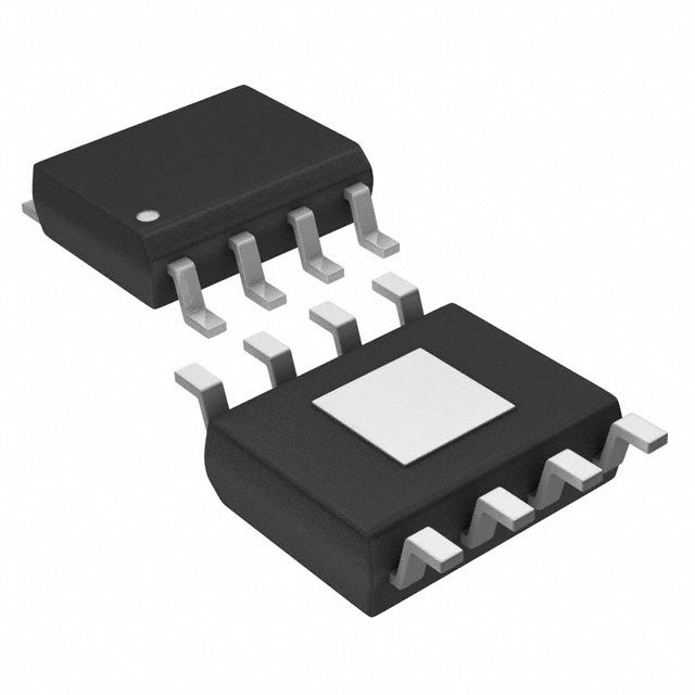
| 产品图片 |
|
| rohs | 符合RoHS无铅 / 符合限制有害物质指令(RoHS)规范要求 |
| 产品系列 | 放大器 IC,采样&保持放大器,Texas Instruments LF298M/NOPB- |
| 数据手册 | |
| 产品型号 | LF298M/NOPB |
| 产品 | Operational Amplifiers |
| 产品目录页面 | |
| 产品种类 | 采样&保持放大器 |
| 供应商器件封装 | 14-SOICN |
| 其它名称 | *LF298M/NOPB |
| 包装 | 管件 |
| 压摆率 | - |
| 商标 | Texas Instruments |
| 增益带宽积 | - |
| 安装类型 | 表面贴装 |
| 安装风格 | SMD/SMT |
| 封装 | Tube |
| 封装/外壳 | 14-SOIC(0.154",3.90mm 宽) |
| 封装/箱体 | SOIC-14 |
| 工作温度 | -25°C ~ 85°C |
| 工厂包装数量 | 55 |
| 带宽 | 1 MHz |
| 捕获时间 | 20 us |
| 放大器类型 | 采样和保持 |
| 最大工作温度 | + 85 C |
| 最小工作温度 | - 25 C |
| 标准包装 | 55 |
| 电压-电源,单/双 (±) | ±5 V ~ 18 V |
| 电压-输入失调 | 1mV |
| 电流-电源 | 4.5mA |
| 电流-输入偏置 | 5nA |
| 电流-输出/通道 | - |
| 电源电压-最大 | 18 V |
| 电源电压-最小 | 5 V |
| 电路数 | 1 |
| 系列 | LF298 |
| 输出类型 | - |
| 通道数量 | 2 Channel |


- 商务部:美国ITC正式对集成电路等产品启动337调查
- 曝三星4nm工艺存在良率问题 高通将骁龙8 Gen1或转产台积电
- 太阳诱电将投资9.5亿元在常州建新厂生产MLCC 预计2023年完工
- 英特尔发布欧洲新工厂建设计划 深化IDM 2.0 战略
- 台积电先进制程称霸业界 有大客户加持明年业绩稳了
- 达到5530亿美元!SIA预计今年全球半导体销售额将创下新高
- 英特尔拟将自动驾驶子公司Mobileye上市 估值或超500亿美元
- 三星加码芯片和SET,合并消费电子和移动部门,撤换高东真等 CEO
- 三星电子宣布重大人事变动 还合并消费电子和移动部门
- 海关总署:前11个月进口集成电路产品价值2.52万亿元 增长14.8%


PDF Datasheet 数据手册内容提取
Product Order Technical Tools & Support & Folder Now Documents Software Community LF198-N,LF298,LF398-N LF198A-N,LF398A-N SNOSBI3C–JULY2000–REVISEDOCTOBER2018 LFx98x Monolithic Sample-and-Hold Circuits 1 Features 3 Description • Operatesfrom±5-Vto ±18-VSupplies The LFx98x devices are monolithic sample-and-hold 1 circuits that use BI-FET technology to obtain ultrahigh • Lessthan10-μsAcquisitionTime DC accuracy with fast acquisition of signal and low • LogicInputCompatibleWithTTL,PMOS,CMOS droop rate. Operating as a unity-gain follower, DC • 0.5-mVTypicalHoldStepatCh=0.01 µF gain accuracy is 0.002% typical and acquisition time is as low as 6 µs to 0.01%. A bipolar input stage is • LowInputOffset used to achieve low offset voltage and wide • 0.002%GainAccuracy bandwidth. Input offset adjust is accomplished with a • LowOutputNoiseinHoldMode single pin and does not degrade input offset drift. The wide bandwidth allows the LFx98x to be included • InputCharacteristicsDoNotChangeDuringHold inside the feedback loop of 1-MHz operational Mode amplifiers without having stability problems. Input • HighSupplyRejectionRatioinSampleorHold impedance of 1010 Ω allows high-source impedances • WideBandwidth tobeusedwithoutdegradingaccuracy. • SpaceQualified,JM38510 P-channel junction FETs are combined with bipolar devices in the output amplifier to give droop rates as 2 Applications low as 5 mV/min with a 1-µF hold capacitor. The JFETs have much lower noise than MOS devices • RampGeneratorsWithVariableResetLevel used in previous designs and do not exhibit high • IntegratorsWithProgrammableResetLevel temperature instabilities. The overall design ensures • SynchronousCorrelators no feedthrough from input to output in the hold mode, • 2-ChannelSwitches evenforinputsignalsequaltothesupplyvoltages. • DCandACZeroing Logic inputs on the LFx98x are fully differential with low input current, allowing for direct connection to • StaircaseGenerators TTL, PMOS, and CMOS. Differential threshold is 1.4 V. The LFx98x will operate from ±5-V to ±18-V supplies. An A version is available with tightened electrical specifications. DeviceInformation(1) PARTNUMBER PACKAGE BODYSIZE(NOM) LF298,LF398-N SOIC(14) 8.65mm×3.91mm LFx98x TO-99(8) 9.08mm×9.08mm LF398-N PDIP(8) 9.81mm×6.35mm (1) For all available packages, see the orderable addendum at theendofthedatasheet. TypicalConnection AcquisitionTime 1 An IMPORTANT NOTICE at the end of this data sheet addresses availability, warranty, changes, use in safety-critical applications, intellectualpropertymattersandotherimportantdisclaimers.PRODUCTIONDATA.
LF198-N,LF298,LF398-N LF198A-N,LF398A-N SNOSBI3C–JULY2000–REVISEDOCTOBER2018 www.ti.com Table of Contents 1 Features.................................................................. 1 8.1 Overview.................................................................14 2 Applications........................................................... 1 8.2 FunctionalBlockDiagram.......................................14 3 Description............................................................. 1 8.3 FeatureDescription.................................................14 8.4 DeviceFunctionalModes........................................14 4 RevisionHistory..................................................... 2 9 ApplicationandImplementation........................ 15 5 PinConfigurationandFunctions......................... 3 9.1 ApplicationInformation............................................15 6 Specifications......................................................... 4 9.2 TypicalApplications................................................17 6.1 AbsoluteMaximumRatings......................................4 10 PowerSupplyRecommendations..................... 26 6.2 RecommendedOperatingConditions.......................4 11 Layout................................................................... 27 6.3 ThermalInformation..................................................4 6.4 ElectricalCharacteristics,LF198-NandLF298........5 11.1 LayoutGuidelines.................................................27 6.5 ElectricalCharacteristics,LF198A-N........................6 11.2 LayoutExample....................................................27 6.6 ElectricalCharacteristics,LF398-N...........................7 12 DeviceandDocumentationSupport................. 28 6.7 ElectricalCharacteristics,LF398A-N(OBSOLETE).8 12.1 DeviceSupport......................................................28 6.8 TypicalCharacteristics..............................................9 12.2 RelatedLinks........................................................28 7 ParameterMeasurementInformation................12 12.3 CommunityResources..........................................28 7.1 TTLandCMOS3V≤V (HiState)≤7V.......12 12.4 Trademarks...........................................................28 LOGIC 7.2 CMOS7V≤V (HiState)≤15V....................12 12.5 ElectrostaticDischargeCaution............................28 LOGIC 7.3 OperationalAmplifierDrive.....................................13 12.6 Glossary................................................................29 8 DetailedDescription............................................ 14 13 Mechanical,Packaging,andOrderable Information........................................................... 29 4 Revision History NOTE:Pagenumbersforpreviousrevisionsmaydifferfrompagenumbersinthecurrentversion. ChangesfromRevisionB(October2015)toRevisionC Page • UpdatedDeviceInformationandPinFunctionstables.......................................................................................................... 1 • SeparatedElectricalCharacteristicsintofourtables:LF198-NandLF298;LF198A-N;LF398-N;andLF398A-N (OBSOLETE).......................................................................................................................................................................... 5 ChangesfromRevisionA(July2000)toRevisionB Page • AddedESDRatingstable,ThermalInformationtable,FeatureDescriptionsection,DeviceFunctionalModes, ApplicationandImplementationsection,PowerSupplyRecommendationssection,Layoutsection,Deviceand DocumentationSupportsection,andMechanical,Packaging,andOrderableInformationsection....................................... 1 2 SubmitDocumentationFeedback Copyright©2000–2018,TexasInstrumentsIncorporated ProductFolderLinks:LF198-N LF298 LF398-NLF198A-N LF398A-N
LF198-N,LF298,LF398-N LF198A-N,LF398A-N www.ti.com SNOSBI3C–JULY2000–REVISEDOCTOBER2018 5 Pin Configuration and Functions PPackage 8-PinPDIP DPackage TopView 14-PinSOIC TopView LMCPackage 8-PinTO-99 TopView AmilitaryRETSelectricaltestspecificationisavailableonrequest.TheLF198-NmayalsobeprocuredtoStandard MilitaryDrawing#5962-8760801GAortoMIL-STD-38510partIDJM38510/12501SGA. PinFunctions PIN LF298,LF398-N LFx98x LF398-N TYPE(1) DESCRIPTION NAME SOIC-14 TO-99 PDIP-8 V+ 12 1 1 P Positivesupply OFFSETADJUST 14 2 2 A DCoffsetcompensationpin INPUT 1 3 3 A AnalogInput V– 3 4 4 P Negativesupply OUTPUT 7 5 5 O Output C 8 6 6 A Holdcapacitor h LOGICREFERENCE 10 7 7 I ReferenceforLOGICinput LOGIC 11 8 8 I LogicinputforSampleandHoldmodes NC 2,4,5,6,9,13 — — NA Noconnect (1) P=Power,G=Ground,I=Input,O=Output,A=Analog Copyright©2000–2018,TexasInstrumentsIncorporated SubmitDocumentationFeedback 3 ProductFolderLinks:LF198-N LF298 LF398-NLF198A-N LF398A-N
LF198-N,LF298,LF398-N LF198A-N,LF398A-N SNOSBI3C–JULY2000–REVISEDOCTOBER2018 www.ti.com 6 Specifications 6.1 Absolute Maximum Ratings overoperatingfree-airtemperaturerange(unlessotherwisenoted)(1)(2) MIN MAX UNIT Supplyvoltage ±18 V Powerdissipation (Packagelimitation,see (3)) 500 mW LF198-N,LF198A-N –55 125 °C Operatingambienttemperature LF298 –25 85 °C LF398-N,LF398A-N 0 70 °C Inputvoltage ±18 V Logic-to-logicreferencedifferentialvoltage(see (4)) 7 −30 V Outputshortcircuitduration Indefinite Holdcapacitorshortcircuitduration 10 sec Hpackage(soldering,10sec.) 260 °C Npackage(soldering,10sec.) 260 °C Leadtemperature Mpackage:vaporphase(60sec.) 215 °C Infrared(15sec.) 220 °C Storagetemperature,T –65 150 °C stg (1) StressesbeyondthoselistedunderAbsoluteMaximumRatingsmaycausepermanentdamagetothedevice.Thesearestressratings only,whichdonotimplyfunctionaloperationofthedeviceattheseoranyotherconditionsbeyondthoseindicatedunderRecommended OperatingConditions.Exposuretoabsolute-maximum-ratedconditionsforextendedperiodsmayaffectdevicereliability. (2) IfMilitary/Aerospacespecifieddevicesarerequired,pleasecontacttheTISalesOffice/Distributorsforavailabilityandspecifications. (3) ThemaximumpowerdissipationmustbederatedatelevatedtemperaturesandisdictatedbyT ,R ,andtheambienttemperature, JMAX θJA T .ThemaximumallowablepowerdissipationatanytemperatureisP =(T −T )/R ,orthenumbergivenintheAbsolute A D JMAX A θJA MaximumRatings,whicheverislower.Themaximumjunctiontemperature,T ,fortheLF198-NandLF198A-Nis150°C;forthe JMAX LF298,115°C;andfortheLF398-NandLF398A-N,100°C. (4) Althoughthedifferentialvoltagemaynotexceedthelimitsgiven,thecommon-modevoltageonthelogicpinsmaybeequaltothe supplyvoltageswithoutcausingdamagetothecircuit.Forproperlogicoperation,however,oneofthelogicpinsmustalwaysbeatleast 2Vbelowthepositivesupplyand3Vabovethenegativesupply. 6.2 Recommended Operating Conditions overoperatingfree-airtemperaturerange(unlessotherwisenoted) MIN NOM MAX UNIT Supplyvoltage ±15 V LF198-N,LF198A-N –55 125 T Ambienttemperature LF298 –25 85 °C J LF398-N,LF398A-N 0 70 6.3 Thermal Information LF398-N LF298,LF398-N LFx98x THERMALMETRIC(1) P(PDIP) D(SOIC) LMC(TO-99) UNIT 8PINS 14PINS 8PINS R Junction-to-ambientthermalresistance 48.9 80.6 85(2) °C/W θJA R Junction-to-case(top)thermalresistance 37.3 38.1 20 °C/W θJC(top) R Junction-to-boardthermalresistance 26.2 35.4 — °C/W θJB ψ Junction-to-topcharacterizationparameter 14.3 5.8 — °C/W JT ψ Junction-to-boardcharacterizationparameter 26.0 35.1 — °C/W JB (1) Formoreinformationabouttraditionalandnewthermalmetrics,seetheSemiconductorandICPackageThermalMetricsapplication report,SPRA953. (2) Boardmountin400LF/minairflow. 4 SubmitDocumentationFeedback Copyright©2000–2018,TexasInstrumentsIncorporated ProductFolderLinks:LF198-N LF298 LF398-NLF198A-N LF398A-N
LF198-N,LF298,LF398-N LF198A-N,LF398A-N www.ti.com SNOSBI3C–JULY2000–REVISEDOCTOBER2018 6.4 Electrical Characteristics, LF198-N and LF298 Thefollowingspecificationsapplyfor–V +3.5V≤V ≤+V –3.5V,+V =+15V,–V =–15V,T =T =25°C,C =0.01 S IN S S S A J h µF,R =10kΩ,LOGICREFERENCE=0V,LOGICHIGH=2.5V,LOGICLOW=0Vunlessotherwisespecified. L PARAMETER TESTCONDITIONS MIN TYP MAX UNIT T =25°C 1 3 mV Inputoffsetvoltage(1) J Fulltemperaturerange 5 mV T =25°C 5 25 nA Inputbiascurrent(1) J Fulltemperaturerange 75 nA Inputimpedance T =25°C 10 GΩ J T =25°C,R =10k 0.002% 0.005% J L Gainerror Fulltemperaturerange 0.02% Feedthroughattenuationratioat1kHz T =25°C,C =0.01µF 86 96 dB J h T =25°C,“HOLD”mode 0.5 2 Ω J Outputimpedance Fulltemperaturerange 4 Ω HOLDstep(2) T =25°C,C =0.01µF,V =0 0.5 2 mV J h OUT Supplycurrent(1) T ≥25°C 4.5 5.5 mA J Logicandlogicreferenceinputcurrent T =25°C 2 10 µA J Leakagecurrentintoholdcapacitor(1) T =25°C,holdmode(3) 30 100 pA J ΔV =10V,C =1000pF 4 µs OUT h Acquisitiontimeto0.1% C =0.01µF 20 µs H Holdcapacitorchargingcurrent V –V =2V 5 mA IN OUT Supplyvoltagerejectionratio V =0 80 110 dB OUT Differentiallogicthreshold T =25°C 0.8 1.4 2.4 V J (1) Theseparametersensuredoverasupplyvoltagerangeof±5to±18V,andaninputrangeof–V +3.5V≤V ≤+V –3.5V. S IN S (2) Holdstepissensitivetostraycapacitivecouplingbetweeninputlogicsignalsandtheholdcapacitor.1pF,forinstance,willcreatean additional0.5-mVstepwitha5-Vlogicswinganda0.01-µFholdcapacitor.Magnitudeoftheholdstepisinverselyproportionaltohold capacitorvalue. (3) Leakagecurrentismeasuredatajunctiontemperatureof25°C.Theeffectsofjunctiontemperatureriseduetopowerdissipationor elevatedambientcanbecalculatedbydoublingthe25°Cvalueforeach11°Cincreaseinchiptemperature.Leakageisguaranteedover fullinputsignalrange. Copyright©2000–2018,TexasInstrumentsIncorporated SubmitDocumentationFeedback 5 ProductFolderLinks:LF198-N LF298 LF398-NLF198A-N LF398A-N
LF198-N,LF298,LF398-N LF198A-N,LF398A-N SNOSBI3C–JULY2000–REVISEDOCTOBER2018 www.ti.com 6.5 Electrical Characteristics, LF198A-N Thefollowingspecificationsapplyfor–V +3.5V≤V ≤+V –3.5V,+V =+15V,–V =–15V,T =T =25°C,C =0.01 S IN S S S A J h µF,R =10kΩ,LOGICREFERENCE=0V,LOGICHIGH=2.5V,LOGICLOW=0Vunlessotherwisespecified. L PARAMETER TESTCONDITIONS MIN TYP MAX UNIT T =25°C 1 1 mV Inputoffsetvoltage(1) J Fulltemperaturerange 2 mV T =25°C 5 25 nA Inputbiascurrent(1) J Fulltemperaturerange 75 nA Inputimpedance T =25°C 10 GΩ J T =25°C,R =10k 0.002% 0.005% J L Gainerror Fulltemperaturerange 0.01% Feedthroughattenuationratioat1kHz T =25°C,C =0.01µF 86 96 dB J h T =25°C,“HOLD”mode 0.5 1 Ω J Outputimpedance Fulltemperaturerange 4 Ω HOLDstep(2) T =25°C,C =0.01µF,V =0 0.5 1 mV J h OUT Supplycurrent(1) T ≥25°C 4.5 5.5 mA J Logicandlogicreferenceinputcurrent T =25°C 2 10 µA J Leakagecurrentintoholdcapacitor(1) T =25°C,holdmode(3) 30 100 pA J ΔV =10V,C =1000pF 4 6 µs OUT h Acquisitiontimeto0.1% C =0.01µF 20 25 µs H Holdcapacitorchargingcurrent V –V =2V 5 mA IN OUT Supplyvoltagerejectionratio V =0 90 110 dB OUT Differentiallogicthreshold T =25°C 0.8 1.4 2.4 V J (1) Theseparametersensuredoverasupplyvoltagerangeof±5to±18V,andaninputrangeof–V +3.5V≤V ≤+V –3.5V. S IN S (2) Holdstepissensitivetostraycapacitivecouplingbetweeninputlogicsignalsandtheholdcapacitor.1pF,forinstance,willcreatean additional0.5-mVstepwitha5-Vlogicswinganda0.01-µFholdcapacitor.Magnitudeoftheholdstepisinverselyproportionaltohold capacitorvalue. (3) Leakagecurrentismeasuredatajunctiontemperatureof25°C.Theeffectsofjunctiontemperatureriseduetopowerdissipationor elevatedambientcanbecalculatedbydoublingthe25°Cvalueforeach11°Cincreaseinchiptemperature.Leakageisguaranteedover fullinputsignalrange. 6 SubmitDocumentationFeedback Copyright©2000–2018,TexasInstrumentsIncorporated ProductFolderLinks:LF198-N LF298 LF398-NLF198A-N LF398A-N
LF198-N,LF298,LF398-N LF198A-N,LF398A-N www.ti.com SNOSBI3C–JULY2000–REVISEDOCTOBER2018 6.6 Electrical Characteristics, LF398-N Thefollowingspecificationsapplyfor–V +3.5V≤V ≤+V –3.5V,+V =+15V,–V =–15V,T =T =25°C,C =0.01 S IN S S S A J h µF,R =10kΩ,LOGICREFERENCE=0V,LOGICHIGH=2.5V,LOGICLOW=0Vunlessotherwisespecified. L PARAMETER TESTCONDITIONS MIN TYP MAX UNIT T =25°C 2 7 mV Inputoffsetvoltage(1) J Fulltemperaturerange 10 mV T =25°C 10 50 nA Inputbiascurrent(1) J Fulltemperaturerange 100 nA Inputimpedance T =25°C 10 GΩ J T =25°C,R =10k 0.004% 0.01% J L Gainerror Fulltemperaturerange 0.02% Feedthroughattenuationratioat1kHz T =25°C,C =0.01µF 80 90 dB J h T =25°C,“HOLD”mode 0.5 4 Ω J Outputimpedance Fulltemperaturerange 6 Ω HOLDstep(2) T =25°C,C =0.01µF,V =0 1 2.5 mV J h OUT Supplycurrent(1) T ≥25°C 4.5 6.5 mA J Logicandlogicreferenceinputcurrent T =25°C 2 10 µA J Leakagecurrentintoholdcapacitor(1) T =25°C,holdmode(3) 30 200 pA J ΔV =10V,C =1000pF 4 µs OUT h Acquisitiontimeto0.1% C =0.01µF 20 µs H Holdcapacitorchargingcurrent V –V =2V 5 mA IN OUT Supplyvoltagerejectionratio V =0 80 110 dB OUT Differentiallogicthreshold T =25°C 0.8 1.4 2.4 V J (1) Theseparametersensuredoverasupplyvoltagerangeof±5to±18V,andaninputrangeof–V +3.5V≤V ≤+V –3.5V. S IN S (2) Holdstepissensitivetostraycapacitivecouplingbetweeninputlogicsignalsandtheholdcapacitor.1pF,forinstance,willcreatean additional0.5-mVstepwitha5-Vlogicswinganda0.01-µFholdcapacitor.Magnitudeoftheholdstepisinverselyproportionaltohold capacitorvalue. (3) Leakagecurrentismeasuredatajunctiontemperatureof25°C.Theeffectsofjunctiontemperatureriseduetopowerdissipationor elevatedambientcanbecalculatedbydoublingthe25°Cvalueforeach11°Cincreaseinchiptemperature.Leakageisguaranteedover fullinputsignalrange. Copyright©2000–2018,TexasInstrumentsIncorporated SubmitDocumentationFeedback 7 ProductFolderLinks:LF198-N LF298 LF398-NLF198A-N LF398A-N
LF198-N,LF298,LF398-N LF198A-N,LF398A-N SNOSBI3C–JULY2000–REVISEDOCTOBER2018 www.ti.com 6.7 Electrical Characteristics, LF398A-N (OBSOLETE) Thefollowingspecificationsapplyfor–V +3.5V≤V ≤+V –3.5V,+V =+15V,–V =–15V,T =T =25°C,C =0.01 S IN S S S A J h µF,R =10kΩ,LOGICREFERENCE=0V,LOGICHIGH=2.5V,LOGICLOW=0Vunlessotherwisespecified. L PARAMETER TESTCONDITIONS MIN TYP MAX UNIT T =25°C 2 2 mV Inputoffsetvoltage(1) J Fulltemperaturerange 3 mV T =25°C 10 25 nA Inputbiascurrent(1) J Fulltemperaturerange 50 nA Inputimpedance T =25°C 10 GΩ J T =25°C,R =10k 0.004% 0.005% J L Gainerror Fulltemperaturerange 0.01% Feedthroughattenuationratioat1kHz T =25°C,C =0.01µF 86 90 dB J h T =25°C,“HOLD”mode 0.5 1 Ω J Outputimpedance Fulltemperaturerange 6 Ω HOLDstep(2) T =25°C,C =0.01µF,V =0 1 1 mV J h OUT Supplycurrent(1) T ≥25°C 4.5 6.5 mA J Logicandlogicreferenceinputcurrent T =25°C 2 10 µA J Leakagecurrentintoholdcapacitor(1) T =25°C,holdmode(3) 30 100 pA J ΔV =10V,C =1000pF 4 6 µs OUT h Acquisitiontimeto0.1% C =0.01µF 20 25 µs H Holdcapacitorchargingcurrent V –V =2V 5 mA IN OUT Supplyvoltagerejectionratio V =0 90 110 dB OUT Differentiallogicthreshold T =25°C 0.8 1.4 2.4 V J (1) Theseparametersensuredoverasupplyvoltagerangeof±5to±18V,andaninputrangeof–V +3.5V≤V ≤+V –3.5V. S IN S (2) Holdstepissensitivetostraycapacitivecouplingbetweeninputlogicsignalsandtheholdcapacitor.1pF,forinstance,willcreatean additional0.5-mVstepwitha5-Vlogicswinganda0.01-µFholdcapacitor.Magnitudeoftheholdstepisinverselyproportionaltohold capacitorvalue. (3) Leakagecurrentismeasuredatajunctiontemperatureof25°C.Theeffectsofjunctiontemperatureriseduetopowerdissipationor elevatedambientcanbecalculatedbydoublingthe25°Cvalueforeach11°Cincreaseinchiptemperature.Leakageisguaranteedover fullinputsignalrange. 8 SubmitDocumentationFeedback Copyright©2000–2018,TexasInstrumentsIncorporated ProductFolderLinks:LF198-N LF298 LF398-NLF198A-N LF398A-N
LF198-N,LF298,LF398-N LF198A-N,LF398A-N www.ti.com SNOSBI3C–JULY2000–REVISEDOCTOBER2018 6.8 Typical Characteristics Figure1.ApertureTime Figure2.DielectricAbsorptionErrorinHoldCapacitor Figure3.DynamicSamplingError Figure4.OutputDroopRate Figure5.HoldStep Figure6.HoldSettlingTime Copyright©2000–2018,TexasInstrumentsIncorporated SubmitDocumentationFeedback 9 ProductFolderLinks:LF198-N LF298 LF398-NLF198A-N LF398A-N
LF198-N,LF298,LF398-N LF198A-N,LF398A-N SNOSBI3C–JULY2000–REVISEDOCTOBER2018 www.ti.com Typical Characteristics (continued) Figure7.LeakageCurrentintoHoldCapacitor Figure8.PhaseandGain(InputtoOutput,SmallSignal) Figure9.GainError Figure10.PowerSupplyRejection Figure11.OutputShortCircuitCurrent Figure12.OutputNoise 10 SubmitDocumentationFeedback Copyright©2000–2018,TexasInstrumentsIncorporated ProductFolderLinks:LF198-N LF298 LF398-NLF198A-N LF398A-N
LF198-N,LF298,LF398-N LF198A-N,LF398A-N www.ti.com SNOSBI3C–JULY2000–REVISEDOCTOBER2018 Typical Characteristics (continued) Figure13.InputBiasCurrent Figure14.FeedthroughRejectionRatio(HoldMode) Figure15.HoldStepvsInputVoltage Figure16.OutputTransientatStartofSampleMode Figure17.OutputTransientatStartofHoldMode Copyright©2000–2018,TexasInstrumentsIncorporated SubmitDocumentationFeedback 11 ProductFolderLinks:LF198-N LF298 LF398-NLF198A-N LF398A-N
LF198-N,LF298,LF398-N LF198A-N,LF398A-N SNOSBI3C–JULY2000–REVISEDOCTOBER2018 www.ti.com 7 Parameter Measurement Information 7.1 TTL and CMOS 3 V ≤ V (Hi State) ≤ 7 V LOGIC Threshold=1.4V Figure18. SampleWhenLogicHighWithTTLandCMOSBiasing Threshold=1.4V Selectfor2.8Vatpin8 Figure19. SampleWhenLogicLowWithTTLandCMOSBiasing 7.2 CMOS 7 V ≤ V (Hi State) ≤ 15 V LOGIC Threshold=0.6(V+)+1.4V Figure20. SampleWhenLogicHighWithCMOSBiasing 12 SubmitDocumentationFeedback Copyright©2000–2018,TexasInstrumentsIncorporated ProductFolderLinks:LF198-N LF298 LF398-NLF198A-N LF398A-N
LF198-N,LF298,LF398-N LF198A-N,LF398A-N www.ti.com SNOSBI3C–JULY2000–REVISEDOCTOBER2018 CMOS 7 V ≤ V (Hi State) ≤ 15 V (continued) LOGIC Threshold=0.6(V+)–1.4V Figure21. SampleWhenLogicLowWithCMOSBiasing 7.3 Operational Amplifier Drive Threshold≈+4V Figure22. SampleWhenLogicHighWithOperationalAmplifierBiasing Threshold=−4V Figure23. SampleWhenLogicLowWithOperationalAmplifierBiasing Copyright©2000–2018,TexasInstrumentsIncorporated SubmitDocumentationFeedback 13 ProductFolderLinks:LF198-N LF298 LF398-NLF198A-N LF398A-N
LF198-N,LF298,LF398-N LF198A-N,LF398A-N SNOSBI3C–JULY2000–REVISEDOCTOBER2018 www.ti.com 8 Detailed Description 8.1 Overview The LFx98x devices are monolithic sample-and-hold circuits that utilize BI-FET technology to obtain ultrahigh DC accuracy with fast acquisition of signal and low droop rate. Operating as a unity-gain follower, DC gain accuracy is 0.002% typical and acquisition time is as low as 6 µs to 0.01%. A bipolar input stage is used to achieve low offset voltage and wide bandwidth. Input offset adjust is accomplished with a single pin, and does not degrade input offset drift. The wide bandwidth allows the LF198-N to be included inside the feedback loop of 1-MHz operational amplifier without having stability problems. Input impedance of 1010 Ω allows high-source impedancestobeusedwithoutdegradingaccuracy. 8.2 Functional Block Diagram 8.3 Feature Description TheLFx98xOUTPUTtrackstheINPUTsignalbycharginganddischargingtheholdcapacitor.TheOUTPUTcan be held at any given time by pulling the LOGIC input low relative to the LOGIC REFERENCE voltage and resume sampling when LOGIC returns high. Additionally, the OFFSET pin can be used to zero the offset voltage presentattheINPUT. 8.4 Device Functional Modes The LFx98x devices have a sample mode and hold mode controlled by the LOGIC voltage relative to the LOGIC REFERENCE voltage. The device is in sample mode when the LOGIC input is pulled high relative to the LOGIC REFERENCEvoltageandinholdmodewhentheLOGICinputispulledlowrelativetotheLOGICREFERENCE. In sample mode, the output is tracking the input signal by charging and discharging the hold capacitor. Smaller values of hold capacitance will allow the output to track faster signals. In hold mode the input signal is disconnected from the signal path and the output retains the value on the hold capacitor. Larger values of capacitancewillhaveasmallerdrooprateasshowninFigure4. 14 SubmitDocumentationFeedback Copyright©2000–2018,TexasInstrumentsIncorporated ProductFolderLinks:LF198-N LF298 LF398-NLF198A-N LF398A-N
LF198-N,LF298,LF398-N LF198A-N,LF398A-N www.ti.com SNOSBI3C–JULY2000–REVISEDOCTOBER2018 9 Application and Implementation NOTE Information in the following applications sections is not part of the TI component specification, and TI does not warrant its accuracy or completeness. TI’s customers are responsible for determining suitability of components for their purposes. Customers should validateandtesttheirdesignimplementationtoconfirmsystemfunctionality. 9.1 Application Information 9.1.1 HoldCapacitor Holdstep,acquisitiontime,anddroopratearethemajortrade-offsintheselectionofaholdcapacitorvalue.Size and cost may also become important for larger values. Use of the curves included with this data sheet should be helpful in selecting a reasonable value of capacitance. Keep in mind that for fast repetition rates or tracking fast signals,thecapacitordrivecurrentsmaycauseasignificanttemperatureriseintheLF198-N. Asignificantsourceoferrorinanaccuratesampleandholdcircuitisdielectricabsorptionintheholdcapacitor.A mylar cap, for instance, may sag back up to 0.2% after a quick change in voltage. A long sample time is required before the circuit can be put back into the hold mode with this type of capacitor. Dielectrics with very low hysteresis are polystyrene, polypropylene, and Teflon. Other types such as mica and polycarbonate are not nearly as good. The advantage of polypropylene over polystyrene is that it extends the maximum ambient temperature from 85°C to 100°C. Most ceramic capacitors are unusable with > 1% hysteresis. Ceramic NPO or COG capacitors are now available for 125°C operation and also have low dielectric absorption. For more exact data, see Figure 2. The hysteresis numbers on the curve are final values, taken after full relaxation. The hysteresis error can be significantly reduced if the output of the LF198-N is digitized quickly after the hold mode is initiated. The hysteresis relaxation time constant in polypropylene, for instance, is 10 to 50 ms. If A-to-D conversioncanbemadewithin1ms,hysteresiserrorwillbereducedbyafactoroften. 9.1.2 DCandACZeroing DC zeroing is accomplished by connecting the offset adjust pin to the wiper of a 1-kΩ potentiometer, which has one end tied to V+ and the other end tied through a resistor to ground. The resistor should be selected to give approximately0.6mAthroughthe1-kΩpotentiometer. ACzeroing(holdstepzeroing)canbeobtainedbyaddinganinverterwiththeadjustmentpottiedinputtooutput. A 10-pF capacitor from the wiper to the hold capacitor will give ±4-mV hold step adjustment with a 0.01-µF hold capacitorand5-Vlogicsupply.Forlargerlogicswings,asmallercapacitor(< 10pF)maybeused. 9.1.3 LogicRiseTime For proper operation, logic signals into the LF198-N must have a minimum dV/dt of 1.0 V/µs. Slower signals will cause excessive hold step. If a R/C network is used in front of the logic input for signal delay, calculate the slope ofthewaveformatthethresholdpointtoensurethatitisatleast1.0V/µs. 9.1.4 SamplingDynamicSignals Sample error to moving input signals probably causes more confusion among sample-and-hold users than any other parameter. The primary reason for this is that many users make the assumption that the sample and hold amplifier is truly locked on to the input signal while in the sample mode. In actuality, there are finite phase delays through the circuit creating an input-output differential for fast moving signals. In addition, although the output may have settled, the hold capacitor has an additional lag due to the 300-Ω series resistor on the chip. This meansthatatthemomentthe holdcommandarrives,thehold capacitor voltage may be somewhat different than the actual analog input. The effect of these delays is opposite to the effect created by delays in the logic which switches the circuit from sample to hold. For example, consider an analog input of 20 Vp–p at 10 kHz. Maximum dV/dt is 0.6 V/µs. With no analog phase delay and 100-ns logic delay, one could expect up to (0.1 µs) (0.6V/µs) = 60 mVerror if the hold signal arrived near maximum dV/dt of the input. A positive-going input would give a Copyright©2000–2018,TexasInstrumentsIncorporated SubmitDocumentationFeedback 15 ProductFolderLinks:LF198-N LF298 LF398-NLF198A-N LF398A-N
LF198-N,LF298,LF398-N LF198A-N,LF398A-N SNOSBI3C–JULY2000–REVISEDOCTOBER2018 www.ti.com Application Information (continued) 60-mV error. Now assume a 1-MHz (3-dB) bandwidth for the overall analog loop. This generates a phase delay of 160 ns. If the hold capacitor sees this exact delay, then error due to analog delay will be (0.16 µs) (0.6 V/µs) = –96 mV. Total output error is 60 mV (digital) –96 mV (analog) for a total of –36 mV. To add to the confusion, analog delay is proportioned to hold capacitor value while digital delay remains constant. A family of curves (dynamicsamplingerror)isincludedtohelpestimateerrors. Figure 1 has been included for sampling conditions where the input is steady during the sampling period, but may experience a sudden change nearly coincident with the hold command. This curve is based on a 1-mV error fedintotheoutput. Figure6 indicatesthetimerequiredfortheoutputtosettleto1mVaftertheholdcommand. 9.1.5 DigitalFeedthrough Fast rise time logic signals can cause hold errors by feeding externally into the analog input at the same time the amplifier is put into the hold mode. To minimize this problem, board layout should keep logic lines as far as possiblefromtheanaloginputandtheC pin.Groundedguardingtracesmayalsobeusedaroundtheinputline, h especially if it is driven from a high impedance source. Reducing high amplitude logic signals to 2.5 V will also help. Use10-pinlayout.GuardaroundC istiedtooutput. H Figure24. GuardingTechnique 16 SubmitDocumentationFeedback Copyright©2000–2018,TexasInstrumentsIncorporated ProductFolderLinks:LF198-N LF298 LF398-NLF198A-N LF398A-N
LF198-N,LF298,LF398-N LF198A-N,LF398A-N www.ti.com SNOSBI3C–JULY2000–REVISEDOCTOBER2018 9.2 Typical Applications 9.2.1 X1000SampleandHold The circuit configuration in Figure 25 shows how to incorporate an amplification factor of 1000 into the sample and hold stage. This may be particularly useful if the input signal has a very low amplitude. Equation 1 provides theappropriatevalueofcapacitancefortheCOMP2pincapacitanceoftheLM108. *Forlowergains,theLM108mustbefrequencycompensated Figure25. X1000SampleandHold 100 Use» pFfromcomp2toground A V (1) 9.2.1.1 DesignRequirements Assume an unbuffered analog to digital converter with 1-Vpp dynamic range is used in a system which needs to sample an input signal with only 1-mVpp amplitude. Using the LF198-N and LM108 connect the input signal so thatthemaximumdynamicrangeisusedbythe1-Vppdataconverter. 9.2.1.2 DetailedDesignProcedure ConnecttheLFx98xandLM108asshowninFigure25.Tomaximizethedynamicrangeof1Vppagainfactorof 1000xisneeded.SetR3to1MΩandR4to1kΩtogiveanoninvertinggainof1001.ThecalculatedvalueofC1 is0.1pFaccordingtoEquation1,whichisnegligiblysmallandmaybeleftoffofthedesign. Copyright©2000–2018,TexasInstrumentsIncorporated SubmitDocumentationFeedback 17 ProductFolderLinks:LF198-N LF298 LF398-NLF198A-N LF398A-N
LF198-N,LF298,LF398-N LF198A-N,LF398A-N SNOSBI3C–JULY2000–REVISEDOCTOBER2018 www.ti.com Typical Applications (continued) 9.2.1.3 ApplicationCurves The feedthrough rejection ratio of the LF198-N is extremely good and provides good isolation for a wide variety of hold capacitors as Figure 26 shows. Additionally, the output transient settles almost completely after 0.8 µs andwouldbereadytosampleasshowninFigure27. Figure26.FeedthroughRejectionRatio(HoldMode) Figure27.OutputTransientatStartofHoldMode 9.2.2 SampleandDifferenceCircuit The LFx98x may be used as a sample and difference circuit as shown in Figure 28 where the output follows the inputinholdmode. V =V +∆V (HOLDMODE) OUT B IN Figure28. SampleandDifferenceCircuit 18 SubmitDocumentationFeedback Copyright©2000–2018,TexasInstrumentsIncorporated ProductFolderLinks:LF198-N LF298 LF398-NLF198A-N LF398A-N
LF198-N,LF298,LF398-N LF198A-N,LF398A-N www.ti.com SNOSBI3C–JULY2000–REVISEDOCTOBER2018 Typical Applications (continued) 9.2.3 RampGeneratorWithVariableResetLevel The circuit configuration shown in Figure 29 generates a ramp signal with variable reset level. The rise or fall timemaybecomputedbyEquation2. Figure29. RampGeneratorWithVariableResetLevel DV 1.2V = DT (R2)(C ) h (2) 9.2.4 IntegratorWithProgrammableResetLevel The LFx98x may be used with LM308 to create an integrator circuit with programmable reset level as shown in Figure30.TheintegratedoutputvoltageinholdmodeiscomputedwithEquation3. Figure30. IntegratorWithProgrammableResetLevel VOUT (HoldMode)=éê 1 òtVIN dtùú+éëVRùû ë(R1)(Ch) 0 û (3) Copyright©2000–2018,TexasInstrumentsIncorporated SubmitDocumentationFeedback 19 ProductFolderLinks:LF198-N LF298 LF398-NLF198A-N LF398A-N
LF198-N,LF298,LF398-N LF198A-N,LF398A-N SNOSBI3C–JULY2000–REVISEDOCTOBER2018 www.ti.com Typical Applications (continued) 9.2.5 OutputHoldsatAverageofSampledInput The LFx98x can be used to identify the average value of the input signal and hold the corresponding voltage on the output. Connect R and C as shown in Figure 31. The corresponding values may be calculated with h h Equation4. Figure31. OutputHoldsatAverageofSampledInput 1 Select(R )(C )? h h 2pf (Min) IN (4) 9.2.6 IncreasedSlewCurrent The slew current can be increased by connecting opposing diodes from the OUTPUT to the HOLD CAPACITOR pinsasshowninFigure32. Figure32. IncreasedSlewCurrent 20 SubmitDocumentationFeedback Copyright©2000–2018,TexasInstrumentsIncorporated ProductFolderLinks:LF198-N LF298 LF398-NLF198A-N LF398A-N
LF198-N,LF298,LF398-N LF198A-N,LF398A-N www.ti.com SNOSBI3C–JULY2000–REVISEDOCTOBER2018 Typical Applications (continued) 9.2.7 ResetStabilizedAmplifier The LFx98x may be used with LH0042H to create a reset stabilized amplifier with a gain of 1000 as shown in Figure33. V ≤20 µV(Notrim) Z ≈1MΩ OS IN Figure33. ResetStabilizedAmplifier DV OS »30mV/sec Dt (5) DV OS »0.1mV/ºC DT (6) Copyright©2000–2018,TexasInstrumentsIncorporated SubmitDocumentationFeedback 21 ProductFolderLinks:LF198-N LF298 LF398-NLF198A-N LF398A-N
LF198-N,LF298,LF398-N LF198A-N,LF398A-N SNOSBI3C–JULY2000–REVISEDOCTOBER2018 www.ti.com Typical Applications (continued) 9.2.8 FastAcquisition,LowDroopSampleandHold Two LFx98x devices may be used along with LM3905 TIMER to create a fast acquisition, low droop sample and holdcircuitasshowninFigure34. Figure34. FastAcquisition,LowDroopSampleandHold 22 SubmitDocumentationFeedback Copyright©2000–2018,TexasInstrumentsIncorporated ProductFolderLinks:LF198-N LF298 LF398-NLF198A-N LF398A-N
LF198-N,LF298,LF398-N LF198A-N,LF398A-N www.ti.com SNOSBI3C–JULY2000–REVISEDOCTOBER2018 Typical Applications (continued) 9.2.9 SynchronousCorrelatorforRecoveringSignalsBelowNoiseLevel The LFx98x may be used with two LM122H TIMER devices to create a synchronous correlator for recovering signalsbelownoiselevelasshowninFigure35. Figure35. SynchronousCorrelatorforRecoveringSignalsBelowNoiseLevel 9.2.10 2-ChannelSwitch The HOLD CAPACITOR pin could be alternatively used as a second input to create a 2-channel switch shown Figure36 Figure36. 2-ChannelSwitch IntheconfigurationofFigure36,inputsignalAandinputsignalBhavethecharacteristicslistedinTable1. Copyright©2000–2018,TexasInstrumentsIncorporated SubmitDocumentationFeedback 23 ProductFolderLinks:LF198-N LF298 LF398-NLF198A-N LF398A-N
LF198-N,LF298,LF398-N LF198A-N,LF398A-N SNOSBI3C–JULY2000–REVISEDOCTOBER2018 www.ti.com Typical Applications (continued) Table1.2-ChannelSwitchCharacteristics A B Gain 1±0.02% 1±0.2% ZIN 1010Ω 47kΩ BW ≈1MHz ≈400kHz Crosstalk@1kHz –90dB –90dB Offset ≤6mV ≤75mV 9.2.11 DCandACZeroing The LFLFx98x features an OFFSET ADJUST pin which can be connected to a potentiometer to zero the DC offset. Additionally, an inverter may be connected with an AC-coupled potentiometer to the HOLD CAPACITOR pintocreateaDC-andAC-zeroingcircuitasshowninFigure37. Figure37. DCandACZeroing 24 SubmitDocumentationFeedback Copyright©2000–2018,TexasInstrumentsIncorporated ProductFolderLinks:LF198-N LF298 LF398-NLF198A-N LF398A-N
LF198-N,LF298,LF398-N LF198A-N,LF398A-N www.ti.com SNOSBI3C–JULY2000–REVISEDOCTOBER2018 9.2.12 StaircaseGenerator TheLFx98xcanbeconnectedasshowninFigure38tocreateastaircasegenerator. *Selectforstepheight:50kΩ→1-VStep. Figure38. StaircaseGenerator 9.2.13 DifferentialHold TwoLFx98xdevicesmaybeconnectedasshowninFigure39tocreateadifferentialholdcircuit. Figure39. DifferentialHold Copyright©2000–2018,TexasInstrumentsIncorporated SubmitDocumentationFeedback 25 ProductFolderLinks:LF198-N LF298 LF398-NLF198A-N LF398A-N
LF198-N,LF298,LF398-N LF198A-N,LF398A-N SNOSBI3C–JULY2000–REVISEDOCTOBER2018 www.ti.com 9.2.14 CapacitorHysteresisCompensation TheLFx98xdevicesmaybeusedforcapacitorhysteresiscompensationasshowninFigure40. *SelectfortimeconstantC1= τ/100kΩ **Adjustforamplitude Figure40. CapacitorHysteresisCompensation 10 Power Supply Recommendations The LFx98x devices are rated for a typical supply voltage of ±15 V. To achieve noise immunity as appropriate to theapplication,itisimportanttousegoodprinted-circuit-boardlayoutpracticesforpowersupplyrailsandplanes, as well as using bypass capacitors connected between the power supply pins and ground. All bypass capacitors must be rated to handle the supply voltage and be decoupled to ground. TI recommends to decouple each supply with two capacitors; a small value ceramic capacitor (approximately 0.1 μF) placed close to the supply pin in addition to a large value Tantalum or Ceramic (≥ 10 μF). The large capacitor can be shared by more than one deviceifnecessary.Thesmallceramiccapacitormaintainslowsupplyimpedanceathigherfrequencieswhilethe largecapacitorwillactasthechargebucketforfastloadcurrentspikesattheopampoutput.Thecombinationof these capacitors will provide supply decoupling and will help maintain stable operation for most loading conditions. 26 SubmitDocumentationFeedback Copyright©2000–2018,TexasInstrumentsIncorporated ProductFolderLinks:LF198-N LF298 LF398-NLF198A-N LF398A-N
LF198-N,LF298,LF398-N LF198A-N,LF398A-N www.ti.com SNOSBI3C–JULY2000–REVISEDOCTOBER2018 11 Layout 11.1 Layout Guidelines Take care to minimize the loop area formed by the bypass capacitor connection between supply pins and ground. A ground plane underneath the device is recommended; any bypass components to ground should have a nearby via to the ground plane. The optimum bypass capacitor placement is closest to the corresponding supply pin. Use of thicker traces from the bypass capacitors to the corresponding supply pins will lower the power supply inductance and provide a more stable power supply. The feedback components should be placed asclosetothedeviceaspossibletominimizestrayparasitics. 11.2 Layout Example Figure41showsanexampleschematicandlayoutfortheLFx98x8-pinPDIPpackage. LFx98M U1 1 OFFSET 14 INPUT INPUT OFF ADJ ADJUST 2 13 NNCC NC V+ C3 C4 3 12 V– VV–- V+ 0.1 µF 10 µF C1 C2 4 11 10 µF 0.1 µF NC LOGIC LOGIC 5 LOGIC 10 NC LOG REF REFERENCE 6 9 NC NC 7 8 OUTPUT OUTPUT CH Ch CH Figure41. SchematicExample Figure42. LayoutExample Copyright©2000–2018,TexasInstrumentsIncorporated SubmitDocumentationFeedback 27 ProductFolderLinks:LF198-N LF298 LF398-NLF198A-N LF398A-N
LF198-N,LF298,LF398-N LF198A-N,LF398A-N SNOSBI3C–JULY2000–REVISEDOCTOBER2018 www.ti.com 12 Device and Documentation Support 12.1 Device Support 12.1.1 DeviceNomenclature • Hold Step: The voltage step at the output of the sample and hold when switching from sample mode to hold modewithasteady(DC)analoginputvoltage.Logicswingis5V. • Acquisition Time: The time required to acquire a new analog input voltage with an output step of 10 V. Acquisition time is not just the time required for the output to settle, but also includes the time required for all internalnodestosettlesothattheoutputassumesthepropervaluewhenswitchedtotheholdmode. • Gain Error: The ratio of output voltage swing to input voltage swing in the sample mode expressed as a per centdifference. • Hold Settling Time: The time required for the output to settle within 1 mV of final value after the hold logic command. • Dynamic Sampling Error: The error introduced into the held output due to a changing analog input at the time the hold command is given. Error is expressed in mV with a given hold capacitor value and input slew rate.Thiserrortermoccursevenforlongsampletimes. • Aperture Time: The delay required between hold command and an input analog transition, so that the transitiondoesnotaffecttheheldoutput. 12.2 Related Links The table below lists quick access links. Categories include technical documents, support and community resources,toolsandsoftware,andquickaccesstosampleorbuy. Table2.RelatedLinks TECHNICAL TOOLS& SUPPORT& PARTS PRODUCTFOLDER SAMPLE&BUY DOCUMENTS SOFTWARE COMMUNITY LF198-N Clickhere Clickhere Clickhere Clickhere Clickhere LF298 Clickhere Clickhere Clickhere Clickhere Clickhere LF398-N Clickhere Clickhere Clickhere Clickhere Clickhere LF198A-N Clickhere Clickhere Clickhere Clickhere Clickhere LF398A-N(Obsolete) Clickhere Clickhere Clickhere Clickhere Clickhere 12.3 Community Resources The following links connect to TI community resources. Linked contents are provided "AS IS" by the respective contributors. They do not constitute TI specifications and do not necessarily reflect TI's views; see TI's Terms of Use. TIE2E™OnlineCommunity TI'sEngineer-to-Engineer(E2E)Community.Createdtofostercollaboration amongengineers.Ate2e.ti.com,youcanaskquestions,shareknowledge,exploreideasandhelp solveproblemswithfellowengineers. DesignSupport TI'sDesignSupport QuicklyfindhelpfulE2Eforumsalongwithdesignsupporttoolsand contactinformationfortechnicalsupport. 12.4 Trademarks E2EisatrademarkofTexasInstruments. Allothertrademarksarethepropertyoftheirrespectiveowners. 12.5 Electrostatic Discharge Caution Thesedeviceshavelimitedbuilt-inESDprotection.Theleadsshouldbeshortedtogetherorthedeviceplacedinconductivefoam duringstorageorhandlingtopreventelectrostaticdamagetotheMOSgates. 28 SubmitDocumentationFeedback Copyright©2000–2018,TexasInstrumentsIncorporated ProductFolderLinks:LF198-N LF298 LF398-NLF198A-N LF398A-N
LF198-N,LF298,LF398-N LF198A-N,LF398A-N www.ti.com SNOSBI3C–JULY2000–REVISEDOCTOBER2018 12.6 Glossary SLYZ022—TIGlossary. Thisglossarylistsandexplainsterms,acronyms,anddefinitions. 13 Mechanical, Packaging, and Orderable Information The following pages include mechanical, packaging, and orderable information. This information is the most current data available for the designated devices. This data is subject to change without notice and revision of thisdocument.Forbrowser-basedversionsofthisdatasheet,refertotheleft-handnavigation. Copyright©2000–2018,TexasInstrumentsIncorporated SubmitDocumentationFeedback 29 ProductFolderLinks:LF198-N LF298 LF398-NLF198A-N LF398A-N
PACKAGE OPTION ADDENDUM www.ti.com 6-Feb-2020 PACKAGING INFORMATION Orderable Device Status Package Type Package Pins Package Eco Plan Lead/Ball Finish MSL Peak Temp Op Temp (°C) Device Marking Samples (1) Drawing Qty (2) (6) (3) (4/5) LF198AH/NOPB ACTIVE TO-99 LMC 8 500 Green (RoHS Call TI Level-1-NA-UNLIM -55 to 125 ( LF198AH, LF198AH & no Sb/Br) ) LF198H ACTIVE TO-99 LMC 8 500 TBD Call TI Call TI -55 to 125 ( LF198H, LF198H) LF198H/NOPB ACTIVE TO-99 LMC 8 500 Green (RoHS Call TI Level-1-NA-UNLIM -55 to 125 ( LF198H, LF198H) & no Sb/Br) LF298M NRND SOIC D 14 55 TBD Call TI Call TI -25 to 85 LF298M LF298M/NOPB ACTIVE SOIC D 14 55 Green (RoHS SN Level-1-260C-UNLIM -25 to 85 LF298M & no Sb/Br) LF298MX NRND SOIC D 14 2500 TBD Call TI Call TI -25 to 85 LF298M LF298MX/NOPB ACTIVE SOIC D 14 2500 Green (RoHS SN Level-1-260C-UNLIM -25 to 85 LF298M & no Sb/Br) LF398AN/NOPB ACTIVE PDIP P 8 40 Green (RoHS SN Level-1-NA-UNLIM 0 to 70 LF & no Sb/Br) 398AN LF398H ACTIVE TO-99 LMC 8 500 Green (RoHS Call TI Level-1-NA-UNLIM 0 to 70 LF398H & no Sb/Br) LF398H/NOPB ACTIVE TO-99 LMC 8 500 Green (RoHS Call TI Level-1-NA-UNLIM 0 to 70 ( LF398H, LF398H) & no Sb/Br) LF398M NRND SOIC D 14 55 TBD Call TI Call TI 0 to 70 LF398M LF398M/NOPB ACTIVE SOIC D 14 55 Green (RoHS SN Level-1-260C-UNLIM 0 to 70 LF398M & no Sb/Br) LF398MX/NOPB ACTIVE SOIC D 14 2500 Green (RoHS SN Level-1-260C-UNLIM 0 to 70 LF398M & no Sb/Br) LF398N/NOPB ACTIVE PDIP P 8 40 Green (RoHS SN Level-1-NA-UNLIM 0 to 70 LF & no Sb/Br) 398N (1) The marketing status values are defined as follows: ACTIVE: Product device recommended for new designs. LIFEBUY: TI has announced that the device will be discontinued, and a lifetime-buy period is in effect. NRND: Not recommended for new designs. Device is in production to support existing customers, but TI does not recommend using this part in a new design. PREVIEW: Device has been announced but is not in production. Samples may or may not be available. OBSOLETE: TI has discontinued the production of the device. Addendum-Page 1
PACKAGE OPTION ADDENDUM www.ti.com 6-Feb-2020 (2) RoHS: TI defines "RoHS" to mean semiconductor products that are compliant with the current EU RoHS requirements for all 10 RoHS substances, including the requirement that RoHS substance do not exceed 0.1% by weight in homogeneous materials. Where designed to be soldered at high temperatures, "RoHS" products are suitable for use in specified lead-free processes. TI may reference these types of products as "Pb-Free". RoHS Exempt: TI defines "RoHS Exempt" to mean products that contain lead but are compliant with EU RoHS pursuant to a specific EU RoHS exemption. Green: TI defines "Green" to mean the content of Chlorine (Cl) and Bromine (Br) based flame retardants meet JS709B low halogen requirements of <=1000ppm threshold. Antimony trioxide based flame retardants must also meet the <=1000ppm threshold requirement. (3) MSL, Peak Temp. - The Moisture Sensitivity Level rating according to the JEDEC industry standard classifications, and peak solder temperature. (4) There may be additional marking, which relates to the logo, the lot trace code information, or the environmental category on the device. (5) Multiple Device Markings will be inside parentheses. Only one Device Marking contained in parentheses and separated by a "~" will appear on a device. If a line is indented then it is a continuation of the previous line and the two combined represent the entire Device Marking for that device. (6) Lead/Ball Finish - Orderable Devices may have multiple material finish options. Finish options are separated by a vertical ruled line. Lead/Ball Finish values may wrap to two lines if the finish value exceeds the maximum column width. Important Information and Disclaimer:The information provided on this page represents TI's knowledge and belief as of the date that it is provided. TI bases its knowledge and belief on information provided by third parties, and makes no representation or warranty as to the accuracy of such information. Efforts are underway to better integrate information from third parties. TI has taken and continues to take reasonable steps to provide representative and accurate information but may not have conducted destructive testing or chemical analysis on incoming materials and chemicals. TI and TI suppliers consider certain information to be proprietary, and thus CAS numbers and other limited information may not be available for release. In no event shall TI's liability arising out of such information exceed the total purchase price of the TI part(s) at issue in this document sold by TI to Customer on an annual basis. Addendum-Page 2
PACKAGE MATERIALS INFORMATION www.ti.com 29-Sep-2019 TAPE AND REEL INFORMATION *Alldimensionsarenominal Device Package Package Pins SPQ Reel Reel A0 B0 K0 P1 W Pin1 Type Drawing Diameter Width (mm) (mm) (mm) (mm) (mm) Quadrant (mm) W1(mm) LF298MX SOIC D 14 2500 330.0 16.4 6.5 9.35 2.3 8.0 16.0 Q1 LF298MX/NOPB SOIC D 14 2500 330.0 16.4 6.5 9.35 2.3 8.0 16.0 Q1 LF398MX/NOPB SOIC D 14 2500 330.0 16.4 6.5 9.35 2.3 8.0 16.0 Q1 PackMaterials-Page1
PACKAGE MATERIALS INFORMATION www.ti.com 29-Sep-2019 *Alldimensionsarenominal Device PackageType PackageDrawing Pins SPQ Length(mm) Width(mm) Height(mm) LF298MX SOIC D 14 2500 367.0 367.0 35.0 LF298MX/NOPB SOIC D 14 2500 367.0 367.0 35.0 LF398MX/NOPB SOIC D 14 2500 367.0 367.0 35.0 PackMaterials-Page2
None
None
None
None
IMPORTANTNOTICEANDDISCLAIMER TI PROVIDES TECHNICAL AND RELIABILITY DATA (INCLUDING DATASHEETS), DESIGN RESOURCES (INCLUDING REFERENCE DESIGNS), APPLICATION OR OTHER DESIGN ADVICE, WEB TOOLS, SAFETY INFORMATION, AND OTHER RESOURCES “AS IS” AND WITH ALL FAULTS, AND DISCLAIMS ALL WARRANTIES, EXPRESS AND IMPLIED, INCLUDING WITHOUT LIMITATION ANY IMPLIED WARRANTIES OF MERCHANTABILITY, FITNESS FOR A PARTICULAR PURPOSE OR NON-INFRINGEMENT OF THIRD PARTY INTELLECTUAL PROPERTY RIGHTS. These resources are intended for skilled developers designing with TI products. You are solely responsible for (1) selecting the appropriate TI products for your application, (2) designing, validating and testing your application, and (3) ensuring your application meets applicable standards, and any other safety, security, or other requirements. These resources are subject to change without notice. TI grants you permission to use these resources only for development of an application that uses the TI products described in the resource. Other reproduction and display of these resources is prohibited. No license is granted to any other TI intellectual property right or to any third party intellectual property right. TI disclaims responsibility for, and you will fully indemnify TI and its representatives against, any claims, damages, costs, losses, and liabilities arising out of your use of these resources. TI’s products are provided subject to TI’s Terms of Sale (www.ti.com/legal/termsofsale.html) or other applicable terms available either on ti.com or provided in conjunction with such TI products. TI’s provision of these resources does not expand or otherwise alter TI’s applicable warranties or warranty disclaimers for TI products. Mailing Address: Texas Instruments, Post Office Box 655303, Dallas, Texas 75265 Copyright © 2020, Texas Instruments Incorporated