ICGOO在线商城 > LD49150PT12R
 Datasheet下载
- 型号: LD49150PT12R
- 制造商: STMicroelectronics
- 库位|库存: xxxx|xxxx
- 要求:
| 数量阶梯 | 香港交货 | 国内含税 |
| +xxxx | $xxxx | ¥xxxx |
查看当月历史价格
查看今年历史价格
LD49150PT12R产品简介:
ICGOO电子元器件商城为您提供LD49150PT12R由STMicroelectronics设计生产,在icgoo商城现货销售,并且可以通过原厂、代理商等渠道进行代购。 提供LD49150PT12R价格参考以及STMicroelectronicsLD49150PT12R封装/规格参数等产品信息。 你可以下载LD49150PT12R参考资料、Datasheet数据手册功能说明书, 资料中有LD49150PT12R详细功能的应用电路图电压和使用方法及教程。
| 参数 | 数值 |
| 产品目录 | 集成电路 (IC)半导体 |
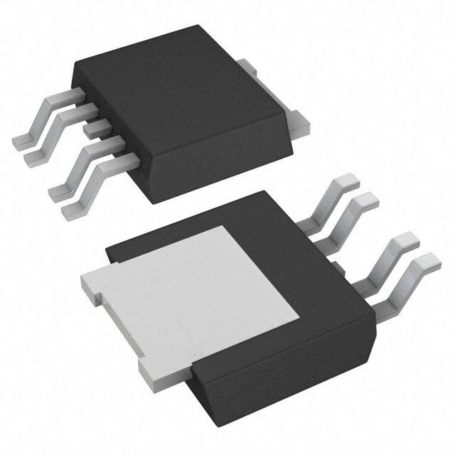
| 描述 | IC REG LDO 1.2V 1.5A PPAK低压差稳压器 1.5A Very Lo drop Vltg regulators |
| 产品分类 | |
| 品牌 | STMicroelectronics |
| 产品手册 | |
| 产品图片 |
|
| rohs | 符合RoHS无铅 / 符合限制有害物质指令(RoHS)规范要求 |
| 产品系列 | 电源管理 IC,低压差稳压器,STMicroelectronics LD49150PT12R- |
| 数据手册 | |
| 产品型号 | LD49150PT12R |
| 产品种类 | 低压差稳压器 |
| 供应商器件封装 | PPAK |
| 其它名称 | 497-6848-2 |
| 其它有关文件 | http://www.st.com/web/catalog/sense_power/FM142/CL1015/SC312/SS1733/PF173281?referrer=70071840 |
| 包装 | 带卷 (TR) |
| 参考电压 | 0.812 V |
| 商标 | STMicroelectronics |
| 回动电压—最大值 | 200 mV at 1.5 A |
| 安装类型 | 表面贴装 |
| 安装风格 | SMD/SMT |
| 封装 | Reel |
| 封装/外壳 | TO-252-5,DPak(4 引线 + 接片),TO-252AD |
| 封装/箱体 | PPAK-5 |
| 工作温度 | -25°C ~ 125°C |
| 工厂包装数量 | 2500 |
| 最大工作温度 | + 125 C |
| 最大输入电压 | 5.5 V |
| 最小工作温度 | - 25 C |
| 最小输入电压 | + 1.4 V |
| 标准包装 | 2,500 |
| 电压-跌落(典型值) | 1.5V @ 1.5A |
| 电压-输入 | 最高 5.5V |
| 电压-输出 | 1.2V |
| 电压调节准确度 | 1.5 % |
| 电流-输出 | 1.5A |
| 电流-限制(最小值) | 2.5A |
| 稳压器拓扑 | 正,固定式 |
| 稳压器数 | 1 |
| 系列 | LD49150XX12 |
| 线路调整率 | 0.1 % / V |
| 负载调节 | 1 % |
| 输出电压 | 800 mV to 4.5 V, 1.2 V |
| 输出电流 | 1.5 A |
| 输出端数量 | 1 Output |
| 输出类型 | Adjustable, Fixed |


PDF Datasheet 数据手册内容提取
LD49150 1.5 A ultra low-dropout voltage regulator Datasheet - production data Applications • Graphics processors • PC add-in cards • Microprocessor core voltage supply • Low voltage digital ICs • High efficiency linear power supplies PPAK DFN6 (3x3 mm) • SMPS post regulators Description Features The LD49150 is a high-bandwidth, low-dropout, • Input voltage range: 1.5 A voltage regulator, ideal for powering core – V = 1.4 V to 5.5 V voltages of low power microprocessors. The I LD49150 implements a dual supply configuration, – V = 3 V to 6 V BIAS which guarantees a very low output impedance • Stable with ceramic capacitors and a very fast transient response. The LD49150 • ±1.5% initial tolerance requires a bias input supply and a main input • Maximum dropout voltage (V - V ) 200 mV supply, allowing ultra-low input voltages on the I O main supply rail. The input supply operates from over the operating temperature range 1.4 V to 5.5 V and the bias supply requires • Adjustable output voltage starting from 0.8 V between 3 V and 6 V to work properly. The • Fast transient response (up to 10 MHz LD49150 offers fixed output voltages from 0.8 V to bandwidth) 1.8 V and adjustable output voltages starting from • Excellent line and load regulation 0.8 V. The LD49150 requires a minimum output capacitance for stability, and works optimally with specifications small ceramic capacitors. • Logic-controlled shutdown option • Thermal shutdown and current limit protection • Junction temperature range: - 25 °C to 125 °C Table 1. Device summary Order codes Output voltages PPAK (tape and reel) DFN6 (tape and reel) (1) LD49150PT08R Adjustable from 0.8 V LD49150PT10R LD49150PU10R 1.0 V LD49150PT12R LD49150PU12R 1.2 V 1. Available on request. May 2014 DocID13446 Rev 4 1/24 This is information on a product in full production. www.st.com
Contents LD49150 Contents 1 Typical application circuits . . . . . . . . . . . . . . . . . . . . . . . . . . . . . . . . . . . 3 2 Alternative application circuits . . . . . . . . . . . . . . . . . . . . . . . . . . . . . . . . 4 3 Pin configuration . . . . . . . . . . . . . . . . . . . . . . . . . . . . . . . . . . . . . . . . . . . 5 4 Diagram . . . . . . . . . . . . . . . . . . . . . . . . . . . . . . . . . . . . . . . . . . . . . . . . . . . 6 5 Maximum ratings . . . . . . . . . . . . . . . . . . . . . . . . . . . . . . . . . . . . . . . . . . . . 7 6 Electrical characteristics . . . . . . . . . . . . . . . . . . . . . . . . . . . . . . . . . . . . . 8 7 Typical characteristics . . . . . . . . . . . . . . . . . . . . . . . . . . . . . . . . . . . . . . . 9 8 Application hints . . . . . . . . . . . . . . . . . . . . . . . . . . . . . . . . . . . . . . . . . . . 12 8.1 Input supply voltage (VIN) . . . . . . . . . . . . . . . . . . . . . . . . . . . . . . . . . . . . 12 8.2 Bias supply voltage (VBIAS) . . . . . . . . . . . . . . . . . . . . . . . . . . . . . . . . . . 12 8.3 External capacitors . . . . . . . . . . . . . . . . . . . . . . . . . . . . . . . . . . . . . . . . . . 12 8.4 Output capacitor . . . . . . . . . . . . . . . . . . . . . . . . . . . . . . . . . . . . . . . . . . . . 12 8.5 Minimum load current . . . . . . . . . . . . . . . . . . . . . . . . . . . . . . . . . . . . . . . . 12 8.6 Power sequencing recommendations . . . . . . . . . . . . . . . . . . . . . . . . . . . 13 8.7 Power dissipation/heatsinking . . . . . . . . . . . . . . . . . . . . . . . . . . . . . . . . . 13 8.8 PPAK package heatsinking . . . . . . . . . . . . . . . . . . . . . . . . . . . . . . . . . . . 14 8.9 Adjustable regulator design . . . . . . . . . . . . . . . . . . . . . . . . . . . . . . . . . . . 14 8.10 Enable . . . . . . . . . . . . . . . . . . . . . . . . . . . . . . . . . . . . . . . . . . . . . . . . . . . 15 9 Package mechanical data . . . . . . . . . . . . . . . . . . . . . . . . . . . . . . . . . . . . 16 10 Packaging mechanical data . . . . . . . . . . . . . . . . . . . . . . . . . . . . . . . . . . 21 11 Revision history . . . . . . . . . . . . . . . . . . . . . . . . . . . . . . . . . . . . . . . . . . . 23 2/24 DocID13446 Rev 4
LD49150 Typical application circuits 1 Typical application circuits Figure 1. Adjustable version Figure 2. Fixed version with enable DocID13446 Rev 4 3/24 24
Alternative application circuits LD49150 2 Alternative application circuits Figure 3. Single supply voltage solution Figure 4. LD49150 and DC-DC pre-regulator to reduce power dissipation 4/24 DocID13446 Rev 4
LD49150 Pin configuration 3 Pin configuration Figure 5. Pin connections (PPAK top view, DFN bottom view) DFN6 (3x3 mm) PPAK Table 2. Pin description PPAK pin DFN pin Symbol Note EN Enable (input): logic high = enable, logic low = shutdown 1 2 ADJ Adjustable regulator feedback input connected to resistor voltage divider 2 3 V Input of the voltage regulator IN 3 1 GND Ground (tab is connected to ground) 4 4 V Regulator output OUT Input bias voltage powers circuitry on the regulator with the exception of the 5 6 V BIAS output power device 5 N.C. Not connected DocID13446 Rev 4 5/24 24
Diagram LD49150 4 Diagram Figure 6. Block diagram 6/24 DocID13446 Rev 4
LD49150 Maximum ratings 5 Maximum ratings Table 3. Absolute maximum ratings(1) Symbol Parameter Value Unit V Supply voltage -0.3 to 7 V IN -0.3 to V + 0.3 V Output voltage IN V OUT -0.3 to V + 0.3 BIAS V Bias supply voltage -0.3 to 7 V BIAS V Enable input voltage -0.3 to 7 V EN P Power dissipation Internally limited D T Storage temperature range -50 to 150 °C STG 1. All values are referred to ground. Note: Absolute maximum ratings are those values beyond which damage to the device may occur. Functional operation under these conditions is not implied. Table 4. Operating ratings Symbol Parameter Value Unit V Supply voltage 1.4 to 5.5 V IN V Output voltage 0.8 to 4.5 V OUT V Bias supply voltage 3 to 6 V BIAS V Enable input voltage 0 to V V EN BIAS T Junction temperature range -25 to 125 °C J DocID13446 Rev 4 7/24 24
Electrical characteristics LD49150 6 Electrical characteristics T = - 25 °C to 125 °C; V = V + 2.1 V (1); V = V +1 V; V = V (2); I = 10 mA; J BIAS O I O EN BIAS O C =1 µF; C = 10 µF; C = 1 µF; unless otherwise specified. Typical values refer to I O BIAS T =25 °C. J Table 5. Electrical characteristics Symbol Parameter Test conditions Min. Typ. Max. Unit T = 25 °C, fixed voltage option -1.5 1.5 J V Output voltage accuracy % O T = -25 °C to 125 °C -3 3 J V Line regulation V = V + 1 V to 5.5 V -0.1 0.1 %/V LINE I O V Load regulation I = 0 mA to 1.5 A, V ≥ 3 V 1 % LOAD L BIAS V Dropout voltage (V - V ) I = 1.5 A 200 mV DROP I O L V Dropout voltage (V - V ) I = 1.5 A(1) 1.5 2.1 V DROP BIAS O L I = 0 mA 4 6 L I Ground pin current mA GND I = 1.5 A 4 6 L I Ground pin current in shutdown V ≤ 0.4 V(2) 5 µA GND_SHD EN I = 0 mA 3 5 L I Current through V mA VBIAS BIAS I = 1.5 A 3 5 L I Current limit V = 0 V 2.5 A L O Enable input(2) Enable input threshold (fixed Regulator enable 1.4 V V EN voltage only) Regulator shutdown 0.4 I Enable pin input current 0.1 1 µA EN Reference T = 25 °C 0.788 0.8 0.812 J V Reference voltage V REF T = -25 °C to 125 °C 0.776 0.8 0.824 J V = 2.5 V ± 0.5 V, V = 1 V, SVR Supply voltage rejection I O 68 dB F = 120 Hz, V = 3.3 V BIAS 1. For V ≤ 1 V, V dropout specification is not applied due to 3 V minimum V input. O BIAS BIAS 2. Fixed output voltage version only. 8/24 DocID13446 Rev 4
LD49150 Typical characteristics 7 Typical characteristics Figure 7. Reference voltage vs. temperature Figure 8. Output voltage vs. temperature Figure 9. Load regulation vs. temperature Figure 10. Line regulation vs. temperature (cid:18)(cid:15)(cid:22)(cid:34) Figure 11. Output voltage vs. input voltage Figure 12. Dropout voltage (V -V ) vs. IN OUT temperature (cid:40)(cid:3)(cid:11)(cid:57)(cid:12) (cid:80)(cid:57)(cid:12) (cid:36)(cid:42) (cid:40)(cid:3)(cid:11) (cid:55) (cid:42) (cid:50)(cid:47) (cid:55)(cid:36) (cid:57) (cid:47) (cid:51)(cid:56)(cid:55)(cid:3) (cid:55)(cid:3)(cid:57)(cid:50) (cid:55) (cid:56) (cid:56) (cid:51) (cid:50) (cid:55) (cid:56) (cid:50) (cid:44)(cid:49)(cid:55)(cid:51)(cid:56)(cid:55)(cid:3)(cid:57)(cid:50)(cid:47)(cid:55)(cid:36)(cid:42)(cid:40)(cid:3)(cid:11)(cid:57)(cid:12) (cid:55)(cid:40)(cid:48)(cid:51)(cid:40)(cid:53)(cid:36)(cid:55)(cid:56)(cid:53)(cid:40)(cid:3)(cid:11)(cid:2195)(cid:131)(cid:38)(cid:12) DocID13446 Rev 4 9/24 24
Typical characteristics LD49150 Figure 13. V pin current vs. temperature Figure 14. Noise vs. frequency BIAS (cid:18)(cid:15)(cid:22)(cid:34) Figure 15. Quiescent current vs. temperature Figure 16. Supply voltage rejection vs. output current Figure 17. Stability region vs. C and high Figure 18. Stable region vs. C and low ESR OUT OUT ESR 10/24 DocID13446 Rev 4
LD49150 Typical characteristics Figure 19. V and V start-up transient Figure 20. V start-up transient response BIAS IN IN response(V andV startupatthe (V startup before than V ) T = 300 μs IN BIAS BIAS IN rise sametime) VIN=VBIAS=VEN=3.1V, VOUT=1V, COUT=1µF VIN=2.5V, VBIAS=VEN=3.1V, VOUT=1V, COUT=1µF Figure 21. V start-up transient response Figure 22. V start-up transient response IN IN (V startup before than V ) T = 30 μs (V startup before than V and V =V ) BIAS IN rise BIAS IN EN IN V =2.5V, V =V =3.1V, V =1V, C =1µF V =V =2.5V, V =3.1V, V =1V, C =1µF IN BIAS EN OUT OUT IN EN BIAS OUT OUT DocID13446 Rev 4 11/24 24
Application hints LD49150 8 Application hints The LD49150 is a low-dropout linear regulator, designed for high-current applications requiring a fast transient response. The LD49150 has separate input and bias voltage ports, in order to reduce dropout voltage. Thanks to the LD49150, a minimum quantity of external components is required. 8.1 Input supply voltage (V ) IN V provides the LD49150 with power input current. The minimum input voltage can be as IN low as 1.4 V, allowing conversion from very low voltage supplies to achieve low output voltage levels and low power dissipation. 8.2 Bias supply voltage (V ) BIAS The LD49150 control circuitry is supplied by V pin, which requires a very low bias BIAS current (3 mA typ.) even at the maximum output current level (1.5 A). A bypass capacitor on V pin improves the LD49150 performance during line and load transient. The small BIAS ceramic capacitor from V to ground reduces high frequency noise that could be injected BIAS into the control circuitry. In typical applications, one ceramic chip capacitor of 1 µF may be used. V input voltage has to be 2.1 V above the output voltage, with a minimum V BIAS BIAS input voltage of 3 V. 8.3 External capacitors To assure regulator stability, input and output capacitors are required as shown in Section1. 8.4 Output capacitor The LD49150 requires a minimum output capacitance to maintain stability. At least 1 µF ceramic chip capacitor is required. However, a specific capacitor selection assures the transient response. 1 µF ceramic chip capacitor satisfies most applications but 10 µF guarantees a better transient performance. In applications where V level is close to the IN maximum operating voltage (V > 4 V), a minimum 10 µF output capacitor avoids IN overvoltage stress on the input/output power pins during short-circuit conditions due to parasitic inductive effect. The output capacitor has to be as closer as possible to the LD49150 output pin. ESR output capacitor (equivalent series resistance) has to be within the stable region as shown in Section7. Both ceramic and tantalum capacitors are suitable. 8.5 Minimum load current The LD49150 does not require a minimum load to maintain the output voltage regulation. 12/24 DocID13446 Rev 4
LD49150 Application hints 8.6 Power sequencing recommendations To assure the correct biasing and settling of the regulator internal circuitry during the start- up phase, and to avoid overvoltage spikes on the output, the correct power sequencing has to be provided. As general rule, V and V signal timings should be chosen properly, so that they are IN INH applied to the device after V voltage has already been settled on its minimum operative BIAS value (see Section8.2). This can be achieved, for instance, by avoiding too slow V BIAS rising edges (T >10 ms). r Provided that the above condition is satisfied, when fast V transient input (T < 100 µs) is IN r present, a smooth startup, with limited overvoltage on the output, can be achieved by V IN and V voltage simultaneously (refer to Figure20, Figure21 and Figure22). BIAS In the fixed voltage version, overvoltage spikes can be reduced during very fast startup (T r << 100 µs) by pulling V pin up to V voltage (see Figure23). EN IN 8.7 Power dissipation/heatsinking In relation to the maximum power dissipation and maximum ambient temperature of the application, a heatsink may be required. Junction temperature has to be within the specified range under operating conditions. The total power dissipation of the device is given by: Equation 1 P = V x I + V x I - V x I D IN IN BIAS BIAS OUT OUT where: • V = input supply voltage IN • V = bias supply voltage BIAS • V = output voltage OUT • I = load current OUT θ The required thermal resistance for the heatsink is given by the following formula: SA Equation 2 θ θ θ = (T - T /P ) - ( + ) SA J A D JC CS T , the maximum allowed temperature rise depends on T , the maximum ambient Rmax Amax temperature of the application, and T , the maximum allowable junction temperature: Jmax Equation 3 T = T - T Rmax Jmax Amax θ , the maximum allowable value for junction-to-ambient thermal resistance can be JA calculated as follows: Equation 4 θ = T / P JAmax Rmax D The thermal resistance depends on the amount of copper area or heatsink, and on the air flow. If θ the maximum allowable value is ≥ 100 °C/W for the PPAK package, no heatsink is JA DocID13446 Rev 4 13/24 24
Application hints LD49150 needed since the package can dissipate enough heat to satisfy these requirements. If the θ allowable value falls below these limits, a heatsink is required as described below. JA 8.8 PPAK package heatsinking The PPAK package uses the copper plane on the PCB as a heatsink. The tab of this package is soldered onto the copper plane for the heatsinking. PCB ground plane can be used as a heatsink. This area can be the inner GND layer of a multi-layer PCB, or, in a dual- layer PCB, it can be an unbroken GND area on the bottom layer, thermally connected to the tab through-via holes. θ Figure23 shows curve for PPAK package for different copper area sizes, using a typical JA PCB: thickness 1/16 G10 FR4. θ Figure 23. vs. copper area for PPAK package JA 8.9 Adjustable regulator design The LD49150 adjustable version allows the output voltage to be fixed anywhere between 0.8 V and 4.5 V using two resistors as shown in the typical application circuit. For example, to fix R resistor value between V and ADJ pin, the resistor value between ADJ and 1 OUT GND (R ) is calculated as follows: 2 R = R [0.8/(V - 0.8)] 2 1 OUT where V is the desired output voltage. OUT R values should be lower than 10 kΩ to obtain a better load transient performance. Higher 1 values up to 100 kΩ are suitable. 14/24 DocID13446 Rev 4
LD49150 Application hints 8.10 Enable The LD49150 fixed output voltage version features an active high enable input (EN) that allows the on-off control of the regulator. EN input threshold is guaranteed between 0.4 V and 1.4 V. The regulator is in shutdown mode when V < 0.4 V and it is in operating mode EN (V activated) when V > 1.4 V. If it is not in use, EN pin has to be tied directly to V to OUT EN IN keep the regulator continuously activated. En pin has not to be left with high impedance. DocID13446 Rev 4 15/24 24
Package mechanical data LD49150 9 Package mechanical data In order to meet environmental requirements, ST offers these devices in different grades of ECOPACK® packages, depending on their level of environmental compliance. ECOPACK® specifications, grade definitions and product status are available at: www.st.com. ECOPACK® is an ST trademark. 16/24 DocID13446 Rev 4
LD49150 Package mechanical data Figure 24. PPAK drawing 0078180_F DocID13446 Rev 4 17/24 24
Package mechanical data LD49150 Table 6. PPAK mechanical data mm Dim. Min. Typ. Max. A 2.2 2.4 A1 0.9 1.1 A2 0.03 0.23 B 0.4 0.6 B2 5.2 5.4 C 0.45 0.6 C2 0.48 0.6 D 6 6.2 D1 5.1 E 6.4 6.6 E1 4.7 e 1.27 G 4.9 5.25 G1 2.38 2.7 H 9.35 10.1 L2 0.8 1 L4 0.6 1 L5 1 L6 2.8 R 0.20 V2 0° 8° 18/24 DocID13446 Rev 4
LD49150 Package mechanical data Figure 25. DFN6 (3x3 mm) drawing (cid:26)(cid:28)(cid:23)(cid:25)(cid:25)(cid:22)(cid:26)(cid:66)(cid:38) DocID13446 Rev 4 19/24 24
Package mechanical data LD49150 Table 7. DFN6 (3x3 mm) mechanical data mm Dim. Min. Typ. Max. A 0.80 1 A1 0 0.02 0.05 A3 0.20 b 0.23 0.45 D 2.90 3 3.10 D2 2.23 2.50 E 2.90 3 3.10 E2 1.50 1.75 e 0.95 L 0.30 0.40 0.50 Figure 26. DFN6 (3x3 mm) footprint recommended data 20/24 DocID13446 Rev 4
LD49150 Packaging mechanical data 10 Packaging mechanical data Figure 27. DFN6 (3x3 mm) tape (cid:26)(cid:27)(cid:26)(cid:24)(cid:28)(cid:26)(cid:27)(cid:66)(cid:49) DocID13446 Rev 4 21/24 24
Packaging mechanical data LD49150 Figure 28. DFN6 (3x3 mm) reel (cid:26)(cid:27)(cid:26)(cid:24)(cid:28)(cid:26)(cid:27)(cid:66)(cid:49) Table 8. DFN6 (3x3 mm) tape and reel mechanical data mm Dim. Min. Typ. Max. A0 3.20 3.30 3.40 B0 3.20 3.30 3.40 K0 1 1.10 1.20 22/24 DocID13446 Rev 4
LD49150 Revision history 11 Revision history Table 9. Document revision history Date Revision Changes 18-Apr-2007 1 Initial release. 12-Jan-2009 2 Added new package DFN6 (3x3 mm) and mechanical data. Modified Section8.6: Power sequencing recommendations on 29-Jun-2010 3 page13. Changed the part numbers LD49150xx08, LD49150xx10 and LD49150xx12 to LD49150. Changed the title. Updated the description in cover page, Table1: Device summary, 26-May-2014 4 Section7: Typical characteristics, Section8: Application hints, Section9: Package mechanical data. Added Section10: Packaging mechanical data. Minor text changes. DocID13446 Rev 4 23/24 24
LD49150 Please Read Carefully: Information in this document is provided solely in connection with ST products. STMicroelectronics NV and its subsidiaries (“ST”) reserve the right to make changes, corrections, modifications or improvements, to this document, and the products and services described herein at any time, without notice. All ST products are sold pursuant to ST’s terms and conditions of sale. Purchasers are solely responsible for the choice, selection and use of the ST products and services described herein, and ST assumes no liability whatsoever relating to the choice, selection or use of the ST products and services described herein. No license, express or implied, by estoppel or otherwise, to any intellectual property rights is granted under this document. If any part of this document refers to any third party products or services it shall not be deemed a license grant by ST for the use of such third party products or services, or any intellectual property contained therein or considered as a warranty covering the use in any manner whatsoever of such third party products or services or any intellectual property contained therein. UNLESS OTHERWISE SET FORTH IN ST’S TERMS AND CONDITIONS OF SALE ST DISCLAIMS ANY EXPRESS OR IMPLIED WARRANTY WITH RESPECT TO THE USE AND/OR SALE OF ST PRODUCTS INCLUDING WITHOUT LIMITATION IMPLIED WARRANTIES OF MERCHANTABILITY, FITNESS FOR A PARTICULAR PURPOSE (AND THEIR EQUIVALENTS UNDER THE LAWS OF ANY JURISDICTION), OR INFRINGEMENT OF ANY PATENT, COPYRIGHT OR OTHER INTELLECTUAL PROPERTY RIGHT. ST PRODUCTS ARE NOT DESIGNED OR AUTHORIZED FOR USE IN: (A) SAFETY CRITICAL APPLICATIONS SUCH AS LIFE SUPPORTING, ACTIVE IMPLANTED DEVICES OR SYSTEMS WITH PRODUCT FUNCTIONAL SAFETY REQUIREMENTS; (B) AERONAUTIC APPLICATIONS; (C) AUTOMOTIVE APPLICATIONS OR ENVIRONMENTS, AND/OR (D) AEROSPACE APPLICATIONS OR ENVIRONMENTS. WHERE ST PRODUCTS ARE NOT DESIGNED FOR SUCH USE, THE PURCHASER SHALL USE PRODUCTS AT PURCHASER’S SOLE RISK, EVEN IF ST HAS BEEN INFORMED IN WRITING OF SUCH USAGE, UNLESS A PRODUCT IS EXPRESSLY DESIGNATED BY ST AS BEING INTENDED FOR “AUTOMOTIVE, AUTOMOTIVE SAFETY OR MEDICAL” INDUSTRY DOMAINS ACCORDING TO ST PRODUCT DESIGN SPECIFICATIONS. PRODUCTS FORMALLY ESCC, QML OR JAN QUALIFIED ARE DEEMED SUITABLE FOR USE IN AEROSPACE BY THE CORRESPONDING GOVERNMENTAL AGENCY. Resale of ST products with provisions different from the statements and/or technical features set forth in this document shall immediately void any warranty granted by ST for the ST product or service described herein and shall not create or extend in any manner whatsoever, any liability of ST. ST and the ST logo are trademarks or registered trademarks of ST in various countries. Information in this document supersedes and replaces all information previously supplied. The ST logo is a registered trademark of STMicroelectronics. All other names are the property of their respective owners. © 2014 STMicroelectronics - All rights reserved STMicroelectronics group of companies Australia - Belgium - Brazil - Canada - China - Czech Republic - Finland - France - Germany - Hong Kong - India - Israel - Italy - Japan - Malaysia - Malta - Morocco - Philippines - Singapore - Spain - Sweden - Switzerland - United Kingdom - United States of America www.st.com 24/24 DocID13446 Rev 4
Mouser Electronics Authorized Distributor Click to View Pricing, Inventory, Delivery & Lifecycle Information: S TMicroelectronics: LD49150PT12R LD49150PT08R LD49150PT10R