ICGOO在线商城 > LD29080PT25R
 Datasheet下载
- 型号: LD29080PT25R
- 制造商: STMicroelectronics
- 库位|库存: xxxx|xxxx
- 要求:
| 数量阶梯 | 香港交货 | 国内含税 |
| +xxxx | $xxxx | ¥xxxx |
查看当月历史价格
查看今年历史价格
LD29080PT25R产品简介:
ICGOO电子元器件商城为您提供LD29080PT25R由STMicroelectronics设计生产,在icgoo商城现货销售,并且可以通过原厂、代理商等渠道进行代购。 提供LD29080PT25R价格参考¥3.03-¥3.03以及STMicroelectronicsLD29080PT25R封装/规格参数等产品信息。 你可以下载LD29080PT25R参考资料、Datasheet数据手册功能说明书, 资料中有LD29080PT25R详细功能的应用电路图电压和使用方法及教程。
| 参数 | 数值 |
| 产品目录 | 集成电路 (IC)半导体 |
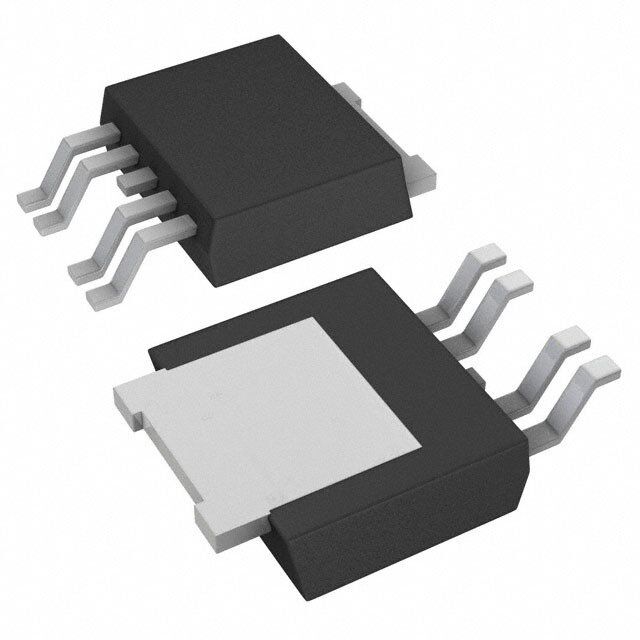
| 描述 | IC REG LDO 2.5V 0.8A PPAK低压差稳压器 800mA Fixed Adjust output very Lo drop |
| 产品分类 | |
| 品牌 | STMicroelectronics |
| 产品手册 | |
| 产品图片 |
|
| rohs | 符合RoHS无铅 / 符合限制有害物质指令(RoHS)规范要求 |
| 产品系列 | 电源管理 IC,低压差稳压器,STMicroelectronics LD29080PT25R- |
| 数据手册 | |
| 产品型号 | LD29080PT25R |
| 产品种类 | 低压差稳压器 |
| 供应商器件封装 | PPAK |
| 包装 | 带卷 (TR) |
| 商标 | STMicroelectronics |
| 回动电压—最大值 | 700 mV at 800 mA |
| 安装类型 | 表面贴装 |
| 安装风格 | SMD/SMT |
| 封装 | Reel |
| 封装/外壳 | TO-252-5,DPak(4 引线 + 接片),TO-252AD |
| 封装/箱体 | PPAK-5 |
| 工作温度 | -40°C ~ 125°C |
| 工厂包装数量 | 2500 |
| 最大工作温度 | + 125 C |
| 最大输入电压 | 13 V |
| 最小工作温度 | - 40 C |
| 最小输入电压 | + 2.5 V |
| 标准包装 | 2,500 |
| 电压-跌落(典型值) | 0.4V @ 800mA |
| 电压-输入 | 最高 13V |
| 电压-输出 | 2.5V |
| 电压调节准确度 | 1 % |
| 电流-输出 | 800mA |
| 电流-限制(最小值) | - |
| 稳压器拓扑 | 正,固定式 |
| 稳压器数 | 1 |
| 系列 | LD29080 |
| 线路调整率 | 0.5 % |
| 负载调节 | 1 % |
| 输入偏压电流—最大 | 2 mA |
| 输出电压 | 2.5 V |
| 输出电流 | 800 mA |
| 输出端数量 | 1 Output |
| 输出类型 | Fixed |


- 商务部:美国ITC正式对集成电路等产品启动337调查
- 曝三星4nm工艺存在良率问题 高通将骁龙8 Gen1或转产台积电
- 太阳诱电将投资9.5亿元在常州建新厂生产MLCC 预计2023年完工
- 英特尔发布欧洲新工厂建设计划 深化IDM 2.0 战略
- 台积电先进制程称霸业界 有大客户加持明年业绩稳了
- 达到5530亿美元!SIA预计今年全球半导体销售额将创下新高
- 英特尔拟将自动驾驶子公司Mobileye上市 估值或超500亿美元
- 三星加码芯片和SET,合并消费电子和移动部门,撤换高东真等 CEO
- 三星电子宣布重大人事变动 还合并消费电子和移动部门
- 海关总署:前11个月进口集成电路产品价值2.52万亿元 增长14.8%


PDF Datasheet 数据手册内容提取
LD29080 800 mA fixed and adjustable output very low drop voltage regulator Datasheet - production data Description The LD29080 is a medium current, high accuracy, low-dropout voltage regulators series. These regulators feature 400 mV dropout voltage and very low ground current. Designed for medium current loads, these devices also find applications PPAK DPAK in lower current, extremely low dropout-critical systems, where their tiny dropout voltage and ground current values are important attributes. Typical application are in power supply switching post regulation, series power supply for monitors, SOT223 series power supply for VCRs and TVs, computer systems and battery powered systems. Features • Very low dropout voltage (typ. 0.4 at 800 mA) • Guaranteed output current up to 800 mA • Fixed and adjustable output voltage (± 1 % at 25 °C) • Internal current and thermal limit • Logic controlled electronic shutdown Table 1. Device summary Order codes Output voltages DPAK (tape and reel) PPAK (tape and reel) SOT223 LD29080DT15R LD29080PT15R 1.5 V LD29080DT18R LD29080PT18R 1.8 V LD29080DT25R LD29080PT25R 2.5 V LD29080DT33R LD29080PT33R LD29080S33R 3.3 V LD29080DT50R LD29080PT50R 5.0 V LD29080DT90R LD29080PT90R 9.0 V LD29080PTR ADJ February 2020 DocID10918 Rev 9 1/26 This is information on a product in full production. www.st.com 26
Contents LD29080 Contents 1 Diagram . . . . . . . . . . . . . . . . . . . . . . . . . . . . . . . . . . . . . . . . . . . . . . . . . . . 3 2 Pin configuration . . . . . . . . . . . . . . . . . . . . . . . . . . . . . . . . . . . . . . . . . . . 4 3 Maximum ratings . . . . . . . . . . . . . . . . . . . . . . . . . . . . . . . . . . . . . . . . . . . . 5 4 Electrical characteristics . . . . . . . . . . . . . . . . . . . . . . . . . . . . . . . . . . . . . 6 5 Typical characteristics . . . . . . . . . . . . . . . . . . . . . . . . . . . . . . . . . . . . . . 14 6 Package mechanical data . . . . . . . . . . . . . . . . . . . . . . . . . . . . . . . . . . . . 17 7 Packaging mechanical data . . . . . . . . . . . . . . . . . . . . . . . . . . . . . . . . . . 23 8 Revision history . . . . . . . . . . . . . . . . . . . . . . . . . . . . . . . . . . . . . . . . . . . 25 2/26 DocID10918 Rev 9
LD29080 Diagram 1 Diagram Figure 1. Schematic diagram for adjustable version Figure 2. Schematic diagram for fixed version * Only for version with inhibit function. DocID10918 Rev 9 3/26
Pin configuration LD29080 2 Pin configuration Figure 3. Pin connections (top view) 5 3 4 GND GND 3 GND 2 2 1 1 1 2 3 CS17230 CS17240 AM09358v1 PPAK DPAK SOT223 Table 2. Pin description Symbol PPAK DPAK SOT223 V 2 1 1 I GND 3 2 2 V 4 3 3 O ADJ/N.C. (1) 5 INHIBIT (2) 1 1. Not connected for fixed version. 2. Not internally pulled up; in order to assure the operating condition (device in ON mode), it must be connected to a positive voltage higher than 2 V. Figure 4. Application circuit V = V (1 + R /R ) O REF 1 2 * Only for version with inhibit function. 4/26 DocID10918 Rev 9
LD29080 Maximum ratings 3 Maximum ratings Table 3. Absolute maximum ratings Symbol Parameter Value Unit V DC input voltage 30 (1) V I V Inhibit input voltage 14 V INH I Output current Internally limited mA O P Power dissipation Internally limited mW D T Storage temperature range - 55 to 150 °C STG T Operating temperature range - 40 to 125 °C OP 1. Above 14 V the device is automatically in shut-down. Note: Absolute maximum ratings are those values beyond which damage to the device may occur. Functional operation under these conditions is not implied. Table 4. Thermal data Symbol Parameter DPAK PPAK SOT223 Unit R Thermal resistance junction-case 8 8 25 °C/W thJC R Thermal resistance junction-ambient 100 100 110 °C/W thJA DocID10918 Rev 9 5/26
Electrical characteristics LD29080 4 Electrical characteristics I = 10 mA, (Note4) T = 25 °C, V = 3.5 V, V = 2V, C = 330 nF, C = 10 µF, unless O J I INH I O otherwise specified. Table 5. Electrical characteristics of LD29080#15 Symbol Parameter Test conditions Min. Typ. Max. Unit V Operating input voltage I = 10 mA to 800 mA 2.5 13 V I O I = 10 mA to 800 mA, V = 3 to 7 V 1.485 1.5 1.515 V Output voltage O I V O TJ = -40 to 125 °C 1.463 1.537 D V Load regulation I = 10 mA to 800 mA 0.2 1.0 % O O D V Line regulation V = 3 to 13 V 0.06 0.5 % O I f = 120 Hz, V = 3.8 – 1 V, I = 400 mA SVR Supply voltage rejection I O 65 75 dB (Note1) I = 10 mA, T = -40 to 125 °C 2 5 O J I = 400 mA, T = -40 to 125 °C 8 20 mA O J I Quiescent current q I = 800 mA, T = -40 to 125 °C 14 35 O J V = 13 V, V = GND, T = -40 to 125 °C 130 180 µA I INH J I Short circuit current R = 0 1.2 A sc L V Control input logic low OFF MODE, T = -40 to 125 °C 0.8 V IL J V Control input logic high ON MODE, T = -40 to 125 °C 2 V IH J I Control input current V = 13V, T = -40 to 125 °C 5 10 µA INH INH J B = 10 Hz to 100 kHz, I = 100 mA eN Output noise voltage P O 60 µV (Note1) RMS Note: 1 Guaranteed by design. 2 Dropout voltage is defined as the input-to-output differential when the output voltage drops to 99% of its nominal value with V + 1 V applied to V. O I 3 Reference voltage is measured between output and GND pins, with ADJ PIN tied to V . O 4 In order to avoid any output voltage rise within the whole operating temperature range, due to output leakage current, a minimum load current of 2 mA is required. 6/26 DocID10918 Rev 9
LD29080 Electrical characteristics I = 10 mA, (Note4) T = 25 °C, V = 3.5 V, V = 2 V, C = 330 nF, C = 10 µF, unless O J I INH I O otherwise specified. Table 6. Electrical characteristics of LD29080#18 Symbol Parameter Test conditions Min. Typ. Max. Unit V Operating input voltage I = 10 mA to 800 mA 2.5 13 V I O I = 10 mA to 800 mA, V = 3 to 7.3 V 1.782 1.8 1.818 V Output voltage O I V O TJ = -40 to 125 °C 1.755 1.845 D V Load regulation I = 10 mA to 800 mA 0.2 1.0 % O O D V Line regulation V = 3 to 13 V 0.06 0.5 % O I f = 120 Hz, V = 3.8 – 1 V, I = 400 mA SVR Supply voltage rejection I O 62 72 dB (Note1) I = 150 mA, T = -40 to 125 °C (Note2) 0.1 O J V Dropout voltage I = 400 mA, T = -40 to 125 °C (Note2) 0.2 V DROP O J I = 800 mA, T = -40 to 125 °C (Note2) 0.4 0.7 O J I = 10 mA, T = -40 to 125 °C 2 5 O J I = 400 mA, T = -40 to 125 °C 8 20 mA O J I Quiescent current q I = 800 mA, T = -40 to 125 °C 14 35 O J V = 13 V, V = GND, T = -40 to 125 °C 130 180 µA I INH J I Short circuit current R = 0 1.2 A sc L V Control input logic low OFF MODE, T = -40 to 125 °C 0.8 V IL J V Control input logic high ON MODE, T = -40 to 125 °C 2 V IH J I Control input current V = 13 V, T = -40 to 125 °C 5 10 µA INH INH J B = 10 Hz to 100 kHz, I = 100 mA eN Output noise voltage P O 72 µV (Note1) RMS Note: 1 Guaranteed by design. 2 Dropout voltage is defined as the input-to-output differential when the output voltage drops to 99% of its nominal value with V + 1 V applied to V. O I 3 Reference voltage is measured between output and GND pins, with ADJ PIN tied to V . O 4 In order to avoid any output voltage rise within the whole operating temperature range, due to output leakage current, a minimum load current of 2 mA is required. DocID10918 Rev 9 7/26
Electrical characteristics LD29080 I = 10 mA, (Note4) T = 25 °C, V = 4.5 V, V = 2 V, C = 330 nF, C = 10 µF, unless O J I INH I O otherwise specified. Table 7. Electrical characteristics of LD29080#25 Symbol Parameter Test conditions Min. Typ. Max. Unit V Operating input voltage I = 10 mA to 800 mA 13 V I O I = 10 mA to 800 mA, V = 3.5 to 8 V 2.475 2.5 2.525 V Output voltage O I V O TJ = -40 to 125 °C 2.438 2.562 D V Load regulation I = 10 mA to 800 mA 0.2 1.0 % O O D V Line regulation V = 3.5 to 13 V 0.06 0.5 % O I f = 120 Hz, V = 4.5 – 1 V, I = 400 mA SVR Supply voltage rejection I O 55 70 dB (Note1) I = 150 mA, T = -40 to 125 °C (Note2) 0.1 O J V Dropout voltage I = 400 mA, T = -40 to 125 °C (Note2) 0.2 V DROP O J I = 800 mA, T = -40 to 125 °C (Note2) 0.4 0.7 O J I = 10 mA, T = -40 to 125 °C 2 5 O J I = 400 mA, T = -40 to 125 °C 8 20 mA O J I Quiescent current q I = 800 mA, T = -40 to 125 °C 14 35 O J V = 13 V, V = GND, T = -40 to 125 °C 130 180 µA I INH J I Short circuit current R = 0 1.2 A sc L V Control input logic low OFF MODE, T = -40 to 125 °C 0.8 V IL J V Control input logic high ON MODE, T = -40 to 125 °C 2 V IH J I Control input current V = 13 V, T = -40 to 125 °C 5 10 µA INH INH J B = 10 Hz to 100 kHz, I = 100 mA eN Output noise voltage P O 100 µV (Note1) RMS Note: 1 Guaranteed by design. 2 Dropout voltage is defined as the input-to-output differential when the output voltage drops to 99% of its nominal value with V + 1 V applied to V. O I 3 Reference voltage is measured between output and GND pins, with ADJ PIN tied to V . O 4 In order to avoid any output voltage rise within the whole operating temperature range, due to output leakage current, a minimum load current of 2 mA is required. 8/26 DocID10918 Rev 9
LD29080 Electrical characteristics I = 10 mA, (Note4) T = 25 °C, V = 5.3 V, V = 2 V, C = 330 nF, C = 10 µF, unless O J I INH I O otherwise specified. Table 8. Electrical characteristics of LD29080#33 Symbol Parameter Test conditions Min. Typ. Max. Unit V Operating input voltage I = 10mA to 800mA 13 V I O I = 10 mA to 800 mA, V = 4.3 to 8.8 V 3.267 3.3 3.333 V Output voltage O I V O TJ = -40 to 125 °C 3.218 3.382 D V Load regulation I = 10 mA to 800 mA 0.2 1.0 % O O D V Line regulation V = 4.3 to 13 V 0.06 0.5 % O I f = 120 Hz, V = 5.3 – 1 V, I = 400 mA SVR Supply voltage rejection I O 52 67 dB (Note1) I = 150 mA, T = -40 to 125 °C (Note2) 0.1 O J V Dropout voltage I = 400 mA, T = -40 to 125 °C (Note2) 0.2 V DROP O J I = 800 mA, T = -40 to 125 °C (Note2) 0.4 0.7 O J I = 10 mA, T = -40 to 125 °C 2 5 O J I = 400 mA, T = -40 to 125 °C 8 20 mA O J I Quiescent current q I = 800 mA, T = -40 to 125 °C 14 35 O J V = 13 V, V = GND, T = -40 to 125 °C 130 180 µA I INH J I Short circuit current R = 0 1.2 A sc L V Control input logic low OFF MODE, T = -40 to 125 °C 0.8 V IL J V Control input logic high ON MODE, T = -40 to 125 °C 2 V IH J I Control input current V = 13 V, T = -40 to 125 °C 5 10 µA INH INH J B = 10 Hz to 100 kHz, I = 100 mA eN Output noise voltage P O 132 µV (Note1) RMS Note: 1 Guaranteed by design. 2 Dropout voltage is defined as the input-to-output differential when the output voltage drops to 99% of its nominal value with V + 1 V applied to V. O I 3 Reference voltage is measured between output and GND pins, with ADJ PIN tied to V . O 4 In order to avoid any output voltage rise within the whole operating temperature range, due to output leakage current, a minimum load current of 2 mA is required. DocID10918 Rev 9 9/26
Electrical characteristics LD29080 I = 10 mA, (Note4) T = 25 °C, V = 7 V, V = 2 V, C = 330 nF, C = 10 µF, unless O J I INH I O otherwise specified. Table 9. Electrical characteristics of LD29080#50 Symbol Parameter Test conditions Min. Typ. Max. Unit V Operating input voltage I = 10 mA to 800 mA 13 V I O I = 10 mA to 800 mA, V = 6 to 10.5 V 4.95 5 5.05 V Output voltage O I V O TJ = -40 to 125 °C 4.875 5.125 D V Load regulation I = 10 mA to 800 mA 0.2 1.0 % O O D V Line regulation V = 6 to 13 V 0.06 0.5 % O I f = 120 Hz, V = 7 – 1 V, I = 400 mA SVR Supply voltage rejection I O 49 64 dB (Note1) I = 150 mA, T = -40 to 125 °C (Note2) 0.1 O J V Dropout voltage I = 400 mA, T = -40 to 125 °C (Note2) 0.2 V DROP O J I = 800 mA, T = -40 to 125 °C (Note2) 0.4 0.7 O J I = 10 mA, T = -40 to 125 °C 2 5 O J I = 400 mA, T = -40 to 125 °C 8 20 mA O J I Quiescent current q I = 800 mA, T = -40 to 125 °C 14 35 O J V = 13 V, V = GND, T = -40 to 125 °C 130 180 µA I INH J I Short circuit current R = 0 1.2 A sc L V Control input logic low OFF MODE, T = -40 to 125 °C 0.8 V IL J V Control input logic high ON MODE, T = -40 to 125 °C 2 V IH J I Control input current V = 13 V, T = -40 to 125 °C 5 10 µA INH INH J B = 10 Hz to 100 kHz, I = 100 mA eN Output noise voltage P O 180 µV (Note1) RMS Note: 1 Guaranteed by design. 2 Dropout voltage is defined as the input-to-output differential when the output voltage drops to 99% of its nominal value with V + 1 V applied to V. O I 3 Reference voltage is measured between output and GND pins, with ADJ PIN tied to V . O 4 In order to avoid any output voltage rise within the whole operating temperature range, due to output leakage current, a minimum load current of 2 mA is required. 10/26 DocID10918 Rev 9
LD29080 Electrical characteristics I = 10 mA, (Note4) T = 25 °C, V = 10 V, V = 2 V, C = 330 nF, C = 10 µF, unless O J I INH I O otherwise specified) Table 10. Electrical characteristics of LD29080#80 Symbol Parameter Test conditions Min. Typ. Max. Unit V Operating input voltage I = 10 mA to 800 mA 13 V I O I = 10 mA to 800 mA, V = 9 to 13 V 7.92 8 8.08 V Output voltage O I V O TJ = -40 to 125 °C 7.80 8.20 D V Load regulation I = 10 mA to 800 mA 0.2 1.0 % O O D V Line regulation V = 9 to 13 V 0.06 0.5 % O I f = 120 Hz, V = 10 – 1 V, I = 400 mA SVR Supply voltage rejection I O 45 59 dB (Note1) I = 150 mA, T = -40 to 125 °C (Note2) 0.1 O J V Dropout voltage I = 400 mA, T = -40 to 125 °C (Note2) 0.2 V DROP O J I = 800 mA, T = -40 to 125 °C (Note2) 0.4 0.7 O J I = 10 mA, T = -40 to 125 °C 2 5 O J I = 400 mA, T = -40 to 125 °C 8 20 mA O J I Quiescent current q I = 800 mA, T = -40 to 125 °C 14 35 O J V = 13 V, V = GND, T = -40 to 125 °C 130 180 µA I INH J I Short circuit current R = 0 1.2 A sc L V Control input logic low OFF MODE, T = -40 to 125 °C 0.8 V IL J V Control input logic high ON MODE, T = -40 to 125 °C 2 V IH J I Control input current V = 13 V, T = -40 to 125 °C 5 10 µA INH INH J B = 10 Hz to 100 kHz, I = 100 mA eN Output noise voltage P O 320 µV (Note1) RMS Note: 1 Guaranteed by design. 2 Dropout voltage is defined as the input-to-output differential when the output voltage drops to 99% of its nominal value with V + 1 V applied to V. O I 3 Reference voltage is measured between output and GND pins, with ADJ PIN tied to V . O 4 In order to avoid any output voltage rise within the whole operating temperature range, due to output leakage current, a minimum load current of 2 mA is required. DocID10918 Rev 9 11/26
Electrical characteristics LD29080 I = 10 mA, (Note4) T = 25 °C, V = 11 V, V = 2 V, C = 330 nF, C = 10 µF, unless O J I INH I O otherwise specified. Table 11. Electrical characteristics of LD29080#90 Symbol Parameter Test conditions Min. Typ. Max. Unit V Operating input voltage I = 10 mA to 800 mA 13 V I O I = 10 mA to 800 mA, V = 9 to 13 V 8.91 9 9.09 V Output voltage O I V O TJ = -40 to 125 °C 8.775 9.225 D V Load regulation I = 10 mA to 800 mA 0.2 1.0 % O O D V Line regulation V = 10 to 13 V 0.06 0.5 % O I f = 120 Hz, V = 11 – 1 V, I = 400 mA SVR Supply voltage rejection I O 43 57 dB (Note1) I = 150 mA, T = -40 to 125 °C (Note2) 0.1 O J V Dropout voltage I = 400 mA, T = -40 to 125 °C (Note2) 0.2 V DROP O J I = 800 mA, T = -40 to 125 °C (Note2) 0.4 0.7 O J I = 10 mA, T = -40 to 125 °C 2 5 O J I = 400 mA, T = -40 to 125 °C 8 20 mA O J I Quiescent current q I = 800 mA, T = -40 to 125 °C 14 35 O J V = 13 V, V = GND, T = -40 to 125 °C 130 180 µA I INH J I Short circuit current R = 0 1.2 A sc L V Control input logic low OFF MODE, T = -40 to 125 °C 0.8 V IL J V Control input logic high ON MODE, T = -40 to 125 °C 2 V IH J I Control input current V = 13 V, T = -40 to 125 °C 5 10 µA INH INH J B = 10 Hz to 100 kHz, I = 100 mA eN Output noise voltage P O 330 µV (Note1) RMS Note: 1 Guaranteed by design. 2 Dropout voltage is defined as the input-to-output differential when the output voltage drops to 99% of its nominal value with V + 1 V applied to V. O I 3 Reference voltage is measured between output and GND pins, with ADJ PIN tied to V . O 4 In order to avoid any output voltage rise within the whole operating temperature range, due to output leakage current, a minimum load current of 2 mA is required. 12/26 DocID10918 Rev 9
LD29080 Electrical characteristics I = 10 mA, (Note4) T = 25 °C, V = 10 V, V = 2 V, C = 330 nF, C = 10 µF, unless O J I INH I O otherwise specified. Table 12. Electrical characteristics of LD29080#ADJ Symbol Parameter Test conditions Min. Typ. Max. Unit V Operating input voltage I = 10 mA to 800 mA 2.5 13 V I O D V Load regulation I = 10 mA to 800 mA 0.2 1.0 % O O D V Line regulation V = 2.5 to 13 V, I = 10 mA 0.06 0.5 % O I O I = 10 mA to 800 mA, V = 2.5 to 6.73 V 1.2177 1.23 1.2423 V Reference voltage O I V REF TJ = -40 to 125 °C (Note3) 1.1993 1.2607 f = 120 Hz, V = 3.23 – 1 V, I = 400 mA SVR Supply voltage rejection I O 45 75 dB (Note1) I = 10 mA, T = -40 to 125 °C 2 5 O J I = 400 mA, T = -40 to 125 °C 8 20 mA O J I Quiescent current q I = 800 mA, T = -40 to 125 °C 14 35 O J V = 13 V, V = GND, T = -40 to 125 °C 130 180 µA I INH J I Adjust pin current T = -40 to 125 °C 1 µA ADJ J I Short circuit current R = 0 1.2 A sc L V Control input logic low OFF MODE, T = -40 to 125 °C 0.8 V IL J V Control input logic high ON MODE, T = -40 to 125 °C 2 V IH J I Control input current V = 13 V, T = -40 to 125 °C 5 10 µA INH INH J B = 10 Hz to 100 kHz, I = 100 mA eN Output noise voltage P O 50 µV (Note1) RMS Note: 1 Guaranteed by design. 2 Dropout voltage is defined as the input-to-output differential when the output voltage drops to 99% of its nominal value with V + 1 V applied to V. O I 3 Reference voltage is measured between output and GND pins, with ADJ PIN tied to V . O 4 In order to avoid any output voltage rise within the whole operating temperature range, due to output leakage current, a minimum load current of 2 mA is required. DocID10918 Rev 9 13/26
Typical characteristics LD29080 5 Typical characteristics Figure 5. Output voltage vs. temperature Figure 6. Reference voltage vs. temperature Figure 7. Dropout voltage vs. temperature Figure 8. Dropout voltage vs. output current Figure 9. Quiescent current vs. output current Figure 10. Quiescent current vs. temperature (I = 10 mA) o 14/26 DocID10918 Rev 9
LD29080 Typical characteristics Figure 11. Quiescent current vs. supply voltage Figure 12. Quiescent current vs. temperature (I = 800 mA) o Figure 13. Short circuit current vs. temperature Figure 14. Adjust pin current vs. temperature Figure 15. Supply voltage rejection vs. Figure 16. Output voltage vs. input voltage temperature DocID10918 Rev 9 15/26
Typical characteristics LD29080 Figure 17. Stability vs. C Figure 18. Line transient O V = 3.5 to 13 V, I = 10 mA, V = 1.5 V I O O Figure 19. Load transient V = 3.5 V, I = 10 mA to 0.8 A, V = 1.5 V I O O 16/26 DocID10918 Rev 9
LD29080 Package mechanical data 6 Package mechanical data In order to meet environmental requirements, ST offers these devices in different grades of ECOPACK packages, depending on their level of environmental compliance. ECOPACK specifications, grade definitions and product status are available at: www.st.com. ECOPACK is an ST trademark. Table 13. PPAK mechanical data mm Dim. Min. Typ. Max. A 2.2 2.4 A1 0.9 1.1 A2 0.03 0.23 B 0.4 0.6 B2 5.2 5.4 C 0.45 0.6 C2 0.48 0.6 D 6 6.2 D1 5.1 E 6.4 6.6 E1 4.7 e 1.27 G 4.9 5.25 G1 2.38 2.7 H 9.35 10.1 L2 0.8 1 L4 0.6 1 L5 1 L6 2.8 R 0.20 V2 0° 8° DocID10918 Rev 9 17/26
Package mechanical data LD29080 Figure 20. PPAK drawing 0078180_F 18/26 DocID10918 Rev 9
LD29080 Package mechanical data Table 14. DPAK mechanical data mm Dim. Min. Typ. Max. A 2.20 2.40 A1 0.90 1.10 A2 0.03 0.23 b 0.64 0.90 b4 5.20 5.40 c 0.45 0.60 c2 0.48 0.60 D 6.00 6.20 D1 5.10 E 6.40 6.60 E1 4.70 e 2.28 e1 4.40 4.60 H 9.35 10.10 L 1.00 1.50 (L1) 2.80 L2 0.80 L4 0.60 1.00 R 0.20 V2 0° 8° DocID10918 Rev 9 19/26
Package mechanical data LD29080 Figure 21. DPAK drawing 0068772_K 20/26 DocID10918 Rev 9
LD29080 Package mechanical data Figure 22. DPAK footprint (a) Footprint_REV_K a. All dimensions are in millimeters DocID10918 Rev 9 21/26
Package mechanical data LD29080 Table 15. SOT-223 mechanical data mm Dim. Min. Typ. Max. A 1.80 A1 0.02 0.1 B 0.60 0.70 0.85 B1 2.90 3.00 3.15 c 0.24 0.26 0.35 D 6.30 6.50 6.70 e 2.30 e1 4.60 E 3.30 3.50 3.70 H 6.70 7.00 7.30 V 10° Figure 23. SOT-223 mechanical data drawing 22/26 DocID10918 Rev 9
LD29080 Packaging mechanical data 7 Packaging mechanical data Table 16. PPAK and DPAK tape and reel mechanical data Tape Reel mm mm Dim. Dim. Min. Max. Min. Max. A0 6.8 7 A 330 B0 10.4 10.6 B 1.5 B1 12.1 C 12.8 13.2 D 1.5 1.6 D 20.2 D1 1.5 G 16.4 18.4 E 1.65 1.85 N 50 F 7.4 7.6 T 22.4 K0 2.55 2.75 P0 3.9 4.1 Base qty. 2500 P1 7.9 8.1 Bulk qty. 2500 P2 1.9 2.1 R 40 T 0.25 0.35 W 15.7 16.3 DocID10918 Rev 9 23/26
Packaging mechanical data LD29080 Figure 24. Tape for PPAK and DPAK 10 pitches cumulative tolerance on tape +/- 0.2 mm Top cover P0 D P2 T tape E F K0 W B1 B0 For machine ref. only A0 P1 D1 including draft and radii concentric around B0 User direction of feed R Bending radius User direction of feed AM08852v1 Figure 25. Reel for PPAK and DPAK T REEL DIMENSIONS 40mm min. Access hole At slot location B D C N A Full radius Tape slot G measured at hub in core for tape start 25 mm min. width AM08851v2 24/26 DocID10918 Rev 9
LD29080 Revision history 8 Revision history Table 17. Document revision history Date Revision Changes 15-Oct-2004 1 First release. 20-Oct-2005 2 Order codes updated. 14-May-2007 3 Order codes updated. 26-Jan-2009 4 Modified: eN value in Table 9 on page 10. 22-Feb-2011 5 Added: new order code Table 1 on page 1 and mechanical data. 12-Jan-2012 6 Modified: R and R value for SOT223 Table 4 on page 5. thJA thJC 08-May-2012 7 Modified: pin connections for PPAK, DPAK and SOT223 Figure 3 on page 4. Part number LD29080xx changed to LD29080. Updated the Description in cover page, Table 1: Device summary. Updated Section 5: Typical characteristics and Section 6: Package mechanical 22-Nov-2013 8 data. Added Section 7: Packaging mechanical data. Minor text changes. 13-Feb-2020 9 Updated Figure23: SOT-223 mechanical data drawing. DocID10918 Rev 9 25/26
LD29080 IMPORTANT NOTICE – PLEASE READ CAREFULLY STMicroelectronics NV and its subsidiaries (“ST”) reserve the right to make changes, corrections, enhancements, modifications, and improvements to ST products and/or to this document at any time without notice. Purchasers should obtain the latest relevant information on ST products before placing orders. ST products are sold pursuant to ST’s terms and conditions of sale in place at the time of order acknowledgement. Purchasers are solely responsible for the choice, selection, and use of ST products and ST assumes no liability for application assistance or the design of Purchasers’ products. No license, express or implied, to any intellectual property right is granted by ST herein. Resale of ST products with provisions different from the information set forth herein shall void any warranty granted by ST for such product. ST and the ST logo are trademarks of ST. For additional information about ST trademarks, please refer to www.st.com/trademarks. All other product or service names are the property of their respective owners. Information in this document supersedes and replaces information previously supplied in any prior versions of this document. © 2020 STMicroelectronics – All rights reserved 26/26 DocID10918 Rev 9