
 Datasheet下载
- 型号: LC03-6R2G
- 制造商: ON Semiconductor
- 库位|库存: xxxx|xxxx
- 要求:
| 数量阶梯 | 香港交货 | 国内含税 |
| +xxxx | $xxxx | ¥xxxx |
查看当月历史价格
查看今年历史价格
LC03-6R2G产品简介:
ICGOO电子元器件商城为您提供LC03-6R2G由ON Semiconductor设计生产,在icgoo商城现货销售,并且可以通过原厂、代理商等渠道进行代购。 LC03-6R2G价格参考¥3.73-¥4.66。ON SemiconductorLC03-6R2G封装/规格:TVS - 二极管, 20V Clamp 100A (8/20µs) Ipp Tvs Diode Surface Mount 8-SOIC。您可以下载LC03-6R2G参考资料、Datasheet数据手册功能说明书,资料中有LC03-6R2G 详细功能的应用电路图电压和使用方法及教程。
ON Semiconductor的LC03-6R2G是一款瞬态电压抑制(TVS)二极管,主要用于保护敏感电子元件免受瞬态电压脉冲(如静电放电ESD、雷击感应或开关噪声)的损害。该器件额定工作电压为6.2V,响应速度快,可迅速钳位过压,适用于低电压电路保护。

典型应用场景包括:

1. 消费类电子产品:用于智能手机、平板电脑、笔记本电脑等设备的数据接口(如USB、HDMI)和I/O端口,防止ESD损伤。
2. 通信设备:保护以太网端口、串行通信线路(RS-232/RS-485)等信号线路。
3. 工业控制系统:在PLC、传感器接口和现场总线中提供瞬态保护,提升系统可靠性。
4. 汽车电子:适用于车载信息娱乐系统、导航设备及辅助电子模块,满足严苛的电磁兼容(EMC)要求。
5. 便携式设备:因体积小(通常采用SOD-323封装)、功耗低,适合空间受限的电池供电设备。

LC03-6R2G符合RoHS标准,具备高可靠性,广泛应用于需要高效、紧凑型ESD防护的场合。其6.2V的工作电压适配多数3.3V或5V逻辑电路,是通用性强的TVS保护解决方案。
| 参数 | 数值 |
| 产品目录 | |
| 描述 | TVS DIODE 5VWM 20VC 8SOICTVS二极管阵列 LO CAPACITANCE SURF MOUNT TVS |
| 产品分类 | |
| 品牌 | ON Semiconductor |
| 产品手册 | |
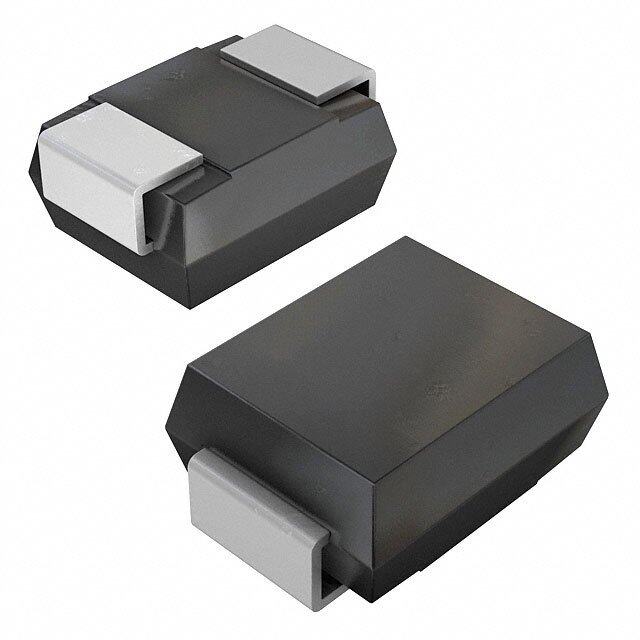
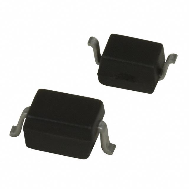
| 产品图片 |
|
| rohs | 符合RoHS无铅 / 符合限制有害物质指令(RoHS)规范要求 |
| 产品系列 | 二极管与整流器,TVS二极管,TVS二极管阵列,ON Semiconductor LC03-6R2G- |
| 数据手册 | |
| 产品型号 | LC03-6R2G |
| 不同频率时的电容 | 16pF @ 1MHz |
| 产品种类 | TVS二极管阵列 |
| 供应商器件封装 | 8-SOIC N |
| 其它名称 | LC03-6R2GOSCT |
| 击穿电压 | 6.8 V |
| 功率-峰值脉冲 | 2000W (2kW) |
| 包装 | 剪切带 (CT) |
| 单向通道 | - |
| 双向通道 | 2 |
| 商标 | ON Semiconductor |
| 安装类型 | 表面贴装 |
| 安装风格 | SMD/SMT |
| 封装 | Reel |
| 封装/外壳 | 8-SOIC(0.154",3.90mm 宽) |
| 封装/箱体 | SOIC-8 |
| 尺寸 | 4 (Max) mm W x 5 (Max) mm L x 1.75 (Max) mm H |
| 峰值浪涌电流 | 100 A |
| 峰值脉冲功率耗散 | 2000 W |
| 工作温度 | -55°C ~ 150°C (TJ) |
| 工作电压 | 5 V |
| 工厂包装数量 | 2500 |
| 应用 | 通用 |
| 最大工作温度 | + 150 C |
| 最小工作温度 | - 55 C |
| 极性 | Unidirectional |
| 标准包装 | 1 |
| 电压-击穿(最小值) | 6.8V |
| 电压-反向关态(典型值) | 5V |
| 电压-箝位(最大值)@Ipp | 20V |
| 电容 | 16 pF |
| 电流-峰值脉冲(10/1000µs) | 100A (8/20µs) |
| 电源线路保护 | 无 |
| 端接类型 | SMD/SMT |
| 类型 | 转向装置(轨至轨) |
| 系列 | LC03-6R2 |
| 通道 | 4 Channels |
| 钳位电压 | 20 V |


- 商务部:美国ITC正式对集成电路等产品启动337调查
- 曝三星4nm工艺存在良率问题 高通将骁龙8 Gen1或转产台积电
- 太阳诱电将投资9.5亿元在常州建新厂生产MLCC 预计2023年完工
- 英特尔发布欧洲新工厂建设计划 深化IDM 2.0 战略
- 台积电先进制程称霸业界 有大客户加持明年业绩稳了
- 达到5530亿美元!SIA预计今年全球半导体销售额将创下新高
- 英特尔拟将自动驾驶子公司Mobileye上市 估值或超500亿美元
- 三星加码芯片和SET,合并消费电子和移动部门,撤换高东真等 CEO
- 三星电子宣布重大人事变动 还合并消费电子和移动部门
- 海关总署:前11个月进口集成电路产品价值2.52万亿元 增长14.8%


PDF Datasheet 数据手册内容提取
LC03-6R2 ESD Protection Diode Low Capacitance Surface Mount ESD Protection for High-Speed Data Interfaces The LC03−6 surge protection is designed to protect equipment www.onsemi.com attached to high speed communication lines from ESD, EFT, and lighting. SO−8 LOW CAPACITANCE Features VOLTAGE SUPPRESSOR • 2 kW PEAK POWER SO−8 Package • Peak Power − 2000 Watts 8 x 20 (cid:2)S 6 VOLTS • ITU K.20 I = 40 A (5/310 (cid:2)s) PP • Bellcore 1089 (Intra−Building) 100 A (2/10 (cid:2)s) PIN CONFIGURATION • ESD Rating: AND SCHEMATIC IEC 61000−4−2 (ESD) 15 kV (air) 8 kV (contact) 1 8 IEC 61000−4−4 (EFT) 40 A (5/50 ns) IEC 61000−4−5 (lighting) 95 A (8/20 (cid:2)s) 2 7 • 3 6 UL Flammability Rating of 94 V−0 • 4 5 Pb−Free Package is Available Typical Applications • High Speed Communication Line Protection SOIC−8 8 CASE 751 1 PLASTIC MAXIMUM RATINGS Rating Symbol Value Unit Peak Power Dissipation Ppk 2000 W MARKING DIAGRAM 8 x 20 (cid:2)S @ TA = 25°C (Note 1) Peak Pulse Current (8 x 20 (cid:2)S Waveform) IPP 100 A 8 Junction and Storage Temperature Range TJ, Tstg −55 to +150 °C ALYCW03W6(cid:2) Lead Solder Temperature − TL 260 °C (cid:2) Maximum 10 Seconds Duration 1 Stresses exceeding those listed in the Maximum Ratings table may damage the device. If any of these limits are exceeded, device functionality should not be assumed, damage may occur and reliability may be affected. LC036 = Device Code 1. Non−repetitive current pulse 8 x 20 (cid:2)S exponential decay waveform A = Assembly Location Y = Year WW = Work Week (cid:2) = Pb−Free Package (Note: Microdot may be in either location) ORDERING INFORMATION Device Package Shipping† LC03−6R2 SO−8 2500/Tape & Reel LC03−6R2G SO−8 2500/Tape & Reel (Pb−Free) †For information on tape and reel specifications, including part orientation and tape sizes, please refer to our Tape and Reel Packaging Specification Brochure, BRD8011/D. © Semiconductor Components Industries, LLC, 2007 1 Publication Order Number: October, 2017 − Rev. 5 LC03−6R2/D
LC03−6R2 ELECTRICAL CHARACTERISTICS Characteristic Symbol Min Typ Max Unit Reverse Breakdown Voltage @ It = 1.0 mA VBR 6.8 − − V Reverse Leakage Current @ VRWN = 5.0 V IR N/A − 20 (cid:2)A Maximum Clamping Voltage @ IPP = 50 A, 8 x 20 (cid:2)S VC N/A − 15 V Maximum Clamping Voltage @ IPP = 100 A, 8 x 20 (cid:2)S VC N/A − 20 V Between I/O Pins and Ground @ VR = 0 V, 1.0 MHz Capacitance − 16 25 pF Between I/O Pins @ VR = 0 Volts, 1.0 MHz Capacitance − 8.0 12 pF TYPICAL CHARACTERISTICS 10 16 14 V) A) GE ( 8 (cid:2)E (12 A G OLT 6 AKA10 V E SE E L 8 ER 4 RS 6 V E E V V, RZ 2 , RER 4 I 2 0 0 −80 −60 −40 −20 0 20 40 60 80 100 120 140 −80 −60 −40 −20 0 20 40 60 80 100 120 140 T, TEMPERATURE (°C) T, TEMPERATURE (°C) Figure 1. Reverse Voltage versus Temperature Figure 2. Reverse Leakage versus Temperature 100 20 tr PEAK VALUE IRSM @ 8 (cid:2)s T 90 18 REN 80 PAUS LTSHEA TW PIDOTIHN T(t PW) HISE DREEF TINHEED E (V) 16 UR 70 PEAK CURRENT DECAY = 8 (cid:2)s AG 14 8 x 20 (cid:2)s Waveform C T E 60 OL 12 ULS 50 HALF VALUE IRSM/2 @ 20 (cid:2)s G V 10 P N K 40 PI 8 A M F PE 30 tP CLA 6 % O 20 V, C 4 10 2 0 0 0 20 40 60 80 0 10 20 30 40 50 60 70 80 90 100 110 t, TIME ((cid:2)s) IPP, PEAK PULSE CURRENT (A) Figure 3. 8 x 20 (cid:2)s Pulse Waveform Figure 4. Clamping Voltage versus Peak Pulse Current www.onsemi.com 2
LC03−6R2 APPLICATIONS INFORMATION The LC03−6 ON Semiconductor’s device is a surge If differential protection is required by some particular protection Diode array designed to protect sensitive applications, then the configuration for differential protection electronics such as communications systems, computers, and is made as shown in the Figure 6: computer peripherals against damage due to transient overvoltage conditions caused by lightning, electrostatic LC03−6 discharge (ESD), and electrical fast transients (EFT). Line 1 Line 1 Because of its relative low capacitance (<25 pf), it can be used In Out N/C N/C in high speed I/O data lines such as USB 1.1 ports. N/C N/C The integrated design of the LC03−6 device offers high Line 2 Line 2 surge rating, low capacitance steering diodes, and a surge In Out protection diode integrated in a single package (SO−8). In addition, this device offers compliance to Bellcore 1089 Figure 6. Configuration for Differential requirements (intra−building). Protection (Line−to−Line) LC03−6 Device’s Configurations Options T1/E1 Linecard Protection (Intra−Building) The Figure 7 shows a typical schematic for a T1/E1 line Protection of Two High−speed I/O Data Lines card protection circuit. The LC03−6 device is connected The LC03−6 device is able to protect two high speed data between Tip and Ring on the transmit and receive line pairs. lines against transient overvoltage conditions by driving it provides protection to metallic and common mode lightning them to a fixed reference point for clamping purposes. surges per Bellcore 1089 intra−building (For further Depending in the application’s requirements, the LC03−6 information, see Bellcore 1089 standard). A metallic voltage device can be configured for protection in either differential is defined as a difference of potential between the T and R mode (Line−to−Line) or common mode (Line−to−ground). terminals of a telecommunications pair. Currents caused by The Figure 5 shows the connection for Differential mode lightning, in the absence of protector operation and with (Line−to−Line) and Common mode (Line−to−Ground) balanced terminal equipment and telecommunications loop, protection. The inputs and outputs of the I/O data lines are cause Tip and Ring conductors to attain the same potential connected at terminals 1 to 8, and 4 to 5 while the terminals hence do not produce metallic transients. Common mode 2, 3, 6 and 7 are connected to ground; for better performance, surges are suppressed by the isolation of the transformer. it is recommended to minimize parasitic inductances by using ground planes and minimizing the PCB trace lengths for the ground return connections. LC03−6 Line 1 Line 1 In Out Line 2 Line 2 In Out Figure 5. Configuration for Differential and Common Mode Protection www.onsemi.com 3
LC03−6R2 PTC R1 RTIP R3 LC03−6 R2 RRING T1 PTC T1/E1 TRANSCEIVER R4 PTC TTIP LC03−6 R5 TRING T2 PTC Figure 7. Typical T1 Line Card Protection ESD Protection in USB 1.1 Port Applications transient condition which reduces significantly the As we know, a USB port is composed of four lines. The performance of the ESD protection circuit. The LC03−6 lines D+ and D− are used for bi−directional data device provides a unique surge protection Diode array transmission, and the remaining two lines are reserved for designed to protect two I/O data lines (single USB port) bus voltage and ground. Since USB is a hot plugging and against damage due to ESD conditions or transient voltage unplugging system, all its four lines have the risk to receive conditions. Because of its low capacitance, it can be used in ESD conditions in the real field of the application. high speed I/O data lines such as USB 1.1 components. In Typical ESD protection techniques are commonly formed addition to its low capacitance characteristics, the LC03−6 by the combination of different discrete semiconductor device from ONSemiconductor complies with the most products which make this technique obsolete and common industrial standards for ESD, EFT and surge non−efficient because the interconnections of the discrete protection: IEC61000−4−2, IEC61000−4−4, devices increase the parasitic inductance effects during a IEC61000−4−5. www.onsemi.com 4
LC03−6R2 PACKAGE DIMENSIONS SOIC−8 NB CASE 751−07 ISSUE AK NOTES: −X− 1. DIMENSIONING AND TOLERANCING PER ANSI Y14.5M, 1982. A 2. CONTROLLING DIMENSION: MILLIMETER. 3. DIMENSION A AND B DO NOT INCLUDE MOLD PROTRUSION. 4. MAXIMUM MOLD PROTRUSION 0.15 (0.006) 8 5 PER SIDE. 5. DIMENSION D DOES NOT INCLUDE DAMBAR B S 0.25 (0.010) M Y M PROTRUSION. ALLOWABLE DAMBAR PROTRUSION SHALL BE 0.127 (0.005) TOTAL 1 IN EXCESS OF THE D DIMENSION AT −Y− 4 K 6. 7M5A1X−I0M1U TMH RMUA T7E51R−IA0L6 CAROEN DOIBTSIOONL.ETE. NEW STANDARD IS 751−07. G MILLIMETERS INCHES DIM MIN MAX MIN MAX A 4.80 5.00 0.189 0.197 C NX 45(cid:3) B 3.80 4.00 0.150 0.157 SEATING C 1.35 1.75 0.053 0.069 PLANE D 0.33 0.51 0.013 0.020 −Z− G 1.27 BSC 0.050 BSC H 0.10 0.25 0.004 0.010 0.10 (0.004) J 0.19 0.25 0.007 0.010 H D M J K 0.40 1.27 0.016 0.050 M 0 (cid:3) 8 (cid:3) 0 (cid:3) 8 (cid:3) N 0.25 0.50 0.010 0.020 0.25 (0.010)M Z Y S X S S 5.80 6.20 0.228 0.244 SOLDERING FOOTPRINT* 1.52 0.060 7.0 4.0 0.275 0.155 0.6 1.270 0.024 0.050 (cid:2) (cid:3) mm SCALE 6:1 inches *For additional information on our Pb−Free strategy and soldering details, please download the ON Semiconductor Soldering and Mounting Techniques Reference Manual, SOLDERRM/D. www.onsemi.com 5
LC03−6R2 ON Semiconductor and are trademarks of Semiconductor Components Industries, LLC dba ON Semiconductor or its subsidiaries in the United States and/or other countries. ON Semiconductor owns the rights to a number of patents, trademarks, copyrights, trade secrets, and other intellectual property. A listing of ON Semiconductor’s product/patent coverage may be accessed at www.onsemi.com/site/pdf/Patent−Marking.pdf. ON Semiconductor reserves the right to make changes without further notice to any products herein. ON Semiconductor makes no warranty, representation or guarantee regarding the suitability of its products for any particular purpose, nor does ON Semiconductor assume any liability arising out of the application or use of any product or circuit, and specifically disclaims any and all liability, including without limitation special, consequential or incidental damages. Buyer is responsible for its products and applications using ON Semiconductor products, including compliance with all laws, regulations and safety requirements or standards, regardless of any support or applications information provided by ON Semiconductor. “Typical” parameters which may be provided in ON Semiconductor data sheets and/or specifications can and do vary in different applications and actual performance may vary over time. All operating parameters, including “Typicals” must be validated for each customer application by customer’s technical experts. ON Semiconductor does not convey any license under its patent rights nor the rights of others. ON Semiconductor products are not designed, intended, or authorized for use as a critical component in life support systems or any FDA Class 3 medical devices or medical devices with a same or similar classification in a foreign jurisdiction or any devices intended for implantation in the human body. Should Buyer purchase or use ON Semiconductor products for any such unintended or unauthorized application, Buyer shall indemnify and hold ON Semiconductor and its officers, employees, subsidiaries, affiliates, and distributors harmless against all claims, costs, damages, and expenses, and reasonable attorney fees arising out of, directly or indirectly, any claim of personal injury or death associated with such unintended or unauthorized use, even if such claim alleges that ON Semiconductor was negligent regarding the design or manufacture of the part. ON Semiconductor is an Equal Opportunity/Affirmative Action Employer. This literature is subject to all applicable copyright laws and is not for resale in any manner. PUBLICATION ORDERING INFORMATION LITERATURE FULFILLMENT: N. American Technical Support: 800−282−9855 Toll Free ON Semiconductor Website: www.onsemi.com Literature Distribution Center for ON Semiconductor USA/Canada 19521 E. 32nd Pkwy, Aurora, Colorado 80011 USA Europe, Middle East and Africa Technical Support: Order Literature: http://www.onsemi.com/orderlit Phone: 303−675−2175 or 800−344−3860 Toll Free USA/Canada Phone: 421 33 790 2910 Fax: 303−675−2176 or 800−344−3867 Toll Free USA/Canada Japan Customer Focus Center For additional information, please contact your local Email: orderlit@onsemi.com Phone: 81−3−5817−1050 Sales Representative ◊ www.onsemi.com LC03−6R2/D 6
Mouser Electronics Authorized Distributor Click to View Pricing, Inventory, Delivery & Lifecycle Information: O N Semiconductor: LC03-6R2G