ICGOO在线商城 > 集成电路(IC) > 接口 - 驱动器,接收器,收发器 > LAN8820I-ABZJ
 Datasheet下载
- 型号: LAN8820I-ABZJ
- 制造商: Microchip
- 库位|库存: xxxx|xxxx
- 要求:
| 数量阶梯 | 香港交货 | 国内含税 |
| +xxxx | $xxxx | ¥xxxx |
查看当月历史价格
查看今年历史价格
LAN8820I-ABZJ产品简介:
ICGOO电子元器件商城为您提供LAN8820I-ABZJ由Microchip设计生产,在icgoo商城现货销售,并且可以通过原厂、代理商等渠道进行代购。 LAN8820I-ABZJ价格参考。MicrochipLAN8820I-ABZJ封装/规格:接口 - 驱动器,接收器,收发器, 全 收发器 1/1 以太网 56-QFN(8x8)。您可以下载LAN8820I-ABZJ参考资料、Datasheet数据手册功能说明书,资料中有LAN8820I-ABZJ 详细功能的应用电路图电压和使用方法及教程。
LAN8820I-ABZJ 是由 Microchip Technology 提供的一款接口芯片,属于驱动器、接收器和收发器类别。该型号主要应用于以太网通信领域,支持 10/100Mbps 的快速以太网连接。以下是其主要应用场景:

1. 工业自动化
   LAN8820I-ABZJ 可用于工业控制设备中,例如 PLC(可编程逻辑控制器)、HMI(人机界面)以及数据采集系统。它通过提供稳定可靠的以太网连接,实现设备之间的高效通信。

2. 嵌入式系统
   在需要网络功能的嵌入式设备中,这款芯片可以作为以太网物理层(PHY)解决方案,为微控制器或处理器提供网络接入能力。例如智能家居设备、物联网节点等。

3. 消费类电子产品
   它适用于各种需要联网功能的家用设备,如打印机、路由器、IP 摄像头以及多媒体播放器。这些设备可以通过 LAN8820I-ABZJ 实现与局域网或其他设备的互联互通。

4. 汽车电子
   在车载信息娱乐系统和远程诊断模块中,这款芯片可用于构建车内网络,支持车辆与外部网络的数据交换。

5. 医疗设备
   医疗仪器如监护仪、超声波设备等可能需要实时传输大量数据到中央服务器或云端。LAN8820I-ABZJ 能够满足此类设备对高可靠性和低延迟的要求。

6. 网络基础设施
   该芯片也可用于小型网络交换机、网桥或接入点的设计,帮助扩展家庭或办公室网络覆盖范围。

总之,LAN8820I-ABZJ 凭借其高性能、低功耗和易于集成的特点,在需要快速以太网连接的各种场景中具有广泛的应用价值。
| 参数 | 数值 |
| 产品目录 | 集成电路 (IC)半导体 |
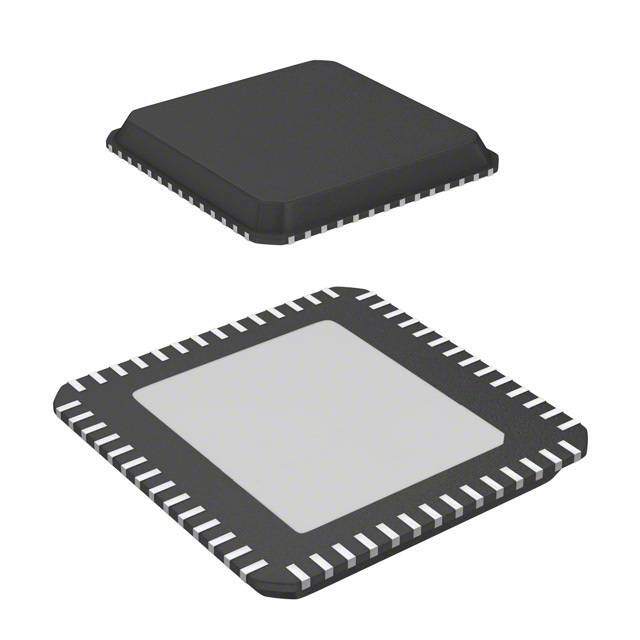
| 描述 | TXRX ETHERNET 54VQFN以太网 IC |
| 产品分类 | |
| 品牌 | Microchip Technology |
| 产品手册 | |
| 产品图片 | |
| rohs | 符合RoHS无铅 / 符合限制有害物质指令(RoHS)规范要求 |
| 产品系列 | 通信及网络 IC,以太网 IC,Microchip Technology LAN8820I-ABZJ* |
| 数据手册 | |
| 产品型号 | LAN8820I-ABZJ |
| PCN组件/产地 | http://www.microchip.com/mymicrochip/NotificationDetails.aspx?id=5836&print=view |
| 产品 | Ethernet Transceivers |
| 产品种类 | 以太网 IC |
| 以太网连接类型 | 10 Base-T, 100 Base-TX, 1000 Base-T |
| 商标 | Microchip Technology |
| 安装风格 | SMD/SMT |
| 封装 | Tray |
| 封装/箱体 | QFN-56 |
| 工厂包装数量 | 260 |
| 支持协议 | CSMA/CD |
| 支持标准 | 802.3, 802.3AB, 802.3u |
| 收发器数量 | 1 Transceiver |
| 数据速率 | 10 Mb/s, 100 Mb/s, 1000 Mb/s |
| 最大功率耗散 | 1081 mW |
| 最大工作温度 | + 85 C |
| 最大电源电流 | 460 mA |
| 最小工作温度 | - 40 C |
| 标准包装 | 260 |
| 电源电压-最大 | 3.6 V |
| 电源电压-最小 | 1.14 V |
| 类型 | 10/100/1000 Ethernet Transceiver |


- 商务部:美国ITC正式对集成电路等产品启动337调查
- 曝三星4nm工艺存在良率问题 高通将骁龙8 Gen1或转产台积电
- 太阳诱电将投资9.5亿元在常州建新厂生产MLCC 预计2023年完工
- 英特尔发布欧洲新工厂建设计划 深化IDM 2.0 战略
- 台积电先进制程称霸业界 有大客户加持明年业绩稳了
- 达到5530亿美元!SIA预计今年全球半导体销售额将创下新高
- 英特尔拟将自动驾驶子公司Mobileye上市 估值或超500亿美元
- 三星加码芯片和SET,合并消费电子和移动部门,撤换高东真等 CEO
- 三星电子宣布重大人事变动 还合并消费电子和移动部门
- 海关总署:前11个月进口集成电路产品价值2.52万亿元 增长14.8%


PDF Datasheet 数据手册内容提取
LAN8820/LAN8820i RGMII 10/100/1000 Ethernet Transceiver with HP Auto-MDIX Support Highlights Key Benefits • Single-Chip Ethernet Physical Layer Transceiver • High-Performance 10/100/1000 Ethernet Trans- (PHY) ceiver • Compliant with IEEE 802.3ab (1000BASE-T), - Compliant with IEEE 802.3ab (1000BASE-T) IEEE 802.3u (Fast Ethernet), and ISO 802-3/IEEE - Compliant with IEEE 802.3/802.3u (Fast 802.3 (10BASE-T) Ethernet) • HP Auto-MDIX support in accordance with IEEE - Compliant with ISO 802-3/IEEE 802.3 802.3ab specification at 10/100/1000 Mbps oper- (10BASE-T) ation - 10BASE-T, 100BASE-TX and 1000BASE-T • Miniature 56-pin QFN lead-free RoHS compliant support package with RGMII (8 x 8 x 0.85mm height) - Loop-back modes • Implements Reduced Power Operating Modes - Auto-negotiation (NEXT page support) - Automatic polarity detection and correction - Link status change wake-up detection Target Applications - Vendor specific register functions • Set-Top Boxes - Supports reduced pin count RGMII interface • Networked Printers and Servers - Controlled impedance outputs - Supports RGMII ID mode • Test Instrumentation - Three status LED outputs • LAN on Motherboard - Compliant with IEEE 802.3-2005 standards • Embedded Telecom Applications - RGMII pins tolerant to 3.6V • Video Record/Playback Systems - Integrated DSP implements adaptive equal- • Cable Modems/Routers izer, echo cancelers, and crosstalk cancelers • DSL Modems/Routers - Efficient digital baseline wander correction • Digital Video Recorders • Power and I/Os • IP and Video Phones - Various low power modes • Wireless Access Points - 2.5V I/O supply • Digital Televisions • Miscellaneous Features • Digital Media Adapters/Servers - IEEE 1149.1 (JTAG) boundary scan • Gaming Consoles - Multiple clock options - 25MHz crystal or • POE Applications 25MHz single-ended clock • Packaging - 56-pin QFN (8x8 mm) RoHS compliant pack- age with RGMII • Environmental - Commercial temperature range (0°C to +70°C) - Industrial temperature range (-40°C to +85°C) 2009-2018 Microchip Technology Inc. DS00001871D-page 1
LAN8820/LAN8820i TO OUR VALUED CUSTOMERS It is our intention to provide our valued customers with the best documentation possible to ensure successful use of your Microchip products. To this end, we will continue to improve our publications to better suit your needs. Our publications will be refined and enhanced as new volumes and updates are introduced. If you have any questions or comments regarding this publication, please contact the Marketing Communications Department via E-mail at docerrors@microchip.com. We welcome your feedback. Most Current Data Sheet To obtain the most up-to-date version of this data sheet, please register at our Worldwide Web site at: http://www.microchip.com You can determine the version of a data sheet by examining its literature number found on the bottom outside corner of any page. The last character of the literature number is the version number, (e.g., DS30000000A is version A of document DS30000000). Errata An errata sheet, describing minor operational differences from the data sheet and recommended workarounds, may exist for cur- rent devices. As device/documentation issues become known to us, we will publish an errata sheet. The errata will specify the revision of silicon and revision of document to which it applies. To determine if an errata sheet exists for a particular device, please check with one of the following: • Microchip’s Worldwide Web site; http://www.microchip.com • Your local Microchip sales office (see last page) When contacting a sales office, please specify which device, revision of silicon and data sheet (include -literature number) you are using. Customer Notification System Register on our web site at www.microchip.com to receive the most current information on all of our products. DS00001871D-page 2 2009-2018 Microchip Technology Inc.
LAN8820/LAN8820i Table of Contents 1.0 Introduction .....................................................................................................................................................................................4 2.0 Pin Description and Configuration ..................................................................................................................................................5 3.0 Functional Description ..................................................................................................................................................................13 4.0 Register Descriptions ....................................................................................................................................................................34 5.0 Operational Characteristics ...........................................................................................................................................................60 6.0 Package Outline ............................................................................................................................................................................76 Appendix A: Data Sheet Revision History ...........................................................................................................................................78 The Microchip Web Site ......................................................................................................................................................................81 Customer Change Notification Service ...............................................................................................................................................81 Customer Support ...............................................................................................................................................................................81 Product Identification System .............................................................................................................................................................82 2009-2018 Microchip Technology Inc. DS00001871D-page 3
LAN8820/LAN8820i 1.0 INTRODUCTION The LAN8820/LAN8820i is a low-power 10BASE-T/100BASE-TX/1000BASE-T Gigabit Ethernet physical layer (PHY) transceiver that is fully compliant with the IEEE 802.3 and 802.3ab standards. The LAN8820/LAN8820i can be configured to communicate with an Ethernet MAC via the standard RGMII interface. It contains a full-duplex transceiver for 1000Mbps operation on four pairs of category 5 or better balanced twisted pair cable. Per IEEE 802.3-2005 standards, all digital interface pins are tolerant to 3.6V. The LAN8820/LAN8820i is configurable via hardware and software, supporting both IEEE 802.3-2005 compliant and vendor-specific register functions via SMI. The LAN8820/LAN8820i implements Auto-Negotiation to automatically determine the best possible speed and duplex mode of operation. HP Auto-MDIX support allows the use of direct con- nect or crossover cables. An internal block diagram of the LAN8820/LAN8820i is shown in Figure1-1. A typical system-level diagram is shown in Figure1-2. FIGURE 1-1: INTERNAL BLOCK DIAGRAM 3 3 3 3 3 PLL Digital TX 2 2 2 2 2 1 1 Scrambler 1 0 1 0 1 Trellis LEDs 4DPAM-5 Encoders Spectral Analog LEDs 0 Shaper 0 TX 0 3 2 RGMII Physical 1 10/100/1000 SCuobdlainyge r 0 Ethernet Active Hybrid JTAG TAP 3 3 3 3 3 2 1 0 Controller Digital RX 2 2 2 2 1 1 Descrambler 1 0 1 0 Viterbi Decoder 4DPAM-5 Decoders Analog DSP 0 0 RX LAN8820/LAN8820i FIGURE 1-2: SYSTEM LEVEL BLOCK DIAGRAM Crystal 10/100/1000 RGMII LAN8820/ MDI Ethernet Ethernet Ethernet MAC LAN8820i Magnetics JTAG SLtaEtDus DS00001871D-page 4 2009-2018 Microchip Technology Inc.
LAN8820/LAN8820i 2.0 PIN DESCRIPTION AND CONFIGURATION FIGURE 2-1: 56-QFN PIN ASSIGNMENTS (TOP VIEW) TR0N 43 28 TXCTRL TR0P 44 27 TXD0 VDD12A 45 26 TXD1 LAN8820/LAN8820i TR1N 46 56 PIN QFN 25 TXD2 TR1P 47 (TOP VIEW) 24 VDD25IO VDD12A 48 23 VDD12CORE VDD12BIAS 49 22 TXD3 VSS VDD12PLL 50 21 NC TR2N 51 20 VDD12CORE TR2P 52 19 VDD25IO VDD12A 53 18 RXC TR3N 54 17 IRQ TR3P 55 16 nRESET VDD12A 56 15 HPD NOTE: Exposed pad (VSS) on bottom of package must be connected to ground 2009-2018 Microchip Technology Inc. DS00001871D-page 5
LAN8820/LAN8820i TABLE 2-1: RGMII INTERFACE PINS Num Buffer Name Symbols Description Pins Type Transmit Data 0 TXD0 IS The MAC transmits data to the PHY using this 1 (PD) signal. Transmit Data 1 TXD1 IS The MAC transmits data to the PHY using this 1 (PD) signal. Transmit Data 2 TXD2 IS The MAC transmits data to the PHY using this 1 (PD) signal. Transmit Data 3 TXD3 IS The MAC transmits data to the PHY using this 1 (PD) signal. Transmit TXCTRL IS Indicates both the transmit data enable (TXEN) and 1 Control (PD) transmit error (TXER) functions per the RGMII specification. Transmit Clock TXC IS Used to latch data from the MAC into the PHY. (PD) 1 1000BASE-T: 125MHz 100BASE-TX: 25MHz 10BASE-T: 2.5MHz Receive Data 0 RXD0 O6 The PHY transfers data to the MAC using this 1 signal. Receive Data 1 RXD1 O6 The PHY transfers data to the MAC using this 1 signal. Receive Data 2 RXD2 O6 The PHY transfers data to the MAC using this 1 signal. Receive Data 3 RXD3 O6 The PHY transfers data to the MAC using this 1 signal. Receive Control RXCTRL O6 Indicates both the receive data valid (RXDV) and 1 receive error (RXER) functions per the RGMII specification. Receive Clock RXC O6 Used to transfer data to the MAC. 1 1000BASE-T: 125MHz 100BASE-TX: 25MHz 10BASE-T: 2.5MHz Note 2-1 Configuration strap values are latched on hardware reset. Configuration straps are identified by an underlined symbol name. Signals that function as configuration straps must be augmented with an external resistor when connected to a load. Refer to Section 3.8, "Configuration," on page23 for additional information. DS00001871D-page 6 2009-2018 Microchip Technology Inc.
LAN8820/LAN8820i TABLE 2-2: SERIAL MANAGEMENT INTERFACE (SMI) PINS Num Buffer Name Symbols Description Pins Type SMI Clock MDC IS Serial Management Interface clock. 1 (PD) SMI Data Input/ MDIO IS/O8 Serial Management Interface data input/output. 1 Output (PU) TABLE 2-3: LED & CONFIGURATION PINS Num Buffer Name Symbols Description Pins Type 10BASE-T Link 10_LED O8 10BASE-T LED link indication. Refer to Section 1 LED Indicator 3.9.1, "LEDs," on page27 for additional information. 100BASE-TX 100_LED O8 100BASE-TX LED link indication. Refer to Section Link LED 3.9.1, "LEDs," on page27 for additional Indicator information. Hardware HPD_MODE IS This configuration strap is used to select the Power Down (PD) Hardware Power Down (HPD) mode. When pulled- (HPD) Mode up, the PLL is not disabled when HPD is asserted. 1 Configuration When pulled-down, the PLL is disabled when HPD is asserted. Strap Refer to Section 3.7.3, "Hardware Power-Down," on page23 for additional information. See Note 2-2 for more information on configuration straps. 1000BASE-T 1000_LED O8 1000BASE-T LED link indication. Refer to Section Link LED 3.9.1, "LEDs," on page27 for additional Indicator information. RGMII ID Mode RGMII_ID_MODE IS This configuration strap is used to configure the Enable (PD) RGMII PHY TXC/RXC delay enable bit defaults. 1 Configuration When pulled-up, the RGMII PHY TXC/RXC delays Strap are enabled by default. When pulled-down, the RGMII PHY TXC/RXC delays are disabled be default. Refer to Section 3.3, "RGMII Interface," on page18 for more information. See Note 2-2 for more information on configuration straps. Configuration CONFIG0 IS This pin sets the PHYADD[1:0] bits of the 10/100 Input 0 (PD) Special Modes Register on reset or power-up. It must be connected to VSS, 100_LED, 1000_LED, 1 or VDD25IO. Refer to Section 3.8.1.2, "CONFIG[3:0] Configuration Pins," on page24 for additional information. Configuration CONFIG1 IS This pin sets the PAUSE bit of the Auto Negotiation Input 1 (PD) Advertisement Register and PHYADD [2] bit of the 10/100 Special Modes Register on reset or power- 1 up. It must be connected to VSS, 100_LED, 1000_LED, or VDD25IO. Refer to Section 3.8.1.2, "CONFIG[3:0] Configuration Pins," on page24 for additional information. 2009-2018 Microchip Technology Inc. DS00001871D-page 7
LAN8820/LAN8820i TABLE 2-3: LED & CONFIGURATION PINS (CONTINUED) Num Buffer Name Symbols Description Pins Type Configuration CONFIG2 IS This pin sets the MOD[1:0] bits of the Extended Input 2 (PD) Mode Control/Status Register on reset or power- up. It must be connected to VSS, 100_LED, 1 1000_LED, or VDD25IO. Refer to Section 3.8.1.2, "CONFIG[3:0] Configuration Pins," on page24 for additional information. Configuration CONFIG3 IS This pin sets the MOD[3] bit of the Extended Mode Input 3 (PD) Control/Status Register on reset or power-up. It 1 must be connected to 1000_LED. Refer to Section 3.8.1.2, "CONFIG[3:0] Configuration Pins," on page24 for additional information. Note 2-2 Configuration strap values are latched on hardware reset. Configuration straps are identified by an underlined symbol name. Signals that function as configuration straps must be augmented with an external resistor when connected to a load. Refer to Section 3.8, "Configuration," on page23 for additional information. TABLE 2-4: ETHERNET PINS Buffer Num Pins Name Symbol Description Type Ethernet TX/ TR0P AIO Transmit/Receive Positive Channel 0. 1 RX Positive Channel 0 Ethernet TX/ TR0N AIO Transmit/Receive Negative Channel 0. 1 RX Negative Channel 0 Ethernet TX/ TR1P AIO Transmit/Receive Positive Channel 1. 1 RX Positive Channel 1 Ethernet TX/ TR1N AIO Transmit/Receive Negative Channel 1. 1 RX Negative Channel 1 Ethernet TX/ TR2P AIO Transmit/Receive Positive Channel 2. 1 RX Positive Channel 2 Ethernet TX/ TR2N AIO Transmit/Receive Negative Channel 2. 1 RX Negative Channel 2 Ethernet TX/ TR3P AIO Transmit/Receive Positive Channel 3. 1 RX Positive Channel 3 Ethernet TX/ TR3N AIO Transmit/Receive Negative Channel 3. 1 RX Negative Channel 3 External PHY ETHRBIAS AI Used for the internal bias circuits. Connect to an 1 Bias Resistor external 8.06K 1.0% resistor to ground. DS00001871D-page 8 2009-2018 Microchip Technology Inc.
LAN8820/LAN8820i TABLE 2-5: JTAG PINS Buffer Num Pins Name Symbol Description Type JTAG Test TDO O8 JTAG (IEEE 1149.1) data output. 1 Data Out JTAG Test TDI IS JTAG (IEEE 1149.1) data input. 1 Data Input (PU) Note: When not used, tie this pin to VDD25IO. JTAG Test TCK IS JTAG (IEEE 1149.1) test clock. 1 Clock (PD) Note: When not used, tie this pin to VSS. JTAG Test TMS IS JTAG (IEEE 1149.1) test mode select. 1 Mode Select (PU) Note: When not used, tie this pin to VDD25IO. TABLE 2-6: MISCELLANEOUS PINS Buffer Num Pins Name Symbol Description Type Crystal Input XI ICLK External 25MHz crystal input. Note: This pin can also be driven by a 25MHz single-ended clock oscillator. When this 1 method is used, XO should be left unconnected. Refer to Section 5.6, "Clock Circuit," on page75 for additional information. Crystal XO OCLK External 25MHz crystal output. 1 Output System Reset nRESET IS This active-low pin allows external hardware to 1 (PU) reset the device. 1 Interrupt IRQ O6 Programmable interrupt request. Request Note: When used, this pin requires an external 4.7K pull-up resistor. Hardware HPD IS When asserted, this pin places the device into Power Down (PD) Hardware Power Down (HPD) mode. Refer to 1 Section 3.7.3, "Hardware Power-Down," on page23 for additional information. No Connect NC - This pin must be left floating for normal device 1 operation. 2009-2018 Microchip Technology Inc. DS00001871D-page 9
LAN8820/LAN8820i TABLE 2-7: POWER PINS Buffer Num Pins Name Symbol Description Type +2.5V VDD25IO P +2.5V I/O power. I/O Power Refer to Section 3.10, "Application Diagrams," on 4 Supply Input page31 and the LAN8820/LAN8820i reference schematics for connection information. Digital Core VDD12CORE P Refer to Section 3.10, "Application Diagrams," on 6 +1.2V Power page31 and the LAN8820/LAN8820i reference Supply Input schematics for connection information. Ethernet VDD12A P Refer to Section 3.10, "Application Diagrams," on +1.2V Port page31 and the LAN8820/LAN8820i reference 4 Power Supply schematics for connection information. Input For Channels 0-3 1 Ethernet VDD12BIAS P Refer to Section 3.10, "Application Diagrams," on +1.2V Bias page31 and the LAN8820/LAN8820i reference Power Supply schematics for connection information. Input Ethernet PLL VDD12PLL P Refer to Section 3.10, "Application Diagrams," on 1 +1.2V Power page31 and the LAN8820/LAN8820i reference Supply Input schematics for connection information. Note 2-3 Ground VSS P Common Ground Note 2-3 Exposed pad on package bottom (Figure2-1). DS00001871D-page 10 2009-2018 Microchip Technology Inc.
LAN8820/LAN8820i TABLE 2-8: 56-QFN PIN ASSIGNMENTS Pin Pin Pin Pin Pin Name Pin Name Pin Name Pin Name Num Num Num Num 1 TDI 15 HPD 29 TXC 43 TR0N 2 TCK 16 nRESET 30 VDD12CORE 44 TR0P 3 TMS 17 IRQ 31 1000_LED/ 45 VDD12A RGMII_ID_MODE 4 TDO 18 RXC 32 100_LED/ 46 TR1N HPD_MODE 5 XI 19 VDD25IO 33 10_LED 47 TR1P 6 XO 20 VDD12CORE 34 CONFIG3 48 VDD12A 7 VDD25IO 21 NC 35 CONFIG2 49 VDD12BIAS 8 VDD12CORE 22 TXD3 36 VDD12CORE 50 VDD12PLL 9 RXD0 23 VDD12CORE 37 VDD25IO 51 TR2N 10 RXD1 24 VDD25IO 38 CONFIG1 52 TR2P 11 RXD2 25 TXD2 39 CONFIG0 53 VDD12A 12 RXD3 26 TXD1 40 MDC 54 TR3N 13 VDD12CORE 27 TXD0 41 MDIO 55 TR3P 14 RXCTRL 28 TXCTRL 42 ETHRBIAS 56 VDD12A EXPOSED PAD MUST BE CONNECTED TO VSS 2009-2018 Microchip Technology Inc. DS00001871D-page 11
LAN8820/LAN8820i 2.1 Buffer Types TABLE 2-9: BUFFER TYPES Buffer Type Description IS Schmitt-triggered input. O6 Output with 6mA sink and 6mA source. O8 Output with 8mA sink and 8mA source. PU 50uA (typical) internal pull-up. Unless otherwise noted in the pin description, internal pull- ups are always enabled. Note: Internal pull-up resistors prevent unconnected inputs from floating. Do not rely on internal resistors to drive signals external to the device. When connected to a load that must be pulled high, an external resistor must be added. PD 50uA (typical) internal pull-down. Unless otherwise noted in the pin description, internal pull-downs are always enabled. Note: Internal pull-down resistors prevent unconnected inputs from floating. Do not rely on internal resistors to drive signals external to the device. When connected to a load that must be pulled low, an external resistor must be added. AI Analog input. AIO Analog bi-directional. ICLK Crystal oscillator input pin. OCLK Crystal oscillator output pin. P Power pin. Note1: The digital signals are not 5V tolerant. Refer to Section 5.1, "Absolute Maximum Ratings*," on page60 for additional buffer information. DS00001871D-page 12 2009-2018 Microchip Technology Inc.
LAN8820/LAN8820i 3.0 FUNCTIONAL DESCRIPTION This chapter provides functional descriptions of the various device features. These features have been categorized into the following sections: • Auto-negotiation • HP Auto-MDIX • RGMII Interface • Serial Management Interface (SMI) • Interrupt Management • Resets • Power-Down modes • Configuration • Miscellaneous Functions • Application Diagrams 3.1 Auto-negotiation The purpose of the auto-negotiation function is to automatically configure the PHY to the optimum link parameters based on the capabilities of its link partner. Auto-negotiation is a mechanism for exchanging configuration information between two link-partners and automatically selecting the highest performance mode of operation supported by both sides. Auto- negotiation is fully defined in clause 28 and clause 40 of the IEEE 802.3 specification. Once auto-negotiation has completed, information about the resolved link can be passed back to the controller via the integrated Serial Management Interface (SMI). The results of the negotiation process are reflected in the Speed Indica- tion field of the PHY Special Control / Status Register as well as the Auto Negotiation Link Partner Ability Register. The advertised capabilities of the PHY are stored in Auto Negotiation Advertisement Register. The defaults advertised by the device are determined as described in Section 3.8.1.2.2, "Configuring the Mode of Operation (CONFIG[3:2])," on page26. The auto-negotiation protocol is a purely physical layer activity and proceeds independently of the MAC controller. When enabled, auto-negotiation is started by the occurrence of one of the following events: • Hardware reset • Software reset • Power-down reset • Link status down • Setting the Restart Auto-Negotiate bit of the Basic Control Register On detection of one of these events, the device begins auto-negotiation by transmitting bursts of Fast Link Pulses (FLP). The data transmitted by an FLP burst is known as a “Link Code Word.” This exchange of information allows link partners to determine the Highest Common Ability (HCD). Once a capability match has been determined, the link code words are repeated with the acknowledge bit set. Any dif- ference in the main content of the link code words at this time will cause auto-negotiation to re-start. Auto-negotiation will also re-start if all of the required FLP bursts are not received. Writing the 100BASE-TX Full Duplex, 100BASE-TX, 10BASE-T Full Duplex, and 10BASE-T bits of the Auto Negotiation Advertisement Register allows software control of the advertised capabilities. However, writing the Auto Negotiation Advertisement Register does not automatically re-start auto-negotiation. The Restart Auto-Negotiate bit of the Basic Control Register must be set before the new abilities will be advertised. Auto-negotiation can also be disabled via soft- ware by clearing the Auto-Negotiation Enable bit of the Basic Control Register. Auto-Negotiation also resolves the Master/Slave clocking relationship between two PHYs for a 1000BASE-T link. Refer to Section 3.1.4, "Master/Slave," on page14 for additional information. 3.1.1 RESTARTING AUTO-NEGOTIATION Auto-negotiation can be restarted at any time by using the Restart Auto-Negotiate bit of the Basic Control Register. Auto-negotiation will also re-start if the link is broken at any time. A broken link is caused by signal loss. This may occur because of a cable break, or because of an interruption in the signal transmitted by the Link Partner. Auto-negotiation resumes in an attempt to determine the new link configuration. 2009-2018 Microchip Technology Inc. DS00001871D-page 13
LAN8820/LAN8820i If the management entity restarts Auto-negotiation by writing to the Restart Auto-Negotiate bit, the device will respond by stopping all transmission/receiving operations. Auto-negotiation will restart after approximately 1200mS. The Link Partner will have also dropped the link and will resume auto-negotiation. 3.1.2 DISABLING AUTO-NEGOTIATION Auto-negotiation can be disabled via software by clearing the Auto-Negotiation Enable bit of the Basic Control Register. The device will then force its speed of operation to reflect the information in the Speed Select[1], Speed Select[0], and Duplex Mode bits of the Basic Control Register. These bits are ignored when auto-negotiation is enabled. 3.1.3 PARALLEL DETECTION If the LAN8820/LAN8820i is connected to a device lacking the ability to auto-negotiate (for example, no FLPs are detected), it is able to determine the speed of the link based on either 100M MLT-3 symbols or 10M Normal Link Pulses. In this case, the link is presumed to be half-duplex per the IEEE standard. This ability is known as “Parallel Detection”. This feature ensures inter operability with legacy link partners. The Ethernet MAC has access to information regarding parallel detect via the Auto Negotiation Expansion Register. If a link is formed via parallel detection, the Link Partner Auto-Negotiation Able bit of the Auto Negotiation Expansion Reg- ister is cleared to indicate that the Link Partner is not capable of auto-negotiation. If a fault occurs during parallel detec- tion, the Parallel Detection Fault bit of this register is set. The Auto Negotiation Link Partner Ability Register is updated with information from the link partner which is coded in the received FLPs. If the Link Partner is not auto-negotiation capable, then the Auto Negotiation Link Partner Ability Register is updated after completion of parallel detection to reflect the speed capability of the Link Partner. Parallel detect cannot be used to establish Gigabit Ethernet links because echo cancellation and signal recovery on a Gigabit Ethernet link requires resolution of the Master/Slave clock relationship, which requires the exchange of FLPs. 3.1.4 MASTER/SLAVE In 1000BASE-T, one of the two link partner devices must be configured as Master and the other as Slave. The Master device transmits data using the local clock, while the Slave device uses the clock recovered from incoming data. The Master and Slave assignments are set using the configuration pins as described in Section 3.8.1.2.2, "Configuring the Mode of Operation (CONFIG[3:2])," on page26 or by using the Master/Slave Manual Config Enable and Master/ Slave Manual Config Value bits of the Master/Slave Control Register. If both the link partner and the local device are manually given the same Master/Slave assignment, an error will be indicated in the Master/Slave Configuration Fault bit of the Master/Slave Status Register. Depending on the link partner configuration, the manual Master/Slave mode can be resolved to sixteen possible out- comes, as shown in Table3-1. TABLE 3-1: MASTER/SLAVE RESOLUTION FOR 1000BASE-T LAN8820/LAN8820i Link Partner Advertisement Advertisement LAN8820/LAN8820i Result Link Partner Result Single-Port Single-Port M/S resolved by random seed M/S resolved by random seed Single-Port Multi-Port Slave Master Single-Port Manual Master Slave Master Single-Port Manual Slave Master Slave Multi-Port Single-Port Master Slave Multi-Port Multi-Port M/S resolved by random seed M/S resolved by random seed Multi-Port Manual Master Slave Master Multi-Port Manual Slave Master Slave Manual Master Single-Port Master Slave DS00001871D-page 14 2009-2018 Microchip Technology Inc.
LAN8820/LAN8820i TABLE 3-1: MASTER/SLAVE RESOLUTION FOR 1000BASE-T (CONTINUED) LAN8820/LAN8820i Link Partner Advertisement Advertisement LAN8820/LAN8820i Result Link Partner Result Manual Master Multi-Port Master Slave Manual Master Manual Master No Link No Link Manual Master Manual Slave Master Slave Manual Slave Single-Port Slave Master Manual Slave Multi-Port Slave Master Manual Slave Manual Master Slave Master Manual Slave Manual Slave No Link No Link 3.1.5 MANUAL OPERATION The device supports a manual (forced) operation for test purposes. In manual operation, the user sets the link speed (10Mbps or 100Mbps) and the duplex state (full or half). Auto-negotiation must be disabled in order to manually configure the speed and the duplex. This may be accomplished using the configuration pins, as described in Section 3.8.1.2.2, "Configuring the Mode of Operation (CONFIG[3:2])," on page26, or by using the Basic Control Register as described in Section 3.1.2, "Disabling Auto-negotiation," on page14. For 10BASE-T and 100BASE-TX, the link state of the device is determined by the Speed Select[1], Speed Select[0], and Duplex Mode bits of the Basic Control Register. Manual operation at a link speed of 1000Mbps is not supported. 3.1.6 HALF VS. FULL-DUPLEX Half-duplex operation relies on the CSMA/CD (Carrier Sense Multiple Access / Collision Detect) protocol to handle net- work traffic and collisions. In this mode, the internal carrier sense signal, CRS, responds to both transmit and receive activity. If data is received while the PHY is transmitting, a collision results. In full-duplex mode, the PHY is able to transmit and receive data simultaneously and collision detection is disabled. In this mode, the internal CRS responds only to receive activity. In 10BASE-T and 100BASE-T mode, CRS is redefined to respond only to received activity. In 1000BASE-T, CRS is disabled. Table3-2 describes the behavior of the internal CRS bit under all receive/transmit conditions. TABLE 3-2: CRS BEHAVIOR CRS Behavior Mode Speed Duplex Activity (Note 3-1) Manual 10 Mbps Half-Duplex Transmitting Active Manual 10 Mbps Half-Duplex Receiving Active Manual 10 Mbps Full-Duplex Transmitting Low Manual 10 Mbps Full-Duplex Receiving Active Manual 100 Mbps Half-Duplex Transmitting Active Manual 100 Mbps Half-Duplex Receiving Active Manual 100 Mbps Full-Duplex Transmitting Low Manual 100 Mbps Full-Duplex Receiving Active Auto-Negotiation 10 Mbps Half-Duplex Transmitting Active 2009-2018 Microchip Technology Inc. DS00001871D-page 15
LAN8820/LAN8820i TABLE 3-2: CRS BEHAVIOR (CONTINUED) CRS Behavior Mode Speed Duplex Activity (Note 3-1) Auto-Negotiation 10 Mbps Half-Duplex Receiving Active Auto-Negotiation 10 Mbps Full-Duplex Transmitting Low Auto-Negotiation 10 Mbps Full-Duplex Receiving Active Auto-Negotiation 100 Mbps Half-Duplex Transmitting Active Auto-Negotiation 100 Mbps Half-Duplex Receiving Active Auto-Negotiation 100 Mbps Full-Duplex Transmitting Low Auto-Negotiation 100 Mbps Full-Duplex Receiving Active Note 3-1 The internal CRS signal operates in two modes: Active and Low. When in Active mode, the internal CRS will transition high and low upon line activity, where a high value indicates a carrier has been detected. In Low mode, the internal CRS stays low and does not indicate carrier detection. 3.2 HP Auto-MDIX HP Auto-MDIX facilitates the use of CAT-5 (100BASE-T) media UTP interconnect cable without consideration of inter- face wiring scheme. If a user plugs in either a direct connect LAN cable, or a crossover patch cable, as shown in Figure3-1, the Auto-MDIX PHY is capable of configuring the twisted pair pins for correct transceiver operation. The internal logic of the device detects the TX and RX pins of the connecting device. It can automatically re-assign chan- nel 0 and 1 if required to establish a link. In 1000BASE-T mode, it can re-assign channel 2 and 3. Crossover resolution precedes the actual auto-negotiation process that involves exchange of FLPs to advertise capabilities. Automatic MDI/ MDIX is described in IEEE 802.3ab Clause 40, section 40.8.2. Since the RX and TX line pairs are interchangeable, spe- cial PCB design considerations are needed to accommodate the symmetrical magnetics and termination of an Auto- MDIX design. Auto-MDIX is enabled by default, and can be disabled by the Auto MDIX Disable bit in the 10/100 Mode Control/Status Register. When Auto-MDIX is disabled, the TX and RX pins can be configured manually by the MDI/MDI-X 0:1 and MDI/ MDI-X 2:3 bits in the Extended Mode Control/Status Register. The device includes an advanced crossover resolution capability called Semi Crossover. This is an extension to HP Auto-MDIX that corrects for a cable with only two pairs crossed. If Semi Crossover is enabled, after the device has attempted to establish a link with all four signal pairs normal or crossed, it will attempt to establish a link with pairs 2/3 switched and 0/1 straight, and then with pairs 0/1 switched and pairs 2/3 straight. The Semi Crossover is enabled by default, and can be disabled by the Semi Crossover Enable bit in the 10/100 Mode Control/Status Register. After resolution of crossed pairs is complete, using either HP Auto-MDIX or the Semi Crossover function, the MDI/MDI- X status is reported through the XOVER Resolution 0:1 and XOVER Resolution 2:3 bits of the User Status 2 Register. DS00001871D-page 16 2009-2018 Microchip Technology Inc.
LAN8820/LAN8820i FIGURE 3-1: CABLE CONNECTION TYPES: STRAIGHT-THROUGH, CROSSOVER, SEMI CROSSOVER RJ-45 8-pin Straight-Through RJ-45 8-pin Crossover TR0P 1 1 TR0P TR0P 1 1 TR0P TR0N 2 2 TR0N TR0N 2 2 TR0N TR1P 3 3 TR1P TR1P 3 3 TR1P TR2P 4 4 TR2P TR2P 4 4 TR2P TR2N 5 5 TR2N TR2N 5 5 TR2N TR1N 6 6 TR1N TR1N 6 6 TR1N TR3P 7 7 TR3P TR3P 7 7 TR3P TR3N 8 8 TR3N TR3N 8 8 TR3N Direct Connect Cable Crossover Cable RJ-45 8-pin Semi Crossover RJ-45 8-pin Semi Crossover TR0P 1 1 TR0P TR0P 1 1 TR0P TR0N 2 2 TR0N TR0N 2 2 TR0N TR1P 3 3 TR1P TR1P 3 3 TR1P TR2P 4 4 TR2P TR2P 4 4 TR2P TR2N 5 5 TR2N TR2N 5 5 TR2N TR1N 6 6 TR1N TR1N 6 6 TR1N TR3P 7 7 TR3P TR3P 7 7 TR3P TR3N 8 8 TR3N TR3N 8 8 TR3N 0/1 Straight, 2/3 Crossed 0/1 Crossed, 2/3 Straight 3.2.1 REQUIRED ETHERNET MAGNETICS The magnetics selected for use with the device should be an Auto-MDIX style magnetic available from several vendors. Refer to Application Note 8.13 “Suggested Magnetics” for the latest qualified and suggested magnetics. Vendors and part numbers are provided in this application note. 2009-2018 Microchip Technology Inc. DS00001871D-page 17
LAN8820/LAN8820i 3.3 RGMII Interface The device communicates with an external MAC using the Reduced Gigabit Media Independent Interface (RGMII). The RGMII is compliant with the RGMII standard, and provides support for 1000BASE-T, 100BASE-TX, or 10BASE-T oper- ation. The RGMII consists of the RXC, RXD[3:0], RXCTRL, TXC, TXD[3:0] and TXCTRL signals. All transmission related sig- nals, TXC, TXD[3:0] and TXCTRL, are generated by the MAC. The TXC transmit clock is used to synchronize the TXD[3:0] data and TXCTRL control signals. All reception related signals, RXC, RXD[3:0] and RXCTRL, are generated by the device. The RXC receive clock is used to synchronic the RXD[3:0] data and RXCTRL control signals. The RGMII interface supports both Version 1.3 and Version 2.0 of the RGMII specification. Version 1.3 of the RGMII Specification requires a 1.5 to 2ns clock delay via a PCB trace delay. Version 2.0 of the RGMII Specification introduces the option of an on-chip Internal Delay (ID). These distinct RGMII modes of operation are referred to as “Non-ID Mode” and “ID Mode”, respectively, throughout the document. Refer to the RGMII specification for additional details. In addition to the standard Non-ID and ID modes of operation, the device supports a hybrid mode of operation, for a total of 3 RGMII modes. These modes are summarized below: Non-ID Mode - Per the RGMII specification, no internal delay is generated at the MAC or the device(PHY). External PCB trace delays are required to meet RGMII timing requirements. ID Mode - Per the RGMII specification, an internal delay is generated on TXC at the MAC, and an ID is generated on RXC at the device(PHY). No PCB trace delay is required. Hybrid Mode - In this mode, the device(PHY) will generate an ID on both TXC and RXC. This mode may be used to eliminate the PCB trace delay requirement when utilizing a non-ID MAC. The RGMII mode is configured via the RGMII PHY TXC Delay Enable and RGMII PHY RXC Delay Enable bits of the Control / Status Indications Register (29.[9:8]). The default values of these bits are configured via the RGMII_ID_MODE configuration strap. Figure3-2 details the RGMII mode configuration logic. For additional information on the RGMII_ID_- MODE configuration strap, refer to Section 3.8.1.1, "Configuration Straps," on page24. FIGURE 3-2: RGMII MODE CONFIGURATION LOGIC LAN8820/LAN8820i RGMII_ID_MODE RGMII PHY TXC Delay Enable Bit TXC Delay (From MAC) PHY TX Logic TXD[3:0] (From MAC) RGMII PHY RXC Delay Enable Bit RXC Delay (To MAC) PHY RX Logic RXD[3:0] (To MAC) DS00001871D-page 18 2009-2018 Microchip Technology Inc.
LAN8820/LAN8820i The various RGMII modes and their corresponding configuration settings are summarized in Figure3-3. FIGURE 3-3: RGMII MODES OF OPERATION Non-ID Mode (RGMII Specification) (27.[9:8] = 00b, RGMII_ID_MODE = 0) TXC TXC PCB Trace Delay TXD[3:0] TXD[3:0] LAN8820/ MAC LAN8820i RXD[3:0] RXD[3:0] RXC RXC PCB Trace Delay RGMII PHY TXC Delay: Disabled RGMII PHY RXC Delay: Disabled ID Mode (RGMII Specification) (27.[9:8] = 01b) TXC TXC ID TXD[3:0] TXD[3:0] LAN8820/ MAC LAN8820i RXD[3:0] RXD[3:0] RXC RXC ID RGMII PHY TXC Delay: Disabled RGMII PHY RXC Delay: Enabled Hybrid Mode (27.[9:8] = 11b, RGMII_ID_MODE = 1) TXC TXC ID TXD[3:0] TXD[3:0] LAN8820/ MAC RXD[3:0] RXD[3:0] LAN8820i RXC RXC ID RGMII PHY TXC Delay: Enabled RGMII PHY RXC Delay: Enabled Note: Strapping RGMII_ID_MODE high sets the device into Hybrid Mode. In order to set the device into ID Mode, the RGMII PHY TXC Delay Enable and RGMII PHY RXC Delay Enable bits of the Control / Status Indica- tions Register (27.[9:8]) must be configured via software to 01b. Timing information for the RGMII interface is provided in Section 5.5, "AC Specifications," on page65. For additional information on the RGMII interface, refer to the RGMII specification. 2009-2018 Microchip Technology Inc. DS00001871D-page 19
LAN8820/LAN8820i 3.3.1 MII ISOLATE MODE The device may be configured to electrically isolate the RGMII pins by setting the Isolate bit of the Basic Control Reg- ister. In this mode, all MAC data interface output pins are HIGH and all MAC data interface input pins are ignored. In this mode, the SMI interface is kept active, allowing the MAC to access the SMI registers and generate interrupts. All MDI operations are halted while in isolate mode. 3.4 Serial Management Interface (SMI) The Serial Management Interface is used to control the device and obtain its status. This interface supports the standard PHY registers required by Clause 22 of the 802.3 standard, as well as “vendor-specific” registers allowed by the spec- ification. Non-supported registers (such as 11 to 14) will be read as hexadecimal “FFFF”. Device registers are detailed in Section 4.0, "Register Descriptions," on page34. At the system level, SMI provides 2 signals: MDIO and MDC. The MDC signal is an aperiodic clock provided by the station management controller (SMC). MDIO is a bi-directional data SMI input/output signal that receives serial data (commands) from the controller SMC and sends serial data (status) to the SMC. The minimum time between edges of the MDC is 160 ns. There is no maximum time between edges. The minimum cycle time (time between two consecutive rising or two consecutive falling edges) is 400 ns. These modest timing requirements allow this interface to be easily driven by the I/O port of a microcontroller. The data on the MDIO line is latched on the rising edge of the MDC. The frame structure and timing of the data is shown in Figure1-1 and Figure1-2. The timing relationships of the MDIO signals are further described in Section 5.5.6, "SMI Timing," on page73. FIGURE 3-4: MDIO TIMING AND FRAME STRUCTURE - READ CYCLE Read Cycle MDC ... MDIO 32 1's 0 1 1 0 A4 A3 A2 A1 A0 R4 R3 R2 R1 R0 D15 D14 ... D1 D0 Start of OP Turn Preamble PHY Address Register Address Data Frame Code Around Data To Phy Data From Phy FIGURE 3-5: MDIO TIMING AND FRAME STRUCTURE - WRITE CYCLE Write Cycle MDC ... MDIO 32 1's 0 1 0 1 A4 A3 A2 A1 A0 R4 R3 R2 R1 R0 D15 D14 ... D1 D0 Start of OP Turn Preamble PHY Address Register Address Data Frame Code Around Data To Phy DS00001871D-page 20 2009-2018 Microchip Technology Inc.
LAN8820/LAN8820i 3.5 Interrupt Management The device supports multiple interrupt capabilities which are not a part of the IEEE 802.3 specification. An active low asynchronous interrupt signal may be generated on the IRQ pin when selected events are detected, as configured by the Interrupt Mask Register. To set an interrupt, the corresponding mask bit in the Interrupt Mask Register must be set (see Table3-3). When the associated event occurs, the IRQ pin will be asserted. When the corresponding event to deassert IRQ is true, the IRQ pin will be deasserted. All interrupts are masked following a reset. Note: Table3-3 utilizes register index and bit number referencing in lieu of individual names. For example, “30.10” is used to reference bit 10 (transmitter elastic buffer overflow interrupt enable) of the Interrupt Mask Register (register index 30). TABLE 3-3: INTERRUPT MANAGEMENT TABLE Event to Assert Event to Deassert Mask Interrupt Source Flag Interrupt Source IRQ IRQ 30.15:11 29.15:11 RESERVED -NA- -NA- -NA- -NA- 30.10 29.10 Transmitter Elastic -NA- -NA- Transmitter Elastic Overflow condition Buffer Overflow (Note 3-3) Buffer Overflow resolved 30.9 29.9 Transmitter Elastic -NA- -NA- Transmitter Elastic Underflow condition Buffer Underflow (Note 3-3) Buffer Underflow resolved 30.8 29.8 Idle Error Count 10.7:0 Idle Error Count Idle Error Count Reading register 10 Overflow Overflow 30.7 29.7 ENERGYON 17.1 ENERGYON Rising 17.1 Falling 17.1 or (Note 3-2) Reading register 29 30.6 29.6 Auto-Negotiation 1.5 Auto-Negotiate Rising 1.5 Falling 1.5 or complete Complete Reading register 29 30.5 29.5 Remote Fault 1.4 Remote Fault Rising 1.4 Falling 1.4, or Detected Reading register 1 or Reading register 29 30.4 29.4 Link Down 1.2 Link Status Falling 1.2 Reading register 1 or Reading register 29 30.3 29.3 RESERVED -NA- -NA- -NA- -NA- 30.2 29.2 Parallel Detection 6.4 Parallel Rising 6.4 Falling 6.4 or Fault Detection Fault Reading register 6, or Reading register 29 or Re-AutoNegotiate or Link down 30.1 29.1 Auto-Negotiation 6.1 Page Received Rising 6.1 Falling of 6.1 or Page Received Reading register 6, or Reading register 29 Re-auto-negotiate, or Link Down. Note 3-2 The ENERGYON bit of the 10/100 Mode Control/Status Register (17.1) defaults to “1” after a hardware reset. If no energy is detected before 256mS, the ENERGYON bit will be cleared. When ENERGYON is “0” and energy is detected, due to the establishment of a valid link or the PHY auto- negotiation moving past the ability detect state, the ENERGYON bit will be set and the INT7 bit of the Interrupt Source Flags Register will assert. If ENERGYON is set and the energy is removed, the INT7 bit will assert. The ENERGYON bit will clear 256mS after the interrupt. If the PHY is in manual mode, INT7 will be asserted 256mS after the link is broken. If the PHY is auto-negotiating, INT7 will be asserted 256mS after the PHY returns to the ability detect state (maximum of 1.5S after the link 2009-2018 Microchip Technology Inc. DS00001871D-page 21
LAN8820/LAN8820i is broken). To prevent an unexpected assertion of IRQ, the ENERGYON interrupt mask (INT7_EN) should always be cleared as part of the ENERGYON interrupt service routine. Note 3-3 The transmitter FIFO depth can be adjusted via the Transmitter FIFO Depth field of the Extended Mode Control/Status Register (19.10:9). 3.6 Resets The device provides the following chip-level reset sources: • Hardware Reset (nRESET) • Software Reset • Power-Down Reset 3.6.1 HARDWARE RESET (NRESET) Note: System implementers should connect the nRESET input pin to an output pin from the respective MAC or microcontroller, so that the required power-up sequence can be performed without causing a full system reset event. A hardware reset will occur when the system reset nRESET input pin is driven low. Anytime nRESET is asserted, it must be held low for the minimum time specified in Section 5.5.4, "Reset Timing," on page68 to ensure proper reset to the PHY. Following a hardware reset, the device resets the device registers and relatches the configuration straps and CON- FIG[3:0] pins. On first power-up of the device, the sequence below must be also be followed to ensure the device exits reset in the correct operational state: 1. Perform a hardware reset on power-up as per Section 5.5.3, "Power-On Hardware Reset Timing," on page67. 2. Wait a minimum of 250mS 3. Write SMI Register 0 (Basic Control Register) = 0x4040 4. Wait a minimum of 1 second 5. Assert the nRESET input pin (nRESET = 0) 6. Wait a minimum of 50mS 7. Deassert the nRESET input pin (nRESET = 1) After completing this sequence, the LAN8820/LAN8820i will be in the default states and ready for any initialization or configuration and allow operation. Note: A hardware reset (nRESET assertion) is required following power-up. Refer to Section 5.5.3, "Power-On Hardware Reset Timing," on page67 for additional information. 3.6.2 SOFTWARE RESET A software reset is initiated by writing a ‘1’ to the PHY Soft Reset (RESET) bit of the Basic Control Register. This self- clearing bit will return to ‘0’ after approximately 256s, at which time the PHY reset is complete. This reset initializes the logic within the PHY, with the exception of register bits marked as “NASR” (Not Affected by Software Reset). Following a software reset, the device configuration is reloaded from the register bit values, and not from the configura- tion straps and CONFIG[3:0] pins. The device does not relatch the hardware configuration settings. For example, if the device is powered up and a configuration strap is changed from its initial power up state, a software reset will not load the new strap setting. DS00001871D-page 22 2009-2018 Microchip Technology Inc.
LAN8820/LAN8820i 3.6.3 POWER-DOWN RESET A power-down reset is automatically activated when the device comes out of the power-down mode. During power- down, the registers are not reset. Configuration straps and CONFIG[3:0] pins are not latched as a result of a power- down reset. The power-down reset is internally extended by 256 s after exiting the power-down mode to allow the PLLs to stabilize before the logic is released from reset. Refer to Section 3.7, "Power-Down modes," on page23 for details on the various power-down modes. 3.7 Power-Down modes The device supports 3 power-down modes: • General Power-Down • Energy Detect Power-Down • Hardware Power-Down 3.7.1 GENERAL POWER-DOWN This power-down mode is controlled by the Power Down bit of the Basic Control Register. In this mode, the entire device is powered-down except for the serial management interface. The device remains in the general power-down mode while Power Down is set. When Power Down is cleared, the device powers up and is automatically reset (via a Power- Down Reset). For maximum power savings, auto-negotiation should be disabled before enabling the general power- down mode. 3.7.2 ENERGY DETECT POWER-DOWN This power-down mode is controlled by the EDPWRDOWN bit of the 10/100 Mode Control/Status Register. In this mode, when no energy is present on the line, nothing is transmitted and the device is powered-down except for the manage- ment interface, the SQUELCH circuit and the ENERGYON logic. The ENERGYON bit in the 10/100 Mode Control/Status Register is asserted when there is valid energy from the line (100BASE-TX, 10BASE-T, or Auto-Negotiation signals) and the PHY powers-up. It automatically resets itself into the previous state prior to power-down, and stays in active mode as long as energy exists on the line. If the ENGERGYON interrupt is enabled (INT7_EN of the Interrupt Mask Register), IRQ is asserted. Note: The first and possibly second packet to activate ENERGYON may be lost. 3.7.3 HARDWARE POWER-DOWN This power-down mode is controlled by the HPD pin. In this mode, the entire device is powered-down except for the serial management interface. The HPD_MODE configuration strap selects whether the PLL will be shut down when in hardware power-down mode. To exit the hardware power-down mode, the HPD pin must be deasserted, followed by the deassertion of the Power Down bit in the Basic Control Register. If the hardware power-down mode is set to shut down the PLL, a software reset must also be issued. Note1: The device will wake-up in the hardware power-down mode if the HPD pin is asserted during hardware reset. 2: For additional information on the HPD_MODE configuration strap, refer to Section 3.8.1.1, "Configuration Straps," on page24. 3.8 Configuration The device mode of operation may be controlled by hardware and software (register-selectable) configuration options. The initial configuration may be selected in hardware as described in Section3.8.1. In addition, register-selectable soft- ware configuration options may be used to further define the functionality of the transceiver as described in Section3.8.2. The device supports both IEEE 802.3-2005 compliant and vendor-specific register functions. 3.8.1 HARDWARE CONFIGURATION Hardware configuration is controlled via multiple configuration straps and the CONFIG[3:0] configuration pins. These items are detailed in the following sub-sections. 2009-2018 Microchip Technology Inc. DS00001871D-page 23
LAN8820/LAN8820i 3.8.1.1 Configuration Straps Configuration straps are multi-function pins that are driven as outputs during normal operation. During a Hardware Reset (nRESET), these outputs are tri-stated. The high or low state of the signal is latched following de-assertion of the reset and is used to determine the default configuration of a particular feature. Table3-4 details the configuration straps. Configuration straps are also listed as part of Section 2.0, "Pin Description and Configuration," on page5 with underlined names. Configuration straps include internal resistors in order to prevent the signal from floating when unconnected. If a partic- ular configuration strap is connected to a load, an external pull-up or pull-down should be used to augment the internal resistor to ensure that it reaches the required voltage level prior to latching. The internal resistor can also be overridden by the addition of an external resistor. Note1: The system designer must guarantee that configuration straps meet the timing requirements specified in Section 5.5.3, "Power-On Hardware Reset Timing," on page67. If configuration straps are not at the correct voltage level prior to being latched, the device may capture incorrect strap values. 2: Configuration straps must never be driven as inputs. If required, configuration straps can be augmented, or overridden with external resistors. TABLE 3-4: CONFIGURATION STRAPS Configuration Logic 0 Logic 1 Description Strap (PD) (PU) HPD_MODE Selects the hardware power-down (HPD) mode HPD with PLL HPD with PLL disabled (Default) enabled RGMII_ID_MODE Configures the RGMII PHY TXC/RXC delay 27.[9:8] = 00b 27.[9:8] = 11b enable bits of the Control / Status Indications (Default) Register (27.[9:8]). Refer to Section 3.3, "RGMII Interface," on page18 for additional information. 3.8.1.2 CONFIG[3:0] Configuration Pins The device provides 4 dedicated configuration pins, CONFIG[3:0], which are used to select the default SMI address and mode of operation. The CONFIG[3:0] configuration pins differ from configuration straps in that they are single-purpose pins and have different latch timing requirements. The high or low states of the CONFIG[3:0] pins are latched following deassertion of a Hardware Reset (nRESET). Refer to Section 5.5.3, "Power-On Hardware Reset Timing," on page67 for additional CONFIG[3:0] timing information. Each CONFIG[3:0] configuration pin can be connected in one of four ways. The Configuration Pin Value (CPV) repre- sented by each connection option is shown in Table3-5. TABLE 3-5: HARDWARE CONNECTION DETERMINES CONFIGURATION PIN VALUE (CPV) CONFIG[X] Value Connects to: GND CPV(0) 100_LED CPV(1) 1000_LED CPV(2) VDD CPV(3) Using the CPV nomenclature for each CONFIG[3:0] pin, Section3.8.1.2.1 describes how to configure the SMI address and Section3.8.1.2.2 describes how to configure the initial mode of operation. DS00001871D-page 24 2009-2018 Microchip Technology Inc.
LAN8820/LAN8820i Note: The HPD pin is also a dedicated configuration pin. HPD forces the entire device to power down except for the management interface. The Hardware Power-Down mode is described in Section 3.7.3, "Hardware Power-Down," on page23. 3.8.1.2.1 Configuring the SMI Address (CONFIG[1:0]) The SMI address may be configured via hardware to any value between 0 and 7. If an address greater than 7 is required, the user can configure the PHY address using Software Configuration via the PHYADD[4:0] field of the 10/100 Special Modes Register (after SMI communication at an address is established). The CONFIG1 pin is used to configure both the SMI address and the value of the Pause Operation (PAUSE) bit in the Auto Negotiation Advertisement Register. The user must first determine the desired PAUSE value. The configuration pin values for CONFIG1 and CONFIG0 should then be selected using Table3-6 (PAUSE=0) or Table3-7 (PAUSE=1), respectively. TABLE 3-6: SMI ADDRESS CONFIGURATION WITH PAUSE=0 PHYADD[2:0] CONFIG1 CONFIG0 000 CPV(0) CPV(0) 001 CPV(0) CPV(1) 010 CPV(0) CPV(2) 011 CPV(0) CPV(3) 100 CPV(1) CPV(0) 101 CPV(1) CPV(1) 110 CPV(1) CPV(2) 111 CPV(1) CPV(3) TABLE 3-7: SMI ADDRESS CONFIGURATION WITH PAUSE=1 PHYADD[2:0] CONFIG1 CONFIG0 000 CPV(2) CPV(0) 001 CPV(2) CPV(1) 010 CPV(2) CPV(2) 011 CPV(2) CPV(3) 100 CPV(3) CPV(0) 101 CPV(3) CPV(1) 110 CPV(3) CPV(2) 111 CPV(3) CPV(3) 2009-2018 Microchip Technology Inc. DS00001871D-page 25
LAN8820/LAN8820i 3.8.1.2.2 Configuring the Mode of Operation (CONFIG[3:2]) This section describes the initial modes of operation that are available using the CONFIG[3:2] configuration pins. The user may configure additional modes using Software Configuration when the CONFIG[3:2] options do not include the desired mode. The CONFIG3 pin is used to configure the values of the MOD field (19.15:11) The configuration pin values for CONFIG3 and CONFIG2 should be selected using Table3-8. These tables also detail how the MOD field of the Extended Mode Control/Status Register will be configured. Section3.8.1.2.3 describes how the MOD field controls other configuration bits in the device. When a soft reset is issued via the PHY Soft Reset (RESET) bit of the Basic Control Register, configuration is controlled by the register bit values and the CONFIG[3:0] pins have no affect. Likewise, changing the MOD field of the Extended Mode Control/Status Reg- ister bits does not change the configuration of the device in this case. Note: Table3-8 utilizes register index and bit number referencing in lieu of individual names. TABLE 3-8: CONFIGURING THE MODE OF OPERATION Reg 19 Mode Definitions CONFIG3 CONFIG2 [15:11] All mode capable (10/100/1000). Auto-negotiation enabled. CPV(2) CPV(0) 10111 Auto master/slave resolution single port. All mode capable (10/100/1000). Auto-negotiation enabled. CPV(2) CPV(1) 11000 Auto master/slave resolution multi-port. All mode capable (10/100/1000). Auto-negotiation enabled. CPV(2) CPV(2) 11001 Manual master/slave resolution slave port. All mode capable (10/100/1000). Auto-negotiation enabled. CPV(2) CPV(3) 11010 Manual master/slave resolution master port. 3.8.1.2.3 Configuration Bits Impacted by the Mode of Operation Immediately after a reset, the MOD field of the Extended Mode Control/Status Register will be set dependent on the configuration pin values of the CONFIG3 and CONFIG2 pins, as described in Section3.8.1.2.2. Table3-9 details how the MOD field effects other device configuration register bits. Note: Table3-9 utilizes register index and bit number referencing in lieu of individual names DS00001871D-page 26 2009-2018 Microchip Technology Inc.
LAN8820/LAN8820i TABLE 3-9: REGISTER BITS IMPACTED BY THE MODE OF OPERATION (MOD) Reg 19 Reg 0 Reg 4 Reg 9 Mode Definitions [15:11] [13,12,8,6] [8,7,6,5] [12,11,10,9,8] 00000 - RESERVED - - - 10110 10111 All capable. Auto-negotiation enabled. 01X1 1111 00011 Auto master/slave resolution single port. 11000 All capable. Auto-negotiation enabled. 01X1 1111 01111 Auto master/slave resolution multi-port. 11001 All capable. Auto-negotiation enabled. 01X1 1111 10011 Manual master/slave resolution slave port. 11010 All capable. Auto-negotiation enabled. 01X1 1111 11111 Manual master/slave resolution master port. 11011 - RESERVED - - - 11111 3.8.2 SOFTWARE CONFIGURATION The Serial Management Interface (SMI) allows for the configuration and control of multiple transceivers. Several 16-bit status and control registers are accessible through the management interface pins MDC and MDIO for 10/100/ 1000Mbps operation. The device implements all the required MII registers and optional registers as described in Sec- tion 4.0, "Register Descriptions". Configuring the SMI address is described in Section3.8.1.2.1. Refer to Section 3.4, "Serial Management Interface (SMI)," on page20 for additional information on the SMI. 3.9 Miscellaneous Functions 3.9.1 LEDS The device provides the following LED signals to enable visual indication of status: • 1000_LED • 100_LED • 10_LED The Speed LEDs (1000_LED, 100_LED, 10_LED) are driven after a link is established. The functional operation of each LED is detailed in TABLE 3-10:. TABLE 3-10: LED OPERATION LED STATUS DESCRIPTION On 1000BASE-T link 1000_LED Blinking Transmit/receive activity On 100BASE-T link 100_LED Blinking Transmit/receive activity On 10BASE-T link 10_LED Blinking Transmit/receive activity 2009-2018 Microchip Technology Inc. DS00001871D-page 27
LAN8820/LAN8820i 3.9.2 ISOLATE MODE The device data paths may be electrically isolated from the RGMII interface by setting the Isolate bit of the Basic Control Register to “1”. In isolation mode, the transceiver does not respond to the TXD and TXCTRL inputs, but does respond to management transactions. Isolation provides a means for multiple transceivers to be connected to the same RGMII interface without contention. By default, the transceiver is not isolated (on power-up, Isolate=0). 3.9.3 CARRIER SENSE The carrier sense signal is output on RXCTRL. Carrier sense operation is defined in the IEEE 802.3u standard. The PHY asserts carrier sense based only on receive activity whenever the PHY is either in repeater mode or full-duplex mode. Otherwise, the PHY asserts carrier sense based on either transmit or receive activity. The carrier sense logic uses the encoded, unscrambled data to determine carrier activity status. It activates carrier sense with the detection of 2 non-contiguous zeros within any 10 bit span. Carrier sense terminates if a span of 10 con- secutive ones is detected before a /J/K/ Start-of Stream Delimiter pair. If an SSD pair is detected, carrier sense is asserted until either /T/R/ End–of-Stream Delimiter pair or a pair of IDLE symbols is detected. Carrier is negated after the /T/ symbol or the first IDLE. If /T/ is not followed by /R/, then carrier is maintained. Carrier is treated similarly for IDLE followed by some non-IDLE symbol. 3.9.4 LINK INTEGRITY This section details the establishment, maintenance and removal of links between the device and a link partner in 1000BASE-T, 100BASE-TX and 10BASE-T modes. Link status is reported in the Link Status bit of the Basic Status Reg- ister. The link status is also used to drive the device LEDs as described in Section 3.9.1, "LEDs," on page27. 3.9.4.1 Establishing and Maintaining a Link Once a link state is determined via auto-negotiation, parallel detection, or forced operation, the device and the link part- ner establish a link. The completion of the auto-negotiation process is reported via the Auto-Negotiate Complete bit of the Basic Status Reg- ister and issues an interrupt as described in Section 3.5, "Interrupt Management," on page21. The speed of the link is reported in the Speed Indication field of the PHY Special Control / Status Register. The speed is also reported on the LED pins for any link. Failure to complete the auto-negotiation process is reported through the following status bits: • Parallel Detection Fault reported in the Auto Negotiation Expansion Register while operating in 10BASE-T or 100BASE-TX modes. • Master/Slave Configuration Fault reported in the Master/Slave Status Register while operating in 1000BASE-T mode. A fault occurs if the Master/Slave configuration conditions do not allow master/slave resolution, as defined in the Master/ Slave Manual Config Enable and Master/Slave Manual Config Value bits in the Master/Slave Control Register of the local and remote link partners. 3.9.4.2 1000BASE-T For 1000BASE-T links, the device and its link partner enter a training phase after completion of the auto-negotiation process. The links exchange idle symbols and use the information obtained from receiving this signal to set their adap- tive filter coefficients. These coefficients are used in the receiver to equalize the incoming signal, as well as eliminate signal impairments such as echo and cross-talk. Each side indicates completion of the training phase to its link partner by changing the encoding of the idle-symbols it transmits. The link is established after both sides indicate completion of the training phase. Each side continues to send idle sym- bols whenever it has no data to transmit. The link is maintained as long as valid idle, data, or carrier extension symbols are received. Status of both local and remote receivers is reported in the Local Receiver Status and Remote Receiver Status bits of the Master/Slave Status Register. DS00001871D-page 28 2009-2018 Microchip Technology Inc.
LAN8820/LAN8820i The device also provides an advanced Auto Link Breaker feature (only for 1000BASE-T links). Using this feature, the link can be taken down if the bit error rate (BER) exceeds the threshold defined in Link Break Threshold field of the Link Control Register. The error counting occurs during the idle time for a period commensurate with the specified BER. The Auto Link Breaker feature is enabled via the Link Break Enable bit of the Link Control Register. 3.9.4.3 100BASE-TX For 100BASE-TX links, the device and its link partner begin transmitting idle symbols after completion of the auto-nego- tiation process. Each side continues sending idle symbols whenever it has no data to transmit. The link is maintained as long as valid idle symbols or data are received. 3.9.4.4 10BASE-T For 10BASE-T links, the device and its link partner begin exchanging normal link pulses (NLPs) after completion of the auto-negotiation process. The device transmits an NLP every 16ms and expects to receive an NLP every 8 to 24ms. A link is maintained as long as NLPs are received. 3.9.4.5 Taking Down a Link The device takes down an established link when the required conditions are no longer met. When a link is down, data transmission stops. For 10BASE-T links, the link is taken down after NLPs are no longer received. For 100BASE-TX and 1000BASE-T links, the link is taken down after valid idle codes are no longer received. After a link is down, the device does the following: • If auto-negotiation is enabled, the device re-enters the auto-negotiation phase and begins transmitting FLPs • If auto-negotiation is not enabled, the device transmits NLPs in 10BASE-T mode, and MLT-3s in 100BASE-TX mode. 3.9.5 SPEED OPTIMIZER The Speed Optimize function is designed to resolve the issue of using auto-negotiation to establish a link on impaired cable plants. Examples of impaired cable plants for 1000BASE-T (Gigabit) connections include: • Channel 2 twisted pair cable plant is broken • Channel 3 twisted pair cable plant is broken • Channel 2 and 3 twisted pair cable plants are broken • Cable plant is too long Examples of impaired cable plants for 100BASE-TX connections include: • Cable plant is too long • Using wrong cable plant (such as CAT-3) The Speed Optimize function requires the MAC to support 1000/100/10Mbps speeds, 1000/100Mbps speeds, 1000/ 10Mbps or 100/10Mbps speeds. If a link fails to establish after the link partners go through auto-negotiation several times at the HCD (Highest Common Denominator), the device advertises the next highest-allowable speed (as set in the Auto Negotiation Advertisement Register) and restarts auto-negotiation with the new speed. When 1000BASE-T is advertised, the Speed Optimize function can change its advertised speed from 1000BASE-T to 100BASE-TX and from 100BASE-TX to 10BASE-T. When 100BASE-TX is advertised, the Speed Optimize function can change its advertised speed from 100BASE-TX to 10BASE-T. If a previous link has used the Speed Optimize function to establish a link, when the link goes down, the device begins advertising with all capable speeds. The Speed Optimize function resets itself to advertise HCD/all speed capabilities after any of the following occurrences: • Hardware reset • Software reset • While link partners exchange link pulses through the Speed Optimize process, the device does not receive link pulses for a period of few seconds • After an established link goes down The Speed Optimize function is enabled via Speed Optimize Enable bit in the 10/100 Mode Control/Status Register. When a link (with a speed slower than HCD) is being established through the Speed Optimize process, it is reported via the Speed Optimize Status bit in the User Status 2 Register. 2009-2018 Microchip Technology Inc. DS00001871D-page 29
LAN8820/LAN8820i 3.9.6 LOOPBACK OPERATION The local loopback mode is enabled by setting the Loopback bit of the Basic Control Register. In this mode, the scram- bled transmit data (output of the scrambler) is looped into the receive logic (input of the descrambler). This mode is use- ful as a board diagnostic and serves as a quick functional verification of the device. Note: During transmission in local loopback mode, nothing is transmitted to the line and the transmitters are pow- ered down. 3.9.7 IEEE 1149.1 (JTAG) BOUNDARY SCAN The device includes an integrated JTAG boundary-scan test port for board-level testing. The interface consists of four pins (TDO, TDI, TCK and TMS) and includes a state machine, data register array, and an instruction register. The JTAG pins are described in Table2-5, "JTAG Pins". The JTAG interface conforms to the IEEE Standard 1149.1 - 1990 Stan- dard Test Access Port (TAP) and Boundary-Scan Architecture. All input and output data is synchronous to the TCK test clock input. TAP input signals TMS and TDI are clocked into the test logic on the rising edge of TCK, while the output signal TDO is clocked on the falling edge. The JTAG logic is reset via a hardware reset or when the TMS and TDI pins are high for five TCK periods. The implemented IEEE 1149.1 instructions and their op codes are shown in Table3-11. TABLE 3-11: IEEE 1149.1 OP CODES INSTRUCTION OP CODE COMMENT Bypass 111 Mandatory Instruction Sample/Preload 010 Mandatory Instruction EXTEST 000 Mandatory Instruction Clamp 011 Optional Instruction HIGHZ 100 Optional Instruction IDCODE 001 Optional Instruction Note: All digital I/O pins support IEEE 1149.1 operation. Analog pins and the XO pin do not support IEEE 1149.1 operation. 3.9.8 ADVANCED FEATURES The device implements several advanced features to enhance manageability of the Ethernet link. These features are detailed in the following sub-sections. 3.9.8.1 Crossover Indicators The device reports crossed channels in the XOVER Resolution 0:1 and XOVER Resolution 2:3 fields of the User Status 2 Register. This feature is useful for trouble-shooting problems during network installation. 3.9.8.2 Polarity Inversion Indicators The device automatically detects and corrects inverted signal polarity. This is reported in the polarity inversion bits (POLARITY_INV_3, POLARITY_INV_2, POLARITY_INV_1 and POLARITY_INV_0) of the User Status 1 Register. The polarity inversion bit for Channel 1 (POLARITY_INV_1) is valid after auto-negotiation is complete as indicated by the Auto-Negotiate Complete bit of the Basic Status Register. The polarity inversion bits for Channels 0, 2 and 3 (POLARITY_INV_0, POLARITY_INV_2, POLARITY_INV_3) are valid only after the link is up as indicated by the Link Status bit of the Basic Status Register. DS00001871D-page 30 2009-2018 Microchip Technology Inc.
LAN8820/LAN8820i 3.9.8.3 Receive Error-Free Packets Counter The quality of a link can be monitored by using the Receive Error-Free Packets Counter. The device counts the number of good packets received and reports a 48-bit value across 3 advanced registers: Receive Error-Free Packets Counter Low Register, Receive Error-Free Packets Counter Mid Register, and Receive Error-Free Packets Counter High Reg- ister. The Receive Error-Free Packets Counter Low Register latches the two other related counter registers and must always be read first. The Receive Error-Free Packets Counter High Register register must be read last, and will auto- matically clear the counter. 3.9.8.4 CRC Error Counter This 48-bit counter counts the number of CRC errors detected. It’s value can be read across 3 advanced registers: CRC Error Counter Low Register, CRC Error Counter Mid Register, and CRC Error Counter High Register. The CRC Error Counter Low Register latches the two other related counter registers and must always be read first. The CRC Error Counter High Register must be read last, and will automatically clear the counter. 3.9.8.5 Receive Error During Data Counter This 16-bit counter counts the number of errors that occurred while data was being received. The value is read from the Receive Error During Data Counter Register. 3.9.8.6 Receive Error During Idle Counter This 16-bit counter counts the number of errors that occurred during idle. The value is read from the Receive Error During Idle Counter Register register. 3.9.8.7 Transmitted Packets Counter This 48-bit counter counts the number of packets that were transmitted. It’s value can be read across 3 advanced reg- isters: Transmit Packet Counter Low Register, Transmit Packet Counter Mid Register, and Transmit Packet Counter High Register. The Transmit Packet Counter Low Register latches the two other related counter registers and must always be read first. The Transmit Packet Counter High Register must be read last, and it will automatically clear the counter. 3.10 Application Diagrams This section provides typical application diagrams for the following: • Simplified Application Diagram • Power Supply & Twisted Pair Interface Diagram 2009-2018 Microchip Technology Inc. DS00001871D-page 31
LAN8820/LAN8820i 3.10.1 SIMPLIFIED APPLICATION DIAGRAM FIGURE 3-6: SIMPLIFIED APPLICATION DIAGRAM RGMII LAN8820/ MDIO LAN8820i MDC IRQ HPD Magnetics RJ45 TXD[3:0] TR0P 4 TR0N TXC TXCTRL TR1P TR1N RXD[3:0] TR2P 4 TR2N RXC RXCTRL TR3P TR3N XI Interface CONFIG[3:0] 25MHz 4 10_LED XO 100_LED 1000_LED JTAG (optional) nRESET TCK TDO TDI TMS DS00001871D-page 32 2009-2018 Microchip Technology Inc.
LAN8820/LAN8820i 3.10.2 POWER SUPPLY & TWISTED PAIR INTERFACE DIAGRAM FIGURE 3-7: POWER SUPPLY & TWISTED PAIR INTERFACE DIAGRAM LAN8820/LAN8820i Circuitry within the dotted line is for Channel 0. Duplicate this circuit for Channels 1, 2 and 3. VDD12PLL (x4) VDD12A CBYPASS CBYPASS Magnetics RJ45 VDD12BIAS TR0P 1 2 CBYPASS 75 34 5 6 SPuopwpelry VDD12CORE (x6) TR0N 78 1.2V CBYPASS 1000 pF x6 2 kV 0.022uF Power 49.9 49.9 Supply VDD25IO (x4) Note: 0.022uF capacitor is optional. In 2.5V an EMI constrained environment, CBYPASS populate this capacitor. The component x4 must be placed close to the transformer. ETHRBIAS 8.06K Ohm VSS 1% 2009-2018 Microchip Technology Inc. DS00001871D-page 33
LAN8820/LAN8820i 4.0 REGISTER DESCRIPTIONS This chapter describes the various control and status registers (CSRs). All registers follow the IEEE 802.3 (clause 22.2.4) management register set. All functionality and bit definitions comply with these standards. The IEEE 802.3 spec- ified register index (in decimal) is included with each register definition, allowing for addressing of these registers via the Serial Management Interface (SMI) protocol. The device registers are categorized into following groups: • Primary PHY Registers • Advanced PHY Registers 4.1 Register Nomenclature Table4-1 describes the register bit attributes used throughout this document. TABLE 4-1: REGISTER BIT TYPES Register Bit Type Register Bit Description Notation R Read: A register or bit with this attribute can be read. W Write: A register or bit with this attribute can be written. RO Read only: Read only. Writes have no effect. WO Write only: If a register or bit is write-only, reads will return unspecified data. WC Write One to Clear: writing a one clears the value. Writing a zero has no effect. WAC Write Anything to Clear: writing anything clears the value. RC Read to Clear: Contents is cleared after the read. Writes have no effect. LL Latch Low: Clear on read of register. LH Latch High: Clear on read of register. SC Self-Clearing: Contents is self-cleared after the being set. Writes of zero have no effect. Contents can be read. RO/LH Read Only, Latch High: This mode is used by the Ethernet PHY registers. Bits with this attribute will stay high until the bit is read. After it a read, the bit will remain high, but will change to low if the condition that caused the bit to go high is removed. If the bit has not been read the bit will remain high regardless of if its cause has been removed. NASR Not Affected by Software Reset: The state of NASR bits does not change on assertion of a software reset. X Either a 1 or 0. RESERVED Reserved Field: Reserved fields must be written with zeros, unless otherwise indicated, to ensure future compatibility. The value of reserved bits is not guaranteed on a read. Many of these register bit notations can be combined. Some examples of this are shown below: • R/W: Can be written. Will return current setting on a read. • R/WAC: Will return current setting on a read. Writing anything clears the bit. DS00001871D-page 34 2009-2018 Microchip Technology Inc.
LAN8820/LAN8820i 4.2 Primary PHY Registers The primary PHY registers are accessed via the SMI bus. An index is used to access individual primary registers. Pri- mary PHY register indexes are shown in Table4-2, "PHY Control and Status Registers". Additional read-only advanced registers are indirectly accessible via the Advanced Register Address Port and Advanced Register Read Data Port. Sec- tion 4.3, "Advanced PHY Registers," on page53 provides detailed information regarding the advanced registers. Note1: All unlisted register index values are not supported and should not be addressed. 2: The NASR (Not Affected by Software Reset) designation is only applicable when the PHY Soft Reset (RESET) bit of the Basic Control Register is set. TABLE 4-2: PHY CONTROL AND STATUS REGISTERS Index Register Name (In Decimal) 0 Basic Control Register 1 Basic Status Register 2 PHY Identifier 1 Register 3 PHY Identifier 2 Register 4 Auto Negotiation Advertisement Register 5 Auto Negotiation Link Partner Ability Register 6 Auto Negotiation Expansion Register 7 Auto Negotiation Next Page TX Register 8 Auto Negotiation Next Page RX Register 9 Master/Slave Control Register 10 Master/Slave Status Register 15 Extended Status Register 16 Link Control Register 17 10/100 Mode Control/Status Register 18 10/100 Special Modes Register 19 Extended Mode Control/Status Register 20 Advanced Register Address Port 21 Advanced Register Read Data Port 27 Control / Status Indications Register 29 Interrupt Source Flags Register 30 Interrupt Mask Register 31 PHY Special Control / Status Register 2009-2018 Microchip Technology Inc. DS00001871D-page 35
LAN8820/LAN8820i 4.2.1 BASIC CONTROL REGISTER Index (In Decimal): 0 Size: 16 bits Bits Description Type Default 15 PHY Soft Reset (RESET) R/W 0b 1 = PHY software reset. This bit is self-clearing. When setting this bit, do not SC set other bits in this register. The configuration is set from the register bit values as described in Section 3.6.2, "Software Reset," on page22. Note: The PHY will be in the normal mode after a PHY software reset. 14 Loopback R/W 0b 0 = normal operation 1 = loopback mode 13 Speed Select[0] R/W Note 4-1 Together with Speed Select[1], sets speed per the following table: [Speed Select1][Speed Select 0] 00 = 10Mbps 01 = 100Mbps 10 = 1000Mbps 11 = Reserved Note: Ignored if the Auto-Negotiation Enable bit of this register is 1. 12 Auto-Negotiation Enable R/W Note 4-1 0 = disable auto-negotiate process 1 = enable auto-negotiate process (overrides the Speed Select[0], Speed Select[1], and Duplex Mode bits of this register) 11 Power Down R/W 0b 0 = normal operation 1 = General power down mode Note: Auto-Negotiation Enable must be cleared before setting this bit. 10 Isolate R/W 0b 0 = normal operation 1 = electrical isolation of PHY from RGMII 9 Restart Auto-Negotiate R/W 0b 0 = normal operation SC 1 = restart auto-negotiate process Note: Bit is self-clearing. 8 Duplex Mode R/W Note 4-1 0 = half duplex 1 = full duplex Note: Ignored if the Auto-Negotiation Enable bit of this register is 1. 7 RESERVED RO - 6 Speed Select[1] RO Note 4-1 See description for Speed Select[0] for details. 5:0 RESERVED RO - Note 4-1 The default is determined by the CONFIG[3:2] pins as described in Section 3.8.1.2.3, "Configuration Bits Impacted by the Mode of Operation," on page26“ DS00001871D-page 36 2009-2018 Microchip Technology Inc.
LAN8820/LAN8820i 4.2.2 BASIC STATUS REGISTER Index (In Decimal): 1 Size: 16 bits Bits Description Type Default 15 100BASE-T4 RO 0b 0 = no T4 ability 1 = T4 able 14 100BASE-TX Full Duplex RO 1b 0 = no TX full duplex ability 1 = TX with full duplex 13 100BASE-TX Half Duplex RO 1b 0 = no TX half duplex ability 1 = TX with half duplex 12 10BASE-T Full Duplex RO 1b 0 = no 10Mbps with full duplex ability 1 = 10Mbps with full duplex 11 10BASE-T Half Duplex RO 1b 0 = no 10Mbps with half duplex ability 1 = 10Mbps with half duplex 10 100BASE-T2 Full Duplex RO 0b 0 = PHY not able to perform full duplex 100BASE-T2 1 = PHY able to perform full duplex 100BASE-T2 9 100BASE-T2 Half Duplex RO 0b 0 = PHY not able to perform half duplex 100BASE-T2 1 = PHY able to perform half duplex 100BASE-T2 8 Extended Status RO 1b 0 = no extended status information in register 15 1 = extended status information in register 15 7:6 RESERVED RO - 5 Auto-Negotiate Complete RO 0b 0 = auto-negotiate process not completed 1 = auto-negotiate process completed 4 Remote Fault RO/LH 0b 0 = no remote fault 1 = remote fault condition detected 3 Auto-Negotiate Ability RO 1b 0 = unable to perform auto-negotiation function 1 = able to perform auto-negotiation function 2 Link Status RO/LL 0b 0 = link is down 1 = link is up 1 Jabber Detect RO/LH 0b 0 = no jabber condition detected 1 = jabber condition detected 0 Extended Capabilities RO 1b 0 = does not support extended capabilities registers 1 = supports extended capabilities registers 2009-2018 Microchip Technology Inc. DS00001871D-page 37
LAN8820/LAN8820i 4.2.3 PHY IDENTIFIER 1 REGISTER Index (In Decimal): 2 Size: 16 bits Bits Description Type Default 15:0 PHY ID Number R/W 0007h Assigned to the 3rd through 18th bits of the Organizationally Unique Identifier (OUI), respectively. OUI=00800Fh 4.2.4 PHY IDENTIFIER 2 REGISTER Index (In Decimal): 3 Size: 16 bits Bits Description Type Default 15:10 PHY ID Number R/W C0h Assigned to the 19th through 24th bits of the OUI. 9:4 Model Number R/W 0Eh Six-bit manufacturer’s model number. 3:0 Revision Number R/W Note 4-2 Four-bit manufacturer’s revision number. Note 4-2 The default value of this field will vary dependent on the silicon revision number. 4.2.5 AUTO NEGOTIATION ADVERTISEMENT REGISTER Index (In Decimal): 4 Size: 16 bits Bits Description Type Default 15 Next Page R/W 0b 0 = no next page ability 1 = next page capable Note: This device does not support next page ability. 14 RESERVED RO - 13 Remote Fault R/W 0b 0 = no remote fault 1 = remote fault detected 12 RESERVED RO - DS00001871D-page 38 2009-2018 Microchip Technology Inc.
LAN8820/LAN8820i Bits Description Type Default 11 Asymmetric Pause R/W 0b 0 = Asymmetrical pause direction is not supported by MAC 1 = Asymmetrical pause direction is supported by MAC 10 Pause Operation (PAUSE) R/W Note 4-3 0 = Pause operation is not supported by MAC 1 = Pause operation is supported by MAC 9 RESERVED RO - 8 100BASE-TX Full Duplex R/W Note 4-4 0 = no TX full duplex ability 1 = TX with full duplex 7 100BASE-TX R/W Note 4-4 0 = no TX ability 1 = TX able 6 10BASE-T Full Duplex R/W Note 4-4 0 = no 10Mbps with full duplex ability 1 = 10Mbps with full duplex 5 10BASE-T R/W Note 4-4 0 = no 10Mbps ability 1 = 10Mbps able 4:0 Selector Field R/W 00001b 00001 = IEEE 802.3 Note 4-3 The default is determined by the CONFIG1 pin as described in Section 3.8.1.2.1, "Configuring the SMI Address (CONFIG[1:0])," on page25 Note 4-4 The default is determined by the CONFIG[3:2] pins as described in Section 3.8.1.2.3, "Configuration Bits Impacted by the Mode of Operation," on page26. 4.2.6 AUTO NEGOTIATION LINK PARTNER ABILITY REGISTER Index (In Decimal): 5 Size: 16 bits Bits Description Type Default 15 Next Page RO 0b 0 = no next page ability 1 = next page capable 14 Acknowledge RO 0b 0 = link code word not yet received 1 = link code word received from partner 13 Remote Fault RO 0b 0 = no remote fault 1 = remote fault detected 12:11 RESERVED RO - 10 Pause Operation (PAUSE) RO 0b 0 = Pause Operation is not supported by remote MAC 1 = Pause Operation is supported by remote MAC 2009-2018 Microchip Technology Inc. DS00001871D-page 39
LAN8820/LAN8820i Bits Description Type Default 9 100BASE-T4 RO 0b 0 = no T4 ability 1 = T4 able Note: This PHY does not support T4 ability. 8 100BASE-TX Full Duplex RO 0b 0 = no TX full duplex ability 1 = TX with full duplex 7 100BASE-TX RO 0b 0 = no TX ability 1 = TX able 6 10BASE-T Full Duplex RO 0b 0 = no 10Mbps with full duplex ability 1 = 10Mbps with full duplex 5 10BASE-T RO 0b 0 = no 10Mbps ability 1 = 10Mbps able 4:0 Selector Field RO 00001b 00001 = IEEE 802.3 4.2.7 AUTO NEGOTIATION EXPANSION REGISTER Index (In Decimal): 6 Size: 16 bits Bits Description Type Default 15:5 RESERVED RO - 4 Parallel Detection Fault RO/LH 0b 0 = no fault detected by parallel detection logic 1 = fault detected by parallel detection logic 3 Link Partner Next Page Able RO 0b 0 = link partner does not have next page ability 1 = link partner has next page ability 2 Next Page Able RO 0b 0 = local device does not have next page ability 1 = local device has next page ability 1 Page Received RO/LH 0b 0 = new page not yet received 1 = new page received 0 Link Partner Auto-Negotiation Able RO 0b 0 = link partner does not have auto-negotiation ability 1 = link partner has auto-negotiation ability DS00001871D-page 40 2009-2018 Microchip Technology Inc.
LAN8820/LAN8820i 4.2.8 AUTO NEGOTIATION NEXT PAGE TX REGISTER Index (In Decimal): 7 Size: 16 bits Bits Description Type Default 15 Next Page R/W 0b 0 = no next page ability 1 = next page capable 14 RESERVED RO - 13 Message Page R/W 1b 0 = unformatted page 1 = message page 12 Acknowledge 2 R/W 0b 0 = device cannot comply with message 1 = device will comply with message 11 Toggle RO 0b 0 = previous value was HIGH 1 = previous value was LOW 10:0 Message Code RW 00 Message/Unformatted Code Field 0000 0001b 4.2.9 AUTO NEGOTIATION NEXT PAGE RX REGISTER Index (In Decimal): 8 Size: 16 bits Bits Description Type Default 15 Next Page RO 0b 0 = no next page ability 1 = next page capable 14 Acknowledge RO 0b 0 = Link code word not yet received from partner 1 = Link code word received from partner 13 Message Page RO 1b 0 = unformatted page 1 = message page 12 Acknowledge 2 RO 0b 0 = device cannot comply with message 1 = device will comply with message 11 Toggle RO 0b 0 = previous value was HIGH 1 = previous value was LOW 10:0 Message Code RO 000 Message/Unformatted Code Field 0000 0000b 2009-2018 Microchip Technology Inc. DS00001871D-page 41
LAN8820/LAN8820i 4.2.10 MASTER/SLAVE CONTROL REGISTER Index (In Decimal): 9 Size: 16 bits Bits Description Type Default 15:13 Test Mode R/W 000b 000 = Normal mode 001 = Test Mode 1 - Transmit waveform test 010 = Test Mode 2 - Transmit jitter test in Master mode 011 = Test Mode 3 - Transmit jitter test in Slave mode 100 = Test Mode 4 - Transmitter distortion test 101 = Reserved 110 = Reserved 111 = Reserved Note: Setting these bits may prevent correct link partner connection if both the device PHY and link partner PHY are set as masters. 12 Master/Slave Manual Config Enable R/W Note 4-5 0 = disable MASTER-SLAVE manual configuration value 1 = enable MASTER-SLAVE manual configuration value 11 Master/Slave Manual Config Value R/W Note 4-5 Active only when the Master/Slave Manual Config Enable bit of this register is 1. 0 = Slave 1 = Master 10 Port Type R/W Note 4-5 Active only when the Master/Slave Manual Config Enable bit of this register is 0. 0 = Single port device 1 = Multiport device 9 1000BASE-T Full Duplex R/W Note 4-5 0 = advertise PHY is not 1000BASE-T full duplex capable 1 = advertise PHY is 1000BASE-T full duplex capable 8 1000BASE-T Half Duplex R/W Note 4-5 0 = advertise PHY is not 1000BASE-T half duplex capable 1 = advertise PHY is 1000BASE-T half duplex capable 7:0 RESERVED RO - Note 4-5 The default is determined by the CONFIG[3:2] pins as described in Section 3.8.1.2.3, "Configuration Bits Impacted by the Mode of Operation," on page26. DS00001871D-page 42 2009-2018 Microchip Technology Inc.
LAN8820/LAN8820i 4.2.11 MASTER/SLAVE STATUS REGISTER Index (In Decimal): 10 Size: 16 bits Bits Description Type Default 15 Master/Slave Configuration Fault RO/LH 0b 0 = No MASTER-SLAVE configuration fault detected 1 = MASTER-SLAVE configuration fault detected 14 Master/Slave Configuration Resolution RO 0b 0 = Local PHY configuration resolved to SLAVE 1 = Local PHY configuration resolved to MASTER 13 Local Receiver Status RO 0b 0 = Local Receiver not OK 1 = Local Receiver OK 12 Remote Receiver Status RO 0b 0 = Remote Receiver not OK 1 = Remote Receiver OK 11 LP 1000T FD RO 0b This bit is valid only when the Page Received bit of the Auto Negotiation Expansion Register is 1. 0 = Link Partner is not capable of 1000BASE-T full duplex 1 = Link Partner is capable of 1000BASE-T full duplex 10 LP 1000T HD RO 0b This bit is valid only when the Page Received bit of the Auto Negotiation Expansion Register is 1. 0 = Link Partner is not capable of 1000BASE-T half duplex 1 = Link Partner is capable of 1000BASE-T half duplex 9:8 RESERVED RO - 7:0 Idle Error Count RO 00h Cumulative count of the errors detected when the receiver is receiving idles. These bits are reset to all zeros when the error count is read by the management function or upon execution of a hardware reset, software reset, or logical reset. This field is held at all ones in case of over-flow. This field can be used to trigger an interrupt upon overflow. Refer to Section 3.5, "Interrupt Management," on page21 for additional information. 2009-2018 Microchip Technology Inc. DS00001871D-page 43
LAN8820/LAN8820i 4.2.12 EXTENDED STATUS REGISTER Index (In Decimal): 15 Size: 16 bits Bits Description Type Default 15 1000BASE-X Full Duplex RO 0b 0 = PHY not able to perform full duplex 1000BASE-X 1 = PHY able to perform full duplex 1000BASE-X 14 1000BASE-X Half Duplex RO 0b 0 = PHY not able to perform half duplex 1000BASE-X 1 = PHY able to perform half duplex 1000BASE-X 13 1000BASE-T Full Duplex RO 1b 0 = PHY not able to perform full duplex 1000BASE-T 1 = PHY able to perform full duplex 1000BASE-T 12 1000BASE-T Half Duplex RO 1b 0 = PHY not able to perform half duplex 1000BASE-T 1 = PHY able to perform half duplex 1000BASE-T 11:0 RESERVED RO - 4.2.13 LINK CONTROL REGISTER Index (In Decimal): 16 Size: 16 bits Bits Description Type Default 15:10 RESERVED RO - 9:8 Speed Optimize Control R/W 00b This register sets the number of Auto Negotiation attempts before the Speed Optimize mechanism reduces the advertised speed. 00 = 7 attempts 01 = 5 attempts 10 = 4 attempts 11 = 3 attempts Note: Refer to Section 3.9.5, "Speed Optimizer," on page29 for additional information. 7:6 RESERVED RO - 5:4 Link Break Threshold R/W 10b Idle error threshold for failing the link, if Link break in enabled. 00 = link break threshold is 10E-8. 01 = link break threshold is 10E-9. 10 = link break threshold is 10E-10. 11 = link break threshold is 10E-11 3 Link Break Enable R/W 0b 0 = link break is disabled 1 = link break is enabled DS00001871D-page 44 2009-2018 Microchip Technology Inc.
LAN8820/LAN8820i Bits Description Type Default 2 Power Optimization Disable R/W 0b 0 = Automatic power optimization is enabled 1 = Automatic power optimization is disabled (power consumption is maximum) 1 RESERVED RO - 0 LRST RO - Logic reset. This bit generates a reset that put all the logic into a known state, but DOES NOT affect the register sets and 10/100 circuits. This bit is NOT a self-clearing bit. Writing “1” to this bit generates synchronous reset. 4.2.14 10/100 MODE CONTROL/STATUS REGISTER Index (In Decimal): 17 Size: 16 bits Bits Description Type Default 15 EDSHORT R/W 0b Energy Detect Short detection mode 0 = Normal detect mode 1 = Short detect mode 14 FASTRIP R/W 0b 10BASE-T fast mode 0 = normal operation 1 = activates PHYT_10 test mode 13 EDPWRDOWN R/W 0b Enable the Energy Detect Power-Down mode 0 = Energy Detect Power-Down is disabled 1 = Energy Detect Power-Down is enabled 12 ED Power Down Mode R/W 0b Select energy detect power down mode 0 = ED power down mode without NLP transmission 1 = ED power down mode with NLP transmission 11:8 RESERVED RO - 7 Speed Optimize Enable R/W 0b 0 = Disable Speed Optimize 1 = Enable Speed Optimize Note: Refer to Section 3.9.5, "Speed Optimizer," on page29 for additional information. 6 AutoNeg NP Enable R/W 1b 0 = Next page is disabled in the auto-negotiation process 1 = Next page is enabled in the auto-negotiation process 5 Auto MDIX Disable R/W 0b 0 = Auto Xover is enabled 1 = Auto Xover is disabled selection is done manually 2009-2018 Microchip Technology Inc. DS00001871D-page 45
LAN8820/LAN8820i Bits Description Type Default 4 Auto Next Page Disable R/W 0b Setting this bit disables automatic next page exchange in 1000BASE-T. Advertising of next pages then depends on the value of the Next Page bit of the Auto Negotiation Advertisement Register. In this case, if Next Page is cleared, only the base page is sent. 0 = Normal operation 1 = Automatic next page is disabled 3:2 RESERVED RO - 1 ENERGYON RO 1b This bit indicates whether energy is detected on the line. It is reset to “1” by a hardware reset. When a software reset is asserted, this bit is cleared. If this bit was set prior to a software reset, it will cause the INT7 bit of the Interrupt Source Flags Register to be set. Therefore, after a software or hardware reset, the INT7 bit should be cleared by writing a “1” to it. Refer to Section 3.5, "Interrupt Management," on page21 for additional ENERGYON information. 0 Semi Crossover Enable R/W 0b Setting this register enables semi cross over. 0 = Disable Semi cross over 1 = Enable Semi cross over Note: Refer to Section 3.2, "HP Auto-MDIX," on page16 for additional information. 4.2.15 10/100 SPECIAL MODES REGISTER Index (In Decimal): 18 Size: 16 bits Bits Description Type Default 15 Enable RXDV Early Assertion R/W 0b Setting this bit enables early assertion of RXDV in 10BASE-T. RXDV is asserted before the SFD. 0 = Disable 1 = Enable 14 10BT HD Loopback Disable R/W 0b Setting this bit disables MII loopback in 10BASE-T half duplex mode. NASR 0 = Enable operational loopback 1 = Disable operational loopback* *Modern implementations of the MAC require this bit be set to 1b for 10BASE-T half duplex communication. Legacy implementation of the MAC may require this bit be set to 0b for 10BASE-T half duplex communication. This bit affects only 10BASE-T half duplex PHY mode. This bit may be set to either 0b or 1b with no affect on 10BASE-T full duplex, 100BASE-TX, or 1000BASE-T PHY operation. 13:8 RESERVED RO - 7 CRC Error Counter Data Source R/W 0b Setting this bit changes the data source of the 1000BASE-T CRC error counter. 0 = Data source in 1000BASE-T received data 1 = Data source in 1000BASE-T transmitted data DS00001871D-page 46 2009-2018 Microchip Technology Inc.
LAN8820/LAN8820i Bits Description Type Default 6 MCLK25EN RO 0b Enable an 25Mhz MAC clock output. 0 = 125MHz 1 = 25MHz 5 RESERVED RO - 4:0 PHYADD[4:0] R/W Note 4-6 The PHY Address is used for the SMI address and for the initialization of the NASR Cipher (Scrambler) key. Note 4-6 The default is determined by the CONFIG[1:0] pins as described in Section 3.8.1.2.1, "Configuring the SMI Address (CONFIG[1:0])," on page25. 4.2.16 EXTENDED MODE CONTROL/STATUS REGISTER Index (In Decimal): 19 Size: 16 bits Bits Description Type Default 15:11 MOD R/W Note 4-7 Configures mode of operation. Refer to Section 3.8.1.2.2, "Configuring the NASR Mode of Operation (CONFIG[3:2])," on page26 for details. Note: The MOD bits should not be modified and must be preserved when writing to this register. 10:9 Transmitter FIFO Depth R/W 00b 00 = 4 bytes 01 = 5 bytes 10 = 6 bytes 11 = 7 bytes 8:3 RESERVED These bits must be written as 011111b. 2 MDI/MDI-X 0:1 RW 0b Selects between MDI and MDI-X for channel 0 and channel 1 only if the Auto MDIX Disable bit of the 10/100 Mode Control/Status Register is 1. 0 = MDI 1 = MDI-X 1 MDI/MDI-X 2:3 RW 0b Selects between MDI and MDI-X for channel 2 and channel 3 only if the Auto MDIX Disable bit of the 10/100 Mode Control/Status Register is 1. 0 = MDI 1 = MDI-X 0 CONDITIONAL PARALLEL DETECT RW 0b 0 = Parallel detect. (Auto Negotiation Advertisement Register is ignored.) 1 = Conditional Parallel Detect only at the speed advertised in the Auto Negotiation Advertisement Register. 10BASE-T half duplex (10BASE-T bit =1) 100BASE-TX half duplex (100BASE-TX bit =1) Note 4-7 The default mode is determined by the CONFIG[3:2] pins as described in Section 3.8.1.2.2, "Configuring the Mode of Operation (CONFIG[3:2])," on page26 2009-2018 Microchip Technology Inc. DS00001871D-page 47
LAN8820/LAN8820i 4.2.17 ADVANCED REGISTER ADDRESS PORT Index (In Decimal): 20 Size: 16 bits Bits Description Type Default 15 Read SC 0b When this bit is set to 1, the contents of the advanced register selected by the Register Address field are latched to the Advanced Register Read Data Port. This bit is self-cleared. 14:7 RESERVED R/W - Must be written with 00000011b for proper operation. The values of RESERVED bits are not guaranteed on a read. 6:0 Register Address RO 0000000b The address of the Advanced Register being accessed (0-12). Note: Refer to Section 4.3, "Advanced PHY Registers," on page53 for additional information on the advanced register set. 4.2.18 ADVANCED REGISTER READ DATA PORT Index (In Decimal): 21 Size: 16 bits Bits Description Type Default 15:0 Read RO 0000h Data read from the Advanced Register selected via the Advanced Register Address Port. Note: Refer to Section 4.3, "Advanced PHY Registers," on page53 for additional information on the advanced register set. DS00001871D-page 48 2009-2018 Microchip Technology Inc.
LAN8820/LAN8820i 4.2.19 CONTROL / STATUS INDICATIONS REGISTER Index (In Decimal): 27 Size: 16 bits Bits Description Type Default 15:10 RESERVED RO - 9 RGMII PHY TXC Delay Enable R/W Note 4-8 Configures the RGMII PHY TXC delay mode: NASR 0 = RGMII PHY TXC delay mode disabled 1 = RGMII PHY TXC delay mode enabled 8 RGMII PHY RXC Delay Enable R/W Note 4-8 Configures the RGMII PHY RXC delay mode: NASR 0 = RGMII PHY RXC delay mode disabled 1 = RGMII PHY RXC delay mode enabled 7:5 RESERVED RO - 4 XPOL RO 0b Polarity state of the 10BASE-T: 0 = Normal polarity 1 = Reversed polarity 3:0 RESERVED RO - Note 4-8 The default is determined by the RGMII_ID_MODE configuration strap. When RGMII_ID_MODE is latched high, bits 8 and 9 are “1”. When RGMII_ID_MODE is latched low, bits 8 and 9 are “0”. Refer to Section 3.3, "RGMII Interface," on page18 and Section 3.8.1.1, "Configuration Straps," on page24 for additional information. 4.2.20 INTERRUPT SOURCE FLAGS REGISTER Index (In Decimal): 29 Size: 16 bits Bits Description Type Default 15:11 RESERVED RO - 10 INT10 LH/WC 0b 0 = Not source of interrupt 1 = Transmitter Elastic Buffer Overflow 9 INT9 LH/WC 0b 0 = Not source of interrupt 1 = Transmitter Elastic Buffer Underflow 8 INT8 LH/WC 0b 0 = Not source of interrupt 1 = Idle Error Count Overflow 2009-2018 Microchip Technology Inc. DS00001871D-page 49
LAN8820/LAN8820i Bits Description Type Default 7 INT7 LH/WC 0b 0 = Not source of interrupt 1 = ENERGYON generated This bit is set when there is a “0” to “1” transition of the ENERGYON bit in the 10/100 Mode Control/Status Register. This occurs when transitioning from no energy detected to energy detected, or vice versa. 6 INT6 LH/WC 0b 0 = Not source of interrupt 1 = Auto-Negotiation complete 5 INT5 LH/WC 0b 0 = Not source of interrupt 1 = Remote Fault Detected 4 INT4 LH/WC 0b 0 = Not source of interrupt 1 = Link Down (link status negated) 3 INT3 LH/WC 0b 0 = Not source of interrupt 1 = Auto-Negotiation LP Acknowledged 2 INT2 LH/WC 0b 0 = Not source of interrupt 1 = Parallel Detection Fault or Master/Slave Configuration Fault 1 INT1 LH/WC 0b 0 = Not source of interrupt 1 = Auto-Negotiation Page Received 0 RESERVED RO - Note: Refer to Section 3.5, "Interrupt Management," on page21 for additional information. 4.2.21 INTERRUPT MASK REGISTER Index (In Decimal): 30 Size: 16 bits Bits Description Type Default 15:11 RESERVED RO - 10 INT10_EN R/W 0b Transmitter Elastic Buffer Overflow interrupt enable. 0 = interrupt source is masked 1 = interrupt source is enabled 9 INT9_EN R/W 0b Transmitter Elastic Buffer Underflow interrupt enable. 0 = interrupt source is masked 1 = interrupt source is enabled 8 INT8_EN R/W 0b Idle Error Count Overflow interrupt enable. 0 = interrupt source is masked 1 = interrupt source is enabled DS00001871D-page 50 2009-2018 Microchip Technology Inc.
LAN8820/LAN8820i Bits Description Type Default 7 INT7_EN R/W 0b ENERGYON interrupt enable 0 = interrupt source is masked 1 = interrupt source is enabled 6 INT6_EN R/W 0b Auto-Negotiation interrupt enable 0 = interrupt source is masked. 1 = interrupt source is enabled. 5 INT5_EN R/W 0b Remote Fault Detected interrupt enable. 0 = interrupt source is masked. 1 = interrupt source is enabled. 4 INT4_EN R/W 0b Link Down (Link status negated) interrupt enable. 0 = interrupt source is masked. 1 = interrupt source is enabled. 3 INT3_EN R/W 0b Auto-Negotiation LP Acknowledge interrupt enable. 0 = interrupt source is masked. 1 = interrupt source is enabled. 2 INT2_EN R/W 0b Parallel Detection Fault or Master/Slave Configuration Fault interrupt enable. 0 = interrupt source is masked. 1 = interrupt source is enabled. 1 INT1_EN R/W 0b Auto-Negotiation Page Received interrupt enable. 0 = interrupt source is masked. 1 = interrupt source is enabled. 0 RESERVED RO - Note: Refer to Section 3.5, "Interrupt Management," on page21 for additional information. 2009-2018 Microchip Technology Inc. DS00001871D-page 51
LAN8820/LAN8820i 4.2.22 PHY SPECIAL CONTROL / STATUS REGISTER Index (In Decimal): 31 Size: 16 bits Bits Description Type Default 15:13 RESERVED RO - 12 Auto-negotiation done indication RO 0b 0 = Auto-negotiation is not done or disabled (or not active) 1 = Auto-negotiation is done Note: This is a duplicate of register 1.5, however reads to register 31 do not clear status bits. 11:5 RESERVED RO - 4:2 Speed Indication RO Note 4-9 HCDSPEED value: [001]=10Mbps Half-duplex [101]=10Mbps Full-duplex [010]=100BASE-TX Half-duplex [110]=100BASE-TX Full-duplex 1:0 RESERVED RO - Note 4-9 Set according to the results of Auto-Negotiation. DS00001871D-page 52 2009-2018 Microchip Technology Inc.
LAN8820/LAN8820i 4.3 Advanced PHY Registers The advanced PHY registers are accessed using the following procedure: 1. Write to the Advanced Register Address Port with the Read bit set high, and the address of the desired advanced register in the Register Address field. 2. Read the contents of the selected register from Advanced Register Read Data Port. Note: The advanced registers cannot be written. All advanced registers are comprised of read-only (RO), or read- to-clear (RC) bits. 4.3.1 ADVANCED REGISTER MAPPING TABLE 4-3: ADVANCED REGISTER MAPPING REGISTER REGISTER NAME NUMBER U0 User Status 1 Register U1 User Status 2 Register U2 Receive Error-Free Packets Counter High Register U3 Receive Error-Free Packets Counter Mid Register U4 Receive Error-Free Packets Counter Low Register U5 CRC Error Counter High Register U6 CRC Error Counter Mid Register U7 U8 Receive Error During Data Counter Register U9 Receive Error During Idle Counter Register U10 Transmit Packet Counter High Register U11 Transmit Packet Counter Mid Register U12 Transmit Packet Counter Low Register 2009-2018 Microchip Technology Inc. DS00001871D-page 53
LAN8820/LAN8820i 4.3.2 USER STATUS 1 REGISTER Index: U0 Size: 16 bits Bits Description Type Default 15 PLLREADY RO 0b 0 = PLL is not locked 1 = PLL is locked 14 POLARITY_INV_3 RO 0b This bit indicates reverse polarity on channel 3 when operating in 1000BASE-T mode. 0 = Channel 3 polarity is correct 1 = Channel 3 polarity is reversed 13 POLARITY_INV_2 RO 0b This bit indicates reverse polarity on channel 2 when operating in 1000BASE-T mode. 0 = Channel 2 polarity is correct 1 = Channel 2 polarity is reversed 12 POLARITY_INV_1 RO 0b This bit indicates reverse polarity on channel 1 when operating in 1000BASE-T mode. 0 = Channel 1 polarity is correct 1 = Channel 1 polarity is reversed 11 POLARITY_INV_0 RO 0b This bit indicates reverse polarity on channel 0 when operating in 1000BASE-T mode. 0 = Channel 0 polarity is correct 1 = Channel 0 polarity is reversed 10:0 RESERVED RO - DS00001871D-page 54 2009-2018 Microchip Technology Inc.
LAN8820/LAN8820i 4.3.3 USER STATUS 2 REGISTER Index: U1 Size: 16 bits Bits Description Type Default 15 XOVER Resolution 0:1 RO 0b 0 = Channel 0 and Channel 1 resolved as MDI. 1 = Channel 0 and Channel 1 resolved as MDI-X. 14 XOVER Resolution 2:3 RO 0b 0 = Channel 2 and Channel 3 resolved as MDI. 1 = Channel 2 and Channel 3 resolved as MDI-X. 13 Speed Optimize Status RO 0b When set, indicates the link was established using the Speed Optimize mechanism. Note: Refer to Section 3.9.5, "Speed Optimizer," on page29 for additional information. 12:0 RESERVED RO - 4.3.4 RECEIVE ERROR-FREE PACKETS COUNTER HIGH REGISTER Index: U2 Size: 16 bits Bits Description Type Default 15:0 RCVGPKT[47:32] RO/ 0000h Counts the received error-free packets. RC Contains the 16 upper bits of the 48-bit counter. Reading this register resets all bits in the Receive Error-Free Packets Counter. Note: The 48-bit receive error-free packets counter is split across 3 registers. In order to read the counter cor- rectly, the registers must be read in the following order: Receive Error-Free Packets Counter Low Register, Receive Error-Free Packets Counter Mid Register, Receive Error-Free Packets Counter High Register. After reading the high register, the counter will be automatically cleared. 2009-2018 Microchip Technology Inc. DS00001871D-page 55
LAN8820/LAN8820i 4.3.5 RECEIVE ERROR-FREE PACKETS COUNTER MID REGISTER Index: U3 Size: 16 bits Bits Description Type Default 15:0 RCVGPKT[31:16] RO 0000h Counts the received error-free packets. Contains the 16 middle bits of the 48-bit counter. Note: The 48-bit receive error-free packets counter is split across 3 registers. In order to read the counter cor- rectly, the registers must be read in the following order: Receive Error-Free Packets Counter Low Register, Receive Error-Free Packets Counter Mid Register, Receive Error-Free Packets Counter High Register. After reading the high register, the counter will be automatically cleared. 4.3.6 RECEIVE ERROR-FREE PACKETS COUNTER LOW REGISTER Index: U4 Size: 16 bits Bits Description Type Default 15:0 RCVGPKT[15:0] RO 0000h Counts the received error-free packets. Contains the 16 low-order bits of the 48-bit counter. Note: The 48-bit receive error-free packets counter is split across 3 registers. In order to read the counter cor- rectly, the registers must be read in the following order: Receive Error-Free Packets Counter Low Register, Receive Error-Free Packets Counter Mid Register, Receive Error-Free Packets Counter High Register. After reading the high register, the counter will be automatically cleared. DS00001871D-page 56 2009-2018 Microchip Technology Inc.
LAN8820/LAN8820i 4.3.7 CRC ERROR COUNTER HIGH REGISTER Index: U5 Size: 16 bits Bits Description Type Default 15:0 CRCERR[47:32] RO/ 0000h Counts the CRC errors, which are generated by the CRC checker circuit. RC Contains the 16 upper bits of the 48-bit counter. Reading this register resets all bits in the CRC Error Counter. Note: The 48-bit CRC error counter is split across 3 registers. In order to read the counter correctly, the registers must be read in the following order: CRC Error Counter Mid Register, CRC Error Counter High Register. After reading the high register, the counter will be automatically cleared. 4.3.8 CRC ERROR COUNTER MID REGISTER Index: U6 Size: 16 bits Bits Description Type Default 15:0 CRCERR[31:16] RO 0000h Counts the CRC errors, which are generated by the CRC checker circuit. Contains the 16 middle bits of the 48-bit counter. Note: The 48-bit CRC error counter is split across 3 registers. In order to read the counter correctly, the registers must be read in the following order: CRC Error Counter Mid Register, CRC Error Counter High Register. After reading the high register, the counter will be automatically cleared. 4.3.9 CRC ERROR COUNTER LOW REGISTER Index: U7 Size: 16 bits Bits Description Type Default 15:0 CRCERR[15:0] RO 0000h Counts the CRC errors, which are generated by the CRC checker circuit. Contains the 16 low-order bits of the 48-bit counter. Note: The 48-bit CRC error counter is split across 3 registers. In order to read the counter correctly, the registers must be read in the following order: CRC Error Counter Mid Register, CRC Error Counter High Register. After reading the high register, the counter will be automatically cleared. 2009-2018 Microchip Technology Inc. DS00001871D-page 57
LAN8820/LAN8820i 4.3.10 RECEIVE ERROR DURING DATA COUNTER REGISTER Index: U8 Size: 16 bits Bits Description Type Default 15:0 RXERIND_DATA[15:0] RO/ 0000h Counts the assertions of RXER (going from low to high) when RXDV is high. RC Note: The RXER and RXDV signals are extrapolated from the RXCTRL pin. 4.3.11 RECEIVE ERROR DURING IDLE COUNTER REGISTER Index: U9 Size: 16 bits Bits Description Type Default 15:0 RXERIND_IDLE[15:0] RO/ 0000h Counts the assertions of RXER (going from low to high) when RXDV is low. RC Note: The RXER and RXDV signals are extrapolated from the RXCTRL pin. 4.3.12 TRANSMIT PACKET COUNTER HIGH REGISTER Index: U10 Size: 16 bits Bits Description Type Default 15:0 TXPKT[47:32] RO/ 0000h Counts the number of transmitted packets. RC Contains the 16 upper bits of the 48-bit counter. Reading this register resets all bits in the Transmit Packet Counter. Note: The 48-bit transmit packet counter is split across 3 registers. In order to read the counter correctly, the reg- isters must be read in the following order: Transmit Packet Counter Low Register, Transmit Packet Counter Mid Register, Transmit Packet Counter High Register. After reading the high register, the counter will be automatically cleared. DS00001871D-page 58 2009-2018 Microchip Technology Inc.
LAN8820/LAN8820i 4.3.13 TRANSMIT PACKET COUNTER MID REGISTER Index: U11 Size: 16 bits Bits Description Type Default 15:0 TXPKT[31:16] RO 0000h Counts the number of transmitted packets. Contains the 16 middle bits of the 48-bit counter. Note: The 48-bit transmit packet counter is split across 3 registers. In order to read the counter correctly, the reg- isters must be read in the following order: Transmit Packet Counter Low Register, Transmit Packet Counter Mid Register, Transmit Packet Counter High Register. After reading the high register, the counter will be automatically cleared. 4.3.14 TRANSMIT PACKET COUNTER LOW REGISTER Index: U12 Size: 16 bits Bits Description Type Default 15:0 TXPKT[15:0] RO 0000h Counts the number of transmitted packets. Contains the 16 low-order bits of the 48-bit counter. Note: The 48-bit transmit packet counter is split across 3 registers. In order to read the counter correctly, the reg- isters must be read in the following order: Transmit Packet Counter Low Register, Transmit Packet Counter Mid Register, Transmit Packet Counter High Register. After reading the high register, the counter will be automatically cleared. 2009-2018 Microchip Technology Inc. DS00001871D-page 59
LAN8820/LAN8820i 5.0 OPERATIONAL CHARACTERISTICS 5.1 Absolute Maximum Ratings* Supply Voltage (VDD25IO) (Note 5-1). . . . . . . . . . . . . . . . . . . . . . . . . . . . . . . . . . . . . . . . . . . . . . . . . . .-0.5V to +2.75V Analog Supply Voltage (VDD12A) (Note 5-1). . . . . . . . . . . . . . . . . . . . . . . . . . . . . . . . . . . . . . . . . . . . . . . 0.5V to +1.5V Digital Core Supply Voltage (VDD12CORE) (Note 5-1). . . . . . . . . . . . . . . . . . . . . . . . . . . . . . . . . . . . . . .-0.5V to +1.5V Ethernet Magnetics Supply Voltage. . . . . . . . . . . . . . . . . . . . . . . . . . . . . . . . . . . . . . . . . . . . . . . . . . . . . .-0.5V to +3.6V Positive voltage on signal pins, with respect to ground (Note 5-2). . . . . . . . . . . . . . . . . . . . . . . . . . . . . . . . . . . . . .+6.0V Negative voltage on signal pins, with respect to ground (Note 5-3). . . . . . . . . . . . . . . . . . . . . . . . . . . . . . . . . . . . .-0.5V Positive voltage on XI, with respect to ground. . . . . . . . . . . . . . . . . . . . . . . . . . . . . . . . . . . . . . . . . . . . . . . . . . . . .+3.6V Positive voltage on XO, with respect to ground . . . . . . . . . . . . . . . . . . . . . . . . . . . . . . . . . . . . . . . . . . . . . . . . . . . .+2.5V Ambient Operating Temperature in Still Air (T ). . . . . . . . . . . . . . . . . . . . . . . . . . . . . . . . . . . . . . . . . . . . . . . . . Note 5-4 A Junction to Ambient ( ). . . . . . . . . . . . . . . . . . . . . . . . . . . . . . . . . . . . . . . . . . . . . . . . . . . . . . . . . . . . . . . . ..24.4oC/W JA Junction to Top of Package (Ψ ). . . . . . . . . . . . . . . . . . . . . . . . . . . . . . . . . . . . . . . . . . . . . . . . . . . . . . . . . . . ..0.1oC/W JT Storage Temperature . . . . . . . . . . . . . . . . . . . . . . . . . . . . . . . . . . . . . . . . . . . . . . . . . . . . . . . . . . . . . . .-55oC to +150oC Lead Temperature Range. . . . . . . . . . . . . . . . . . . . . . . . . . . . . . . . . . . . . . . . . . . . . . Refer to JEDEC Spec. J-STD-020 Latch-up Performance per EIA/JESD 78 . . . . . . . . . . . . . . . . . . . . . . . . . . . . . . . . . . . . . . . . . . . . . . . . . . . . ..+/-150mA Note 5-1 When powering this device from laboratory or system power supplies, it is important that the absolute maximum ratings not be exceeded or device failure can result. Some power supplies exhibit voltage spikes on their outputs when AC power is switched on or off. In addition, voltage transients on the AC power line may appear on the DC output. If this possibility exists, it is suggested that a clamp circuit be used. Note 5-2 This rating does not apply to the following pins: XI, XO, ETHRBIAS. Note 5-3 This rating does not apply to the following pins: ETHRBIAS. Note 5-4 0oC to +70oC for commercial version, -40oC to +85oC for industrial version. *Stresses exceeding those listed in this section could cause permanent damage to the device. This is a stress rating only. Exposure to absolute maximum rating conditions for extended periods may affect device reliability. Functional operation of the device at any condition exceeding those indicated in Section 5.2, "Operating Conditions**", Section 5.4, "DC Specifications", or any other applicable section of this specification is not implied. Note, device signals are NOT 5 volt tolerant unless specified otherwise. 5.2 Operating Conditions** Supply Voltage (VDD25IO). . . . . . . . . . . . . . . . . . . . . . . . . . . . . . . . . . . . . . . . . . . . . . . . . . . . . . . . . . +2.25V to +2.75V Supply Voltage (VDD12A) . . . . . . . . . . . . . . . . . . . . . . . . . . . . . . . . . . . . . . . . . . . . . . . . . . . . . . . . . . +1.14V to +1.26V Digital Core Supply Voltage (VDD12CORE) . . . . . . . . . . . . . . . . . . . . . . . . . . . . . . . . . . . . . . . . . . . . +1.14V to +1.26V Ethernet Magnetics Supply Voltage. . . . . . . . . . . . . . . . . . . . . . . . . . . . . . . . . . . . . . . . . . . . . . . . . . . . +2.25V to +3.6V Ambient Operating Temperature in Still Air (T ). . . . . . . . . . . . . . . . . . . . . . . . . . . . . . . . . . . . . . . . . . . . . . . . . Note 5-4 A **Proper operation of the device is guaranteed only within the ranges specified in this section. After the device has com- pleted power-up, VDD25IO and the magnetics power supply must maintain their voltage level within +/-10%. Varying the voltage greater than +/-10% after the device has completed power-up can cause errors in device operation. DS00001871D-page 60 2009-2018 Microchip Technology Inc.
LAN8820/LAN8820i 5.3 Power Consumption This section details the power consumption of the device as measured during various modes of operation. Power con- sumption values are provided for both the device-only, and for the device plus Ethernet components. Power dissipation is impacted by temperature, supply voltage, and external source/sink requirements. All measurements were taken at +25C. TABLE 5-1: POWER CONSUMPTION - 1000BASE-T LINKED Parameter Typical Unit Supply Current (VDD25IO) (@ +2.5V) 15 mA Supply Current (VDD12CORE, VDD12BIAS, VDD12PLL, VDD12A) (@ +1.2V) 460 mA External Magnetics Current (@ +2.5V) 197 mA Total Power Dissipation (Device Only) 589 mW Total Power Dissipation (Device and Ethernet components) 1081 mW TABLE 5-2: POWER CONSUMPTION - 100BASE-TX LINKED Parameter Typical Unit Supply Current (VDD25IO) (@ +2.5V) 5 mA Supply Current (VDD12CORE, VDD12BIAS, VDD12PLL, VDD12A) (@ +1.2V) 85 mA External Magnetics Current (@ +2.5V) 57 mA Total Power Dissipation (Device Only) 115 mW Total Power Dissipation (Device and Ethernet components) 258 mW TABLE 5-3: POWER CONSUMPTION - 10BASE-T LINKED Parameter Typical Unit Supply Current (VDD25IO) (@ +2.5V) 4 mA Supply Current (VDD12CORE, VDD12BIAS, VDD12PLL, VDD12A) (@ +1.2V) 33 mA External Magnetics Current (@ +2.5V) 118 mA Total Power Dissipation (Device Only) 49 mW Total Power Dissipation (Device and Ethernet components) 344 mW 2009-2018 Microchip Technology Inc. DS00001871D-page 61
LAN8820/LAN8820i TABLE 5-4: POWER CONSUMPTION - ENERGY DETECT Parameter Typical Unit Supply Current (VDD25IO) (@ +2.5V) 11 mA Supply Current (VDD12CORE, VDD12BIAS, VDD12PLL, VDD12A) (@ +1.2V) 28 mA External Magnetics Current (@ +2.5V) 15 mA Total Power Dissipation (Device Only) 61 mW Total Power Dissipation (Device and Ethernet components) 98 mW TABLE 5-5: POWER CONSUMPTION - HARDWARE POWER DOWN (PLL ENABLED) Parameter Typical Unit Supply Current (VDD25IO) (@ +2.5V) 0.12 mA Supply Current (VDD12CORE, VDD12BIAS, VDD12PLL, VDD12A) (@ +1.2V) 17.29 mA External Magnetics Current (@ +2.5V) 7.00 mA Total Power Dissipation (Device Only) 21.16 mW Total Power Dissipation (Device and Ethernet components) 44.26 mW TABLE 5-6: POWER CONSUMPTION - HARDWARE POWER DOWN (PLL DISABLED) Parameter Typical Unit Supply Current (VDD25IO) (@ +2.5V) 0.12 mA Supply Current (VDD12CORE, VDD12BIAS, VDD12PLL, VDD12A) (@ +1.2V) 4.39 mA External Magnetics Current (@ +2.5V) 0.02 mA Total Power Dissipation (Device Only) 5.68 mW Total Power Dissipation (Device and Ethernet components) 5.73 mW DS00001871D-page 62 2009-2018 Microchip Technology Inc.
LAN8820/LAN8820i 5.4 DC Specifications TABLE 5-7: I/O BUFFER CHARACTERISTICS Parameter Symbol Min Typical Max Units Notes IS Type Input Buffer Low Input Level V -0.3 V ILI High Input Level V 3.6 V IHI Negative-Going Threshold V 0.64 1.15 1.76 V Schmitt trigger ILT Positive-Going Threshold V 0.81 1.29 1.90 V Schmitt trigger IHT SchmittTrigger Hysteresis V 102 136 288 mV HYS (V - V ) IHT ILT Input Leakage I -10 10 uA Note 5-5 IH (V = VSS or VDD25IO) IN Input Capacitance C 3 pF IN O6 Type Buffers Low Output Level V 0.4 V I = 6mA OL OL High Output Level V VDD25IO - V I = -6mA OH OH 0.4 O8 Type Buffers Low Output Level V 0.4 V I = 8mA OL OL High Output Level V VDD25IO - V I = -8mA OH OH 0.4 ICLK Type Buffer Note 5-6 (XI Input) Low Input Level V -0.3 0.5 V ILI High Input Level V 0.9 3.6 V IHI Note 5-5 This specification applies to all inputs and tri-stated bi-directional pins. Internal pull-down and pull-up resistors add +/- 50uA per-pin (typical). Note 5-6 XI can optionally be driven from a 25MHz single-ended clock oscillator. TABLE 5-8: 1000BASE-T TRANSCEIVER CHARACTERISTICS Parameter Symbol Min Typ Max Units Notes Peak Differential Output Voltage V 670 820 mV Note 5-7 OP Signal Amplitude Symmetry V 1 % Note 5-7 SS Signal Scaling V 2 % Note 5-8 SC Output Droop V 73.1 % Note 5-7 OD Transmission Distortion 10 mV Note 5-9 Note 5-7 IEEE 802.ab Test Mode 1 Note 5-8 From 1/2 of average V , Test Mode 1 OP 2009-2018 Microchip Technology Inc. DS00001871D-page 63
LAN8820/LAN8820i Note 5-9 IEEE 802.ab distortion processing TABLE 5-9: 100BASE-TX TRANSCEIVER CHARACTERISTICS Parameter Symbol Min Typ max units notes Peak Differential Output Voltage High V 950 - 1050 mVpk Note 5-10 PPH Peak Differential Output Voltage Low V -950 - -1050 mVpk Note 5-10 PPL Signal Amplitude Symmetry V 98 - 102 % Note 5-10 SS Signal Rise and Fall Time T 3.0 - 5.0 nS Note 5-10 RF Rise and Fall Symmetry T - - 0.5 nS Note 5-10 RFS Duty Cycle Distortion D 35 50 65 % Note 5-11 CD Overshoot and Undershoot V - - 5 % OS Jitter 1.4 nS Note 5-12 Note 5-10 Measured at line side of transformer, line replaced by 100 (+/- 1%) resistor. Note 5-11 Offset from 16nS pulse width at 50% of pulse peak. Note 5-12 Measured differentially. TABLE 5-10: 10BASE-T TRANSCEIVER CHARACTERISTICS Parameter Symbol Min Typ Max Units Notes Transmitter Peak Differential Output Voltage V 2.2 2.5 2.8 V Note 5-13 OUT Receiver Differential Squelch Threshold V 300 420 585 mV DS Note 5-13 Min/max voltages guaranteed as measured with 100 resistive load. DS00001871D-page 64 2009-2018 Microchip Technology Inc.
LAN8820/LAN8820i 5.5 AC Specifications This section details the various AC timing specifications of the device. Note: The RGMII timing adheres to the HP RGMII Specification Version 2.0. Refer to this specification for addi- tional RGMII timing information Note: The Ethernet TX/RX pin timing adheres to the IEEE 802.3 specification. Refer to the IEEE 802.3 specifi- cation for detailed Ethernet timing information. 5.5.1 EQUIVALENT TEST LOAD Output timing specifications assume a 25pF equivalent test load, unless otherwise noted, as illustrated in Figure5-1. FIGURE 5-1: OUTPUT EQUIVALENT TEST LOAD OUTPUT 25 pF 2009-2018 Microchip Technology Inc. DS00001871D-page 65
LAN8820/LAN8820i 5.5.2 POWER SEQUENCE TIMING Power supplies must adhere to the following rules: • All power supplies of the same voltage must be powered up/down together. • There is no power-up sequencing requirement, however all power supplies must reach operational levels within the time periods specified in Table5-11. • There is no power-down sequencing or timing requirement, however the device must not be powered for an extended period of time without all supplies at operational levels. • Following initial power-on, or if a power supply brownout occurs (for example, one or more supplies drops below operational limits), a power-on reset must be executed once all power supplies reach operational levels. Refer to Section 5.5.3, "Power-On Hardware Reset Timing," on page67 for power-on reset requirements. • Do not drive input signals without power supplied to the device. Note: Violation of these specifications may damage the device. FIGURE 5-2: POWER SEQUENCE TIMING t pon All 3.3V Power Supply Pins All 1.2V Power Supply Pins TABLE 5-11: POWER SEQUENCE TIMING VALUES Symbol Description Min Typ Max Units t Power supply turn on time 0 25 mS pon DS00001871D-page 66 2009-2018 Microchip Technology Inc.
LAN8820/LAN8820i 5.5.3 POWER-ON HARDWARE RESET TIMING Figure5-3 illustrates the nRESET, configuration strap/pin, and CONFIG[3:0] timing requirements in relation to power- on. A hardware reset (nRESET assertion) is required following power-up. For proper operation, nRESET must be asserted for no less than t . The nRESET pin can be asserted at any time, but must not be deasserted before t rstia purstd after all external power supplies have reached operational levels. In order for valid configuration strap values to be read at power-up, the t and t timing constraints must be followed. In order for CONFIG[3:0] values to be read at power- css csh up, the t and t timing constraints must be followed. Refer to Section 3.6.1, "Hardware Reset (nRESET)," on page22 cs ch for additional information. FIGURE 5-3: HARDWARE RESET TIMING All External Vopp Power Supplies t purstd t t t purstv rstid rstia nRESET t t css csh Configuration Straps t t otaa odad Configuration Strap Pins Output Drive t t cs ch CONFIG[3:0] . TABLE 5-12: HARDWARE RESET TIMING VALUES Symbol Description Min Typ Max Units t External power supplies at operational level to nRESET 25 mS purstd deassertion t External power supplies at operational level to nRESET 0 nS purstv valid t nRESET input deassertion time 10 S rstid t nRESET input assertion time 100 S rstia t Configuration strap pins setup to nRESET deassertion 200 nS css t Configuration strap pins hold after nRESET deassertion 10 nS csh t Output tri-state after nRESET assertion 50 nS otaa t Output drive after deassertion 40 800 nS odad t CONFIG[3:0] setup to nRESET deassertion 0 nS cs t CONFIG[3:0] hold after nRESET deassertion 1 uS ch Note1: Device configuration straps are latched as a result of nRESET assertion. Refer to Section 3.8.1.1, "Config- uration Straps," on page24 details. Configuration straps must only be pulled high or low and must not be driven as inputs. 2: nRESET deassertion must be monotonic. 2009-2018 Microchip Technology Inc. DS00001871D-page 67
LAN8820/LAN8820i 5.5.4 RESET TIMING Figure5-4 illustrates the nRESET pin timing requirements. For proper operation, nRESET must be asserted for no less than t . In order for valid configuration strap values to be read upon a nRESET assertion, the t and t timing con- rstia css csh straints must be followed. In order for CONFIG[3:0] values to be read at power-up, the t and t timing constraints must cs ch be followed. Refer to Section 3.6.1, "Hardware Reset (nRESET)," on page22 for additional information. Note: A hardware reset (nRESET assertion) is required following power-up. Refer to Section 5.5.3, "Power-On Hardware Reset Timing," on page67 for additional information. FIGURE 5-4: RESET TIMING t rstia nRESET t t css csh Configuration Straps t t otaa odad Configuration Strap Pins Output Drive t t cs ch CONFIG[3:0] TABLE 5-13: RESET TIMING VALUES Symbol Description Min Typ Max Units t nRESET input assertion time 1 S rstia t Configuration strap pins setup to nRESET deassertion 200 nS css t Configuration strap pins hold after nRESET deassertion 10 nS csh t Output tri-state after nRESET assertion 50 nS otaa t Output drive after deassertion 40 800 nS odad t CONFIG[3:0] setup to nRESET deassertion 0 nS cs t CONFIG[3:0] hold after nRESET deassertion 1 uS ch Note: Device configuration straps are latched as a result of nRESET assertion. Refer to Section 3.8.1.1, "Con- figuration Straps," on page24 details. Configuration straps must only be pulled high or low and must not be driven as inputs. DS00001871D-page 68 2009-2018 Microchip Technology Inc.
LAN8820/LAN8820i 5.5.5 RGMII TIMING This section specifies the RGMII interface transmit and receive timing. The RGMII interface supports the independent enabling/disabling of the PHY TXC and RXC delays, each with unique timing properties. These timing are reflected in the following sub-sections. Please refer to Section 3.3, "RGMII Interface," on page18 for additional details. Note: All RGMII timing specifications assume a point-to-point test circuit as defined in Figure 3 of the RGMII spec- ification 1.3. 5.5.5.1 PHY TXC Delay Enabled Timing FIGURE 5-5: RGMII PHY TXC DELAY ENABLED TIMING t txc t t clkh clkl TXC t t hold hold t t setup setup TXD[3:0] TXD TXD [3:0] [7:4] t t hold hold t t setup setup TXCTRL TXEN TXER TABLE 5-14: RGMII PHY TXC DELAY ENABLED TIMING VALUES Symbol Description Min Typ Max Units t TXC period Note 5-1 Note 5-2 Note 5-3 ns txc t TXC high time Note 5-4 50 Note 5-5 % clkh t TXC low time Note 5-4 50 Note 5-5 % clkl t TXD[3:0], TXCTRL setup time to edge of TXC -0.9 ns setup t TXD[3:0], TXCTRL hold time after edge of TXC 2.7 ns hold Note 5-1 7.2ns for 1000BASE-T operation, 36ns for 100BASE-TX operation, 360ns for 10BASE-T operation. Minimum limits are non-sustainable long term. Note 5-2 8ns for 1000BASE-T operation, 40ns for 100BASE-TX operation, 400ns for 10BASE-T operation. Note 5-3 8.8ns for 1000BASE-T operation, 44ns for 100BASE-TX operation, 440ns for 10BASE-T operation. Maximum limits are non-sustainable long term. Note 5-4 45% for 1000BASE-T operation, 40% for 100BASE-TX or 10BASE-T operation. Note 5-5 55% for 1000BASE-T operation, 60% for 100BASE-TX or 10BASE-T operation. 2009-2018 Microchip Technology Inc. DS00001871D-page 69
LAN8820/LAN8820i 5.5.5.2 PHY TXC Delay Disabled Timing FIGURE 5-6: RGMII PHY TXC DELAY DISABLED TIMING t txc t t clkh clkl TXC t t t t setup hold setup hold TXD[3:0] TXD TXD [3:0] [7:4] t t t t setup hold setup hold TXCTRL TXEN TXER TABLE 5-15: RGMII PHY TXC DELAY DISABLED TIMING VALUES Symbol Description Min Typ Max Units t TXC period Note 5-6 Note 5-7 Note 5-8 ns txc t TXC high time Note 5-9 50 Note 5-10 % clkh t TXC low time Note 5-9 50 Note 5-10 % clkl t TXD[3:0], TXCTRL setup time to edge of TXC 1.0 ns setup t TXD[3:0], TXCTRL hold time after edge of TXC 0.8 ns hold Note 5-6 7.2ns for 1000BASE-T operation, 36ns for 100BASE-TX operation, 360ns for 10BASE-T operation. Minimum limits are non-sustainable long term. Note 5-7 8ns for 1000BASE-T operation, 40ns for 100BASE-TX operation, 400ns for 10BASE-T operation. Note 5-8 8.8ns for 1000BASE-T operation, 44ns for 100BASE-TX operation, 440ns for 10BASE-T operation. Maximum limits are non-sustainable long term. Note 5-9 45% for 1000BASE-T operation, 40% for 100BASE-TX or 10BASE-T operation. Note 5-10 55% for 1000BASE-T operation, 60% for 100BASE-TX or 10BASE-T operation. DS00001871D-page 70 2009-2018 Microchip Technology Inc.
LAN8820/LAN8820i 5.5.5.3 PHY RXC Delay Enabled Timing FIGURE 5-7: RGMII PHY RXC DELAY ENABLED TIMING t rxc t t clkh clkl RXC t t t t setup hold setup hold RXD[3:0] RXD RXD [3:0] [7:4] t t t t setup hold setup hold RXCTRL RXDV RXER TABLE 5-16: RGMII PHY RXC DELAY ENABLED TIMING VALUES Symbol Description Min Typ Max Units t RXC period Note 5-11 Note 5-12 Note 5-13 ns rxc t RXC high time Note 5-14 50 Note 5-15 % clkh t RXC low time Note 5-14 50 Note 5-15 % clkl t RXD[3:0], RXCTRL output setup from edge of 1.2 ns setup RXC t RXD[3:0], RXCTRL output hold from edge of 1.2 ns hold RXC Note 5-11 7.2ns for 1000BASE-T operation, 36ns for 100BASE-TX operation, 360ns for 10BASE-T operation. Minimum limits are non-sustainable long term. Note 5-12 8ns for 1000BASE-T operation, 40ns for 100BASE-TX operation, 400ns for 10BASE-T operation. Note 5-13 8.8ns for 1000BASE-T operation, 44ns for 100BASE-TX operation, 440ns for 10BASE-T operation. Maximum limits are non-sustainable long term. Note 5-14 45% for 1000BASE-T operation, 40% for 100BASE-TX or 10BASE-T operation. Note 5-15 55% for 1000BASE-T operation, 60% for 100BASE-TX or 10BASE-T operation. 2009-2018 Microchip Technology Inc. DS00001871D-page 71
LAN8820/LAN8820i 5.5.5.4 PHY RXC Delay Disabled Timing FIGURE 5-8: RGMII PHY RXC DELAY DISABLED TIMING t rxc t t clkh clkl RXC t t skew skew RXD[3:0] RXD RXD [3:0] [7:4] t t skew skew RXCTRL RXDV RXER TABLE 5-17: RGMII PHY RXC DELAY DISABLED TIMING VALUES Symbol Description Min Typ Max Units t RXC period Note 5-16 Note 5-17 Note 5-18 ns rxc t RXC high time Note 5-19 50 Note 5-20 % clkh t RXC low time Note 5-19 50 Note 5-20 % clkl t Data to clock output skew -500 500 ps skew Note 5-16 7.2ns for 1000BASE-T operation, 36ns for 100BASE-TX operation, 360ns for 10BASE-T operation. Minimum limits are non-sustainable long term. Note 5-17 8ns for 1000BASE-T operation, 40ns for 100BASE-TX operation, 400ns for 10BASE-T operation. Note 5-18 8.8ns for 1000BASE-T operation, 44ns for 100BASE-TX operation, 440ns for 10BASE-T operation. Maximum limits are non-sustainable long term. Note 5-19 45% for 1000BASE-T operation, 40% for 100BASE-TX or 10BASE-T operation. Note 5-20 55% for 1000BASE-T operation, 60% for 100BASE-TX or 10BASE-T operation. DS00001871D-page 72 2009-2018 Microchip Technology Inc.
LAN8820/LAN8820i 5.5.6 SMI TIMING This section specifies the SMI timing of the device. Please refer to Section 3.4, "Serial Management Interface (SMI)," on page20 for additional details. FIGURE 5-9: SMI TIMING t clkp t t clkh clkl MDC t t val ohold t ohold MDIO (Data-Out) t t su ihold MDIO (Data-In) TABLE 5-18: SMI TIMING VALUES Symbol Description Min Max Units Notes t MDC period 400 ns clkp t MDC high time 160 (80%) ns clkh t MDC low time 160 (80%) ns clkl MDIO (read from PHY) output valid from rising 300 ns t val edge of MDC MDIO (read from PHY) output hold from rising 0 ns t ohold edge of MDC MDIO (write to PHY) setup time to rising edge 10 ns t su of MDC MDIO (write to PHY) input hold time after rising 10 ns t ihold edge of MDC 2009-2018 Microchip Technology Inc. DS00001871D-page 73
LAN8820/LAN8820i 5.5.7 JTAG TIMING This section specifies the JTAG timing of the device. Please refer to Section 3.9.7, "IEEE 1149.1 (JTAG) Boundary Scan," on page30 for additional details. FIGURE 5-10: JTAG TIMING t tckp t t tckhl tckhl TCK (Input) t t su h TDI, TMS (Inputs) t dov t dohinvld TDO (Output) TABLE 5-19: JTAG TIMING VALUES Symbol Description Min Max Units Notes t TCK clock period 66.67 ns tckp t TCK clock high/low time t *0.4 t *0.6 ns tckhl tckp tckp t TDI, TMS setup to TCK rising edge 10 ns su t TDI, TMS hold from TCK rising edge 10 ns h t TDO output valid from TCK falling edge 16 ns dov t TDO output invalid from TCK falling edge 0 ns dohinvld DS00001871D-page 74 2009-2018 Microchip Technology Inc.
LAN8820/LAN8820i 5.6 Clock Circuit The device can accept either a 25MHz crystal (preferred) or a 25 MHz single-ended clock oscillator (+/- 50ppm) input. If the single-ended clock oscillator method is implemented, XO should be left unconnected and XI should be driven with a nominal 0V-VDD25IO clock signal. The input clock duty cycle is 40% minimum, 50% typical and 60% maximum. It is recommended that a crystal utilizing matching parallel load capacitors be used for the crystal input/output signals (XI/XO). See Table5-20 for the recommended crystal specifications. TABLE 5-20: CRYSTAL SPECIFICATIONS Parameter Symbol Min Nom Max Units Notes Crystal Cut AT, typ Crystal Oscillation Mode Fundamental Mode Crystal Calibration Mode Parallel Resonant Mode Frequency F - 25.000 - MHz fund Frequency Tolerance @ 25oC F - - +/-50 PPM Note 5-21 tol Frequency Stability Over Temp F - - +/-50 PPM Note 5-21 temp Frequency Deviation Over Time F - +/-3 to 5 - PPM Note 5-22 age Total Allowable PPM Budget - - +/-50 PPM Note 5-23 Shunt Capacitance C - 7 pF O Load Capacitance C - 18 pF L Drive Level P 300 - - uW W Equivalent Series Resistance R - - 50 Ohm 1 Operating Temperature Range Note 5-24 - Note 5-25 oC XI Pin Capacitance - 3 typ - pF Note 5-26 XO Pin Capacitance - 3 typ - pF Note 5-26 Note 5-21 The maximum allowable values for Frequency Tolerance and Frequency Stability are application dependent. Since any particular application must meet the IEEE +/-50 PPM Total PPM Budget, the combination of these two values must be approximately +/-45 PPM (allowing for aging). Note 5-22 Frequency Deviation Over Time is also referred to as Aging. Note 5-23 The total deviation for the Transmitter Clock Frequency is specified by IEEE 802.3u as +/- 50 PPM. Note 5-24 0oC for commercial version, -40oC for industrial version. Note 5-25 +70oC for commercial version, +85oC for industrial version. Note 5-26 This number includes the pad, the bond wire and the lead frame. PCB capacitance is not included in this value. The XO/XI pin and PCB capacitance values are required to accurately calculate the value of the two external load capacitors. These two external load capacitors determine the accuracy of the 25.000 MHz frequency. 2009-2018 Microchip Technology Inc. DS00001871D-page 75
LAN8820/LAN8820i 6.0 PACKAGE OUTLINE 6.1 56-QFN Package Note: For the most current package drawings, see the Microchip Packaging Specification at: http://www.microchip.com/packaging. FIGURE 6-1: 56-QFN PACKAGE TABLE 6-1: 56-QFN DIMENSIONS Min Nominal Max Remarks A 0.70 0.85 1.00 Overall Package Height A1 0.00 0.02 0.05 Standoff A2 - - 0.90 Mold Cap Thickness D/E 7.85 8.00 8.15 X/Y Body Size D1/E1 7.55 7.75 7.95 X/Y Mold Cap Size D2/E2 5.80 5.90 6.00 X/Y Exposed Pad Size L 0.30 0.40 0.50 Terminal Length b 0.18 0.25 0.30 Terminal Width K 0.55 - - Center Pad to Pin Clearance e 0.50 BSC Terminal Pitch Note1: All dimensions are in millimeters unless otherwise noted. DS00001871D-page 76 2009-2018 Microchip Technology Inc.
LAN8820/LAN8820i 2: Dimension “b” applies to plated terminals and is measured between 0.15 and 0.30 mm from the terminal tip. 3: The pin 1 identifier may vary, but is always located within the zone indicated. FIGURE 6-2: 56-QFN RECOMMENDED PCB LAND PATTERN 2009-2018 Microchip Technology Inc. DS00001871D-page 77
LAN8820/LAN8820i APPENDIX A: DATA SHEET REVISION HISTORY TABLE A-1: REVISION HISTORY Revision Level & Date Section/Figure/Entry Correction DS00001871D Section4.2.15, 10/100 Updated bit 14 description of 10/100 Special Modes (04-17-18) Special Modes Register Register and clarified default value: 0 = Enable operational loopback 1 = Disable operational loopback* *Modern implementations of the MAC require this bit be set to 1b for 10BASE-T half duplex communi- cation. Legacy implementation of the MAC may require this bit be set to 0b for 10BASE-T half duplex communication. This bit affects only 10BASE-T half duplex PHY mode. This bit may be set to either 0b or 1b with no affect on 10BASE-T full duplex, 100BASE-TX, or 1000BASE-T PHY operation. DS00001871C All • Corrected grammar, spelling, and formatting (09-01-16) inconsistencies throughout the document. • Trademark and Sales office listings updated. Section, RGMII 10/100/ Updated Highlights and Key Benefits sections. 1000 Ethernet Transceiver with HP Auto-MDIX Support Figure3-6 Updated image. Section 5.1, "Absolute Reduced XI Absolute Maximum input voltage level Maximum Ratings*," on to +3.6V. page60 Table5-7 Reduced XI Minimum Input High level to 0.9V. Table5-20 Updated links to go to the correct referenced note numbers. DS00001871B All Trademark and Sales office listings updated. (10-27-15) Table3-8 In row 6, removed “CRS is active during Transmit & Receive”. All: (Cover, Figure2-1, Removed references to 125MHz single-ended Table2-3, Table2-6, clock support and the REF_SEL configuration Table2-8, Table3-4, strap. Section4.3.2, Section5.6) Table2-3 Updated CONFIG3 pin description to correct list of connection pins. Section4.2.10 Updated bit 11 description (active only when Manual Config. Enable is 1). Section4.2.16 • Added note to MOD bits: “The MOD bits should not be modified and must be preserved when writing to this register.” • Updated bits 8:3 description to indicate they must be written with specific values. DS00001871D-page 78 2009-2018 Microchip Technology Inc.
LAN8820/LAN8820i TABLE A-1: REVISION HISTORY (CONTINUED) Revision Level & Date Section/Figure/Entry Correction Section5.6 Updated second sentence to “If the single-ended clock oscillator method is implemented, XO should be left unconnected and XI should be driven with a nominal 0V-VDD25IO clock signal.” DS00001871A (12-09-14) Section 3.6.1, "Hardware Updated section with additional details on power- Reset (nRESET)," on up sequencing requirements. page22 Section 5.5.3, "Power-On Updated section with additional details on power- Hardware Reset Timing," on up sequencing requirements. Section title and page67 included figures/tables updated. Rev. 1.1 (06-03-13) Section 4.2.4, "PHY Corrected bits 9:4 default values from 0Ch to 0Eh Identifier 2 Register," on page38 Table2-3, “LED & Updated RGMII_ID_MODE description to correct Configuration Pins,” on polarity: 1=delay enabled, 0=delay disabled. page7, Table3-4, “Configuration Straps,” on page24, Note 4-8 on page49, FIGURE 3-3: RGMII Modes of Operation on page19 Section 5.3, "Power Updated power consumption numbers Consumption," on page61 Table2-3, “LED & Updated XI and REFCLK_SEL definitions/info for Configuration Pins,” on clarity. page7, Table2-6, “Miscellaneous Pins,” on page9, Table3-4, “Configuration Straps,” on page24, Section 5.6, "Clock Circuit," on page75 FIGURE 2-1: 56-QFN Pin Updated pin 21 definition to no connect (NC). Assignments (TOP VIEW) on page5, Table2-1, “RGMII Interface Pins,” on page6. Table2-6, “Miscellaneous Pins,” on page9, Table2-8, “56-QFN Pin Assignments,” on page11 Section 3.7.1, "General Removed references to MACCLK and updated Power-Down," on page23, definition of bit 3 of the Extended Mode Control/ Section 3.7.2, "Energy Status Register. Detect Power-Down," on page23, Table3-4, “Configuration Straps,” on page24, Section 3.8.1.2.2, "Configuring the Mode of Operation (CONFIG[3:2])," on page26, Table3-8, “Configuring the Mode of Operation,” on page26, FIGURE 3-6: Simplified Application Diagram on page32, Section 4.2.16, "Extended Mode Control/ Status Register," on page47 2009-2018 Microchip Technology Inc. DS00001871D-page 79
LAN8820/LAN8820i TABLE A-1: REVISION HISTORY (CONTINUED) Revision Level & Date Section/Figure/Entry Correction Rev. 1.0 (08-02-12) All Commercial temperature range set to the standard 0 to 70C (was previously listed as “extended commercial” temp. of 0 to 85C) Rev. 1.0 (06-29-11) All Initial release DS00001871D-page 80 2009-2018 Microchip Technology Inc.
LAN8820/LAN8820i THE MICROCHIP WEB SITE Microchip provides online support via our WWW site at www.microchip.com. This web site is used as a means to make files and information easily available to customers. Accessible by using your favorite Internet browser, the web site con- tains the following information: • Product Support – Data sheets and errata, application notes and sample programs, design resources, user’s guides and hardware support documents, latest software releases and archived software • General Technical Support – Frequently Asked Questions (FAQ), technical support requests, online discussion groups, Microchip consultant program member listing • Business of Microchip – Product selector and ordering guides, latest Microchip press releases, listing of semi- nars and events, listings of Microchip sales offices, distributors and factory representatives CUSTOMER CHANGE NOTIFICATION SERVICE Microchip’s customer notification service helps keep customers current on Microchip products. Subscribers will receive e-mail notification whenever there are changes, updates, revisions or errata related to a specified product family or development tool of interest. To register, access the Microchip web site at www.microchip.com. Under “Support”, click on “Customer Change Notifi- cation” and follow the registration instructions. CUSTOMER SUPPORT Users of Microchip products can receive assistance through several channels: • Distributor or Representative • Local Sales Office • Field Application Engineer (FAE) • Technical Support Customers should contact their distributor, representative or field application engineer (FAE) for support. Local sales offices are also available to help customers. A listing of sales offices and locations is included in the back of this docu- ment. Technical support is available through the web site at: http://microchip.com/support 2009-2018 Microchip Technology Inc. DS00001871D-page 81
LAN8820/LAN8820i PRODUCT IDENTIFICATION SYSTEM To order or obtain information, e.g., on pricing or delivery, refer to the factory or the listed sales office. PART NO. [X] - XXXX - [X](1) Examples: a) LAN8820i-ABZJ-TR Device Temperature Package Tape and Reel Industrial temperature, Range Option 56-pin QFN Tape & Reel b) LAN8820-ABZJ Device: LAN8820 Extended commercial temperature, 56-pin QFN Tray Temperature Blank = 0C to +70C (Extended Commercial) Range: i = -40C to +85C (Industrial) Package: ABZJ = 56-pin QFN Tape and Reel Blank = Standard packaging (tray) Option: TR = Tape and Reel(1) Note1: Tape and Reel identifier only appears in the catalog part number description. This identifier is used for ordering purposes and is not printed on the device package. Check with your Microchip Sales Office for package availability with the Tape and Reel option. Reel size is 4,000. DS00001871D-page 82 2009-2018 Microchip Technology Inc.
LAN8820/LAN8820i NOTES: 2009-2018 Microchip Technology Inc. DS00001871D-page 83
LAN8820/LAN8820i Note the following details of the code protection feature on Microchip devices: • Microchip products meet the specification contained in their particular Microchip Data Sheet. • Microchip believes that its family of products is one of the most secure families of its kind on the market today, when used in the intended manner and under normal conditions. • There are dishonest and possibly illegal methods used to breach the code protection feature. All of these methods, to our knowledge, require using the Microchip products in a manner outside the operating specifications contained in Microchip’s Data Sheets. Most likely, the person doing so is engaged in theft of intellectual property. • Microchip is willing to work with the customer who is concerned about the integrity of their code. • Neither Microchip nor any other semiconductor manufacturer can guarantee the security of their code. Code protection does not mean that we are guaranteeing the product as “unbreakable.” Code protection is constantly evolving. We at Microchip are committed to continuously improving the code protection features of our products. Attempts to break Microchip’s code protection feature may be a violation of the Digital Millennium Copyright Act. If such acts allow unauthorized access to your software or other copyrighted work, you may have a right to sue for relief under that Act. Information contained in this publication regarding device applications and the like is provided only for your convenience and may be superseded by updates. It is your responsibility to ensure that your application meets with your specifications. MICROCHIP MAKES NO REPRESENTATIONS OR WARRANTIES OF ANY KIND WHETHER EXPRESS OR IMPLIED, WRITTEN OR ORAL, STATUTORY OR OTHERWISE, RELATED TO THE INFORMATION, INCLUDING BUT NOT LIMITED TO ITS CONDITION, QUALITY, PERFORMANCE, MERCHANTABILITY OR FITNESS FOR PURPOSE. Microchip disclaims all liability arising from this information and its use. Use of Micro- chip devices in life support and/or safety applications is entirely at the buyer’s risk, and the buyer agrees to defend, indemnify and hold harmless Microchip from any and all damages, claims, suits, or expenses resulting from such use. No licenses are conveyed, implicitly or otherwise, under any Microchip intellectual property rights unless otherwise stated. Trademarks The Microchip name and logo, the Microchip logo, AnyRate, AVR, AVR logo, AVR Freaks, BeaconThings, BitCloud, CryptoMemory, CryptoRF, dsPIC, FlashFlex, flexPWR, Heldo, JukeBlox, KEELOQ, KEELOQ logo, Kleer, LANCheck, LINK MD, maXStylus, maXTouch, MediaLB, megaAVR, MOST, MOST logo, MPLAB, OptoLyzer, PIC, picoPower, PICSTART, PIC32 logo, Prochip Designer, QTouch, RightTouch, SAM-BA, SpyNIC, SST, SST Logo, SuperFlash, tinyAVR, UNI/O, and XMEGA are registered trademarks of Microchip Technology Incorporated in the U.S.A. and other countries. ClockWorks, The Embedded Control Solutions Company, EtherSynch, Hyper Speed Control, HyperLight Load, IntelliMOS, mTouch, Precision Edge, and Quiet-Wire are registered trademarks of Microchip Technology Incorporated in the U.S.A. Adjacent Key Suppression, AKS, Analog-for-the-Digital Age, Any Capacitor, AnyIn, AnyOut, BodyCom, chipKIT, chipKIT logo, CodeGuard, CryptoAuthentication, CryptoCompanion, CryptoController, dsPICDEM, dsPICDEM.net, Dynamic Average Matching, DAM, ECAN, EtherGREEN, In-Circuit Serial Programming, ICSP, Inter-Chip Connectivity, JitterBlocker, KleerNet, KleerNet logo, Mindi, MiWi, motorBench, MPASM, MPF, MPLAB Certified logo, MPLIB, MPLINK, MultiTRAK, NetDetach, Omniscient Code Generation, PICDEM, PICDEM.net, PICkit, PICtail, PureSilicon, QMatrix, RightTouch logo, REAL ICE, Ripple Blocker, SAM-ICE, Serial Quad I/O, SMART-I.S., SQI, SuperSwitcher, SuperSwitcher II, Total Endurance, TSHARC, USBCheck, VariSense, ViewSpan, WiperLock, Wireless DNA, and ZENA are trademarks of Microchip Technology Incorporated in the U.S.A. and other countries. SQTP is a service mark of Microchip Technology Incorporated in the U.S.A. Silicon Storage Technology is a registered trademark of Microchip Technology Inc. in other countries. GestIC is a registered trademark of Microchip Technology Germany II GmbH & Co. KG, a subsidiary of Microchip Technology Inc., in other countries. All other trademarks mentioned herein are property of their respective companies. © 2009-2018, Microchip Technology Incorporated, Printed in the U.S.A., All Rights Reserved. ISBN: 9781522429289 QUALITY MANAGEMENT SYSTEM Microchip received ISO/TS-16949:2009 certification for its worldwide headquarters, design and wafer fabrication facilities in Chandler and CERTIFIED BY DNV Tempe, Arizona; Gresham, Oregon and design centers in California and India. The Company’s quality system processes and procedures are for its PIC® MCUs and dsPIC® DSCs, KEELOQ® code hopping == ISO/TS 16949 == devices, Serial EEPROMs, microperipherals, nonvolatile memory and analog products. In addition, Microchip’s quality system for the design and manufacture of development systems is ISO 9001:2000 certified. DS00001871D-page 84 2009-2018 Microchip Technology Inc.
Worldwide Sales and Service AMERICAS ASIA/PACIFIC ASIA/PACIFIC EUROPE Corporate Office Australia - Sydney India - Bangalore Austria - Wels 2355 West Chandler Blvd. Tel: 61-2-9868-6733 Tel: 91-80-3090-4444 Tel: 43-7242-2244-39 Chandler, AZ 85224-6199 China - Beijing India - New Delhi Fax: 43-7242-2244-393 Tel: 480-792-7200 Tel: 86-10-8569-7000 Tel: 91-11-4160-8631 Denmark - Copenhagen Fax: 480-792-7277 China - Chengdu India - Pune Tel: 45-4450-2828 Technical Support: Tel: 86-28-8665-5511 Tel: 91-20-4121-0141 Fax: 45-4485-2829 http://www.microchip.com/ support China - Chongqing Japan - Osaka Finland - Espoo Tel: 86-23-8980-9588 Tel: 81-6-6152-7160 Tel: 358-9-4520-820 Web Address: www.microchip.com China - Dongguan Japan - Tokyo France - Paris Tel: 86-769-8702-9880 Tel: 81-3-6880- 3770 Tel: 33-1-69-53-63-20 Atlanta Fax: 33-1-69-30-90-79 Duluth, GA China - Guangzhou Korea - Daegu Tel: 678-957-9614 Tel: 86-20-8755-8029 Tel: 82-53-744-4301 Germany - Garching Tel: 49-8931-9700 Fax: 678-957-1455 China - Hangzhou Korea - Seoul Austin, TX Tel: 86-571-8792-8115 Tel: 82-2-554-7200 Germany - Haan Tel: 49-2129-3766400 Tel: 512-257-3370 China - Hong Kong SAR Malaysia - Kuala Lumpur Boston Tel: 852-2943-5100 Tel: 60-3-7651-7906 Germany - Heilbronn Tel: 49-7131-67-3636 Westborough, MA China - Nanjing Malaysia - Penang Tel: 774-760-0087 Tel: 86-25-8473-2460 Tel: 60-4-227-8870 Germany - Karlsruhe Fax: 774-760-0088 Tel: 49-721-625370 China - Qingdao Philippines - Manila Chicago Tel: 86-532-8502-7355 Tel: 63-2-634-9065 Germany - Munich Itasca, IL Tel: 49-89-627-144-0 China - Shanghai Singapore Tel: 630-285-0071 Tel: 86-21-3326-8000 Tel: 65-6334-8870 Fax: 49-89-627-144-44 Fax: 630-285-0075 Germany - Rosenheim China - Shenyang Taiwan - Hsin Chu Dallas Tel: 86-24-2334-2829 Tel: 886-3-577-8366 Tel: 49-8031-354-560 Addison, TX Israel - Ra’anana China - Shenzhen Taiwan - Kaohsiung Tel: 972-818-7423 Tel: 972-9-744-7705 Tel: 86-755-8864-2200 Tel: 886-7-213-7830 Fax: 972-818-2924 Italy - Milan China - Suzhou Taiwan - Taipei Detroit Tel: 39-0331-742611 Tel: 86-186-6233-1526 Tel: 886-2-2508-8600 Novi, MI Fax: 39-0331-466781 Tel: 248-848-4000 China - Wuhan Thailand - Bangkok Tel: 86-27-5980-5300 Tel: 66-2-694-1351 Italy - Padova Houston, TX Tel: 39-049-7625286 Tel: 281-894-5983 China - Xian Vietnam - Ho Chi Minh Tel: 86-29-8833-7252 Tel: 84-28-5448-2100 Netherlands - Drunen Indianapolis Tel: 31-416-690399 Noblesville, IN China - Xiamen Fax: 31-416-690340 Tel: 86-592-2388138 Tel: 317-773-8323 Norway - Trondheim Fax: 317-773-5453 China - Zhuhai Tel: 47-7289-7561 Tel: 317-536-2380 Tel: 86-756-3210040 Poland - Warsaw Los Angeles Tel: 48-22-3325737 Mission Viejo, CA Romania - Bucharest Tel: 949-462-9523 Tel: 40-21-407-87-50 Fax: 949-462-9608 Tel: 951-273-7800 Spain - Madrid Tel: 34-91-708-08-90 Raleigh, NC Fax: 34-91-708-08-91 Tel: 919-844-7510 Sweden - Gothenberg New York, NY Tel: 46-31-704-60-40 Tel: 631-435-6000 Sweden - Stockholm San Jose, CA Tel: 46-8-5090-4654 Tel: 408-735-9110 Tel: 408-436-4270 UK - Wokingham Tel: 44-118-921-5800 Canada - Toronto Fax: 44-118-921-5820 Tel: 905-695-1980 Fax: 905-695-2078 10/25/17 2009-2018 Microchip Technology Inc. DS00001871D-page 85