ICGOO在线商城 > 集成电路(IC) > 接口 - 驱动器,接收器,收发器 > LAN8710AI-EZK
 Datasheet下载
- 型号: LAN8710AI-EZK
- 制造商: Microchip
- 库位|库存: xxxx|xxxx
- 要求:
| 数量阶梯 | 香港交货 | 国内含税 |
| +xxxx | $xxxx | ¥xxxx |
查看当月历史价格
查看今年历史价格
LAN8710AI-EZK产品简介:
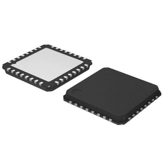
ICGOO电子元器件商城为您提供LAN8710AI-EZK由Microchip设计生产,在icgoo商城现货销售,并且可以通过原厂、代理商等渠道进行代购。 LAN8710AI-EZK价格参考¥询价-¥询价。MicrochipLAN8710AI-EZK封装/规格:接口 - 驱动器,接收器,收发器, 4/4 Transceiver Full MII, RMII 32-QFN (5x5)。您可以下载LAN8710AI-EZK参考资料、Datasheet数据手册功能说明书,资料中有LAN8710AI-EZK 详细功能的应用电路图电压和使用方法及教程。
Microchip Technology的LAN8710AI-EZK是一款高度集成的低功耗以太网物理层收发器,属于接口类中的驱动器/接收器/收发器产品,主要应用于需要10/100Mbps以太网连接的嵌入式系统。该芯片符合IEEE 802.3标准,支持自动协商、自动交叉(Auto-MDIX)和节能以太网(EEE)功能,适用于对功耗敏感的应用场景。

典型应用场景包括工业自动化设备(如PLC、HMI)、智能家居网关、网络摄像头(IP Camera)、楼宇控制系统、POS终端、医疗监控设备以及物联网(IoT)网关等。其小型化封装(QFN-48)和简化的设计有助于节省PCB空间,适合紧凑型设备设计。此外,LAN8710AI-EZK具备良好的EMI/EMC性能,可在工业级温度范围(-40°C至+85°C)稳定工作,增强了在恶劣环境下的可靠性。

该芯片常与各类微控制器(MCU)或处理器配合使用,通过RMII接口连接MAC层,实现快速稳定的有线网络通信。由于其高集成度(内置时钟恢复、信号调理和10BASE-T/100BASE-TX收发功能),可减少外围元件数量,降低系统成本和设计复杂度。

总之,LAN8710AI-EZK广泛用于需要稳定、低功耗、小体积以太网连接的中低端嵌入式网络设备中,是工业与消费类联网应用的理想选择。
| 参数 | 数值 |
| 产品目录 | 集成电路 (IC)半导体 |
| 描述 | TXRX ETHERNET 10/100 MII/RMII以太网 IC 10/100 Ethernet XCVR w/HPAutoMDIX INDTEMP |
| 产品分类 | |
| 品牌 | Microchip Technology |
| 产品手册 | |
| 产品图片 |
|
| rohs | 符合RoHS无铅 / 符合限制有害物质指令(RoHS)规范要求 |
| 产品系列 | 通信及网络 IC,以太网 IC,Microchip Technology LAN8710AI-EZK- |
| 数据手册 | |
| 产品型号 | LAN8710AI-EZK |
| PCN组件/产地 | http://www.microchip.com/mymicrochip/NotificationDetails.aspx?id=5836&print=view |
| 产品 | Ethernet Transceivers |
| 产品目录页面 | |
| 产品种类 | 以太网 IC |
| 以太网连接类型 | 10/100 Base-T |
| 供应商器件封装 | 32-QFN 裸露焊盘(5x5) |
| 其它名称 | 638-1083 |
| 包装 | 托盘 |
| 协议 | MII,RMII |
| 双工 | 全 |
| 商标 | Microchip Technology |
| 安装类型 | 表面贴装 |
| 安装风格 | SMD/SMT |
| 封装 | Tray |
| 封装/外壳 | 32-VFQFN 裸露焊盘 |
| 封装/箱体 | QFN-32 |
| 工作温度 | -40°C ~ 85°C |
| 工厂包装数量 | 490 |
| 接收器滞后 | - |
| 支持标准 | 802.3, 802.3u |
| 数据速率 | - |
| 最大工作温度 | + 85 C |
| 最小工作温度 | - 40 C |
| 标准包装 | 490 |
| 电压-电源 | 1.6 V ~ 3.6 V |
| 电源电压-最大 | 3.6 V |
| 电源电压-最小 | 1.6 V |
| 类型 | Single Chip PHY Transceiver |
| 驱动器/接收器数 | 4/4 |


- 商务部:美国ITC正式对集成电路等产品启动337调查
- 曝三星4nm工艺存在良率问题 高通将骁龙8 Gen1或转产台积电
- 太阳诱电将投资9.5亿元在常州建新厂生产MLCC 预计2023年完工
- 英特尔发布欧洲新工厂建设计划 深化IDM 2.0 战略
- 台积电先进制程称霸业界 有大客户加持明年业绩稳了
- 达到5530亿美元!SIA预计今年全球半导体销售额将创下新高
- 英特尔拟将自动驾驶子公司Mobileye上市 估值或超500亿美元
- 三星加码芯片和SET,合并消费电子和移动部门,撤换高东真等 CEO
- 三星电子宣布重大人事变动 还合并消费电子和移动部门
- 海关总署:前11个月进口集成电路产品价值2.52万亿元 增长14.8%


PDF Datasheet 数据手册内容提取
LAN8710A/LAN8710Ai Small Footprint MII/RMII 10/100 Ethernet Transceiver with HP Auto-MDIX and ® flexPWR Technology PRODUCT FEATURES Datasheet Highlights Key Benefits (cid:132) Single-Chip Ethernet Physical Layer Transceiver (cid:132) High-Performance 10/100 Ethernet Transceiver (PHY) — Compliant with IEEE802.3/802.3u (Fast Ethernet) (cid:132) Comprehensive flexPWR® Technology — Compliant with ISO 802-3/IEEE 802.3 (10BASE-T) — Loop-back modes — Flexible Power Management Architecture — Auto-negotiation — LVCMOS Variable I/O voltage range: +1.6V to +3.6V — Automatic polarity detection and correction — Integrated 1.2V regulator with disable feature — Link status change wake-up detection (cid:132) HP Auto-MDIX support — Vendor specific register functions (cid:132) Small footprint 32-pin QFN lead-free RoHS compliant — Supports both MII and the reduced pin count RMII package (5 x 5 x 0.9mm height) interfaces (cid:132) Power and I/Os — Various low power modes Target Applications — Integrated power-on reset circuit — Two status LED outputs (cid:132) Set-Top Boxes — Latch-Up Performance Exceeds 150mA per EIA/JESD (cid:132) Networked Printers and Servers 78, Class II — May be used with a single 3.3V supply (cid:132) Test Instrumentation (cid:132) LAN on Motherboard (cid:132) Additional Features — Ability to use a low cost 25Mhz crystal for reduced BOM (cid:132) Embedded Telecom Applications (cid:132) Packaging (cid:132) Video Record/Playback Systems — 32-pin QFN (5x5 mm) Lead-Free RoHS Compliant (cid:132) Cable Modems/Routers package with MII and RMII (cid:132) DSL Modems/Routers (cid:132) Environmental (cid:132) Digital Video Recorders — Extended commercial temperature range (0°C to +85°C) (cid:132) IP and Video Phones — Industrial temperature range version available (cid:132) Wireless Access Points (-40°C to +85°C) (cid:132) Digital Televisions (cid:132) Digital Media Adaptors/Servers (cid:132) Gaming Consoles (cid:132) POE Applications (Refer to SMSC Application Note 17.18) SMSC LAN8710A/LAN8710Ai Revision 1.4 (08-23-12) DATASHEET
Small Footprint MII/RMII 10/100 Ethernet Transceiver with HP Auto-MDIX and flexPWR® Technology Datasheet Order Numbers: LAN8710Ai-EZK for 32-pin QFN lead-free RoHS compliant package (-40 to +85°C temp) LAN8710Ai-EZK-TR for 32-pin QFN lead-free RoHS compliant package (-40 to +85°C temp) LAN8710A-EZC for 32-pin QFN lead-free RoHS compliant package (0 to +85°C temp) LAN8710A-EZC-TR for 32-pin QFN lead-free RoHS compliant package (0 to +85°C temp) TR indicates tape & reel option. Reel size is 4,000. This product meets the halogen maximum concentration values per IEC61249-2-21 For RoHS compliance and environmental information, please visit www.smsc.com/rohs Please contact your SMSC sales representative for additional documentation related to this product such as application notes, anomaly sheets, and design guidelines. Copyright © 2012 SMSC or its subsidiaries. All rights reserved. Circuit diagrams and other information relating to SMSC products are included as a means of illustrating typical applications. Consequently, complete information sufficient for construction purposes is not necessarily given. Although the information has been checked and is believed to be accurate, no responsibility is assumed for inaccuracies. SMSC reserves the right to make changes to specifications and product descriptions at any time without notice. Contact your local SMSC sales office to obtain the latest specifications before placing your product order. The provision of this information does not convey to the purchaser of the described semiconductor devices any licenses under any patent rights or other intellectual property rights of SMSC or others. All sales are expressly conditional on your agreement to the terms and conditions of the most recently dated version of SMSC's standard Terms of Sale Agreement dated before the date of your order (the "Terms of Sale Agreement"). The product may contain design defects or errors known as anomalies which may cause the product's functions to deviate from published specifications. Anomaly sheets are available upon request. SMSC products are not designed, intended, authorized or warranted for use in any life support or other application where product failure could cause or contribute to personal injury or severe property damage. Any and all such uses without prior written approval of an Officer of SMSC and further testing and/or modification will be fully at the risk of the customer. Copies of this document or other SMSC literature, as well as the Terms of Sale Agreement, may be obtained by visiting SMSC’s website at http://www.smsc.com. SMSC is a registered trademark of Standard Microsystems Corporation (“SMSC”). Product names and company names are the trademarks of their respective holders. The Microchip name and logo, and the Microchip logo are registered trademarks of Microchip Technology Incorporated in the U.S.A. and other countries. SMSC DISCLAIMS AND EXCLUDES ANY AND ALL WARRANTIES, INCLUDING WITHOUT LIMITATION ANY AND ALL IMPLIED WARRANTIES OF MERCHANTABILITY, FITNESS FOR A PARTICULAR PURPOSE, TITLE, AND AGAINST INFRINGEMENT AND THE LIKE, AND ANY AND ALL WARRANTIES ARISING FROM ANY COURSE OF DEALING OR USAGE OF TRADE. IN NO EVENT SHALL SMSC BE LIABLE FOR ANY DIRECT, INCIDENTAL, INDIRECT, SPECIAL, PUNITIVE, OR CONSEQUENTIAL DAMAGES; OR FOR LOST DATA, PROFITS, SAVINGS OR REVENUES OF ANY KIND; REGARDLESS OF THE FORM OF ACTION, WHETHER BASED ON CONTRACT; TORT; NEGLIGENCE OF SMSC OR OTHERS; STRICT LIABILITY; BREACH OF WARRANTY; OR OTHERWISE; WHETHER OR NOT ANY REMEDY OF BUYER IS HELD TO HAVE FAILED OF ITS ESSENTIAL PURPOSE, AND WHETHER OR NOT SMSC HAS BEEN ADVISED OF THE POSSIBILITY OF SUCH DAMAGES. Revision 1.4 (08-23-12) 2 SMSC LAN8710A/LAN8710Ai DATASHEET
Small Footprint MII/RMII 10/100 Ethernet Transceiver with HP Auto-MDIX and flexPWR® Technology Datasheet Table of Contents Chapter1 Introduction . . . . . . . . . . . . . . . . . . . . . . . . . . . . . . . . . . . . . . . . . . . . . . . . . . . . . . . 7 1.1 General Terms and Conventions . . . . . . . . . . . . . . . . . . . . . . . . . . . . . . . . . . . . . . . . . . . . . . . . . . . 7 1.2 General Description . . . . . . . . . . . . . . . . . . . . . . . . . . . . . . . . . . . . . . . . . . . . . . . . . . . . . . . . . . . . . 7 Chapter2 Pin Description and Configuration . . . . . . . . . . . . . . . . . . . . . . . . . . . . . . . . . . . . 9 2.1 Pin Assignments. . . . . . . . . . . . . . . . . . . . . . . . . . . . . . . . . . . . . . . . . . . . . . . . . . . . . . . . . . . . . . . 17 2.2 Buffer Types. . . . . . . . . . . . . . . . . . . . . . . . . . . . . . . . . . . . . . . . . . . . . . . . . . . . . . . . . . . . . . . . . . 18 Chapter3 Functional Description . . . . . . . . . . . . . . . . . . . . . . . . . . . . . . . . . . . . . . . . . . . . . 19 3.1 Transceiver. . . . . . . . . . . . . . . . . . . . . . . . . . . . . . . . . . . . . . . . . . . . . . . . . . . . . . . . . . . . . . . . . . . 19 3.1.1 100BASE-TX Transmit . . . . . . . . . . . . . . . . . . . . . . . . . . . . . . . . . . . . . . . . . . . . . . . . . . 19 3.1.2 100BASE-TX Receive. . . . . . . . . . . . . . . . . . . . . . . . . . . . . . . . . . . . . . . . . . . . . . . . . . . 22 3.1.3 10BASE-T Transmit. . . . . . . . . . . . . . . . . . . . . . . . . . . . . . . . . . . . . . . . . . . . . . . . . . . . . 24 3.1.4 10BASE-T Receive . . . . . . . . . . . . . . . . . . . . . . . . . . . . . . . . . . . . . . . . . . . . . . . . . . . . . 25 3.2 Auto-negotiation . . . . . . . . . . . . . . . . . . . . . . . . . . . . . . . . . . . . . . . . . . . . . . . . . . . . . . . . . . . . . . . 26 3.2.1 Parallel Detection . . . . . . . . . . . . . . . . . . . . . . . . . . . . . . . . . . . . . . . . . . . . . . . . . . . . . . 27 3.2.2 Restarting Auto-negotiation. . . . . . . . . . . . . . . . . . . . . . . . . . . . . . . . . . . . . . . . . . . . . . . 27 3.2.3 Disabling Auto-negotiation. . . . . . . . . . . . . . . . . . . . . . . . . . . . . . . . . . . . . . . . . . . . . . . . 28 3.2.4 Half vs. Full Duplex . . . . . . . . . . . . . . . . . . . . . . . . . . . . . . . . . . . . . . . . . . . . . . . . . . . . . 28 3.3 HP Auto-MDIX Support. . . . . . . . . . . . . . . . . . . . . . . . . . . . . . . . . . . . . . . . . . . . . . . . . . . . . . . . . . 29 3.4 MAC Interface. . . . . . . . . . . . . . . . . . . . . . . . . . . . . . . . . . . . . . . . . . . . . . . . . . . . . . . . . . . . . . . . . 30 3.4.1 MII . . . . . . . . . . . . . . . . . . . . . . . . . . . . . . . . . . . . . . . . . . . . . . . . . . . . . . . . . . . . . . . . . . 30 3.4.2 RMII. . . . . . . . . . . . . . . . . . . . . . . . . . . . . . . . . . . . . . . . . . . . . . . . . . . . . . . . . . . . . . . . . 30 3.4.3 MII vs. RMII Configuration. . . . . . . . . . . . . . . . . . . . . . . . . . . . . . . . . . . . . . . . . . . . . . . . 31 3.5 Serial Management Interface (SMI) . . . . . . . . . . . . . . . . . . . . . . . . . . . . . . . . . . . . . . . . . . . . . . . . 33 3.6 Interrupt Management . . . . . . . . . . . . . . . . . . . . . . . . . . . . . . . . . . . . . . . . . . . . . . . . . . . . . . . . . . 34 3.6.1 Primary Interrupt System. . . . . . . . . . . . . . . . . . . . . . . . . . . . . . . . . . . . . . . . . . . . . . . . . 34 3.6.2 Alternate Interrupt System. . . . . . . . . . . . . . . . . . . . . . . . . . . . . . . . . . . . . . . . . . . . . . . . 35 3.7 Configuration Straps. . . . . . . . . . . . . . . . . . . . . . . . . . . . . . . . . . . . . . . . . . . . . . . . . . . . . . . . . . . . 36 3.7.1 PHYAD[2:0]: PHY Address Configuration. . . . . . . . . . . . . . . . . . . . . . . . . . . . . . . . . . . . 36 3.7.2 MODE[2:0]: Mode Configuration. . . . . . . . . . . . . . . . . . . . . . . . . . . . . . . . . . . . . . . . . . . 36 3.7.3 RMIISEL: MII/RMII Mode Configuration . . . . . . . . . . . . . . . . . . . . . . . . . . . . . . . . . . . . . 37 3.7.4 REGOFF: Internal +1.2V Regulator Configuration . . . . . . . . . . . . . . . . . . . . . . . . . . . . . 38 3.7.5 nINTSEL: nINT/TXER/TXD4 Configuration. . . . . . . . . . . . . . . . . . . . . . . . . . . . . . . . . . . 38 3.8 Miscellaneous Functions . . . . . . . . . . . . . . . . . . . . . . . . . . . . . . . . . . . . . . . . . . . . . . . . . . . . . . . . 39 3.8.1 LEDs . . . . . . . . . . . . . . . . . . . . . . . . . . . . . . . . . . . . . . . . . . . . . . . . . . . . . . . . . . . . . . . . 39 3.8.2 Variable Voltage I/O . . . . . . . . . . . . . . . . . . . . . . . . . . . . . . . . . . . . . . . . . . . . . . . . . . . . 40 3.8.3 Power-Down Modes . . . . . . . . . . . . . . . . . . . . . . . . . . . . . . . . . . . . . . . . . . . . . . . . . . . . 40 3.8.4 Isolate Mode . . . . . . . . . . . . . . . . . . . . . . . . . . . . . . . . . . . . . . . . . . . . . . . . . . . . . . . . . . 41 3.8.5 Resets. . . . . . . . . . . . . . . . . . . . . . . . . . . . . . . . . . . . . . . . . . . . . . . . . . . . . . . . . . . . . . . 41 3.8.6 Carrier Sense . . . . . . . . . . . . . . . . . . . . . . . . . . . . . . . . . . . . . . . . . . . . . . . . . . . . . . . . . 41 3.8.7 Collision Detect . . . . . . . . . . . . . . . . . . . . . . . . . . . . . . . . . . . . . . . . . . . . . . . . . . . . . . . . 42 3.8.8 Link Integrity Test . . . . . . . . . . . . . . . . . . . . . . . . . . . . . . . . . . . . . . . . . . . . . . . . . . . . . . 42 3.8.9 Loopback Operation . . . . . . . . . . . . . . . . . . . . . . . . . . . . . . . . . . . . . . . . . . . . . . . . . . . . 42 3.9 Application Diagrams . . . . . . . . . . . . . . . . . . . . . . . . . . . . . . . . . . . . . . . . . . . . . . . . . . . . . . . . . . . 44 3.9.1 Simplified System Level Application Diagram. . . . . . . . . . . . . . . . . . . . . . . . . . . . . . . . . 45 3.9.2 Power Supply Diagram (1.2V Supplied by Internal Regulator) . . . . . . . . . . . . . . . . . . . . 46 3.9.3 Power Supply Diagram (1.2V Supplied by External Source). . . . . . . . . . . . . . . . . . . . . . 47 3.9.4 Twisted-Pair Interface Diagram (Single Power Supply). . . . . . . . . . . . . . . . . . . . . . . . . . 48 3.9.5 Twisted-Pair Interface Diagram (Dual Power Supplies) . . . . . . . . . . . . . . . . . . . . . . . . . 49 SMSC LAN8710A/LAN8710Ai 3 Revision 1.4 (08-23-12) DATASHEET
Small Footprint MII/RMII 10/100 Ethernet Transceiver with HP Auto-MDIX and flexPWR® Technology Datasheet Chapter4 Register Descriptions. . . . . . . . . . . . . . . . . . . . . . . . . . . . . . . . . . . . . . . . . . . . . . . 50 4.1 Register Nomenclature. . . . . . . . . . . . . . . . . . . . . . . . . . . . . . . . . . . . . . . . . . . . . . . . . . . . . . . . . . 50 4.2 Control and Status Registers . . . . . . . . . . . . . . . . . . . . . . . . . . . . . . . . . . . . . . . . . . . . . . . . . . . . . 51 4.2.1 Basic Control Register. . . . . . . . . . . . . . . . . . . . . . . . . . . . . . . . . . . . . . . . . . . . . . . . . . . 52 4.2.2 Basic Status Register . . . . . . . . . . . . . . . . . . . . . . . . . . . . . . . . . . . . . . . . . . . . . . . . . . . 53 4.2.3 PHY Identifier 1 Register. . . . . . . . . . . . . . . . . . . . . . . . . . . . . . . . . . . . . . . . . . . . . . . . . 54 4.2.4 PHY Identifier 2 Register. . . . . . . . . . . . . . . . . . . . . . . . . . . . . . . . . . . . . . . . . . . . . . . . . 55 4.2.5 Auto Negotiation Advertisement Register . . . . . . . . . . . . . . . . . . . . . . . . . . . . . . . . . . . . 56 4.2.6 Auto Negotiation Link Partner Ability Register. . . . . . . . . . . . . . . . . . . . . . . . . . . . . . . . . 57 4.2.7 Auto Negotiation Expansion Register . . . . . . . . . . . . . . . . . . . . . . . . . . . . . . . . . . . . . . . 58 4.2.8 Mode Control/Status Register. . . . . . . . . . . . . . . . . . . . . . . . . . . . . . . . . . . . . . . . . . . . . 59 4.2.9 Special Modes Register. . . . . . . . . . . . . . . . . . . . . . . . . . . . . . . . . . . . . . . . . . . . . . . . . . 60 4.2.10 Symbol Error Counter Register . . . . . . . . . . . . . . . . . . . . . . . . . . . . . . . . . . . . . . . . . . . . 61 4.2.11 Special Control/Status Indications Register. . . . . . . . . . . . . . . . . . . . . . . . . . . . . . . . . . . 62 4.2.12 Interrupt Source Flag Register . . . . . . . . . . . . . . . . . . . . . . . . . . . . . . . . . . . . . . . . . . . . 63 4.2.13 Interrupt Mask Register. . . . . . . . . . . . . . . . . . . . . . . . . . . . . . . . . . . . . . . . . . . . . . . . . . 64 4.2.14 PHY Special Control/Status Register . . . . . . . . . . . . . . . . . . . . . . . . . . . . . . . . . . . . . . . 65 Chapter5 Operational Characteristics . . . . . . . . . . . . . . . . . . . . . . . . . . . . . . . . . . . . . . . . . 66 5.1 Absolute Maximum Ratings*. . . . . . . . . . . . . . . . . . . . . . . . . . . . . . . . . . . . . . . . . . . . . . . . . . . . . . 66 5.2 Operating Conditions**. . . . . . . . . . . . . . . . . . . . . . . . . . . . . . . . . . . . . . . . . . . . . . . . . . . . . . . . . . 67 5.3 Power Consumption. . . . . . . . . . . . . . . . . . . . . . . . . . . . . . . . . . . . . . . . . . . . . . . . . . . . . . . . . . . . 67 5.4 DC Specifications. . . . . . . . . . . . . . . . . . . . . . . . . . . . . . . . . . . . . . . . . . . . . . . . . . . . . . . . . . . . . . 68 5.5 AC Specifications . . . . . . . . . . . . . . . . . . . . . . . . . . . . . . . . . . . . . . . . . . . . . . . . . . . . . . . . . . . . . . 70 5.5.1 Equivalent Test Load. . . . . . . . . . . . . . . . . . . . . . . . . . . . . . . . . . . . . . . . . . . . . . . . . . . . 70 5.5.2 Power Sequence Timing. . . . . . . . . . . . . . . . . . . . . . . . . . . . . . . . . . . . . . . . . . . . . . . . . 71 5.5.3 Power-On nRST & Configuration Strap Timing. . . . . . . . . . . . . . . . . . . . . . . . . . . . . . . . 72 5.5.4 MII Interface Timing. . . . . . . . . . . . . . . . . . . . . . . . . . . . . . . . . . . . . . . . . . . . . . . . . . . . . 73 5.5.5 RMII Interface Timing . . . . . . . . . . . . . . . . . . . . . . . . . . . . . . . . . . . . . . . . . . . . . . . . . . . 75 5.5.6 SMI Timing . . . . . . . . . . . . . . . . . . . . . . . . . . . . . . . . . . . . . . . . . . . . . . . . . . . . . . . . . . . 76 5.6 Clock Circuit . . . . . . . . . . . . . . . . . . . . . . . . . . . . . . . . . . . . . . . . . . . . . . . . . . . . . . . . . . . . . . . . . . 77 Chapter6 Package Outline. . . . . . . . . . . . . . . . . . . . . . . . . . . . . . . . . . . . . . . . . . . . . . . . . . . 78 Chapter7 Datasheet Revision History. . . . . . . . . . . . . . . . . . . . . . . . . . . . . . . . . . . . . . . . . . 81 Revision 1.4 (08-23-12) 4 SMSC LAN8710A/LAN8710Ai DATASHEET
Small Footprint MII/RMII 10/100 Ethernet Transceiver with HP Auto-MDIX and flexPWR® Technology Datasheet List of Figures Figure1.1 System Block Diagram. . . . . . . . . . . . . . . . . . . . . . . . . . . . . . . . . . . . . . . . . . . . . . . . . . . . . . . 8 Figure1.2 Architectural Overview. . . . . . . . . . . . . . . . . . . . . . . . . . . . . . . . . . . . . . . . . . . . . . . . . . . . . . . 8 Figure2.1 32-QFN Pin Assignments (TOP VIEW) . . . . . . . . . . . . . . . . . . . . . . . . . . . . . . . . . . . . . . . . . . 9 Figure3.1 100BASE-TX Transmit Data Path . . . . . . . . . . . . . . . . . . . . . . . . . . . . . . . . . . . . . . . . . . . . . 19 Figure3.2 100BASE-TX Receive Data Path. . . . . . . . . . . . . . . . . . . . . . . . . . . . . . . . . . . . . . . . . . . . . . 22 Figure3.3 Relationship Between Received Data and Specific MII Signals . . . . . . . . . . . . . . . . . . . . . . 24 Figure3.4 Direct Cable Connection vs. Cross-over Cable Connection . . . . . . . . . . . . . . . . . . . . . . . . . 29 Figure3.5 MDIO Timing and Frame Structure - READ Cycle. . . . . . . . . . . . . . . . . . . . . . . . . . . . . . . . . 33 Figure3.6 MDIO Timing and Frame Structure - WRITE Cycle. . . . . . . . . . . . . . . . . . . . . . . . . . . . . . . . 33 Figure3.7 LED1/REGOFF Polarity Configuration. . . . . . . . . . . . . . . . . . . . . . . . . . . . . . . . . . . . . . . . . . 39 Figure3.8 LED2/nINTSEL Polarity Configuration. . . . . . . . . . . . . . . . . . . . . . . . . . . . . . . . . . . . . . . . . . 40 Figure3.9 Near-end Loopback Block Diagram. . . . . . . . . . . . . . . . . . . . . . . . . . . . . . . . . . . . . . . . . . . . 43 Figure3.10 Far Loopback Block Diagram. . . . . . . . . . . . . . . . . . . . . . . . . . . . . . . . . . . . . . . . . . . . . . . . . 43 Figure3.11 Connector Loopback Block Diagram . . . . . . . . . . . . . . . . . . . . . . . . . . . . . . . . . . . . . . . . . . . 44 Figure3.12 Simplified System Level Application Diagram . . . . . . . . . . . . . . . . . . . . . . . . . . . . . . . . . . . . 45 Figure3.13 Power Supply Diagram (1.2V Supplied by Internal Regulator) . . . . . . . . . . . . . . . . . . . . . . . 46 Figure3.14 Power Supply Diagram (1.2V Supplied by External Source). . . . . . . . . . . . . . . . . . . . . . . . . 47 Figure3.15 Twisted-Pair Interface Diagram (Single Power Supply). . . . . . . . . . . . . . . . . . . . . . . . . . . . . 48 Figure3.16 Twisted-Pair Interface Diagram (Dual Power Supplies). . . . . . . . . . . . . . . . . . . . . . . . . . . . . 49 Figure5.1 Output Equivalent Test Load . . . . . . . . . . . . . . . . . . . . . . . . . . . . . . . . . . . . . . . . . . . . . . . . . 70 Figure5.2 Power Sequence Timing . . . . . . . . . . . . . . . . . . . . . . . . . . . . . . . . . . . . . . . . . . . . . . . . . . . . 71 Figure5.3 Power-On nRST & Configuration Strap Timing . . . . . . . . . . . . . . . . . . . . . . . . . . . . . . . . . . . 72 Figure5.4 MII Receive Timing . . . . . . . . . . . . . . . . . . . . . . . . . . . . . . . . . . . . . . . . . . . . . . . . . . . . . . . . 73 Figure5.5 MII Transmit Timing. . . . . . . . . . . . . . . . . . . . . . . . . . . . . . . . . . . . . . . . . . . . . . . . . . . . . . . . 74 Figure5.6 RMII Timing . . . . . . . . . . . . . . . . . . . . . . . . . . . . . . . . . . . . . . . . . . . . . . . . . . . . . . . . . . . . . . 75 Figure5.7 SMI Timing. . . . . . . . . . . . . . . . . . . . . . . . . . . . . . . . . . . . . . . . . . . . . . . . . . . . . . . . . . . . . . . 76 Figure6.1 32-QFN Package. . . . . . . . . . . . . . . . . . . . . . . . . . . . . . . . . . . . . . . . . . . . . . . . . . . . . . . . . . 78 Figure6.2 Recommended PCB Land Pattern. . . . . . . . . . . . . . . . . . . . . . . . . . . . . . . . . . . . . . . . . . . . . 79 Figure6.3 Taping Dimensions and Part Orientation. . . . . . . . . . . . . . . . . . . . . . . . . . . . . . . . . . . . . . . . 79 Figure6.4 Reel Dimensions . . . . . . . . . . . . . . . . . . . . . . . . . . . . . . . . . . . . . . . . . . . . . . . . . . . . . . . . . . 80 Figure6.5 Tape Length and Part Quantity . . . . . . . . . . . . . . . . . . . . . . . . . . . . . . . . . . . . . . . . . . . . . . . 80 SMSC LAN8710A/LAN8710Ai 5 Revision 1.4 (08-23-12) DATASHEET
Small Footprint MII/RMII 10/100 Ethernet Transceiver with HP Auto-MDIX and flexPWR® Technology Datasheet List of Tables Table2.1 MII/RMII Signals . . . . . . . . . . . . . . . . . . . . . . . . . . . . . . . . . . . . . . . . . . . . . . . . . . . . . . . . . . . 10 Table2.2 LED Pins . . . . . . . . . . . . . . . . . . . . . . . . . . . . . . . . . . . . . . . . . . . . . . . . . . . . . . . . . . . . . . . . . 13 Table2.3 Serial Management Interface (SMI) Pins. . . . . . . . . . . . . . . . . . . . . . . . . . . . . . . . . . . . . . . . . 14 Table2.4 Ethernet Pins. . . . . . . . . . . . . . . . . . . . . . . . . . . . . . . . . . . . . . . . . . . . . . . . . . . . . . . . . . . . . . 14 Table2.5 Miscellaneous Pins . . . . . . . . . . . . . . . . . . . . . . . . . . . . . . . . . . . . . . . . . . . . . . . . . . . . . . . . . 15 Table2.6 Analog Reference Pins . . . . . . . . . . . . . . . . . . . . . . . . . . . . . . . . . . . . . . . . . . . . . . . . . . . . . . 15 Table2.7 Power Pins. . . . . . . . . . . . . . . . . . . . . . . . . . . . . . . . . . . . . . . . . . . . . . . . . . . . . . . . . . . . . . . . 16 Table2.8 32-QFN Package Pin Assignments. . . . . . . . . . . . . . . . . . . . . . . . . . . . . . . . . . . . . . . . . . . . . 17 Table2.9 Buffer Types . . . . . . . . . . . . . . . . . . . . . . . . . . . . . . . . . . . . . . . . . . . . . . . . . . . . . . . . . . . . . . 18 Table3.1 4B/5B Code Table. . . . . . . . . . . . . . . . . . . . . . . . . . . . . . . . . . . . . . . . . . . . . . . . . . . . . . . . . . 20 Table3.2 MII/RMII Signal Mapping. . . . . . . . . . . . . . . . . . . . . . . . . . . . . . . . . . . . . . . . . . . . . . . . . . . . . 32 Table3.3 Interrupt Management Table. . . . . . . . . . . . . . . . . . . . . . . . . . . . . . . . . . . . . . . . . . . . . . . . . . 34 Table3.4 Alternative Interrupt System Management Table . . . . . . . . . . . . . . . . . . . . . . . . . . . . . . . . . . 35 Table3.5 Pin Names for Address Bits. . . . . . . . . . . . . . . . . . . . . . . . . . . . . . . . . . . . . . . . . . . . . . . . . . . 36 Table3.6 MODE[2:0] Bus . . . . . . . . . . . . . . . . . . . . . . . . . . . . . . . . . . . . . . . . . . . . . . . . . . . . . . . . . . . . 37 Table3.7 Pin Names for Mode Bits. . . . . . . . . . . . . . . . . . . . . . . . . . . . . . . . . . . . . . . . . . . . . . . . . . . . . 37 Table4.1 Register Bit Types. . . . . . . . . . . . . . . . . . . . . . . . . . . . . . . . . . . . . . . . . . . . . . . . . . . . . . . . . . 50 Table4.2 SMI Register Map . . . . . . . . . . . . . . . . . . . . . . . . . . . . . . . . . . . . . . . . . . . . . . . . . . . . . . . . . . 51 Table5.1 Device Only Current Consumption and Power Dissipation. . . . . . . . . . . . . . . . . . . . . . . . . . . 67 Table5.2 Non-Variable I/O Buffer Characteristics. . . . . . . . . . . . . . . . . . . . . . . . . . . . . . . . . . . . . . . . . . 68 Table5.3 Variable I/O Buffer Characteristics . . . . . . . . . . . . . . . . . . . . . . . . . . . . . . . . . . . . . . . . . . . . . 69 Table5.4 100BASE-TX Transceiver Characteristics. . . . . . . . . . . . . . . . . . . . . . . . . . . . . . . . . . . . . . . . 69 Table5.5 10BASE-T Transceiver Characteristics. . . . . . . . . . . . . . . . . . . . . . . . . . . . . . . . . . . . . . . . . . 70 Table5.6 Power Sequence Timing Values . . . . . . . . . . . . . . . . . . . . . . . . . . . . . . . . . . . . . . . . . . . . . . . 71 Table5.7 Power-On nRST & Configuration Strap Timing Values. . . . . . . . . . . . . . . . . . . . . . . . . . . . . . 72 Table5.8 MII Receive Timing Values . . . . . . . . . . . . . . . . . . . . . . . . . . . . . . . . . . . . . . . . . . . . . . . . . . . 73 Table5.9 MII Transmit Timing Values. . . . . . . . . . . . . . . . . . . . . . . . . . . . . . . . . . . . . . . . . . . . . . . . . . . 74 Table5.10RMII Timing Values . . . . . . . . . . . . . . . . . . . . . . . . . . . . . . . . . . . . . . . . . . . . . . . . . . . . . . . . 75 Table5.11RMII CLKIN (REF_CLK) Timing Values . . . . . . . . . . . . . . . . . . . . . . . . . . . . . . . . . . . . . . . . . 76 Table5.12SMI Timing Values. . . . . . . . . . . . . . . . . . . . . . . . . . . . . . . . . . . . . . . . . . . . . . . . . . . . . . . . . . 76 Table5.13Crystal Specifications . . . . . . . . . . . . . . . . . . . . . . . . . . . . . . . . . . . . . . . . . . . . . . . . . . . . . . . 77 Table6.1 32-QFN Dimensions . . . . . . . . . . . . . . . . . . . . . . . . . . . . . . . . . . . . . . . . . . . . . . . . . . . . . . . . 78 Table7.1 Customer Revision History . . . . . . . . . . . . . . . . . . . . . . . . . . . . . . . . . . . . . . . . . . . . . . . . . . . 81 Revision 1.4 (08-23-12) 6 SMSC LAN8710A/LAN8710Ai DATASHEET
Small Footprint MII/RMII 10/100 Ethernet Transceiver with HP Auto-MDIX and flexPWR® Technology Datasheet Chapter 1 Introduction 1.1 General Terms and Conventions The following is list of the general terms used throughout this document: BYTE 8-bits FIFO First In First Out buffer; often used for elasticity buffer MAC Media Access Controller MII Media Independent Interface RMIITM Reduced Media Independent InterfaceTM N/A Not Applicable X Indicates that a logic state is “don’t care” or undefined. RESERVED Refers to a reserved bit field or address. Unless otherwise noted, reserved bits must always be zero for write operations. Unless otherwise noted, values are not guaranteed when reading reserved bits. Unless otherwise noted, do not read or write to reserved addresses. SMI Serial Management Interface 1.2 General Description The LAN8710A/LAN8710Ai is a low-power 10BASE-T/100BASE-TX physical layer (PHY) transceiver with variable I/O voltage that is compliant with the IEEE 802.3-2005 standards. The LAN8710A/LAN8710Ai supports communication with an Ethernet MAC via a standard MII (IEEE 802.3u)/RMII interface. It contains a full-duplex 10-BASE-T/100BASE-TX transceiver and supports 10Mbps (10BASE-T) and 100Mbps (100BASE-TX) operation. The LAN8710A/LAN8710Ai implements auto-negotiation to automatically determine the best possible speed and duplex mode of operation. HP Auto-MDIX support allows the use of direct connect or cross-over LAN cables. The LAN8710A/LAN8710Ai supports both IEEE 802.3-2005 compliant and vendor-specific register functions. However, no register access is required for operation. The initial configuration may be selected via the configuration pins as described in Section 3.7, "Configuration Straps," on page36. Register-selectable configuration options may be used to further define the functionality of the transceiver. Per IEEE 802.3-2005 standards, all digital interface pins are tolerant to 3.6V. The device can be configured to operate on a single 3.3V supply utilizing an integrated 3.3V to 1.2V linear regulator. The linear regulator may be optionally disabled, allowing usage of a high efficiency external regulator for lower system power dissipation. The LAN8710A/LAN8710Ai is available in both extended commercial and industrial temperature range versions. A typical system application is shown in Figure1.1. SMSC LAN8710A/LAN8710Ai 7 Revision 1.4 (08-23-12) DATASHEET
Small Footprint MII/RMII 10/100 Ethernet Transceiver with HP Auto-MDIX and flexPWR® Technology Datasheet 10/100 MII/ Ethernet RMII LAN8710A/ MDI Transformer RJ45 LAN8710Ai MAC Mode LED Crystal or Clock Oscillator Figure1.1 System Block Diagram MODE[0:2] Mode Control HP Auto-MDIX Auto- 100M TX 100M TXP/TXN nRST Reset Control Negotiation Logic Transmitter Transmitter RXP/RXN RMIISEL TXD[0:3] SMI Management 10M TX 10M MDIX TXEN Control Logic Transmitter Control TXER XTAL1/CLKIN TXCLK PLL XTAL2 RXD[0:3] c gi RXDV Lo 100M RX DSP System: Analog-to- Interrupt nINT RXER MII Logic DataC Rloecckovery Digital Generator RXCLK MII/ Equalizer 100M PLL LED1 R LEDs CRS Receiver LED2 COL/CRS_DV 10M RX Squeltch MDC Logic & Filters Central Bias RBIAS 10M PLL MDIO PHY Address PHYAD[0:2] Latches LAN8710A/LAN8710Ai Figure1.2 Architectural Overview Revision 1.4 (08-23-12) 8 SMSC LAN8710A/LAN8710Ai DATASHEET
Small Footprint MII/RMII 10/100 Ethernet Transceiver with HP Auto-MDIX and flexPWR® Technology Datasheet Chapter 2 Pin Description and Configuration 4 D X T R/ E X K T XD2 XD1 XD0 XEN XCL RST NT/ DC T T T T T n nI M 4 3 2 1 0 9 8 7 2 2 2 2 2 1 1 1 TXD3 25 16 MDIO SMSC RXDV 26 15 COL/CRS_DV/MODE2 LAN8710A/LAN8710Ai VDD1A 27 32 PIN QFN 14 CRS (TOP VIEW) TXN 28 13 RXER/RXD4/PHYAD0 VSS TXP 29 12 VDDIO RXN 30 11 RXD0/MODE0 RXP 31 10 RXD1/MODE1 RBIAS 32 9 RXD2/RMIISEL 1 2 3 4 5 6 7 8 A L F 2 N R 1 2 VDD2 2/nINTSE 1/REGOF XTAL AL1/CLKI VDDC K/PHYAD 3/PHYAD D D T L D E E X C X L L X R R NOTE: Exposed pad (VSS) on bottom of package must be connected to ground Figure2.1 32-QFN Pin Assignments (TOP VIEW) Note: When a lower case “n” is used at the beginning of the signal name, it indicates that the signal is active low. For example, nRST indicates that the reset signal is active low. Note: The buffer type for each signal is indicated in the BUFFER TYPE column. A description of the buffer types is provided in Section2.2. SMSC LAN8710A/LAN8710Ai 9 Revision 1.4 (08-23-12) DATASHEET
Small Footprint MII/RMII 10/100 Ethernet Transceiver with HP Auto-MDIX and flexPWR® Technology Datasheet Table2.1 MII/RMII Signals BUFFER NUM PINS NAME SYMBOL TYPE DESCRIPTION Transmit TXD0 VIS The MAC transmits data to the transceiver using 1 Data 0 this signal in all modes. Transmit TXD1 VIS The MAC transmits data to the transceiver using 1 Data 1 this signal in all modes. Transmit TXD2 VIS The MAC transmits data to the transceiver using Data 2 this signal in MII Mode. 1 (MII Mode) Note: This signal must be grounded in RMII Mode. Transmit TXD3 VIS The MAC transmits data to the transceiver using Data 3 this signal in MII Mode. 1 (MII Mode) Note: This signal must be grounded in RMII Mode. Interrupt nINT VO8 Active low interrupt output. Place an external Output resistor pull-up to VDDIO. Note: Refer to Section 3.6, "Interrupt Management," on page34 for additional details on device interrupts. Note: Refer to Section 3.8.1.2, "nINTSEL and LED2 Polarity Selection," on page39 for details on how the nINTSEL configuration strap is used to determine 1 the function of this pin. Transmit TXER VIS When driven high, the 4B/5B encode process Error (PU) substitutes the Transmit Error code-group (/H/) (MII Mode) for the encoded data word. This input is ignored in the 10BASE-T mode of operation. Transmit TXD4 VIS In Symbol Interface (5B Decoding) mode, this Data 4 (PU) signal becomes the MII Transmit Data 4 line (the (MII Mode) MSB of the 5-bit symbol code-group). Note: This signal is not used in RMII Mode. Transmit TXEN VIS Indicates that valid transmission data is present 1 Enable (PD) on TXD[3:0]. In RMII Mode, only TXD[1:0] provide valid data. Transmit TXCLK VO8 Used to latch data from the MAC into the Clock transceiver. 1 (MII Mode) (cid:132)MII (100BASE-TX): 25MHz (cid:132)MII (10BASE-T): 2.5MHz Note: This signal is not used in RMII Mode. Revision 1.4 (08-23-12) 10 SMSC LAN8710A/LAN8710Ai DATASHEET
Small Footprint MII/RMII 10/100 Ethernet Transceiver with HP Auto-MDIX and flexPWR® Technology Datasheet Table2.1 MII/RMII Signals (continued) BUFFER NUM PINS NAME SYMBOL TYPE DESCRIPTION Receive RXD0 VO8 Bit 0 of the 4 (2 in RMII Mode) data bits that are Data 0 sent by the transceiver on the receive path. PHY MODE0 VIS Combined with MODE1 and MODE2, this Operating (PU) configuration strap sets the default PHY mode. 1 Mode 0 Configuration See Note2.1 for more information on configuration straps. Strap Note: Refer to Section 3.7.2, "MODE[2:0]: Mode Configuration," on page36 for additional details. Receive RXD1 VO8 Bit 1 of the 4 (2 in RMII Mode) data bits that are Data 1 sent by the transceiver on the receive path. PHY MODE1 VIS Combined with MODE0 and MODE2, this Operating (PU) configuration strap sets the default PHY mode. 1 Mode 1 See Note2.1 for more information on Configuration configuration straps. Strap Note: Refer to Section 3.7.2, "MODE[2:0]: Mode Configuration," on page36 for additional details. Receive RXD2 VO8 Bit 2 of the 4 (in MII Mode) data bits that are sent Data 2 by the transceiver on the receive path. (MII Mode) Note: This signal is not used in RMII Mode. MII/RMII RMIISEL VIS This configuration strap selects the MII or RMII Mode Select (PD) mode of operation. When strapped low to VSS, Configuration MII Mode is selected. When strapped high to 1 Strap VDDIO RMII Mode is selected. See Note2.1 for more information on configuration straps. Note: Refer to Section 3.7.3, "RMIISEL: MII/RMII Mode Configuration," on page37 for additional details. Receive RXD3 VO8 Bit 3 of the 4 (in MII Mode) data bits that are sent Data 3 by the transceiver on the receive path. (MII Mode) Note: This signal is not used in RMII Mode. PHY Address PHYAD2 VIS Combined with PHYAD0 and PHYAD1, this 2 (PD) configuration strap sets the transceiver’s SMI 1 Configuration address. Strap See Note2.1 for more information on configuration straps. Note: Refer to Section 3.7.1, "PHYAD[2:0]: PHY Address Configuration," on page36 for additional information. SMSC LAN8710A/LAN8710Ai 11 Revision 1.4 (08-23-12) DATASHEET
Small Footprint MII/RMII 10/100 Ethernet Transceiver with HP Auto-MDIX and flexPWR® Technology Datasheet Table2.1 MII/RMII Signals (continued) BUFFER NUM PINS NAME SYMBOL TYPE DESCRIPTION Receive Error RXER VO8 This signal is asserted to indicate that an error was detected somewhere in the frame presently being transferred from the transceiver. Note: This signal is optional in RMII Mode. Receive RXD4 VO8 In Symbol Interface (5B Decoding) mode, this Data 4 signal is the MII Receive Data 4 signal, the MSB (MII Mode) of the received 5-bit symbol code-group. Note: Unless configured to the Symbol 1 Interface mode, this pin functions as RXER. PHY Address PHYAD0 VIS Combined with PHYAD1 and PHYAD2, this 0 (PD) configuration strap sets the transceiver’s SMI Configuration address. Strap See Note2.1 for more information on configuration straps. Note: Refer to Section 3.7.1, "PHYAD[2:0]: PHY Address Configuration," on page36 for additional information. Receive RXCLK VO8 In MII mode, this pin is the receive clock output. Clock (cid:132)MII (100BASE-TX): 25MHz (MII Mode) (cid:132)MII (10BASE-T): 2.5MHz PHY Address PHYAD1 VIS Combined with PHYAD0 and PHYAD2, this 1 (PD) configuration strap sets the transceiver’s SMI 1 Configuration address. Strap See Note2.1 for more information on configuration straps. Note: Refer to Section 3.7.1, "PHYAD[2:0]: PHY Address Configuration," on page36 for additional information. Receive Data RXDV VO8 Indicates that recovered and decoded data is 1 Valid available on the RXD pins. Revision 1.4 (08-23-12) 12 SMSC LAN8710A/LAN8710Ai DATASHEET
Small Footprint MII/RMII 10/100 Ethernet Transceiver with HP Auto-MDIX and flexPWR® Technology Datasheet Table2.1 MII/RMII Signals (continued) BUFFER NUM PINS NAME SYMBOL TYPE DESCRIPTION Carrier Sense CRS_DV VO8 This signal is asserted to indicate the receive / Receive medium is non-idle in RMII Mode. When a Data Valid 10BASE-T packet is received, CRS_DV is (RMII Mode) asserted, but RXD[1:0] is held low until the SFD byte (10101011) is received. Note: Per the RMII standard, transmitted data is not looped back onto the receive data pins in 10BASE-T half-duplex mode. Collision COL VO8 This signal is asserted to indicate detection of a 1 Detect collision condition in MII Mode. (MII Mode) PHY MODE2 VIS Combined with MODE0 and MODE1, this Operating (PU) configuration strap sets the default PHY mode. Mode 2 Configuration See Note2.1 for more information on configuration straps. Strap Note: Refer to Section 3.7.2, "MODE[2:0]: Mode Configuration," on page36 for additional details. Carrier Sense CRS VO8 This signal indicates detection of a carrier in MII 1 (MII Mode) (PD) Mode. Note2.1 Configuration strap values are latched on power-on reset and system reset. Configuration straps are identified by an underlined symbol name. Signals that function as configuration straps must be augmented with an external resistor when connected to a load. Refer to Section 3.7, "Configuration Straps," on page36 for additional information. Table2.2 LED Pins BUFFER NUM PINS NAME SYMBOL TYPE DESCRIPTION LED 1 LED1 O12 Link activity LED Indication. This pin is driven active when a valid link is detected and blinks when activity is detected. Note: Refer to Section 3.8.1, "LEDs," on page39 for additional LED information. Regulator Off REGOFF IS This configuration strap is used to disable the Configuration (PD) internal 1.2V regulator. When the regulator is Strap disabled, external 1.2V must be supplied to VDDCR. 1 (cid:132)When REGOFF is pulled high to VDD2A with an external resistor, the internal regulator is disabled. (cid:132)When REGOFF is floating or pulled low, the internal regulator is enabled (default). See Note2.2 for more information on configuration straps. Note: Refer to Section 3.7.4, "REGOFF: Internal +1.2V Regulator Configuration," on page38 for additional details. SMSC LAN8710A/LAN8710Ai 13 Revision 1.4 (08-23-12) DATASHEET
Small Footprint MII/RMII 10/100 Ethernet Transceiver with HP Auto-MDIX and flexPWR® Technology Datasheet Table2.2 LED Pins (continued) BUFFER NUM PINS NAME SYMBOL TYPE DESCRIPTION LED 2 LED2 O12 Link Speed LED Indication. This pin is driven active when the operating speed is 100Mbps. It is inactive when the operating speed is 10Mbps or during line isolation. Note: Refer to Section 3.8.1, "LEDs," on page39 for additional LED information. nINT/TXER/ nINTSEL IS This configuration strap selects the mode of the TXD4 (PU) nINT/TXER/TXD4 pin. Function Select (cid:132)When nINTSEL is floated or pulled to VDD2A, 1 Configuration nINT is selected for operation on the Strap nINT/TXER/TXD4 pin (default). (cid:132)When nINTSEL is pulled low to VSS, TXER/TXD4 is selected for operation on the nINT/TXER/TXD4 pin. See Note2.2 for more information on configuration straps. Note: Refer to See Section 3.8.1.2, "nINTSEL and LED2 Polarity Selection," on page39 for additional information. Note2.2 Configuration strap values are latched on power-on reset and system reset. Configuration straps are identified by an underlined symbol name. Signals that function as configuration straps must be augmented with an external resistor when connected to a load. Refer to Section 3.7, "Configuration Straps," on page36 for additional information. Table2.3 Serial Management Interface (SMI) Pins BUFFER NUM PINS NAME SYMBOL TYPE DESCRIPTION SMI Data MDIO VIS/ Serial Management Interface data input/output 1 Input/Output VOD8 1 SMI Clock MDC VIS Serial Management Interface clock Table2.4 Ethernet Pins BUFFER NUM PINS NAME SYMBOL TYPE DESCRIPTION Ethernet TXP AIO Transmit/Receive Positive Channel 1 TX/RX 1 Positive Channel 1 Ethernet TXN AIO Transmit/Receive Negative Channel 1 TX/RX 1 Negative Channel 1 Revision 1.4 (08-23-12) 14 SMSC LAN8710A/LAN8710Ai DATASHEET
Small Footprint MII/RMII 10/100 Ethernet Transceiver with HP Auto-MDIX and flexPWR® Technology Datasheet Table2.4 Ethernet Pins (continued) BUFFER NUM PINS NAME SYMBOL TYPE DESCRIPTION Ethernet RXP AIO Transmit/Receive Positive Channel 2 TX/RX 1 Positive Channel 2 Ethernet RXN AIO Transmit/Receive Negative Channel 2 TX/RX 1 Negative Channel 2 Table2.5 Miscellaneous Pins BUFFER NUM PINS NAME SYMBOL TYPE DESCRIPTION External XTAL1 ICLK External crystal input Crystal Input 1 External CLKIN ICLK Single-ended clock oscillator input. Clock Input Note: When using a single ended clock oscillator, XTAL2 should be left unconnected. External XTAL2 OCLK External crystal output 1 Crystal Output External nRST VIS System reset. This signal is active low. 1 Reset (PU) Table2.6 Analog Reference Pins BUFFER NUM PINS NAME SYMBOL TYPE DESCRIPTION External 1% RBIAS AI This pin requires connection of a 12.1k ohm (1%) Bias Resistor resistor to ground. Input Refer to the LAN8710A/LAN8710Ai reference 1 schematic for connection information. Note: The nominal voltage is 1.2V and the resistor will dissipate approximately 1mW of power. SMSC LAN8710A/LAN8710Ai 15 Revision 1.4 (08-23-12) DATASHEET
Small Footprint MII/RMII 10/100 Ethernet Transceiver with HP Auto-MDIX and flexPWR® Technology Datasheet Table2.7 Power Pins BUFFER NUM PINS NAME SYMBOL TYPE DESCRIPTION +1.6V to VDDIO P +1.6V to +3.6V variable I/O power +3.6V 1 Variable I/O Refer to the LAN8710A/LAN8710Ai reference Power schematic for connection information. +1.2V Digital VDDCR P Supplied by the on-chip regulator unless Core Power configured for regulator off mode via the Supply REGOFF configuration strap. Refer to the LAN8710A/LAN8710Ai reference 1 schematic for connection information. Note: 1 uF and 470 pF decoupling capacitors in parallel to ground should be used on this pin. +3.3V VDD1A P +3.3V Analog Port Power to Channel 1 Channel 1 1 Analog Port Refer to the LAN8710A/LAN8710Ai reference Power schematic for connection information. +3.3V VDD2A P +3.3V Analog Port Power to Channel 2 and the Channel 2 internal regulator. 1 Analog Port Power Refer to the LAN8710A/LAN8710Ai reference schematic for connection information. Ground VSS P Common ground. This exposed pad must be 1 connected to the ground plane with a via array. Revision 1.4 (08-23-12) 16 SMSC LAN8710A/LAN8710Ai DATASHEET
Small Footprint MII/RMII 10/100 Ethernet Transceiver with HP Auto-MDIX and flexPWR® Technology Datasheet 2.1 Pin Assignments Table2.8 32-QFN Package Pin Assignments PIN NUM PIN NAME PIN NUM PIN NAME 1 VDD2A 17 MDC 2 LED2/nINTSEL 18 nINT/TXER/TXD4 3 LED1/REGOFF 19 nRST 4 XTAL2 20 TXCLK 5 XTAL1/CLKIN 21 TXEN 6 VDDCR 22 TXD0 7 RXCLK/PHYAD1 23 TXD1 8 RXD3/PHYAD2 24 TXD2 9 RXD2/RMIISEL 25 TXD3 10 RXD1/MODE1 26 RXDV 11 RXD0/MODE0 27 VDD1A 12 VDDIO 28 TXN 13 RXER/RXD4/PHYAD0 29 TXP 14 CRS 30 RXN 15 COL/CRS_DV/MODE2 31 RXP 16 MDIO 32 RBIAS SMSC LAN8710A/LAN8710Ai 17 Revision 1.4 (08-23-12) DATASHEET
Small Footprint MII/RMII 10/100 Ethernet Transceiver with HP Auto-MDIX and flexPWR® Technology Datasheet 2.2 Buffer Types Table2.9 Buffer Types BUFFER TYPE DESCRIPTION IS Schmitt-triggered input O12 Output with 12mA sink and 12mA source VIS Variable voltage Schmitt-triggered input VO8 Variable voltage output with 8mA sink and 8mA source VOD8 Variable voltage open-drain output with 8mA sink PU 50uA (typical) internal pull-up. Unless otherwise noted in the pin description, internal pull- ups are always enabled. Note: Internal pull-up resistors prevent unconnected inputs from floating. Do not rely on internal resistors to drive signals external to the device. When connected to a load that must be pulled high, an external resistor must be added. PD 50uA (typical) internal pull-down. Unless otherwise noted in the pin description, internal pull-downs are always enabled. Note: Internal pull-down resistors prevent unconnected inputs from floating. Do not rely on internal resistors to drive signals external to the device. When connected to a load that must be pulled low, an external resistor must be added. AI Analog input AIO Analog bi-directional ICLK Crystal oscillator input pin OCLK Crystal oscillator output pin P Power pin Note: The digital signals are not 5V tolerant. Refer to Section 5.1, "Absolute Maximum Ratings*," on page66 for additional buffer information. Note2.3 Sink and source capabilities are dependant on the VDDIO voltage. Refer to Section 5.1, "Absolute Maximum Ratings*," on page66 for additional information. Revision 1.4 (08-23-12) 18 SMSC LAN8710A/LAN8710Ai DATASHEET
Small Footprint MII/RMII 10/100 Ethernet Transceiver with HP Auto-MDIX and flexPWR® Technology Datasheet Chapter 3 Functional Description This chapter provides functional descriptions of the various device features. These features have been categorized into the following sections: (cid:132) Transceiver (cid:132) Auto-negotiation (cid:132) HP Auto-MDIX Support (cid:132) MAC Interface (cid:132) Serial Management Interface (SMI) (cid:132) Interrupt Management (cid:132) Configuration Straps (cid:132) Miscellaneous Functions (cid:132) Application Diagrams 3.1 Transceiver 3.1.1 100BASE-TX Transmit The 100BASE-TX transmit data path is shown in Figure3.1. Each major block is explained in the following subsections. TX_CLK (for MII only) PLL MAC Ext Ref_CLK (for RMII only) MII 25 Mhz by 4 bits 25MHz 4B/5B 25MHz by Scrambler or MII/RMII by 4 bits Encoder 5 bits and PISO RMII 50Mhz by 2 bits NRZI MLT-3 Tx 125 Mbps Serial NRZI MLT-3 Converter Converter Driver MLT-3 Magnetics MLT-3 RJ45 MLT-3 CAT-5 Figure3.1 100BASE-TX Transmit Data Path 3.1.1.1 100BASE-TX Transmit Data Across the MII/RMII Interface For MII, the MAC controller drives the transmit data onto the TXD bus and asserts TXEN to indicate valid data. The data is latched by the transceiver’s MII block on the rising edge of TXCLK. The data is in the form of 4-bit wide 25MHz data. SMSC LAN8710A/LAN8710Ai 19 Revision 1.4 (08-23-12) DATASHEET
Small Footprint MII/RMII 10/100 Ethernet Transceiver with HP Auto-MDIX and flexPWR® Technology Datasheet For RMII, the MAC controller drives the transmit data onto the TXD bus and asserts TXEN to indicate valid data. The data is latched by the transceiver’s RMII block on the rising edge of REF_CLK. The data is in the form of 2-bit wide 50MHz data. 3.1.1.2 4B/5B Encoding The transmit data passes from the MII/RMII block to the 4B/5B encoder. This block encodes the data from 4-bit nibbles to 5-bit symbols (known as “code-groups”) according to Table3.1. Each 4-bit data- nibble is mapped to 16 of the 32 possible code-groups. The remaining 16 code-groups are either used for control information or are not valid. The first 16 code-groups are referred to by the hexadecimal values of their corresponding data nibbles, 0 through F. The remaining code-groups are given letter designations with slashes on either side. For example, an IDLE code-group is /I/, a transmit error code-group is /H/, etc. Table3.1 4B/5B Code Table CODE RECEIVER TRANSMITTER GROUP SYM INTERPRETATION INTERPRETATION 11110 0 0 0000 DATA 0 0000 DATA 01001 1 1 0001 1 0001 10100 2 2 0010 2 0010 10101 3 3 0011 3 0011 01010 4 4 0100 4 0100 01011 5 5 0101 5 0101 01110 6 6 0110 6 0110 01111 7 7 0111 7 0111 10010 8 8 1000 8 1000 10011 9 9 1001 9 1001 10110 A A 1010 A 1010 10111 B B 1011 B 1011 11010 C C 1100 C 1100 11011 D D 1101 D 1101 11100 E E 1110 E 1110 11101 F F 1111 F 1111 11111 I IDLE Sent after /T/R until TXEN 11000 J First nibble of SSD, translated to “0101” Sent for rising TXEN following IDLE, else RXER 10001 K Second nibble of SSD, translated to Sent for rising TXEN “0101” following J, else RXER 01101 T First nibble of ESD, causes de-assertion Sent for falling TXEN of CRS if followed by /R/, else assertion of RXER Revision 1.4 (08-23-12) 20 SMSC LAN8710A/LAN8710Ai DATASHEET
Small Footprint MII/RMII 10/100 Ethernet Transceiver with HP Auto-MDIX and flexPWR® Technology Datasheet Table3.1 4B/5B Code Table (continued) CODE RECEIVER TRANSMITTER GROUP SYM INTERPRETATION INTERPRETATION 00111 R Second nibble of ESD, causes Sent for falling TXEN deassertion of CRS if following /T/, else assertion of RXER 00100 H Transmit Error Symbol Sent for rising TXER 00110 V INVALID, RXER if during RXDV INVALID 11001 V INVALID, RXER if during RXDV INVALID 00000 V INVALID, RXER if during RXDV INVALID 00001 V INVALID, RXER if during RXDV INVALID 00010 V INVALID, RXER if during RXDV INVALID 00011 V INVALID, RXER if during RXDV INVALID 00101 V INVALID, RXER if during RXDV INVALID 01000 V INVALID, RXER if during RXDV INVALID 01100 V INVALID, RXER if during RXDV INVALID 10000 V INVALID, RXER if during RXDV INVALID 3.1.1.3 Scrambling Repeated data patterns (especially the IDLE code-group) can have power spectral densities with large narrow-band peaks. Scrambling the data helps eliminate these peaks and spread the signal power more uniformly over the entire channel bandwidth. This uniform spectral density is required by FCC regulations to prevent excessive EMI from being radiated by the physical wiring. The seed for the scrambler is generated from the transceiver address, PHYAD, ensuring that in multiple-transceiver applications, such as repeaters or switches, each transceiver will have its own scrambler sequence. The scrambler also performs the Parallel In Serial Out conversion (PISO) of the data. 3.1.1.4 NRZI and MLT-3 Encoding The scrambler block passes the 5-bit wide parallel data to the NRZI converter where it becomes a serial 125MHz NRZI data stream. The NRZI is encoded to MLT-3. MLT-3 is a tri-level code where a change in the logic level represents a code bit “1” and the logic output remaining at the same level represents a code bit “0”. 3.1.1.5 100M Transmit Driver The MLT3 data is then passed to the analog transmitter, which drives the differential MLT-3 signal, on outputs TXP and TXN, to the twisted pair media across a 1:1 ratio isolation transformer. The 10BASE- T and 100BASE-TX signals pass through the same transformer so that common “magnetics” can be used for both. The transmitter drives into the 100Ω impedance of the CAT-5 cable. Cable termination and impedance matching require external components. SMSC LAN8710A/LAN8710Ai 21 Revision 1.4 (08-23-12) DATASHEET
Small Footprint MII/RMII 10/100 Ethernet Transceiver with HP Auto-MDIX and flexPWR® Technology Datasheet 3.1.1.6 100M Phase Lock Loop (PLL) The 100M PLL locks onto reference clock and generates the 125MHz clock used to drive the 125 MHz logic and the 100BASE-TX transmitter. 3.1.2 100BASE-TX Receive The 100BASE-TX receive data path is shown in Figure3.2. Each major block is explained in the following subsections. RX_CLK (for MII only) PLL MAC Ext Ref_CLK (for RMII only) 25MHz 25MHz by MII 25Mhz by 4 bits by 4 bits 4B/5B 5 bits Descrambler or MII/RMII RMII 50Mhz by 2 bits Decoder and SIPO 125 Mbps Serial DSP: Timing NRZI NRZI MLT-3 MLT-3 recovery, Equalizer Converter Converter and BLW Correction A/D MLT-3 MLT-3 MLT-3 Magnetics RJ45 CAT-5 Converter 6 bit Data Figure3.2 100BASE-TX Receive Data Path 3.1.2.1 100M Receive Input The MLT-3 from the cable is fed into the transceiver (on inputs RXP and RXN) via a 1:1 ratio transformer. The ADC samples the incoming differential signal at a rate of 125M samples per second. Using a 64-level quanitizer, it generates 6 digital bits to represent each sample. The DSP adjusts the gain of the ADC according to the observed signal levels such that the full dynamic range of the ADC can be used. 3.1.2.2 Equalizer, Baseline Wander Correction and Clock and Data Recovery The 6 bits from the ADC are fed into the DSP block. The equalizer in the DSP section compensates for phase and amplitude distortion caused by the physical channel consisting of magnetics, connectors, and CAT- 5 cable. The equalizer can restore the signal for any good-quality CAT-5 cable between 1m and 150m. If the DC content of the signal is such that the low-frequency components fall below the low frequency pole of the isolation transformer, then the droop characteristics of the transformer will become significant and Baseline Wander (BLW) on the received signal will result. To prevent corruption of the received data, the transceiver corrects for BLW and can receive the ANSI X3.263-1995 FDDI TP-PMD defined “killer packet” with no bit errors. Revision 1.4 (08-23-12) 22 SMSC LAN8710A/LAN8710Ai DATASHEET
Small Footprint MII/RMII 10/100 Ethernet Transceiver with HP Auto-MDIX and flexPWR® Technology Datasheet The 100M PLL generates multiple phases of the 125MHz clock. A multiplexer, controlled by the timing unit of the DSP, selects the optimum phase for sampling the data. This is used as the received recovered clock. This clock is used to extract the serial data from the received signal. 3.1.2.3 NRZI and MLT-3 Decoding The DSP generates the MLT-3 recovered levels that are fed to the MLT-3 converter. The MLT-3 is then converted to an NRZI data stream. 3.1.2.4 Descrambling The descrambler performs an inverse function to the scrambler in the transmitter and also performs the Serial In Parallel Out (SIPO) conversion of the data. During reception of IDLE (/I/) symbols. the descrambler synchronizes its descrambler key to the incoming stream. Once synchronization is achieved, the descrambler locks on this key and is able to descramble incoming data. Special logic in the descrambler ensures synchronization with the remote transceiver by searching for IDLE symbols within a window of 4000 bytes (40us). This window ensures that a maximum packet size of 1514 bytes, allowed by the IEEE 802.3 standard, can be received with no interference. If no IDLE- symbols are detected within this time-period, receive operation is aborted and the descrambler re-starts the synchronization process. 3.1.2.5 Alignment The de-scrambled signal is then aligned into 5-bit code-groups by recognizing the /J/K/ Start-of-Stream Delimiter (SSD) pair at the start of a packet. Once the code-word alignment is determined, it is stored and utilized until the next start of frame. 3.1.2.6 5B/4B Decoding The 5-bit code-groups are translated into 4-bit data nibbles according to the 4B/5B table. The translated data is presented on the RXD[3:0] signal lines. The SSD, /J/K/, is translated to “0101 0101” as the first 2 nibbles of the MAC preamble. Reception of the SSD causes the transceiver to assert the receive data valid signal, indicating that valid data is available on the RXD bus. Successive valid code- groups are translated to data nibbles. Reception of either the End of Stream Delimiter (ESD) consisting of the /T/R/ symbols, or at least two /I/ symbols causes the transceiver to de-assert the carrier sense and receive data valid signals. Note: These symbols are not translated into data. 3.1.2.7 Receive Data Valid Signal The Receive Data Valid signal (RXDV) indicates that recovered and decoded nibbles are being presented on the RXD[3:0] outputs synchronous to RXCLK. RXDV becomes active after the /J/K/ delimiter has been recognized and RXD is aligned to nibble boundaries. It remains active until either the /T/R/ delimiter is recognized or link test indicates failure or SIGDET becomes false. RXDV is asserted when the first nibble of translated /J/K/ is ready for transfer over the Media Independent Interface (MII mode). SMSC LAN8710A/LAN8710Ai 23 Revision 1.4 (08-23-12) DATASHEET
Small Footprint MII/RMII 10/100 Ethernet Transceiver with HP Auto-MDIX and flexPWR® Technology Datasheet CLEAR-TEXT J K 5 5 5 D data data data data T R Idle RX_CLK RX_DV RXD 5 5 5 5 5 D data data data data Figure3.3 Relationship Between Received Data and Specific MII Signals 3.1.2.8 Receiver Errors During a frame, unexpected code-groups are considered receive errors. Expected code groups are the DATA set (0 through F), and the /T/R/ (ESD) symbol pair. When a receive error occurs, the RXER signal is asserted and arbitrary data is driven onto the RXD[3:0] lines. Should an error be detected during the time that the /J/K/ delimiter is being decoded (bad SSD error), RXER is asserted true and the value ‘1110’ is driven onto the RXD[3:0] lines. Note that the Valid Data signal is not yet asserted when the bad SSD error occurs. 3.1.2.9 100M Receive Data Across the MII/RMII Interface In MII mode, the 4-bit data nibbles are sent to the MII block. These data nibbles are clocked to the controller at a rate of 25MHz. The controller samples the data on the rising edge of RXCLK. To ensure that the setup and hold requirements are met, the nibbles are clocked out of the transceiver on the falling edge of RXCLK. RXCLK is the 25MHz output clock for the MII bus. It is recovered from the received data to clock the RXD bus. If there is no received signal, it is derived from the system reference clock (XTAL1/CLKIN). When tracking the received data, RXCLK has a maximum jitter of 0.8ns (provided that the jitter of the input clock, XTAL1/CLKIN, is below 100ps). In RMII mode, the 2-bit data nibbles are sent to the RMII block. These data nibbles are clocked to the controller at a rate of 50MHz. The controller samples the data on the rising edge of XTAL1/CLKIN (REF_CLK). To ensure that the setup and hold requirements are met, the nibbles are clocked out of the transceiver on the falling edge of XTAL1/CLKIN (REF_CLK). 3.1.3 10BASE-T Transmit Data to be transmitted comes from the MAC layer controller. The 10BASE-T transmitter receives 4-bit nibbles from the MII at a rate of 2.5MHz and converts them to a 10Mbps serial data stream. The data stream is then Manchester-encoded and sent to the analog transmitter, which drives a signal onto the twisted pair via the external magnetics. The 10M transmitter uses the following blocks: (cid:132) MII (digital) (cid:132) TX 10M (digital) (cid:132) 10M Transmitter (analog) (cid:132) 10M PLL (analog) 3.1.3.1 10M Transmit Data Across the MII/RMII Interface The MAC controller drives the transmit data onto the TXD bus. For MII, when the controller has driven TXEN high to indicate valid data, the data is latched by the MII block on the rising edge of TXCLK. The data is in the form of 4-bit wide 2.5MHz data. For RMII, TXD[1:0] shall transition synchronously with respect to REF_CLK. When TXEN is asserted, TXD[1:0] are accepted for transmission by the device. TXD[1:0] shall be “00” to indicate idle when TXEN is deasserted. Values of TXD[1:0] other than “00” when TXEN is deasserted are reserved for out-of-band signalling (to be defined). Values other Revision 1.4 (08-23-12) 24 SMSC LAN8710A/LAN8710Ai DATASHEET
Small Footprint MII/RMII 10/100 Ethernet Transceiver with HP Auto-MDIX and flexPWR® Technology Datasheet than “00” on TXD[1:0] while TXEN is deasserted shall be ignored by the device.TXD[1:0] shall provide valid data for each REF_CLK period while TXEN is asserted. In order to comply with legacy 10BASE-T MAC/Controllers, in half-duplex mode the transceiver loops back the transmitted data, on the receive path. This does not confuse the MAC/Controller since the COL signal is not asserted during this time. The transceiver also supports the SQE (Heartbeat) signal. See Section 3.8.7, "Collision Detect," on page42, for more details. 3.1.3.2 Manchester Encoding The 4-bit wide data is sent to the 10M TX block. The nibbles are converted to a 10Mbps serial NRZI data stream. The 10M PLL locks onto the external clock or internal oscillator and produces a 20MHz clock. This is used to Manchester encode the NRZ data stream. When no data is being transmitted (TXEN is low), the 10M TX block outputs Normal Link Pulses (NLPs) to maintain communications with the remote link partner. 3.1.3.3 10M Transmit Drivers The Manchester encoded data is sent to the analog transmitter where it is shaped and filtered before being driven out as a differential signal across the TXP and TXN outputs. 3.1.4 10BASE-T Receive The 10BASE-T receiver gets the Manchester- encoded analog signal from the cable via the magnetics. It recovers the receive clock from the signal and uses this clock to recover the NRZI data stream. This 10M serial data is converted to 4-bit data nibbles which are passed to the controller via MII at a rate of 2.5MHz. This 10M receiver uses the following blocks: (cid:132) Filter and SQUELCH (analog) (cid:132) 10M PLL (analog) (cid:132) RX 10M (digital) (cid:132) MII (digital) 3.1.4.1 10M Receive Input and Squelch The Manchester signal from the cable is fed into the transceiver (on inputs RXP and RXN) via 1:1 ratio magnetics. It is first filtered to reduce any out-of-band noise. It then passes through a SQUELCH circuit. The SQUELCH is a set of amplitude and timing comparators that normally reject differential voltage levels below 300mV and detect and recognize differential voltages above 585mV. 3.1.4.2 Manchester Decoding The output of the SQUELCH goes to the 10M RX block where it is validated as Manchester encoded data. The polarity of the signal is also checked. If the polarity is reversed (local RXP is connected to RXN of the remote partner and vice versa), the condition is identified and corrected. The reversed condition is indicated by the XPOL bit of the Special Control/Status Indications Register. The 10M PLL is locked onto the received Manchester signal, from which the 20MHz cock is generated. Using this clock, the Manchester encoded data is extracted and converted to a 10MHz NRZI data stream. It is then converted from serial to 4-bit wide parallel data. The 10M RX block also detects valid 10Base-T IDLE signals - Normal Link Pulses (NLPs) - to maintain the link. SMSC LAN8710A/LAN8710Ai 25 Revision 1.4 (08-23-12) DATASHEET
Small Footprint MII/RMII 10/100 Ethernet Transceiver with HP Auto-MDIX and flexPWR® Technology Datasheet 3.1.4.3 10M Receive Data Across the MII/RMII Interface For MII, the 4-bit data nibbles are sent to the MII block. In MII mode, these data nibbles are valid on the rising edge of the 2.5 MHz RXCLK. For RMII, the 2-bit data nibbles are sent to the RMII block. In RMII mode, these data nibbles are valid on the rising edge of the RMII REF_CLK. 3.1.4.4 Jabber Detection Jabber is a condition in which a station transmits for a period of time longer than the maximum permissible packet length, usually due to a fault condition, which results in holding the TXEN input for a long period. Special logic is used to detect the jabber state and abort the transmission to the line within 45ms. Once TXEN is deasserted, the logic resets the jabber condition. As shown in Section 4.2.2, "Basic Status Register," on page53, the Jabber Detect bit indicates that a jabber condition was detected. 3.2 Auto-negotiation The purpose of the auto-negotiation function is to automatically configure the transceiver to the optimum link parameters based on the capabilities of its link partner. Auto-negotiation is a mechanism for exchanging configuration information between two link-partners and automatically selecting the highest performance mode of operation supported by both sides. Auto-negotiation is fully defined in clause 28 of the IEEE 802.3 specification. Once auto-negotiation has completed, information about the resolved link can be passed back to the controller via the Serial Management Interface (SMI). The results of the negotiation process are reflected in the Speed Indication bits of the PHY Special Control/Status Register, as well as in the Auto Negotiation Link Partner Ability Register. The auto-negotiation protocol is a purely physical layer activity and proceeds independently of the MAC controller. The advertised capabilities of the transceiver are stored in the Auto Negotiation Advertisement Register. The default advertised by the transceiver is determined by user-defined on-chip signal options. The following blocks are activated during an Auto-negotiation session: (cid:132) Auto-negotiation (digital) (cid:132) 100M ADC (analog) (cid:132) 100M PLL (analog) (cid:132) 100M equalizer/BLW/clock recovery (DSP) (cid:132) 10M SQUELCH (analog) (cid:132) 10M PLL (analog) (cid:132) 10M Transmitter (analog) When enabled, auto-negotiation is started by the occurrence of one of the following events: (cid:132) Hardware reset (cid:132) Software reset (cid:132) Power-down reset (cid:132) Link status down (cid:132) Setting the Restart Auto-Negotiate bit of the Basic Control Register On detection of one of these events, the transceiver begins auto-negotiation by transmitting bursts of Fast Link Pulses (FLP), which are bursts of link pulses from the 10M transmitter. They are shaped as Normal Link Pulses and can pass uncorrupted down CAT-3 or CAT-5 cable. A Fast Link Pulse Burst Revision 1.4 (08-23-12) 26 SMSC LAN8710A/LAN8710Ai DATASHEET
Small Footprint MII/RMII 10/100 Ethernet Transceiver with HP Auto-MDIX and flexPWR® Technology Datasheet consists of up to 33 pulses. The 17 odd-numbered pulses, which are always present, frame the FLP burst. The 16 even-numbered pulses, which may be present or absent, contain the data word being transmitted. Presence of a data pulse represents a “1”, while absence represents a “0”. The data transmitted by an FLP burst is known as a “Link Code Word.” These are defined fully in IEEE 802.3 clause 28. In summary, the transceiver advertises 802.3 compliance in its selector field (the first 5 bits of the Link Code Word). It advertises its technology ability according to the bits set in the Auto Negotiation Advertisement Register. There are 4 possible matches of the technology abilities. In the order of priority these are: (cid:132) 100M Full Duplex (Highest Priority) (cid:132) 100M Half Duplex (cid:132) 10M Full Duplex (cid:132) 10M Half Duplex (Lowest Priority) If the full capabilities of the transceiver are advertised (100M, Full Duplex), and if the link partner is capable of 10M and 100M, then auto-negotiation selects 100M as the highest performance mode. If the link partner is capable of half and full duplex modes, then auto-negotiation selects full duplex as the highest performance operation. Once a capability match has been determined, the link code words are repeated with the acknowledge bit set. Any difference in the main content of the link code words at this time will cause auto-negotiation to re-start. Auto-negotiation will also re-start if not all of the required FLP bursts are received. The capabilities advertised during auto-negotiation by the transceiver are initially determined by the logic levels latched on the MODE[2:0] configuration straps after reset completes. These configuration straps can also be used to disable auto-negotiation on power-up. Refer to Section 3.7.2, "MODE[2:0]: Mode Configuration," on page36 for additional information. Writing the bits 8 through 5 of the Auto Negotiation Advertisement Register allows software control of the capabilities advertised by the transceiver. Writing the Auto Negotiation Advertisement Register does not automatically re-start auto-negotiation. The Restart Auto-Negotiate bit of the Basic Control Register must be set before the new abilities will be advertised. Auto-negotiation can also be disabled via software by clearing the Auto-Negotiation Enable bit of the Basic Control Register. Note: The device does not support “Next Page” capability. 3.2.1 Parallel Detection If the LAN8710A/LAN8710Ai is connected to a device lacking the ability to auto-negotiate (i.e. no FLPs are detected), it is able to determine the speed of the link based on either 100M MLT-3 symbols or 10M Normal Link Pulses. In this case the link is presumed to be half duplex per the IEEE standard. This ability is known as “Parallel Detection.” This feature ensures interoperability with legacy link partners. If a link is formed via parallel detection, then the Link Partner Auto-Negotiation Able bit of the Auto Negotiation Expansion Register is cleared to indicate that the Link Partner is not capable of auto- negotiation. The controller has access to this information via the management interface. If a fault occurs during parallel detection, the Parallel Detection Fault bit of Link Partner Auto-Negotiation Able is set. Auto Negotiation Link Partner Ability Register is used to store the link partner ability information, which is coded in the received FLPs. If the link partner is not auto-negotiation capable, then the Auto Negotiation Link Partner Ability Register is updated after completion of parallel detection to reflect the speed capability of the link partner. 3.2.2 Restarting Auto-negotiation Auto-negotiation can be restarted at any time by setting the Restart Auto-Negotiate bit of the Basic Control Register. Auto-negotiation will also restart if the link is broken at any time. A broken link is caused by signal loss. This may occur because of a cable break, or because of an interruption in the SMSC LAN8710A/LAN8710Ai 27 Revision 1.4 (08-23-12) DATASHEET
Small Footprint MII/RMII 10/100 Ethernet Transceiver with HP Auto-MDIX and flexPWR® Technology Datasheet signal transmitted by the link partner. Auto-negotiation resumes in an attempt to determine the new link configuration. If the management entity re-starts auto-negotiation by setting the Restart Auto-Negotiate bit of the Basic Control Register, the LAN8710A/LAN8710Ai will respond by stopping all transmission/receiving operations. Once the break_link_timer is completed in the Auto-negotiation state-machine (approximately 1200ms), auto-negotiation will re-start. In this case, the link partner will have also dropped the link due to lack of a received signal, so it too will resume auto-negotiation. 3.2.3 Disabling Auto-negotiation Auto-negotiation can be disabled by setting the Auto-Negotiation Enable bit of the Basic Control Register to zero. The device will then force its speed of operation to reflect the information in the Basic Control Register (Speed Select bit and Duplex Mode bit). These bits should be ignored when auto- negotiation is enabled. 3.2.4 Half vs. Full Duplex Half duplex operation relies on the CSMA/CD (Carrier Sense Multiple Access / Collision Detect) protocol to handle network traffic and collisions. In this mode, the carrier sense signal, CRS, responds to both transmit and receive activity. If data is received while the transceiver is transmitting, a collision results. In full duplex mode, the transceiver is able to transmit and receive data simultaneously. In this mode, CRS responds only to receive activity. The CSMA/CD protocol does not apply and collision detection is disabled. Revision 1.4 (08-23-12) 28 SMSC LAN8710A/LAN8710Ai DATASHEET
Small Footprint MII/RMII 10/100 Ethernet Transceiver with HP Auto-MDIX and flexPWR® Technology Datasheet 3.3 HP Auto-MDIX Support HP Auto-MDIX facilitates the use of CAT-3 (10BASE-T) or CAT-5 (100BASE-T) media UTP interconnect cable without consideration of interface wiring scheme. If a user plugs in either a direct connect LAN cable, or a cross-over patch cable, as shown in Figure3.4, the device’s Auto-MDIX transceiver is capable of configuring the TXP/TXN and RXP/RXN pins for correct transceiver operation. The internal logic of the device detects the TX and RX pins of the connecting device. Since the RX and TX line pairs are interchangeable, special PCB design considerations are needed to accommodate the symmetrical magnetics and termination of an Auto-MDIX design. The Auto-MDIX function can be disabled via the AMDIXCTRL bit in the Special Control/Status Indications Register. RJ-45 8-pin straight-through RJ-45 8-pin cross-over for for 10BASE-T/100BASE-TX 10BASE-T/100BASE-TX signaling signaling TXP 1 1 TXP TXP 1 1 TXP TXN 2 2 TXN TXN 2 2 TXN RXP 3 3 RXP RXP 3 3 RXP Not Used 4 4 Not Used Not Used 4 4 Not Used Not Used 5 5 Not Used Not Used 5 5 Not Used RXN 6 6 RXN RXN 6 6 RXN Not Used 7 7 Not Used Not Used 7 7 Not Used Not Used 8 8 Not Used Not Used 8 8 Not Used Direct Connect Cable Cross-Over Cable Figure3.4 Direct Cable Connection vs. Cross-over Cable Connection SMSC LAN8710A/LAN8710Ai 29 Revision 1.4 (08-23-12) DATASHEET
Small Footprint MII/RMII 10/100 Ethernet Transceiver with HP Auto-MDIX and flexPWR® Technology Datasheet 3.4 MAC Interface The MII/RMII block is responsible for communication with the MAC controller. Special sets of hand- shake signals are used to indicate that valid received/transmitted data is present on the 4 bit receive/transmit bus. The device must be configured in MII or RMII mode. This is done by specific pin strapping configurations. Refer to Section 3.4.3, "MII vs. RMII Configuration," on page31 for information on pin strapping and how the pins are mapped differently. 3.4.1 MII The MII includes 16 interface signals: (cid:132) transmit data - TXD[3:0] (cid:132) transmit strobe - TXEN (cid:132) transmit clock - TXCLK (cid:132) transmit error - TXER/TXD4 (cid:132) receive data - RXD[3:0] (cid:132) receive strobe - RXDV (cid:132) receive clock - RXCLK (cid:132) receive error - RXER/RXD4/PHYAD0 (cid:132) collision indication - COL (cid:132) carrier sense - CRS In MII mode, on the transmit path, the transceiver drives the transmit clock, TXCLK, to the controller. The controller synchronizes the transmit data to the rising edge of TXCLK. The controller drives TXEN high to indicate valid transmit data. The controller drives TXER high when a transmit error is detected. On the receive path, the transceiver drives both the receive data, RXD[3:0], and the RXCLK signal. The controller clocks in the receive data on the rising edge of RXCLK when the transceiver drives RXDV high. The transceiver drives RXER high when a receive error is detected. 3.4.2 RMII The device supports the low pin count Reduced Media Independent Interface (RMII) intended for use between Ethernet transceivers and switch ASICs. Under IEEE 802.3, an MII comprised of 16 pins for data and control is defined. In devices incorporating many MACs or transceiver interfaces such as switches, the number of pins can add significant cost as the port counts increase. RMII reduces this pin count while retaining a management interface (MDIO/MDC) that is identical to MII. The RMII interface has the following characteristics: (cid:132) It is capable of supporting 10Mbps and 100Mbps data rates (cid:132) A single clock reference is used for both transmit and receive (cid:132) It provides independent 2-bit (di-bit) wide transmit and receive data paths (cid:132) It uses LVCMOS signal levels, compatible with common digital CMOS ASIC processes The RMII includes the following interface signals (1 optional): (cid:132) transmit data - TXD[1:0] (cid:132) transmit strobe - TXEN (cid:132) receive data - RXD[1:0] (cid:132) receive error - RXER (Optional) Revision 1.4 (08-23-12) 30 SMSC LAN8710A/LAN8710Ai DATASHEET
Small Footprint MII/RMII 10/100 Ethernet Transceiver with HP Auto-MDIX and flexPWR® Technology Datasheet (cid:132) carrier sense - CRS_DV (cid:132) Reference Clock - (RMII references usually define this signal as REF_CLK) 3.4.2.1 CRS_DV - Carrier Sense/Receive Data Valid The CRS_DV is asserted by the device when the receive medium is non-idle. CRS_DV is asserted asynchronously on detection of carrier due to the criteria relevant to the operating mode. In 10BASE- T mode when squelch is passed, or in 100BASE-X mode when 2 non-contiguous zeroes in 10 bits are detected, the carrier is said to be detected. Loss of carrier shall result in the deassertion of CRS_DV synchronous to the cycle of REF_CLK which presents the first di-bit of a nibble onto RXD[1:0] (i.e. CRS_DV is deasserted only on nibble boundaries). If the device has additional bits to be presented on RXD[1:0] following the initial deassertion of CRS_DV, then the device shall assert CRS_DV on cycles of REF_CLK which present the second di-bit of each nibble and de-assert CRS_DV on cycles of REF_CLK which present the first di-bit of a nibble. The result is, starting on nibble boundaries, CRS_DV toggles at 25 MHz in 100Mbps mode and 2.5 MHz in 10Mbps mode when CRS ends before RXDV (i.e. the FIFO still has bits to transfer when the carrier event ends). Therefore, the MAC can accurately recover RXDV and CRS. During a false carrier event, CRS_DV shall remain asserted for the duration of carrier activity. The data on RXD[1:0] is considered valid once CRS_DV is asserted. However, since the assertion of CRS_DV is asynchronous relative to REF_CLK, the data on RXD[1:0] shall be “00” until proper receive signal decoding takes place. 3.4.2.2 Reference Clock (REF_CLK) The RMII REF_CLK is a continuous clock that provides the timing reference for CRS_DV, RXD[1:0], TXEN, TXD[1:0] and RXER. The device uses REF_CLK as the network clock such that no buffering is required on the transmit data path. However, on the receive data path, the receiver recovers the clock from the incoming data stream, and the device uses elasticity buffering to accommodate for differences between the recovered clock and the local REF_CLK. 3.4.3 MII vs. RMII Configuration The device must be configured to support the MII or RMII bus for connectivity to the MAC. This configuration is done via the RMIISEL configuration strap. MII or RMII mode selection is configured based on the strapping of the RMIISEL configuration strap as described in Section 3.7.3, "RMIISEL: MII/RMII Mode Configuration," on page37. Most of the MII and RMII pins are multiplexed. Table3.2, "MII/RMII Signal Mapping" describes the relationship of the related device pins to the MII and RMII mode signal names. SMSC LAN8710A/LAN8710Ai 31 Revision 1.4 (08-23-12) DATASHEET
Small Footprint MII/RMII 10/100 Ethernet Transceiver with HP Auto-MDIX and flexPWR® Technology Datasheet Table3.2 MII/RMII Signal Mapping PIN NAME MII MODE RMII MODE TXD0 TXD0 TXD0 TXD1 TXD1 TXD1 TXEN TXEN TXEN RXER/ RXER RXER RXD4/PHYAD0 Note3.2 COL/CRS_DV/MODE2 COL CRS_DV RXD0/MODE0 RXD0 RXD0 RXD1/MODE1 RXD1 RXD1 TXD2 TXD2 Note3.1 TXD3 TXD3 Note3.1 nINT/TXER/TXD4 TXER/ TXD4 CRS CRS RXDV RXDV RXD2/RMIISEL RXD2 RXD3/PHYAD2 RXD3 TXCLK TXCLK RXCLK/PHYAD1 RXCLK XTAL1/CLKIN XTAL1/CLKIN REF_CLK Note3.1 In RMII mode, this pin needs to tied to VSS. Note3.2 The RXER signal is optional on the RMII bus. This signal is required by the transceiver, but it is optional for the MAC. The MAC can choose to ignore or not use this signal. Revision 1.4 (08-23-12) 32 SMSC LAN8710A/LAN8710Ai DATASHEET
Small Footprint MII/RMII 10/100 Ethernet Transceiver with HP Auto-MDIX and flexPWR® Technology Datasheet 3.5 Serial Management Interface (SMI) The Serial Management Interface is used to control the device and obtain its status. This interface supports registers 0 through 6 as required by Clause 22 of the 802.3 standard, as well as “vendor- specific” registers 16 to 31 allowed by the specification. Non-supported registers (such as 7 to 15) will be read as hexadecimal “FFFF”. Device registers are detailed in Chapter4, "Register Descriptions," on page50. At the system level, SMI provides 2 signals: MDIO and MDC. The MDC signal is an aperiodic clock provided by the station management controller (SMC). MDIO is a bi-directional data SMI input/output signal that receives serial data (commands) from the controller SMC and sends serial data (status) to the SMC. The minimum time between edges of the MDC is 160 ns. There is no maximum time between edges. The minimum cycle time (time between two consecutive rising or two consecutive falling edges) is 400 ns. These modest timing requirements allow this interface to be easily driven by the I/O port of a microcontroller. The data on the MDIO line is latched on the rising edge of the MDC. The frame structure and timing of the data is shown in Figure3.5 and Figure3.6. The timing relationships of the MDIO signals are further described in Section 5.5.6, "SMI Timing," on page76. Read Cycle MDC ... MDIO 32 1's 0 1 1 0 A4 A3 A2 A1 A0 R4 R3 R2 R1 R0 D15 D14 ... D1 D0 Start of OP Turn Preamble PHY Address Register Address Data Frame Code Around Data To Phy Data From Phy Figure3.5 MDIO Timing and Frame Structure - READ Cycle Write Cycle MDC ... MDIO 32 1's 0 1 0 1 A4 A3 A2 A1 A0 R4 R3 R2 R1 R0 D15 D14 ... D1 D0 Start of OP Turn Preamble PHY Address Register Address Data Frame Code Around Data To Phy Figure3.6 MDIO Timing and Frame Structure - WRITE Cycle SMSC LAN8710A/LAN8710Ai 33 Revision 1.4 (08-23-12) DATASHEET
Small Footprint MII/RMII 10/100 Ethernet Transceiver with HP Auto-MDIX and flexPWR® Technology Datasheet 3.6 Interrupt Management The device management interface supports an interrupt capability that is not a part of the IEEE 802.3 specification. This interrupt capability generates an active low asynchronous interrupt signal on the nINT output whenever certain events are detected as setup by the Interrupt Mask Register. The device’s interrupt system provides two modes, a Primary Interrupt mode and an Alternative interrupt mode. Both systems will assert the nINT pin low when the corresponding mask bit is set. These modes differ only in how they de-assert the nINT interrupt output. These modes are detailed in the following subsections. Note: The Primary interrupt mode is the default interrupt mode after a power-up or hard reset. The Alternative interrupt mode requires setup after a power-up or hard reset. 3.6.1 Primary Interrupt System The Primary interrupt system is the default interrupt mode (ALTINT bit of the Mode Control/Status Register is “0”). The Primary interrupt system is always selected after power-up or hard reset. In this mode, to set an interrupt, set the corresponding mask bit in the Interrupt Mask Register (see Table3.3). Then when the event to assert nINT is true, the nINT output will be asserted. When the corresponding event to deassert nINT is true, then the nINT will be de-asserted. Table3.3 Interrupt Management Table INTERRUPT SOURCE EVENT TO EVENT TO MASK FLAG INTERRUPT SOURCE ASSERT nINT DE-ASSERT nINT 30.7 29.7 ENERGYON 17.1 ENERGYON Rising 17.1 Falling 17.1 or (Note3.3) Reading register 29 30.6 29.6 Auto-Negotiation 1.5 Auto-Negotiate Rising 1.5 Falling 1.5 or complete Complete Reading register 29 30.5 29.5 Remote Fault 1.4 Remote Fault Rising 1.4 Falling 1.4, or Detected Reading register 1 or Reading register 29 30.4 29.4 Link Down 1.2 Link Status Falling 1.2 Reading register 1 or Reading register 29 30.3 29.3 Auto-Negotiation 5.14 Acknowledge Rising 5.14 Falling 5.14 or LP Acknowledge Read register 29 30.2 29.2 Parallel Detection 6.4 Parallel Rising 6.4 Falling 6.4 or Fault Detection Fault Reading register 6, or Reading register 29 or Re-Auto Negotiate or Link down 30.1 29.1 Auto-Negotiation 6.1 Page Received Rising 6.1 Falling of 6.1 or Page Received Reading register 6, or Reading register 29 Re-Auto Negotiate, or Link Down. Note3.3 If the mask bit is enabled and nINT has been de-asserted while ENERGYON is still high, nINT will assert for 256 ms, approximately one second after ENERGYON goes low when the Cable is unplugged. To prevent an unexpected assertion of nINT, the ENERGYON interrupt mask should always be cleared as part of the ENERGYON interrupt service routine. Revision 1.4 (08-23-12) 34 SMSC LAN8710A/LAN8710Ai DATASHEET
Small Footprint MII/RMII 10/100 Ethernet Transceiver with HP Auto-MDIX and flexPWR® Technology Datasheet Note: The ENERGYON bit in the Mode Control/Status Register is defaulted to a ‘1’ at the start of the signal acquisition process, therefore the INT7 bit in the Interrupt Mask Register will also read as a ‘1’ at power-up. If no signal is present, then both ENERGYON and INT7 will clear within a few milliseconds. 3.6.2 Alternate Interrupt System The Alternate interrupt system is enabled by setting the ALTINT bit of the Mode Control/Status Register to “1”. In this mode, to set an interrupt, set the corresponding bit of the in the Mask Register 30, (see Table3.4). To Clear an interrupt, either clear the corresponding bit in the Interrupt Mask Register to deassert the nINT output, or clear the interrupt source, and write a ‘1’ to the corresponding Interrupt Source Flag. Writing a ‘1’ to the Interrupt Source Flag will cause the state machine to check the Interrupt Source to determine if the Interrupt Source Flag should clear or stay as a ‘1’. If the Condition to deassert is true, then the Interrupt Source Flag is cleared and nINT is also deasserted. If the Condition to deassert is false, then the Interrupt Source Flag remains set, and the nINT remains asserted. For example, setting the INT7 bit in the Interrupt Mask Register will enable the ENERGYON interrupt. After a cable is plugged in, the ENERGYON bit in the Mode Control/Status Register goes active and nINT will be asserted low. To de-assert the nINT interrupt output, either clear the ENERGYON bit in the Mode Control/Status Register by removing the cable and then writing a ‘1’ to the INT7 bit in the Interrupt Mask Register, OR clear the INT7 mask (bit 7 of the Interrupt Mask Register). Table3.4 Alternative Interrupt System Management Table CONDITION BIT TO INTERRUPT SOURCE EVENT TO TO CLEAR MASK FLAG INTERRUPT SOURCE ASSERT nINT DE-ASSERT nINT 30.7 29.7 ENERGYON 17.1 ENERGYON Rising 17.1 17.1 low 29.7 30.6 29.6 Auto-Negotiation 1.5 Auto-Negotiate Rising 1.5 1.5 low 29.6 complete Complete 30.5 29.5 Remote Fault 1.4 Remote Fault Rising 1.4 1.4 low 29.5 Detected 30.4 29.4 Link Down 1.2 Link Status Falling 1.2 1.2 high 29.4 30.3 29.3 Auto-Negotiation 5.14 Acknowledge Rising 5.14 5.14 low 29.3 LP Acknowledge 30.2 29.2 Parallel 6.4 Parallel Detection Rising 6.4 6.4 low 29.2 Detection Fault Fault 30.1 29.1 Auto-Negotiation 6.1 Page Received Rising 6.1 6.1 low 29.1 Page Received Note: The ENERGYON bit in the Mode Control/Status Register is defaulted to a ‘1’ at the start of the signal acquisition process, therefore the INT7 bit in the Interrupt Mask Register will also read as a ‘1’ at power-up. If no signal is present, then both ENERGYON and INT7 will clear within a few milliseconds. SMSC LAN8710A/LAN8710Ai 35 Revision 1.4 (08-23-12) DATASHEET
Small Footprint MII/RMII 10/100 Ethernet Transceiver with HP Auto-MDIX and flexPWR® Technology Datasheet 3.7 Configuration Straps Configuration straps allow various features of the device to be automatically configured to user defined values. Configuration straps are latched upon Power-On Reset (POR) and pin reset (nRST). Configuration straps include internal resistors in order to prevent the signal from floating when unconnected. If a particular configuration strap is connected to a load, an external pull-up or pull-down resistor should be used to augment the internal resistor to ensure that it reaches the required voltage level prior to latching. The internal resistor can also be overridden by the addition of an external resistor. Note: The system designer must guarantee that configuration strap pins meet the timing requirements specified in Section 5.5.3, "Power-On nRST & Configuration Strap Timing," on page72. If configuration strap pins are not at the correct voltage level prior to being latched, the device may capture incorrect strap values. Note: When externally pulling configuration straps high, the strap should be tied to VDDIO, except for REGOFF and nINTSEL which should be tied to VDD2A. 3.7.1 PHYAD[2:0]: PHY Address Configuration The PHYAD[2:0] configuration straps are driven high or low to give each PHY a unique address. This address is latched into an internal register at the end of a hardware reset (default = 000b). In a multi- transceiver application (such as a repeater), the controller is able to manage each transceiver via the unique address. Each transceiver checks each management data frame for a matching address in the relevant bits. When a match is recognized, the transceiver responds to that particular frame. The PHY address is also used to seed the scrambler. In a multi-transceiver application, this ensures that the scramblers are out of synchronization and disperses the electromagnetic radiation across the frequency spectrum. The device’s SMI address may be configured using hardware configuration to any value between 0 and 7. The user can configure the PHY address using Software Configuration if an address greater than 7 is required. The PHY address can be written (after SMI communication at some address is established) using the PHYAD bits of the Special Modes Register. The PHYAD[2:0] configuration straps are multiplexed with other signals as shown in Table3.5. Table3.5 Pin Names for Address Bits ADDRESS BIT PIN NAME PHYAD[0] RXER/RXD4/PHYAD0 PHYAD[1] RXCLK/PHYAD1 PHYAD[2] RXD3/PHYAD2 3.7.2 MODE[2:0]: Mode Configuration The MODE[2:0] configuration straps control the configuration of the 10/100 digital block. When the nRST pin is deasserted, the register bit values are loaded according to the MODE[2:0] configuration straps. The 10/100 digital block is then configured by the register bit values. When a soft reset occurs via the Soft Reset bit of the Basic Control Register, the configuration of the 10/100 digital block is controlled by the register bit values and the MODE[2:0] configuration straps have no affect. The device’s mode may be configured using the hardware configuration straps as summarized in Table3.6. The user may configure the transceiver mode by writing the SMI registers. Revision 1.4 (08-23-12) 36 SMSC LAN8710A/LAN8710Ai DATASHEET
Small Footprint MII/RMII 10/100 Ethernet Transceiver with HP Auto-MDIX and flexPWR® Technology Datasheet Table3.6 MODE[2:0] Bus DEFAULT REGISTER BIT VALUES MODE[2:0] MODE DEFINITIONS REGISTER 0 REGISTER 4 [13,12,10,8] [8,7,6,5] 000 10Base-T Half Duplex. Auto-negotiation disabled. 0000 N/A 001 10Base-T Full Duplex. Auto-negotiation disabled. 0001 N/A 010 100Base-TX Half Duplex. Auto-negotiation 1000 N/A disabled. CRS is active during Transmit & Receive. 011 100Base-TX Full Duplex. Auto-negotiation disabled. 1001 N/A CRS is active during Receive. 100 100Base-TX Half Duplex is advertised. Auto- 1100 0100 negotiation enabled. CRS is active during Transmit & Receive. 101 Repeater mode. Auto-negotiation enabled. 1100 0100 100Base-TX Half Duplex is advertised. CRS is active during Receive. 110 Power Down mode. In this mode the transceiver will N/A N/A wake-up in Power-Down mode. The transceiver cannot be used when the MODE[2:0] bits are set to this mode. To exit this mode, the MODE bits in Register 18.7:5(see Section 4.2.9, "Special Modes Register," on page60) must be configured to some other value and a soft reset must be issued. 111 All capable. Auto-negotiation enabled. X10X 1111 The MODE[2:0] hardware configuration pins are multiplexed with other signals as shown in Table3.7. Table3.7 Pin Names for Mode Bits MODE BIT PIN NAME MODE[0] RXD0/MODE0 MODE[1] RXD1/MODE1 MODE[2] COL/CRS_DV/MODE2 3.7.3 RMIISEL: MII/RMII Mode Configuration MII or RMII mode selection is latched on the rising edge of the internal reset (nRST) based on the strapping of the RMIISEL configuration strap. The default mode is MII (via the internal pull-down resistor). To select RMII mode, pull the RMIISEL configuration strap high with an external resistor to VDDIO. When the nRST pin is deasserted, the MIIMODE bit of the Special Modes Register is loaded according to the RMIISEL configuration strap. The mode is reflected in the MIIMODE bit of the Special Modes Register. Refer to Section 3.4, "MAC Interface," on page30 for additional information on MII and RMII modes. SMSC LAN8710A/LAN8710Ai 37 Revision 1.4 (08-23-12) DATASHEET
Small Footprint MII/RMII 10/100 Ethernet Transceiver with HP Auto-MDIX and flexPWR® Technology Datasheet 3.7.4 REGOFF: Internal +1.2V Regulator Configuration The incorporation of flexPWR technology provides the ability to disable the internal +1.2V regulator. When the regulator is disabled, an external +1.2V must be supplied to the VDDCR pin. Disabling the internal +1.2V regulator makes it possible to reduce total system power, since an external switching regulator with greater efficiency (versus the internal linear regulator) can be used to provide +1.2V to the transceiver circuitry. Note: Because the REGOFF configuration strap shares functionality with the LED1 pin, proper consideration must also be given to the LED polarity. Refer to Section 3.8.1.1, "REGOFF and LED1 Polarity Selection," on page39 for additional information on the relation between REGOFF and the LED1 polarity. 3.7.4.1 Disabling the Internal +1.2V Regulator To disable the +1.2V internal regulator, a pull-up strapping resistor should be connected from the REGOFF configuration strap to VDD2A. At power-on, after both VDDIO and VDD2A are within specification, the transceiver will sample REGOFF to determine whether the internal regulator should turn on. If the pin is sampled at a voltage greater than V , then the internal regulator is disabled and IH the system must supply +1.2V to the VDDCR pin. The VDDIO voltage must be at least 80% of the operating voltage level (1.44V when operating at 1.8V, 2.0V when operating at 2.5V, 2.64V when operating at 3.3V) before voltage is applied to VDDCR. As described in Section3.7.4.2, when REGOFF is left floating or connected to VSS, the internal regulator is enabled and the system is not required to supply +1.2V to the VDDCR pin. 3.7.4.2 Enabling the Internal +1.2V Regulator The +1.2V for VDDCR is supplied by the on-chip regulator unless the transceiver is configured for the regulator off mode using the REGOFF configuration strap as described in Section3.7.4.1. By default, the internal +1.2V regulator is enabled when REGOFF is floating (due to the internal pull-down resistor). During power-on, if REGOFF is sampled below V , then the internal +1.2V regulator will turn IL on and operate with power from the VDD2A pin. 3.7.5 nINTSEL: nINT/TXER/TXD4 Configuration The nINT, TXER, and TXD4 functions share a common pin. There are two functional modes for this pin, the TXER/TXD4 mode and nINT (interrupt) mode. The nINTSEL configuration strap is latched at POR and on the rising edge of the nRST. By default, nINTSEL is configured for nINT mode via the internal pull-up resistor. Note: Because the nINTSEL configuration strap shares functionality with the LED2 pin, proper consideration must also be given to the LED polarity. Refer to Section 3.8.1.2, "nINTSEL and LED2 Polarity Selection," on page39 for additional information on the relation between nINTSEL and the LED2 polarity. Revision 1.4 (08-23-12) 38 SMSC LAN8710A/LAN8710Ai DATASHEET
Small Footprint MII/RMII 10/100 Ethernet Transceiver with HP Auto-MDIX and flexPWR® Technology Datasheet 3.8 Miscellaneous Functions 3.8.1 LEDs Two LED signals are provided as a convenient means to determine the transceiver's mode of operation. All LED signals are either active high or active low as described in Section 3.8.1.2, "nINTSEL and LED2 Polarity Selection" and Section 3.8.1.1, "REGOFF and LED1 Polarity Selection," on page39. The LED1 output is driven active whenever the device detects a valid link, and blinks when CRS is active (high) indicating activity. The LED2 output is driven active when the operating speed is 100Mbps. This LED will go inactive when the operating speed is 10Mbps or during line isolation. Note: When pulling the LED1 and LED2 pins high, they must be tied to VDD2A, NOT VDDIO. 3.8.1.1 REGOFF and LED1 Polarity Selection The REGOFF configuration strap is shared with the LED1 pin. The LED1 output will automatically change polarity based on the presence of an external pull-up resistor. If the LED1 pin is pulled high to VDD2A by an external pull-up resistor to select a logical high for REGOFF, then the LED1 output will be active low. If the LED1 pin is pulled low by the internal pull-down resistor to select a logical low for REGOFF, the LED1 output will then be an active high output. Figure3.7 details the LED1 polarity for each REGOFF configuration. REGOFF = 1 (Regulator OFF) REGOFF = 0 (Regulator ON) LED output = Active Low LED output = Active High VDD2A LED1/REGOFF 10K ~270 ohms ~270 o hms LED1/REGOFF Figure3.7 LED1/REGOFF Polarity Configuration Note: Refer to Section 3.7.4, "REGOFF: Internal +1.2V Regulator Configuration," on page38 for additional information on the REGOFF configuration strap. 3.8.1.2 nINTSEL and LED2 Polarity Selection The nINTSEL configuration strap is shared with the LED2 pin. The LED2 output will automatically change polarity based on the presence of an external pull-down resistor. If the LED2 pin is pulled high to VDD2A to select a logical high for nINTSEL, then the LED2 output will be active low. If the LED2 SMSC LAN8710A/LAN8710Ai 39 Revision 1.4 (08-23-12) DATASHEET
Small Footprint MII/RMII 10/100 Ethernet Transceiver with HP Auto-MDIX and flexPWR® Technology Datasheet pin is pulled low by an external pull-down resistor to select a logical low for nINTSEL, the LED2 output will then be an active high output. Figure3.8 details the LED2 polarity for each nINTSEL configuration. nINTSEL = 1 nINTSEL = 0 LED output = Active Low LED output = Active High VDD2A LED2/nINTSEL 10K ~270 ohms ~270 ohms LED2/nINTSEL Figure3.8 LED2/nINTSEL Polarity Configuration Note: Refer to Section 3.7.5, "nINTSEL: nINT/TXER/TXD4 Configuration," on page38 for additional information on the nINTSEL configuration strap. 3.8.2 Variable Voltage I/O The device’s digital I/O pins are variable voltage, allowing them to take advantage of low power savings from shrinking technologies. These pins can operate from a low I/O voltage of +1.62V up to +3.6V. The applied I/O voltage must maintain its value with a tolerance of ± 10%. Varying the voltage up or down after the transceiver has completed power-on reset can cause errors in the transceiver operation. Refer to Chapter5, "Operational Characteristics," on page66 for additional information. Note: Input signals must not be driven high before power is applied to the device. 3.8.3 Power-Down Modes There are two device power-down modes: General Power-Down Mode and Energy Detect Power- Down Mode. These modes are described in the following subsections. 3.8.3.1 General Power-Down This power-down mode is controlled via the Power Down bit of the Basic Control Register. In this mode, the entire transceiver (except the management interface) is powered-down and remains in this mode as long as the Power Down bit is “1”. When the Power Down bit is cleared, the transceiver powers up and is automatically reset. 3.8.3.2 Energy Detect Power-Down This power-down mode is activated by setting the EDPWRDOWN bit of the Mode Control/Status Register. In this mode, when no energy is present on the line the transceiver is powered down (except for the management interface, the SQUELCH circuit, and the ENERGYON logic). The ENERGYON logic is used to detect the presence of valid energy from 100BASE-TX, 10BASE-T, or Auto-negotiation signals. In this mode, when the ENERGYON bit of the Mode Control/Status Register is low, the transceiver is powered-down and nothing is transmitted. When energy is received via link pulses or packets, the ENERGYON bit goes high and the transceiver powers-up. The device automatically resets into the Revision 1.4 (08-23-12) 40 SMSC LAN8710A/LAN8710Ai DATASHEET
Small Footprint MII/RMII 10/100 Ethernet Transceiver with HP Auto-MDIX and flexPWR® Technology Datasheet state prior to power-down and asserts the nINT interrupt if the ENERGYON interrupt is enabled in the Interrupt Mask Register. The first and possibly the second packet to activate ENERGYON may be lost. When the EDPWRDOWN bit of the Mode Control/Status Register is low, energy detect power-down is disabled. 3.8.4 Isolate Mode The device data paths may be electrically isolated from the MII/RMII interface by setting the Isolate bit of the Basic Control Register to “1”. In isolation mode, the transceiver does not respond to the TXD, TXEN and TXER inputs, but does respond to management transactions. Isolation provides a means for multiple transceivers to be connected to the same MII/RMII interface without contention. By default, the transceiver is not isolated (on power-up (Isolate=0). 3.8.5 Resets The device provides two forms of reset: Hardware and Software. The device registers are reset by both Hardware and Software resets. Select register bits, indicated as “NASR” in the register definitions, are not cleared by a Software reset. The registers are not reset by the power-down modes described in Section3.8.3. Note: For the first 16us after coming out of reset, the MII/RMII interface will run at 2.5 MHz. After this time, it will switch to 25 MHz if auto-negotiation is enabled. 3.8.5.1 Hardware Reset A Hardware reset is asserted by driving the nRST input pin low. When driven, nRST should be held low for the minimum time detailed in Section 5.5.3, "Power-On nRST & Configuration Strap Timing," on page72 to ensure a proper transceiver reset. During a Hardware reset, an external clock must be supplied to the XTAL1/CLKIN signal. Note: A hardware reset (nRST assertion) is required following power-up. Refer to Section 5.5.3, "Power-On nRST & Configuration Strap Timing," on page72 for additional information. 3.8.5.2 Software Reset A Software reset is activated by setting the Soft Reset bit of the Basic Control Register to “1”. All registers bits, except those indicated as “NASR” in the register definitions, are cleared by a Software reset. The Soft Reset bit is self-clearing. Per the IEEE 802.3u standard, clause 22 (22.2.4.1.1) the reset process will be completed within 0.5s from the setting of this bit. 3.8.6 Carrier Sense The carrier sense (CRS) is output on the CRS pin in MII mode, and the CRS_DV pin in RMII mode. CRS is a signal defined by the MII specification in the IEEE 802.3u standard. The device asserts CRS based only on receive activity whenever the transceiver is either in repeater mode or full-duplex mode. Otherwise the transceiver asserts CRS based on either transmit or receive activity. The carrier sense logic uses the encoded, unscrambled data to determine carrier activity status. It activates carrier sense with the detection of 2 non-contiguous zeros within any 10 bit span. Carrier sense terminates if a span of 10 consecutive ones is detected before a /J/K/ Start-of Stream Delimiter pair. If an SSD pair is detected, carrier sense is asserted until either /T/R/ End–of-Stream Delimiter pair or a pair of IDLE symbols is detected. Carrier is negated after the /T/ symbol or the first IDLE. If /T/ is not followed by /R/, then carrier is maintained. Carrier is treated similarly for IDLE followed by some non-IDLE symbol. SMSC LAN8710A/LAN8710Ai 41 Revision 1.4 (08-23-12) DATASHEET
Small Footprint MII/RMII 10/100 Ethernet Transceiver with HP Auto-MDIX and flexPWR® Technology Datasheet 3.8.7 Collision Detect A collision is the occurrence of simultaneous transmit and receive operations. The COL output is asserted to indicate that a collision has been detected. COL remains active for the duration of the collision. COL is changed asynchronously to both RXCLK and TXCLK. The COL output becomes inactive during full duplex mode. The COL may be tested by setting the Collision Test bit of the Basic Control Register to “1”. This enables the collision test. COL will be asserted within 512 bit times of TXEN rising and will be de- asserted within 4 bit times of TXEN falling. 3.8.8 Link Integrity Test The device performs the link integrity test as outlined in the IEEE 802.3u (Clause 24-15) Link Monitor state diagram. The link status is multiplexed with the 10Mbps link status to form the Link Status bit in the Basic Status Register and to drive the LINK LED (LED1). The DSP indicates a valid MLT-3 waveform present on the RXP and RXN signals as defined by the ANSI X3.263 TP-PMD standard, to the Link Monitor state-machine, using the internal DATA_VALID signal. When DATA_VALID is asserted, the control logic moves into a Link-Ready state and waits for an enable from the auto-negotiation block. When received, the Link-Up state is entered, and the Transmit and Receive logic blocks become active. Should auto-negotiation be disabled, the link integrity logic moves immediately to the Link-Up state when the DATA_VALID is asserted. To allow the line to stabilize, the link integrity logic will wait a minimum of 330 μsec from the time DATA_VALID is asserted until the Link-Ready state is entered. Should the DATA_VALID input be negated at any time, this logic will immediately negate the Link signal and enter the Link-Down state. When the 10/100 digital block is in 10BASE-T mode, the link status is derived from the 10BASE-T receiver logic. 3.8.9 Loopback Operation The device may be configured for near-end loopback and far loopback. These loopback modes are detailed in the following subsections. 3.8.9.1 Near-end Loopback Near-end loopback mode sends the digital transmit data back out the receive data signals for testing purposes, as indicated by the blue arrows in Figure3.9. The near-end loopback mode is enabled by setting the Loopback bit of the Basic Control Register to “1”. A large percentage of the digital circuitry is operational in near-end loopback mode because data is routed through the PCS and PMA layers into the PMD sublayer before it is looped back. The COL signal will be inactive in this mode, unless Revision 1.4 (08-23-12) 42 SMSC LAN8710A/LAN8710Ai DATASHEET
Small Footprint MII/RMII 10/100 Ethernet Transceiver with HP Auto-MDIX and flexPWR® Technology Datasheet Collision Test is enabled in the Basic Control Register. The transmitters are powered down regardless of the state of TXEN. TXD TX 10/100 X CAT-5 Ethernet XFMR RXD RX MAC X Digital Analog SMSC Ethernet Transceiver Figure3.9 Near-end Loopback Block Diagram 3.8.9.2 Far Loopback Far loopback is a special test mode for MDI (analog) loopback as indicated by the blue arrows in Figure3.11. The far loopback mode is enabled by setting the FARLOOPBACK bit of the Mode Control/Status Register to “1”. In this mode, data that is received from the link partner on the MDI is looped back out to the link partner. The digital interface signals on the local MAC interface are isolated. Note: This special test mode is only available when operating in RMII mode. Far-end system TXD TX 10/100 X Link CAT-5 Ethernet XFMR RXD RX Partner MAC X Digital Analog SMSC Ethernet Transceiver Figure3.10 Far Loopback Block Diagram 3.8.9.3 Connector Loopback The device maintains reliable transmission over very short cables, and can be tested in a connector loopback as shown in Figure3.11. An RJ45 loopback cable can be used to route the transmit signals SMSC LAN8710A/LAN8710Ai 43 Revision 1.4 (08-23-12) DATASHEET
Small Footprint MII/RMII 10/100 Ethernet Transceiver with HP Auto-MDIX and flexPWR® Technology Datasheet an the output of the transformer back to the receiver inputs, and this loopback will work at both 10 and 100. 1 10/100 TXD TX 2 3 Ethernet XFMR 4 RXD RX 5 MAC 6 7 Digital Analog 8 SMSC RJ45 Loopback Cable. Created by connecting pin 1 to pin 3 Ethernet Transceiver and connecting pin 2 to pin 6. Figure3.11 Connector Loopback Block Diagram 3.9 Application Diagrams This section provides typical application diagrams for the following: (cid:132) Simplified System Level Application Diagram (cid:132) Power Supply Diagram (1.2V Supplied by Internal Regulator) (cid:132) Power Supply Diagram (1.2V Supplied by External Source) (cid:132) Twisted-Pair Interface Diagram (Single Power Supply) (cid:132) Twisted-Pair Interface Diagram (Dual Power Supplies) Revision 1.4 (08-23-12) 44 SMSC LAN8710A/LAN8710Ai DATASHEET
Small Footprint MII/RMII 10/100 Ethernet Transceiver with HP Auto-MDIX and flexPWR® Technology Datasheet 3.9.1 Simplified System Level Application Diagram LAN8710A/LAN8710Ai 10/100 PHY 32-QFN MII MII MDIO MDC nINT Mag RJ45 TXD[3:0] TXP 4 TXN TXCLK TXER RXP TXEN RXN RXD[3:0] 4 RXCLK RXDV XTAL1/CLKIN 25MHz LED[2:1] XTAL2 2 nRST Interface Figure3.12 Simplified System Level Application Diagram SMSC LAN8710A/LAN8710Ai 45 Revision 1.4 (08-23-12) DATASHEET
Small Footprint MII/RMII 10/100 Ethernet Transceiver with HP Auto-MDIX and flexPWR® Technology Datasheet 3.9.2 Power Supply Diagram (1.2V Supplied by Internal Regulator) LAN8710A/LAN8710Ai 32-QFN Power Supply 3.3V Ch.2 3.3V Core Logic Circuitry VDDCR Internal VDD2A OUT IN Regulator 1 uF 470 pF CBYPASS VDDDIO VDDIO Ch.1 3.3V VDD1A Supply Circuitry 1.8 - 3.3V CF CBYPASS CBYPASS RBIAS LED1/ REGOFF VSS 12.1k ~270 Ohm Figure3.13 Power Supply Diagram (1.2V Supplied by Internal Regulator) Revision 1.4 (08-23-12) 46 SMSC LAN8710A/LAN8710Ai DATASHEET
Small Footprint MII/RMII 10/100 Ethernet Transceiver with HP Auto-MDIX and flexPWR® Technology Datasheet 3.9.3 Power Supply Diagram (1.2V Supplied by External Source) LAN8710A/LAN8710Ai 32-QFN Power Supply 3.3V Ch.2 3.3V Core Logic Circuitry VDDCR VDDCR Internal VDD2A Supply OUTRegulator IN 1.2V 1 uF 470 pF (Disabled) CBYPASS VDDDIO VDDIO Ch.1 3.3V VDD1A Supply Circuitry 1.8 - 3.3V CF CBYPASS CBYPASS RBIAS LED1/ REGOFF VSS 12.1k ~270 Ohm 10k Figure3.14 Power Supply Diagram (1.2V Supplied by External Source) SMSC LAN8710A/LAN8710Ai 47 Revision 1.4 (08-23-12) DATASHEET
Small Footprint MII/RMII 10/100 Ethernet Transceiver with HP Auto-MDIX and flexPWR® Technology Datasheet 3.9.4 Twisted-Pair Interface Diagram (Single Power Supply) Ferrite LAN8710A/LAN8710Ai bead 32-QFN SPuopwpelry 49.9 Ohm Resistors 3.3V VDD2A CBYPASS VDD1A CBYPASS Magnetics RJ45 TXP 1 2 75 3 4 5 6 TXN 7 8 RXP 75 RXN 1000 pF 3 kV CBYPASS Figure3.15 Twisted-Pair Interface Diagram (Single Power Supply) Revision 1.4 (08-23-12) 48 SMSC LAN8710A/LAN8710Ai DATASHEET
Small Footprint MII/RMII 10/100 Ethernet Transceiver with HP Auto-MDIX and flexPWR® Technology Datasheet 3.9.5 Twisted-Pair Interface Diagram (Dual Power Supplies) LAN8710A/LAN8710Ai 32-QFN SPuopwpelry 49.9 Ohm Resistors SPuopwpelry 3.3V 2.5V - 3.3V VDD2A CBYPASS VDD1A CBYPASS Magnetics RJ45 TXP 1 2 75 3 4 5 6 TXN 7 8 RXP 75 RXN 1000 pF 3 kV CBYPASS Figure3.16 Twisted-Pair Interface Diagram (Dual Power Supplies) SMSC LAN8710A/LAN8710Ai 49 Revision 1.4 (08-23-12) DATASHEET
Small Footprint MII/RMII 10/100 Ethernet Transceiver with HP Auto-MDIX and flexPWR® Technology Datasheet Chapter 4 Register Descriptions This chapter describes the various control and status registers (CSR’s). All registers follow the IEEE 802.3 (clause 22.2.4) management register set. All functionality and bit definitions comply with these standards. The IEEE 802.3 specified register index (in decimal) is included with each register definition, allowing for addressing of these registers via the Serial Management Interface (SMI) protocol. 4.1 Register Nomenclature Table4.1 describes the register bit attribute notation used throughout this document. Table4.1 Register Bit Types REGISTER BIT TYPE NOTATION REGISTER BIT DESCRIPTION R Read: A register or bit with this attribute can be read. W Read: A register or bit with this attribute can be written. RO Read only: Read only. Writes have no effect. WO Write only: If a register or bit is write-only, reads will return unspecified data. WC Write One to Clear: writing a one clears the value. Writing a zero has no effect WAC Write Anything to Clear: writing anything clears the value. RC Read to Clear: Contents is cleared after the read. Writes have no effect. LL Latch Low: Clear on read of register. LH Latch High: Clear on read of register. SC Self-Clearing: Contents are self-cleared after the being set. Writes of zero have no effect. Contents can be read. SS Self-Setting: Contents are self-setting after being cleared. Writes of one have no effect. Contents can be read. RO/LH Read Only, Latch High: Bits with this attribute will stay high until the bit is read. After it is read, the bit will either remain high if the high condition remains, or will go low if the high condition has been removed. If the bit has not been read, the bit will remain high regardless of a change to the high condition. This mode is used in some Ethernet PHY registers. NASR Not Affected by Software Reset. The state of NASR bits do not change on assertion of a software reset. RESERVED Reserved Field: Reserved fields must be written with zeros to ensure future compatibility. The value of reserved bits is not guaranteed on a read. Many of these register bit notations can be combined. Some examples of this are shown below: (cid:132) R/W: Can be written. Will return current setting on a read. (cid:132) R/WAC: Will return current setting on a read. Writing anything clears the bit. Revision 1.4 (08-23-12) 50 SMSC LAN8710A/LAN8710Ai DATASHEET
Small Footprint MII/RMII 10/100 Ethernet Transceiver with HP Auto-MDIX and flexPWR® Technology Datasheet 4.2 Control and Status Registers Table4.2 provides a list of supported registers. Register details, including bit definitions, are provided in the proceeding subsections. Table4.2 SMI Register Map REGISTER INDEX (DECIMAL) REGISTER NAME GROUP 0 Basic Control Register Basic 1 Basic Status Register Basic 2 PHY Identifier 1 Extended 3 PHY Identifier 2 Extended 4 Auto-Negotiation Advertisement Register Extended 5 Auto-Negotiation Link Partner Ability Register Extended 6 Auto-Negotiation Expansion Register Extended 17 Mode Control/Status Register Vendor-specific 18 Special Modes Vendor-specific 26 Symbol Error Counter Register Vendor-specific 27 Control / Status Indication Register Vendor-specific 29 Interrupt Source Register Vendor-specific 30 Interrupt Mask Register Vendor-specific 31 PHY Special Control/Status Register Vendor-specific SMSC LAN8710A/LAN8710Ai 51 Revision 1.4 (08-23-12) DATASHEET
Small Footprint MII/RMII 10/100 Ethernet Transceiver with HP Auto-MDIX and flexPWR® Technology Datasheet 4.2.1 Basic Control Register Index (In Decimal): 0 Size: 16 bits BITS DESCRIPTION TYPE DEFAULT 15 Soft Reset R/W 0b 1 = software reset. Bit is self-clearing. When setting this bit do not set other SC bits in this register. The configuration (as described in Section 3.7.2, "MODE[2:0]: Mode Configuration," on page36) is set from the register bit values, and not from the mode pins. 14 Loopback R/W 0b 0 = normal operation 1 = loopback mode 13 Speed Select R/W Note4.1 0 = 10Mbps 1 = 100Mbps Note: Ignored if Auto-negotiation is enabled (0.12 = 1). 12 Auto-Negotiation Enable R/W Note4.1 0 = disable auto-negotiate process 1 = enable auto-negotiate process (overrides 0.13 and 0.8) 11 Power Down R/W 0b 0 = normal operation 1 = General power down mode Note: The Auto-Negotiation Enable must be cleared before setting the Power Down. 10 Isolate R/W 0b 0 = normal operation 1 = electrical isolation of PHY from the MII/RMII 9 Restart Auto-Negotiate R/W 0b 0 = normal operation SC 1 = restart auto-negotiate process Note: Bit is self-clearing. 8 Duplex Mode R/W Note4.1 0 = half duplex 1 = full duplex Note: Ignored if Auto-Negotiation is enabled (0.12 = 1). 7 Collision Test R/W 0b 0 = disable COL test 1 = enable COL test 6:0 RESERVED RO - Note4.1 The default value of this bit is determined by the MODE[2:0] configuration straps. Refer to Section 3.7.2, "MODE[2:0]: Mode Configuration," on page36 for additional information. Revision 1.4 (08-23-12) 52 SMSC LAN8710A/LAN8710Ai DATASHEET
Small Footprint MII/RMII 10/100 Ethernet Transceiver with HP Auto-MDIX and flexPWR® Technology Datasheet 4.2.2 Basic Status Register Index (In Decimal): 1 Size: 16 bits BITS DESCRIPTION TYPE DEFAULT 15 100BASE-T4 RO 0b 0 = no T4 ability 1 = T4 able 14 100BASE-TX Full Duplex RO 1b 0 = no TX full duplex ability 1 = TX with full duplex 13 100BASE-TX Half Duplex RO 1b 0 = no TX half duplex ability 1 = TX with half duplex 12 10BASE-T Full Duplex RO 1b 0 = no 10Mbps with full duplex ability 1 = 10Mbps with full duplex 11 10BASE-T Half Duplex RO 1b 0 = no 10Mbps with half duplex ability 1 = 10Mbps with half duplex 10 100BASE-T2 Full Duplex RO 0b 0 = PHY not able to perform full duplex 100BASE-T2 1 = PHY able to perform full duplex 100BASE-T2 9 100BASE-T2 Half Duplex RO 0b 0 = PHY not able to perform half duplex 100BASE-T2 1 = PHY able to perform half duplex 100BASE-T2 8 Extended Status RO 0b 0 = no extended status information in register 15 1 = extended status information in register 15 7:6 RESERVED RO - 5 Auto-Negotiate Complete RO 0b 0 = auto-negotiate process not completed 1 = auto-negotiate process completed 4 Remote Fault RO/LH 0b 1 = remote fault condition detected 0 = no remote fault 3 Auto-Negotiate Ability RO 1b 0 = unable to perform auto-negotiation function 1 = able to perform auto-negotiation function 2 Link Status RO/LL 0b 0 = link is down 1 = link is up 1 Jabber Detect RO/LH 0b 0 = no jabber condition detected 1 = jabber condition detected 0 Extended Capabilities RO 1b 0 = does not support extended capabilities registers 1 = supports extended capabilities registers SMSC LAN8710A/LAN8710Ai 53 Revision 1.4 (08-23-12) DATASHEET
Small Footprint MII/RMII 10/100 Ethernet Transceiver with HP Auto-MDIX and flexPWR® Technology Datasheet 4.2.3 PHY Identifier 1 Register Index (In Decimal): 2 Size: 16 bits BITS DESCRIPTION TYPE DEFAULT 15:0 PHY ID Number R/W 0007h Assigned to the 3rd through 18th bits of the Organizationally Unique Identifier (OUI), respectively. Revision 1.4 (08-23-12) 54 SMSC LAN8710A/LAN8710Ai DATASHEET
Small Footprint MII/RMII 10/100 Ethernet Transceiver with HP Auto-MDIX and flexPWR® Technology Datasheet 4.2.4 PHY Identifier 2 Register Index (In Decimal): 3 Size: 16 bits BITS DESCRIPTION TYPE DEFAULT 15:10 PHY ID Number R/W 110000b Assigned to the 19th through 24th bits of the OUI. 9:4 Model Number R/W 001111b Six-bit manufacturer’s model number. 3:0 Revision Number R/W Note4.2 Four-bit manufacturer’s revision number. Note4.2 The default value of this field will vary dependant on the silicon revision number. SMSC LAN8710A/LAN8710Ai 55 Revision 1.4 (08-23-12) DATASHEET
Small Footprint MII/RMII 10/100 Ethernet Transceiver with HP Auto-MDIX and flexPWR® Technology Datasheet 4.2.5 Auto Negotiation Advertisement Register Index (In Decimal): 4 Size: 16 bits BITS DESCRIPTION TYPE DEFAULT 15:14 RESERVED RO - 13 Remote Fault R/W 0b 0 = no remote fault 1 = remote fault detected 12 RESERVED RO - 11:10 Pause Operation R/W 00b 00 = No PAUSE 01 = Symmetric PAUSE 10 = Asymmetric PAUSE toward link partner 11 = Advertise support for both Symmetric PAUSE and Asymmetric PAUSE toward local device Note: When both Symmetric PAUSE and Asymmetric PAUSE are set, the device will only be configured to, at most, one of the two settings upon auto-negotiation completion. 9 RESERVED RO - 8 100BASE-TX Full Duplex R/W Note4.3 0 = no TX full duplex ability 1 = TX with full duplex 7 100BASE-TX R/W 1b 0 = no TX ability 1 = TX able 6 10BASE-T Full Duplex R/W Note4.3 0 = no 10Mbps with full duplex ability 1 = 10Mbps with full duplex 5 10BASE-T R/W Note4.3 0 = no 10Mbps ability 1 = 10Mbps able 4:0 Selector Field R/W 00001b 00001 = IEEE 802.3 Note4.3 The default value of this bit is determined by the MODE[2:0] configuration straps. Refer to Section 3.7.2, "MODE[2:0]: Mode Configuration," on page36 for additional information. Revision 1.4 (08-23-12) 56 SMSC LAN8710A/LAN8710Ai DATASHEET
Small Footprint MII/RMII 10/100 Ethernet Transceiver with HP Auto-MDIX and flexPWR® Technology Datasheet 4.2.6 Auto Negotiation Link Partner Ability Register Index (In Decimal): 5 Size: 16 bits BITS DESCRIPTION TYPE DEFAULT 15 Next Page RO 0b 0 = no next page ability 1 = next page capable Note: This device does not support next page ability. 14 Acknowledge RO 0b 0 = link code word not yet received 1 = link code word received from partner 13 Remote Fault RO 0b 0 = no remote fault 1 = remote fault detected 12:11 RESERVED RO - 10 Pause Operation RO 0b 0 = No PAUSE supported by partner station 1 = PAUSE supported by partner station 9 100BASE-T4 RO 0b 0 = no T4 ability 1 = T4 able Note: This device does not support T4 ability. 8 100BASE-TX Full Duplex RO 0b 0 = no TX full duplex ability 1 = TX with full duplex 7 100BASE-TX RO 0b 0 = no TX ability 1 = TX able 6 10BASE-T Full Duplex RO 0b 0 = no 10Mbps with full duplex ability 1 = 10Mbps with full duplex 5 10BASE-T RO 0b 0 = no 10Mbps ability 1 = 10Mbps able 4:0 Selector Field RO 00001b 00001 = IEEE 802.3 SMSC LAN8710A/LAN8710Ai 57 Revision 1.4 (08-23-12) DATASHEET
Small Footprint MII/RMII 10/100 Ethernet Transceiver with HP Auto-MDIX and flexPWR® Technology Datasheet 4.2.7 Auto Negotiation Expansion Register Index (In Decimal): 6 Size: 16 bits BITS DESCRIPTION TYPE DEFAULT 15:5 RESERVED RO - 4 Parallel Detection Fault RO/LH 0b 0 = no fault detected by parallel detection logic 1 = fault detected by parallel detection logic 3 Link Partner Next Page Able RO 0b 0 = link partner does not have next page ability 1 = link partner has next page ability 2 Next Page Able RO 0b 0 = local device does not have next page ability 1 = local device has next page ability 1 Page Received RO/LH 0b 0 = new page not yet received 1 = new page received 0 Link Partner Auto-Negotiation Able RO 0b 0 = link partner does not have auto-negotiation ability 1 = link partner has auto-negotiation ability Revision 1.4 (08-23-12) 58 SMSC LAN8710A/LAN8710Ai DATASHEET
Small Footprint MII/RMII 10/100 Ethernet Transceiver with HP Auto-MDIX and flexPWR® Technology Datasheet 4.2.8 Mode Control/Status Register Index (In Decimal): 17 Size: 16 bits BITS DESCRIPTION TYPE DEFAULT 15:14 RESERVED RO - 13 EDPWRDOWN R/W 0b Enable the Energy Detect Power-Down mode: 0 = Energy Detect Power-Down is disabled 1 = Energy Detect Power-Down is enabled 12:10 RESERVED RO - 9 FARLOOPBACK R/W 0b Enables far loopback mode (i.e., all the received packets are sent back simultaneously (in 100BASE-TX only)). This bit is only active in RMII mode. This mode works even if the Isolate bit (0.10) is set. 0 = Far loopback mode is disabled 1 = Far loopback mode is enabled Refer to Section 3.8.9.2, "Far Loopback," on page43 for additional information. 8:7 RESERVED RO - 6 ALTINT R/W 0b Alternate Interrupt Mode: 0 = Primary interrupt system enabled (Default) 1 = Alternate interrupt system enabled Refer to Section 3.6, "Interrupt Management," on page34 for additional information. 5:2 RESERVED RO - 1 ENERGYON RO 1b Indicates whether energy is detected. This bit transitions to “0” if no valid energy is detected within 256ms. It is reset to “1” by a hardware reset and is unaffected by a software reset. Refer to Section 3.8.3.2, "Energy Detect Power-Down," on page40 for additional information. 0 RESERVED R/W 0b SMSC LAN8710A/LAN8710Ai 59 Revision 1.4 (08-23-12) DATASHEET
Small Footprint MII/RMII 10/100 Ethernet Transceiver with HP Auto-MDIX and flexPWR® Technology Datasheet 4.2.9 Special Modes Register Index (In Decimal): 18 Size: 16 bits BITS DESCRIPTION TYPE DEFAULT 15 RESERVED RO - 14 MIIMODE R/W Note4.4 Reflects the mode of the digital interface: NASR 0 = MII Mode 1 = RMII Mode Note: When writing to this register, the default value of this bit must always be written back. 13:8 RESERVED RO - 7:5 MODE R/W Note4.5 Transceiver mode of operation. Refer to Section 3.7.2, "MODE[2:0]: Mode NASR Configuration," on page36 for additional details. 4:0 PHYAD R/W Note4.6 PHY Address. The PHY Address is used for the SMI address and for NASR initialization of the Cipher (Scrambler) key. Refer to Section 3.7.1, "PHYAD[2:0]: PHY Address Configuration," on page36 for additional details. Note4.4 The default value of this field is determined by the RMIISEL configuration strap. Refer to Section 3.7.3, "RMIISEL: MII/RMII Mode Configuration," on page37 for additional information. Note4.5 The default value of this field is determined by the MODE[2:0] configuration straps. Refer to Section 3.7.2, "MODE[2:0]: Mode Configuration," on page36 for additional information. Note4.6 The default value of this field is determined by the PHYAD[2:0] configuration straps. Refer to Section 3.7.1, "PHYAD[2:0]: PHY Address Configuration," on page36 for additional information. Revision 1.4 (08-23-12) 60 SMSC LAN8710A/LAN8710Ai DATASHEET
Small Footprint MII/RMII 10/100 Ethernet Transceiver with HP Auto-MDIX and flexPWR® Technology Datasheet 4.2.10 Symbol Error Counter Register Index (In Decimal): 26 Size: 16 bits BITS DESCRIPTION TYPE DEFAULT 15:0 SYM_ERR_CNT RO 0000h The symbol error counter increments whenever an invalid code symbol is received (including IDLE symbols) in 100BASE-TX mode. The counter is incremented only once per packet, even when the received packet contains more than one symbol error. This counter increments up to 65,536 (216) and rolls over to 0 after reaching the maximum value. Note: This register is cleared on reset, but is not cleared by reading the register. This register does not increment in 10BASE-T mode. SMSC LAN8710A/LAN8710Ai 61 Revision 1.4 (08-23-12) DATASHEET
Small Footprint MII/RMII 10/100 Ethernet Transceiver with HP Auto-MDIX and flexPWR® Technology Datasheet 4.2.11 Special Control/Status Indications Register Index (In Decimal): 27 Size: 16 bits BITS DESCRIPTION TYPE DEFAULT 15 AMDIXCTRL R/W 0b HP Auto-MDIX control: 0 = Enable Auto-MDIX 1 = Disable Auto-MDIX (use 27.13 to control channel) 14 RESERVED RO - 13 CH_SELECT R/W 0b Manual channel select: 0 = MDI (TX transmits, RX receives) 1 = MDIX (TX receives, RX transmits) 12 RESERVED RO - 11 SQEOFF R/W 0b Disable the SQE test (Heartbeat): NASR 0 = SQE test is enabled 1 = SQE test is disabled 10:5 RESERVED RO - 4 XPOL RO 0b Polarity state of the 10BASE-T: 0 = Normal polarity 1 = Reversed polarity 3:0 RESERVED RO - Revision 1.4 (08-23-12) 62 SMSC LAN8710A/LAN8710Ai DATASHEET
Small Footprint MII/RMII 10/100 Ethernet Transceiver with HP Auto-MDIX and flexPWR® Technology Datasheet 4.2.12 Interrupt Source Flag Register Index (In Decimal): 29 Size: 16 bits BITS DESCRIPTION TYPE DEFAULT 15:8 RESERVED RO - 7 INT7 RO/LH 0b 0 = not source of interrupt 1 = ENERGYON generated 6 INT6 RO/LH 0b 0 = not source of interrupt 1 = Auto-Negotiation complete 5 INT5 RO/LH 0b 0 = not source of interrupt 1 = Remote Fault Detected 4 INT4 RO/LH 0b 0 = not source of interrupt 1 = Link Down (link status negated) 3 INT3 RO/LH 0b 0 = not source of interrupt 1 = Auto-Negotiation LP Acknowledge 2 INT2 RO/LH 0b 0 = not source of interrupt 1 = Parallel Detection Fault 1 INT1 RO/LH 0b 0 = not source of interrupt 1 = Auto-Negotiation Page Received 0 RESERVED RO 0b SMSC LAN8710A/LAN8710Ai 63 Revision 1.4 (08-23-12) DATASHEET
Small Footprint MII/RMII 10/100 Ethernet Transceiver with HP Auto-MDIX and flexPWR® Technology Datasheet 4.2.13 Interrupt Mask Register Index (In Decimal): 30 Size: 16 bits BITS DESCRIPTION TYPE DEFAULT 15:8 RESERVED RO - 7:1 Mask Bits R/W 0000000b 0 = interrupt source is masked 1 = interrupt source is enabled Note: Refer to Section 4.2.12, "Interrupt Source Flag Register," on page63 for details on the corresponding interrupt definitions. 0 RESERVED RO - Revision 1.4 (08-23-12) 64 SMSC LAN8710A/LAN8710Ai DATASHEET
Small Footprint MII/RMII 10/100 Ethernet Transceiver with HP Auto-MDIX and flexPWR® Technology Datasheet 4.2.14 PHY Special Control/Status Register Index (In Decimal): 31 Size: 16 bits BITS DESCRIPTION TYPE DEFAULT 15:13 RESERVED RO - 12 Autodone RO 0b Auto-negotiation done indication: 0 = Auto-negotiation is not done or disabled (or not active) 1 = Auto-negotiation is done 11:7 RESERVED R/W - 6 Enable 4B5B R/W 1b 0 = bypass encoder/decoder 1 = enable 4B5B encoding/decoding. MAC Interface must be configured in MII mode. 5 RESERVED RO - 4:2 Speed Indication RO XXX HCDSPEED value: 001 = 10BASE-T half-duplex 101 = 10BASE-T full-duplex 010 = 100BASE-TX half-duplex 110 = 100BASE-TX full-duplex 1:0 RESERVED RO - SMSC LAN8710A/LAN8710Ai 65 Revision 1.4 (08-23-12) DATASHEET
Small Footprint MII/RMII 10/100 Ethernet Transceiver with HP Auto-MDIX and flexPWR® Technology Datasheet Chapter 5 Operational Characteristics 5.1 Absolute Maximum Ratings* Supply Voltage (VDDIO, VDD1A, VDD2A) (Note5.1). . . . . . . . . . . . . . . . . . . . . . . . . . . -0.5V to +3.6V Digital Core Supply Voltage (VDDCR) (Note5.1) . . . . . . . . . . . . . . . . . . . . . . . . . . . . . . -0.5V to +1.5V Ethernet Magnetics Supply Voltage . . . . . . . . . . . . . . . . . . . . . . . . . . . . . . . . . . . . . . . . . -0.5V to +3.6V Positive voltage on signal pins, with respect to ground (Note5.2). . . . . . . . . . . . . . . . . . . . . . . . . .+6V Negative voltage on signal pins, with respect to ground (Note5.3) . . . . . . . . . . . . . . . . . . . . . . . .-0.5V Positive voltage on XTAL1/CLKIN, with respect to ground . . . . . . . . . . . . . . . . . . . . . . . . . . . . . . +4.6V Positive voltage on XTAL2, with respect to ground. . . . . . . . . . . . . . . . . . . . . . . . . . . . . . . . . . . . +2.5V Ambient Operating Temperature in Still Air (T ). . . . . . . . . . . . . . . . . . . . . . . . . . . . . . . . . . . . Note5.40 A Storage Temperature. . . . . . . . . . . . . . . . . . . . . . . . . . . . . . . . . . . . . . . . . . . . . . . . . . ..-55oC to +150oC Junction to Ambient (θ ) . . . . . . . . . . . . . . . . . . . . . . . . . . . . . . . . . . . . . . . . . . . . . . . . . . . . . ..48.3C/W JA Junction to Case (θ ) . . . . . . . . . . . . . . . . . . . . . . . . . . . . . . . . . . . . . . . . . . . . . . . . . . . . . . ..10.6oC/W JC Lead Temperature Range. . . . . . . . . . . . . . . . . . . . . . . . . . . . . . . . . Refer to JEDEC Spec. J-STD-020 HBM ESD Performance per JEDEC JESD22-A114. . . . . . . . . . . . . . . . . . . . . . . . . . . . . . . . . .Class 3A IEC61000-4-2 Contact Discharge ESD Performance (Note5.5). . . . . . . . . . . . . . . . . . . . . . . . . .+/-8kV IEC61000-4-2 Air-Gap Discharge ESD Performance (Note5.5). . . . . . . . . . . . . . . . . . . . . . . . .+/-15kV Latch-up Performance per EIA/JESD 78 . . . . . . . . . . . . . . . . . . . . . . . . . . . . . . . . . . . . . . . . ..+/-150mA Note5.1 When powering this device from laboratory or system power supplies, it is important that the absolute maximum ratings not be exceeded or device failure can result. Some power supplies exhibit voltage spikes on their outputs when AC power is switched on or off. In addition, voltage transients on the AC power line may appear on the DC output. If this possibility exists, it is suggested that a clamp circuit be used. Note5.2 This rating does not apply to the following pins: XTAL1/CLKIN, XTAL2, RBIAS. Note5.3 This rating does not apply to the following pins: RBIAS. Note5.4 0oC to +85oC for extended commercial version, -40oC to +85oC for industrial version. Note5.5 Performed by independent 3rd party test facility. *Stresses exceeding those listed in this section could cause permanent damage to the device. This is a stress rating only. Exposure to absolute maximum rating conditions for extended periods may affect device reliability. Functional operation of the device at any condition exceeding those indicated in Section 5.2, "Operating Conditions**", Section 5.1, "Absolute Maximum Ratings*", or any other applicable section of this specification is not implied. Note, device signals are NOT 5 volt tolerant unless specified otherwise. Revision 1.4 (08-23-12) 66 SMSC LAN8710A/LAN8710Ai DATASHEET
Small Footprint MII/RMII 10/100 Ethernet Transceiver with HP Auto-MDIX and flexPWR® Technology Datasheet 5.2 Operating Conditions** Supply Voltage (VDDIO). . . . . . . . . . . . . . . . . . . . . . . . . . . . . . . . . . . . . . . . . . . . . . . . .+1.62V to +3.6V Analog Port Supply Voltage (VDD1A, VDD2A) . . . . . . . . . . . . . . . . . . . . . . . . . . . . . . . .+3.0V to +3.6V Digital Core Supply Voltage (VDDCR) . . . . . . . . . . . . . . . . . . . . . . . . . . . . . . . . . . . . .+1.14V to +1.26V Ethernet Magnetics Supply Voltage . . . . . . . . . . . . . . . . . . . . . . . . . . . . . . . . . . . . . . . .+2.25V to +3.6V Ambient Operating Temperature in Still Air (T ). . . . . . . . . . . . . . . . . . . . . . . . . . . . . . . . . . . . . Note5.4 A **Proper operation of the device is guaranteed only within the ranges specified in this section. After the device has completed power-up, VDDIO and the magnetics power supply must maintain their voltage level with +/-10%. Varying the voltage greater than +/-10% after the device has completed power-up can cause errors in device operation. Note: Do not drive input signals without power supplied to the device. 5.3 Power Consumption This section details the device power measurements taken over various operating conditions. Unless otherwise noted, all measurements were taken with power supplies at nominal values (VDDIO, VDD1A, VDD2A = 3.3V, VDDCR = 1.2V). See Section 3.8.3, "Power-Down Modes," on page40 for a description of the power down modes. Table5.1 Device Only Current Consumption and Power Dissipation VDDA3.3 VDDCR VDDIO TOTAL TOTAL POWER POWER POWER CURRENT POWER POWER PIN GROUP PINS(mA) PIN(mA) PIN(mA) (mA) (mW) Max 28 21 5.2 54 176 Typical 26 18 4.3 48 158 100BASE-TX /W TRAFFIC Min 23 18 2.4 43 101 Note5.6 Max 10.2 12.9 0.98 24.1 79.5 Typical 9.4 11.4 0.4 21.2 70 10BASE-T /W TRAFFIC Min 9.2 10.9 0.3 20.4 44 Note5.6 Max 4.5 3 0.3 7.8 25 ENERGY DETECT Typical 4.3 1.4 0.2 5.9 19.5 POWER DOWN Min 3.9 1.3 0 5.2 15.9 Note5.6 Max 0.4 2.6 0.3 3.3 10.9 Typical 0.3 1.2 0.2 1.7 5.6 GENERAL POWER DOWN Min 0.3 1.1 0 1.4 2.4 Note5.6 Note: The current at VDDCR is either supplied by the internal regulator from current entering at VDD2A, or from an external 1.2V supply when the internal regulator is disabled. SMSC LAN8710A/LAN8710Ai 67 Revision 1.4 (08-23-12) DATASHEET
Small Footprint MII/RMII 10/100 Ethernet Transceiver with HP Auto-MDIX and flexPWR® Technology Datasheet Note: Current measurements do not include power applied to the magnetics or the optional external LEDs. The Ethernet component current is typically 41mA in 100BASE-TX mode and 100mA in 10BASE-T mode, independent of the 2.5V or 3.3V supply rail of the transformer. Note5.6 Calculated with full flexPWR features activated: VDDIO=1.8V & internal regulator disabled. 5.4 DC Specifications Table5.2 details the non-variable I/O buffer characteristics. These buffer types do not support variable voltage operation. Table5.3 details the variable voltage I/O buffer characteristics. Typical values are provided for 1.8V, 2.5V, and 3.3V VDDIO cases. Table5.2 Non-Variable I/O Buffer Characteristics PARAMETER SYMBOL MIN TYP MAX UNITS NOTES IS Type Input Buffer Low Input Level V -0.3 V ILI High Input Level V 3.6 V IHI Negative-Going Threshold V 1.01 1.19 1.39 V Schmitt trigger ILT Positive-Going Threshold V 1.39 1.59 1.79 V Schmitt trigger IHT Schmitt Trigger Hysteresis V 336 399 459 mV HYS (V - V ) IHT ILT Input Leakage I -10 10 uA Note5.7 IH (V = VSS or VDDIO) IN Input Capacitance C 2 pF IN O12 Type Buffers Low Output Level V 0.4 V I = 12mA OL OL High Output Level V VDD2A - 0.4 V I = -12mA OH OH ICLK Type Buffer Note5.8 (XTAL1 Input) Low Input Level V -0.3 0.35 V ILI High Input Level V 1.4 VDD2A + 0.4 V IHI Note5.7 This specification applies to all inputs and tri-stated bi-directional pins. Internal pull-down and pull-up resistors add +/- 50uA per-pin (typical). Note5.8 XTAL1/CLKIN can optionally be driven from a 25MHz single-ended clock oscillator. Revision 1.4 (08-23-12) 68 SMSC LAN8710A/LAN8710Ai DATASHEET
Small Footprint MII/RMII 10/100 Ethernet Transceiver with HP Auto-MDIX and flexPWR® Technology Datasheet Table5.3 Variable I/O Buffer Characteristics 1.8V 2.5V 3.3V PARAMETER SYMBOL MIN TYP TYP TYP MAX UNITS NOTES VIS Type Input Buffer Low Input Level V -0.3 V ILI High Input Level V 3.6 V IHI Neg-Going Threshold V 0.64 0.83 1.15 1.41 1.76 V Schmitt trigger ILT Pos-Going Threshold V 0.81 0.99 1.29 1.65 1.90 V Schmitt trigger IHT Schmitt Trigger V 102 158 136 138 288 mV HYS Hysteresis (V - V ) IHT ILT Input Leakage I -10 10 uA Note5.9 IH (V = VSS or VDDIO) IN Input Capacitance C 2 pF IN VO8 Type Buffers Low Output Level V 0.4 V I = 8mA OL OL High Output Level V VDDIO - 0.4 V I = -8mA OH OH VOD8 Type Buffer Low Output Level V 0.4 V I = 8mA OL OL Note5.9 This specification applies to all inputs and tri-stated bi-directional pins. Internal pull-down and pull-up resistors add +/- 50uA per-pin (typical). Table5.4 100BASE-TX Transceiver Characteristics PARAMETER SYMBOL MIN TYP MAX UNITS NOTES Peak Differential Output Voltage High V 950 - 1050 mVpk Note5.10 PPH Peak Differential Output Voltage Low V -950 - -1050 mVpk Note5.10 PPL Signal Amplitude Symmetry V 98 - 102 % Note5.10 SS Signal Rise and Fall Time T 3.0 - 5.0 nS Note5.10 RF Rise and Fall Symmetry T - - 0.5 nS Note5.10 RFS Duty Cycle Distortion D 35 50 65 % Note5.11 CD Overshoot and Undershoot V - - 5 % OS Jitter 1.4 nS Note5.12 Note5.10 Measured at line side of transformer, line replaced by 100Ω (+/- 1%) resistor. Note5.11 Offset from 16nS pulse width at 50% of pulse peak. Note5.12 Measured differentially. SMSC LAN8710A/LAN8710Ai 69 Revision 1.4 (08-23-12) DATASHEET
Small Footprint MII/RMII 10/100 Ethernet Transceiver with HP Auto-MDIX and flexPWR® Technology Datasheet Table5.5 10BASE-T Transceiver Characteristics PARAMETER SYMBOL MIN TYP MAX UNITS NOTES Transmitter Peak Differential Output Voltage V 2.2 2.5 2.8 V Note5.13 OUT Receiver Differential Squelch Threshold V 300 420 585 mV DS Note5.13 Min/max voltages guaranteed as measured with 100Ω resistive load. 5.5 AC Specifications This section details the various AC timing specifications of the device. Note: The MII/SMI timing adheres to the IEEE 802.3 specification. Refer to the IEEE 802.3 specification for additional timing information. Note: The RMII timing adheres to the RMII Consortium RMII Specification R1.2. 5.5.1 Equivalent Test Load Output timing specifications assume a 25pF equivalent test load, unless otherwise noted, as illustrated in Figure5.1 below. OUTPUT 25 pF Figure5.1 Output Equivalent Test Load Revision 1.4 (08-23-12) 70 SMSC LAN8710A/LAN8710Ai DATASHEET
Small Footprint MII/RMII 10/100 Ethernet Transceiver with HP Auto-MDIX and flexPWR® Technology Datasheet 5.5.2 Power Sequence Timing This diagram illustrates the device power sequencing requirements. The VDDIO, VDD1A, VDD2A and magnetics power supplies can turn on in any order provided they all reach operational levels within the specified time period t . Device power supplies can turn off in any order provided they all reach pon 0 volts within the specified time period p . off t t pon poff VDDIO Magnetics Power VDD1A, VDD2A Figure5.2 Power Sequence Timing Table5.6 Power Sequence Timing Values SYMBOL DESCRIPTION MIN TYP MAX UNITS t Power supply turn on time 50 mS pon t Power supply turn off time 500 mS poff Note: When the internal regulator is disabled, a power-up sequencing relationship exists between VDDCR and the 3.3V power supply. For additional information refer to Section 3.7.4, "REGOFF: Internal +1.2V Regulator Configuration," on page38. SMSC LAN8710A/LAN8710Ai 71 Revision 1.4 (08-23-12) DATASHEET
Small Footprint MII/RMII 10/100 Ethernet Transceiver with HP Auto-MDIX and flexPWR® Technology Datasheet 5.5.3 Power-On nRST & Configuration Strap Timing This diagram illustrates the nRST reset and configuration strap timing requirements in relation to power-on. A hardware reset (nRST assertion) is required following power-up. For proper operation, nRST must be asserted for no less than t . The nRST pin can be asserted at any time, but must rstia not be deasserted before t after all external power supplies have reached 80% of their nominal purstd operating levels. In order for valid configuration strap values to be read at power-up, the t and t css csh timing constraints must be followed. Refer to Section 3.8.5, "Resets," on page41 for additional information. All External 80% Power Supplies t purstd t t purstv rstia nRST t t css csh Configuration Strap Pins Input t t otaa odad Configuration Strap Pins Output Drive Figure5.3 Power-On nRST & Configuration Strap Timing Table5.7 Power-On nRST & Configuration Strap Timing Values SYMBOL DESCRIPTION MIN TYP MAX UNITS t External power supplies at 80% to nRST deassertion 25 mS purstd t External power supplies at 80% to nRST valid 0 nS purstv t nRST input assertion time 100 μS rstia t Configuration strap pins setup to nRST deassertion 200 nS css t Configuration strap pins hold after nRST deassertion 1 nS csh t Output tri-state after nRST assertion 50 nS otaa t Output drive after nRST deassertion 2 800 nS odad (Note5.14) Note: nRST deassertion must be monotonic. Note: Device configuration straps are latched as a result of nRST assertion. Refer to Section 3.7, "Configuration Straps," on page36 for details. Configuration straps must only be pulled high or low and must not be driven as inputs. Note5.14 20 clock cycles for 25MHz, or 40 clock cycles for 50MHz. Revision 1.4 (08-23-12) 72 SMSC LAN8710A/LAN8710Ai DATASHEET
Small Footprint MII/RMII 10/100 Ethernet Transceiver with HP Auto-MDIX and flexPWR® Technology Datasheet 5.5.4 MII Interface Timing This section specifies the MII interface transmit and receive timing. Please refer to Section 3.4.1, "MII," on page30 for additional details. t clkp t t clkh clkl RXCLK t t t val val hold RXD[3:0] t hold t val RXDV Figure5.4 MII Receive Timing Table5.8 MII Receive Timing Values SYMBOL DESCRIPTION MIN MAX UNITS NOTES t RXCLK period Note5.15 ns clkp t RXCLK high time t *0.4 t *0.6 ns clkh clkp clkp t RXCLK low time t *0.4 t *0.6 ns clkl clkp clkp t RXD[3:0], RXDV output valid from rising edge of 28.0 ns Note5.16 val RXCLK t RXD[3:0], RXDV output hold from rising edge of 10.0 ns Note5.16 hold RXCLK Note5.15 40ns for 100BASE-TX operation, 400ns for 10BASE-T operation. Note5.16 Timing was designed for system load between 10 pf and 25 pf. SMSC LAN8710A/LAN8710Ai 73 Revision 1.4 (08-23-12) DATASHEET
Small Footprint MII/RMII 10/100 Ethernet Transceiver with HP Auto-MDIX and flexPWR® Technology Datasheet t clkp t t clkh clkl TXCLK t t t t t su hold su hold hold TXD[3:0] t t hold su TXEN Figure5.5 MII Transmit Timing Table5.9 MII Transmit Timing Values SYMBOL DESCRIPTION MIN MAX UNITS NOTES t TXCLK period Note5.17 ns clkp t TXCLK high time t *0.4 t *0.6 ns clkh clkp clkp t TXCLK low time t *0.4 t *0.6 ns clkl clkp clkp t TXD[3:0], TXEN setup time to rising edge of 12.0 ns Note5.18 su TXCLK t TXD[3:0], TXEN hold time after rising edge of 0 ns Note5.18 hold TXCLK Note5.17 40ns for 100BASE-TX operation, 400ns for 10BASE-T operation. Note5.18 Timing was designed for system load between 10 pf and 25 pf. Revision 1.4 (08-23-12) 74 SMSC LAN8710A/LAN8710Ai DATASHEET
Small Footprint MII/RMII 10/100 Ethernet Transceiver with HP Auto-MDIX and flexPWR® Technology Datasheet 5.5.5 RMII Interface Timing t clkp t t clkh clkl CLKIN (REF_CLK) t t t oval oval ohold RXD[1:0], RXER t ohold t oval CRS_DV t t t t t su ihold su ihold ihold TXD[1:0] t t ihold su TXEN Figure5.6 RMII Timing Table5.10 RMII Timing Values SYMBOL DESCRIPTION MIN MAX UNITS NOTES t CLKIN period 20 ns clkp t CLKIN high time t *0.35 t *0.65 ns clkh clkp clkp t CLKIN low time t *0.35 t *0.65 ns clkl clkp clkp t RXD[1:0], RXER, CRS_DV output valid from 14.0 ns Note5.19 oval rising edge of CLKIN t RXD[1:0], RXER, CRS_DV output hold from 3.0 ns Note5.19 ohold rising edge of CLKIN t TXD[1:0], TXEN setup time to rising edge of 4.0 ns Note5.19 su CLKIN t TXD[1:0], TXEN input hold time after rising edge 1.5 ns Note5.19 ihold of CLKIN Note5.19 Timing was designed for system load between 10 pf and 25 pf. SMSC LAN8710A/LAN8710Ai 75 Revision 1.4 (08-23-12) DATASHEET
Small Footprint MII/RMII 10/100 Ethernet Transceiver with HP Auto-MDIX and flexPWR® Technology Datasheet 5.5.5.1 RMII CLKIN Requirements Table5.11 RMII CLKIN (REF_CLK) Timing Values PARAMETER MIN TYP MAX UNITS NOTES CLKIN frequency 50 MHz CLKIN Frequency Drift ± 50 ppm CLKIN Duty Cycle 40 60 % CLKIN Jitter 150 psec p-p – not RMS 5.5.6 SMI Timing This section specifies the SMI timing of the device. Please refer to Section 3.5, "Serial Management Interface (SMI)," on page33 for additional details. t clkp t t clkh clkl MDC t t val ohold t ohold MDIO (Data-Out) t t su ihold MDIO (Data-In) Figure5.7 SMI Timing Table5.12 SMI Timing Values SYMBOL DESCRIPTION MIN MAX UNITS NOTES t MDC period 400 ns clkp t MDC high time 160 (80%) ns clkh t MDC low time 160 (80%) ns clkl MDIO (read from PHY) output valid from rising 300 ns t val edge of MDC MDIO (read from PHY) output hold from rising 0 ns t ohold edge of MDC MDIO (write to PHY) setup time to rising edge 10 ns t su of MDC MDIO (write to PHY) input hold time after rising 10 ns t ihold edge of MDC Revision 1.4 (08-23-12) 76 SMSC LAN8710A/LAN8710Ai DATASHEET
Small Footprint MII/RMII 10/100 Ethernet Transceiver with HP Auto-MDIX and flexPWR® Technology Datasheet 5.6 Clock Circuit The device can accept either a 25MHz crystal or a 25MHz single-ended clock oscillator (±50ppm) input. If the single-ended clock oscillator method is implemented, XTAL2 should be left unconnected and XTAL1/CLKIN should be driven with a nominal 0-3.3V clock signal. See Table5.13 for the recommended crystal specifications. Table5.13 Crystal Specifications PARAMETER SYMBOL MIN NOM MAX UNITS NOTES Crystal Cut AT, typ Crystal Oscillation Mode Fundamental Mode Crystal Calibration Mode Parallel Resonant Mode Frequency F - 25.000 - MHz fund Frequency Tolerance @ 25oC F - - ±50 PPM Note5.20 tol Frequency Stability Over Temp F - - ±50 PPM Note5.20 temp Frequency Deviation Over Time F - +/-3 to 5 - PPM Note5.21 age Total Allowable PPM Budget - - ±50 PPM Note5.22 Shunt Capacitance C - 7 typ - pF O Load Capacitance C - 20 typ - pF L Drive Level P 300 - - uW W Equivalent Series Resistance R - - 30 Ohm 1 Operating Temperature Range Note5.23 - +85 oC XTAL1/CLKIN Pin Capacitance - 3 typ - pF Note5.24 XTAL2 Pin Capacitance - 3 typ - pF Note5.24 Note5.20 The maximum allowable values for Frequency Tolerance and Frequency Stability are application dependant. Since any particular application must meet the IEEE ±50 PPM Total PPM Budget, the combination of these two values must be approximately ±45 PPM (allowing for aging). Note5.21 Frequency Deviation Over Time is also referred to as Aging. Note5.22 The total deviation for the Transmitter Clock Frequency is specified by IEEE 802.3u as ±100 PPM. Note5.23 0oC for extended commercial version, -40oC for industrial version. Note5.24 This number includes the pad, the bond wire and the lead frame. PCB capacitance is not included in this value. The XTAL1/CLKIN pin, XTAL2 pin and PCB capacitance values are required to accurately calculate the value of the two external load capacitors. The total load capacitance must be equivalent to what the crystal expects to see in the circuit so that the crystal oscillator will operate at 25.000 MHz. SMSC LAN8710A/LAN8710Ai 77 Revision 1.4 (08-23-12) DATASHEET
Small Footprint MII/RMII 10/100 Ethernet Transceiver with HP Auto-MDIX and flexPWR® Technology Datasheet Chapter 6 Package Outline Figure6.1 32-QFN Package Table6.1 32-QFN Dimensions MIN NOMINAL MAX REMARKS A 0.70 0.85 1.00 Overall Package Height A1 0 0.02 0.05 Standoff A2 - 0.65 0.90 Mold Cap Thickness D/E 4.90 5.00 5.10 X/Y Body Size D1/E1 4.55 4.75 4.95 X/Y Mold Cap Size D2/E2 3.20 3.30 3.40 X/Y Exposed Pad Size L 0.30 0.40 0.50 Terminal Length b 0.18 0.25 0.30 Terminal Width k 0.35 0.45 - Terminal to Exposed Pad Clearance e 0.50 BSC Terminal Pitch Notes: 1. All dimensions are in millimeters unless otherwise noted. 2. Dimension “b” applies to plated terminals and is measured between 0.15 and 0.30 mm from the terminal tip. 3. The pin 1 identifier may vary, but is always located within the zone indicated. Revision 1.4 (08-23-12) 78 SMSC LAN8710A/LAN8710Ai DATASHEET
Small Footprint MII/RMII 10/100 Ethernet Transceiver with HP Auto-MDIX and flexPWR® Technology Datasheet Figure6.2 Recommended PCB Land Pattern Figure6.3 Taping Dimensions and Part Orientation SMSC LAN8710A/LAN8710Ai 79 Revision 1.4 (08-23-12) DATASHEET
Small Footprint MII/RMII 10/100 Ethernet Transceiver with HP Auto-MDIX and flexPWR® Technology Datasheet Figure6.4 Reel Dimensions Figure6.5 Tape Length and Part Quantity Note: Standard reel size is 4,000 pieces per reel. Revision 1.4 (08-23-12) 80 SMSC LAN8710A/LAN8710Ai DATASHEET
Small Footprint MII/RMII 10/100 Ethernet Transceiver with HP Auto-MDIX and flexPWR® Technology Datasheet Chapter 7 Datasheet Revision History Table7.1 Customer Revision History REVISION LEVEL & DATE SECTION/FIGURE/ENTRY CORRECTION Rev. 1.4 Section 4.2.2, "Basic Status Updated definitions of bits 10:8. (08-23-12) Register," on page53 Section 4.2.11, "Special Updated bit 11 definition. Control/Status Indications Register," on page62 Section 4.2.14, "PHY Updated bit 6 definition. Special Control/Status Register," on page65 Rev. 1.3 Company disclaimer on Removed company address and phone numbers. (03-12-12) page 2 Cover Ordering information modified. Rev. 1.3 Cover Added copper bond wire ordering codes to (04-20-11) LAN8710 ordering codes Table2.7, “Power Pins,” on Updated VDDCR pin note to include requirement page16 of 1uF and 470pF decoupling capacitors in parallel to ground on the VDDCR pin. Figure3.13 Power Supply Updated diagrams to include 1uF and 470pF Diagram (1.2V Supplied by decoupling capacitors on the VDDCR pin. Internal Regulator) on page46 and Figure3.13 Power Supply Diagram (1.2V Supplied by Internal Regulator) on page46 Table4.2.9, “Special Modes Updated MIIMODE bit description and added note: Register,” on page60 “When writing to this register the default value of this bit must always be written back.” Section 3.7.3, "RMIISEL: Updated second paragraph to: MII/RMII Mode “When the nRST pin is deasserted, the MIIMODE Configuration," on page37 bit of the Special Modes Register is loaded according to the RMIISEL configuration strap. The mode is reflected in the MIIMODE bit of the Special Modes Register.” Section 3.8.9.2, "Far Updated section to defeature information about Loopback," on page43 register control of the MII/RMII mode. Rev. 1.2 (11-10-10) Section 5.5.5, "RMII Updated diagrams and tables to include RXER. Interface Timing," on page75 Figure6.1 32-QFN Package Updated package drawings. on page78 & Figure6.2 Recommended PCB Land Pattern on page79 Section 5.5.5, "RMII Corrected signal names on RMII timing diagrams Interface Timing," on and tables. page75 SMSC LAN8710A/LAN8710Ai 81 Revision 1.4 (08-23-12) DATASHEET
Small Footprint MII/RMII 10/100 Ethernet Transceiver with HP Auto-MDIX and flexPWR® Technology Datasheet Table7.1 Customer Revision History (continued) REVISION LEVEL & DATE SECTION/FIGURE/ENTRY CORRECTION Section 5.5.4, "MII Interface Corrected signal names on MII timing diagrams Timing," on page73 and tables. Updated Table5.8 t max to 28.0 ns. val Updated Table5.9 t and t values to 12.0 ns su hold and 0 ns, respectively. Table5.7, “Power-On nRST Updated t description: “Output drive after odad & Configuration Strap nRST deassertion” Timing Values,” on page72 Rev. 1.1 (04-09-10) Section 5.1, "Absolute Modified “HBM ESD Performance by adding “per Maximum Ratings*" JEDEC JESD22-A114” and changed “+/-5kV” to “Class 3A” Section 5.3, "Power Corrected typo in the current consumption table Consumption," on page67 row title: “100BASE-TX /W TRAFFIC” Section 5.3, "Power Corrected typo in note regarding Ethernet Consumption," on page67 component current: “The Ethernet component current is typically 41mA in 100BASE-TX mode and 100mA in 10BASE-T mode, independent of the 2.5V or 3.3V supply rail of the transformer.” Table5.2, “Non-Variable I/O Corrected O12 V minimum value to “VDD2A - OH Buffer Characteristics,” on 0.4” page68 Corrected ICLK V maximum value to “0.35” ILI Corrected ICLK V maximum value to “VDD2A + IHI 0.4” Section 5.2, "Operating Added note: “Do not drive input signals without Conditions**," on page67 power supplied to the device.” Section 5.1, "Absolute Corrected IEC61000-4-2 Contact Discharge ESD Maximum Ratings*," on Performance to +/-8kV. page66 Section 4.2.4, "PHY Corrected Model Number default value to Identifier 2 Register," on “001111b”. page55 Section 3.8.9.2, "Far Added far loopback description. Loopback," on page43 Section 4.2.8, "Mode Added FARLOOPBACK (bit 9) description. Control/Status Register," on page59 Table5.9, “MII Transmit Corrected t and t minimum values to 10 ns. su hold Timing Values,” on page74 Rev. 1.0 (12-09-09) Document reworked for clarity and consistency with other SMSC documentation. Rev. 1.0 (04-15-09) Initial Release Revision 1.4 (08-23-12) 82 SMSC LAN8710A/LAN8710Ai DATASHEET
Mouser Electronics Authorized Distributor Click to View Pricing, Inventory, Delivery & Lifecycle Information: M icrochip: LAN8710AI-EZK-TR LAN8710AI-EZK LAN8710A-EZC-TR LAN8710A-EZK LAN8710A-EZC