ICGOO在线商城 > 集成电路(IC) > 接口 - 驱动器,接收器,收发器 > LAN8700IC-AEZG
 Datasheet下载
- 型号: LAN8700IC-AEZG
- 制造商: Microchip
- 库位|库存: xxxx|xxxx
- 要求:
| 数量阶梯 | 香港交货 | 国内含税 |
| +xxxx | $xxxx | ¥xxxx |
查看当月历史价格
查看今年历史价格
LAN8700IC-AEZG产品简介:
ICGOO电子元器件商城为您提供LAN8700IC-AEZG由Microchip设计生产,在icgoo商城现货销售,并且可以通过原厂、代理商等渠道进行代购。 LAN8700IC-AEZG价格参考¥18.63-¥18.63。MicrochipLAN8700IC-AEZG封装/规格:接口 - 驱动器,接收器,收发器, Transceiver Full MII, RMII 36-QFN (6x6)。您可以下载LAN8700IC-AEZG参考资料、Datasheet数据手册功能说明书,资料中有LAN8700IC-AEZG 详细功能的应用电路图电压和使用方法及教程。
Microchip Technology 的 LAN8700IC-AEZG 是一款高性能、低功耗的以太网物理层收发器(PHY),属于接口类器件中的驱动器/接收器/收发器类别。该芯片支持10/100Mbps 以太网通信,符合IEEE 802.3 和 802.3u 标准,广泛应用于需要稳定有线网络连接的嵌入式系统中。

LAN8700IC-AEZG 常用于工业自动化设备,如PLC(可编程逻辑控制器)、工业交换机和远程I/O模块,提供可靠的工业级网络通信能力。在消费类电子产品中,它被用于智能家电、网络摄像头(IP Camera)和家庭网关等设备,实现高速稳定的局域网连接。此外,该芯片也适用于楼宇自动化系统,如智能照明控制、安防系统和HVAC(暖通空调)控制系统,支持远程监控与数据传输。

由于其采用紧凑型封装并具备低电磁干扰(EMI)设计,LAN8700IC-AEZG 特别适合空间受限且对信号完整性要求高的应用场景。同时,其支持节能以太网(EEE)功能,有助于降低整体功耗,适用于对能效敏感的设计。

总之,LAN8700IC-AEZG 凭借高集成度、稳定性和兼容性,广泛应用于工业控制、智能家居、网络安防及物联网网关等领域,是实现高效以太网连接的理想选择。
| 参数 | 数值 |
| 产品目录 | 集成电路 (IC)半导体 |
| 描述 | TXRX ETHERNET 10/100 IND 36-QFN以太网 IC Same But IND Temp |
| 产品分类 | |
| 品牌 | Microchip Technology |
| 产品手册 | |
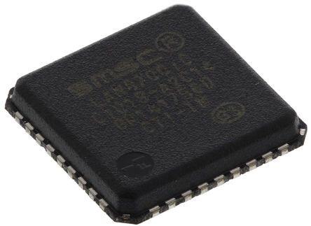
| 产品图片 |
|
| rohs | 符合RoHS无铅 / 符合限制有害物质指令(RoHS)规范要求 |
| 产品系列 | 通信及网络 IC,以太网 IC,Microchip Technology LAN8700iC-AEZG- |
| 数据手册 | |
| 产品型号 | LAN8700iC-AEZG |
| PCN组件/产地 | http://www.microchip.com/mymicrochip/NotificationDetails.aspx?id=5836&print=view |
| 产品 | Ethernet Transceivers |
| 产品目录页面 | |
| 产品种类 | 以太网 IC |
| 以太网连接类型 | 10 Base-T, 100 Base-TX |
| 供应商器件封装 | 36-QFN(6x6) |
| 其它名称 | 638-1047 |
| 包装 | 托盘 |
| 协议 | MII,RMII |
| 双工 | 全 |
| 商标 | Microchip Technology |
| 安装类型 | 表面贴装 |
| 安装风格 | SMD/SMT |
| 封装 | Tray |
| 封装/外壳 | 36-VFQFN 裸露焊盘 |
| 封装/箱体 | QFN-36 |
| 工作温度 | 0°C ~ 70°C |
| 工厂包装数量 | 4900 |
| 接收器滞后 | - |
| 支持标准 | 802.3, 802.3ab, MII |
| 收发器数量 | 1 Transceiver |
| 数据速率 | 10 Mb/s, 100 Mb/s |
| 最大工作温度 | + 70 C |
| 最大电源电流 | 39 mA, 81.6 mA |
| 最小工作温度 | 0 C |
| 标准包装 | 490 |
| 电压-电源 | 3 V ~ 3.6 V |
| 电源电压-最大 | 3.3 V |
| 电源电压-最小 | 1.8 V |
| 类型 | MII/RMII Ethernet Transceiver |
| 驱动器/接收器数 | - |


- 商务部:美国ITC正式对集成电路等产品启动337调查
- 曝三星4nm工艺存在良率问题 高通将骁龙8 Gen1或转产台积电
- 太阳诱电将投资9.5亿元在常州建新厂生产MLCC 预计2023年完工
- 英特尔发布欧洲新工厂建设计划 深化IDM 2.0 战略
- 台积电先进制程称霸业界 有大客户加持明年业绩稳了
- 达到5530亿美元!SIA预计今年全球半导体销售额将创下新高
- 英特尔拟将自动驾驶子公司Mobileye上市 估值或超500亿美元
- 三星加码芯片和SET,合并消费电子和移动部门,撤换高东真等 CEO
- 三星电子宣布重大人事变动 还合并消费电子和移动部门
- 海关总署:前11个月进口集成电路产品价值2.52万亿元 增长14.8%


PDF Datasheet 数据手册内容提取
LAN8700/LAN8700i ±15kV ESD Protected MII/RMII 10/100 Ethernet Transceiver with HP ® Auto-MDIX Support and flexPWR Technology in a Small Footprint PRODUCT FEATURES Data Brief (cid:132) Single-Chip Ethernet Physical Layer Transceiver (cid:132) Vendor Specific register functions (PHY) (cid:132) Low profile 36-pin QFN lead-free RoHS compliant (cid:132) ESD Protection levels of ±8kV HBM without external package (6 x 6 x 0.9mm height) protection devices (cid:132) 4 LED status indicators (cid:132) ESD protection levels of IEC61000-4-2, ±8kV contact (cid:132) Commercial Operating Temperature 0° C to 70° C mode, and ±15kV for air discharge mode per (cid:132) Industrial Operating Temperature -40° C to 85° C independent test facility version available (LAN8700i) (cid:132) Comprehensive flexPWR® Technology — Flexible Power Management Architecture Applications (cid:132) LVCMOS Variable I/O voltage range: +1.6V to +3.6V (cid:132) Integrated 3.3V to 1.8V regulator for optional single (cid:132) Set Top Boxes supply operation. — Regulator can be disabled if 1.8V system supply is (cid:132) Network Printers and Servers available. (cid:132) LAN on Motherboard (cid:132) Performs HP Auto-MDIX in accordance with IEEE (cid:132) 10/100 PCMCIA/CardBus Applications 802.3ab specification (cid:132) Embedded Telecom Applications (cid:132) Cable length greater than 150 meters (cid:132) Video Record/Playback Systems (cid:132) Automatic Polarity Correction (cid:132) Cable Modems/Routers (cid:132) Latch-Up Performance Exceeds 150mA per (cid:132) DSL Modems/Routers EIA/JESD 78, Class II (cid:132) Digital Video Recorders (cid:132) Energy Detect power-down mode (cid:132) Personal Video Recorders (cid:132) Low Current consumption power down mode (cid:132) IP and Video Phones (cid:132) Low operating current consumption: (cid:132) Wireless Access Points — 39mA typical in 10BASE-T and — 79mA typical in 100BASE-TX mode (cid:132) Digital Televisions (cid:132) Supports Auto-negotiation and Parallel Detection (cid:132) Digital Media Adaptors/Servers (cid:132) Supports the Media Independent Interface (MII) and (cid:132) POS Terminals Reduced Media Independent Interface (RMII) (cid:132) Automotive Networking (cid:132) Compliant with IEEE 802.3-2005 standards (cid:132) Gaming Consoles — MII Pins tolerant to 3.6V (cid:132) Security Systems (cid:132) IEEE 802.3-2005 compliant register functions (cid:132) POE Applications (cid:132) Integrated DSP with Adaptive Equalizer (cid:132) Access Control (cid:132) Baseline Wander (BLW) Correction PRODUCT PREVIEW SMSC LAN8700/LAN8700i Revision 2.3 (04-12-11)
±15kV ESD Protected MII/RMII 10/100 Ethernet Transceiver with HP Auto-MDIX Support and flexPWR® Technology in a Small Footprint Order Numbers: LAN8700C-AEZG for 36-pin, QFN lead-free RoHS compliant package LAN8700iC-AEZG for (Industrial Temp) 36-pin, QFN lead-free RoHS compliant package 4900 pcs per tray LAN8700C-AEZG-TR for 36-pin, QFN lead-free RoHS compliant package (tape and reel) 3000 pcs per reel This product meets the halogen maximum concentration values per IEC61249-2-21 For RoHS compliance and environmental information, please visit www.smsc.com/rohs 80 ARKAY DRIVE, HAUPPAUGE, NY 11788 (631) 435-6000 or 1 (800) 443-SEMI Copyright © 2011 SMSC or its subsidiaries. All rights reserved. Circuit diagrams and other information relating to SMSC products are included as a means of illustrating typical applications. Consequently, complete information sufficient for construction purposes is not necessarily given. Although the information has been checked and is believed to be accurate, no responsibility is assumed for inaccuracies. SMSC reserves the right to make changes to specifications and product descriptions at any time without notice. Contact your local SMSC sales office to obtain the latest specifications before placing your product order. The provision of this information does not convey to the purchaser of the described semiconductor devices any licenses under any patent rights or other intellectual property rights of SMSC or others. All sales are expressly conditional on your agreement to the terms and conditions of the most recently dated version of SMSC's standard Terms of Sale Agreement dated before the date of your order (the "Terms of Sale Agreement"). The product may contain design defects or errors known as anomalies which may cause the product's functions to deviate from published specifications. Anomaly sheets are available upon request. SMSC products are not designed, intended, authorized or warranted for use in any life support or other application where product failure could cause or contribute to personal injury or severe property damage. Any and all such uses without prior written approval of an Officer of SMSC and further testing and/or modification will be fully at the risk of the customer. Copies of this document or other SMSC literature, as well as the Terms of Sale Agreement, may be obtained by visiting SMSC’s website at http://www.smsc.com. SMSC is a registered trademark of Standard Microsystems Corporation (“SMSC”). Product names and company names are the trademarks of their respective holders. SMSC DISCLAIMS AND EXCLUDES ANY AND ALL WARRANTIES, INCLUDING WITHOUT LIMITATION ANY AND ALL IMPLIED WARRANTIES OF MERCHANTABILITY, FITNESS FOR A PARTICULAR PURPOSE, TITLE, AND AGAINST INFRINGEMENT AND THE LIKE, AND ANY AND ALL WARRANTIES ARISING FROM ANY COURSE OF DEALING OR USAGE OF TRADE. IN NO EVENT SHALL SMSC BE LIABLE FOR ANY DIRECT, INCIDENTAL, INDIRECT, SPECIAL, PUNITIVE, OR CONSEQUENTIAL DAMAGES; OR FOR LOST DATA, PROFITS, SAVINGS OR REVENUES OF ANY KIND; REGARDLESS OF THE FORM OF ACTION, WHETHER BASED ON CONTRACT; TORT; NEGLIGENCE OF SMSC OR OTHERS; STRICT LIABILITY; BREACH OF WARRANTY; OR OTHERWISE; WHETHER OR NOT ANY REMEDY OF BUYER IS HELD TO HAVE FAILED OF ITS ESSENTIAL PURPOSE, AND WHETHER OR NOT SMSC HAS BEEN ADVISED OF THE POSSIBILITY OF SUCH DAMAGES. Revision 2.3 (04-12-11) 2 SMSC LAN8700/LAN8700i PRODUCT PREVIEW
±15kV ESD Protected MII/RMII 10/100 Ethernet Transceiver with HP Auto-MDIX Support and flexPWR® Technology in a Small Footprint General Description The SMSC LAN8700/LAN8700i is a low-power, industrial temperature (LAN8700i), variable I/O voltage, analog interface IC with HP Auto-MDIX support for high-performance embedded Ethernet applications. The LAN8700/LAN8700i can be configured to operate on a single 3.3V supply utilizing an integrated 3.3V to 1.8V linear regulator. An option is available to disable the linear regulator to optimize system designs that have a 1.8V power plane available. 0.1 Architectural Overview The LAN8700/LAN8700i consists of an encoder/decoder, scrambler/descrambler, wave-shaping transmitter, output driver, twisted-pair receiver with adaptive equalizer and baseline wander (BLW) correction, and clock and data recovery functions. The LAN8700/LAN8700i can be configured to support either the Media Independent Interface (MII) or the Reduced Media Independent Interface (RMII). The LAN8700/LAN8700i is compliant with IEEE 802.3-2005 standards (MII Pins tolerant to 3.6V) and supports both IEEE 802.3-2005 compliant and vendor-specific register functions. It contains a full- duplex 10-BASE-T/100BASE-TX transceiver and supports 10-Mbps (10BASE-T) operation on Category 3 and Category 5 unshielded twisted-pair cable, and 100-Mbps (100BASE-TX) operation on Category 5 unshielded twisted-pair cable. 10/100 Media SMSC Magnetics Ethernet Access LAN8700/ System Bus Controller LAN8700i (MAC) MII /RMII LEDS/GPIO or SOC 25 MHz (MII) or 50MHz (RMIII) Crystal or External Clock Figure1 LAN8700/LAN8700i System Block Diagram Hubs and switches with multiple integrated MACs and external PHYs can have a large pin count due to the high number of pins needed for each MII interface. An increasing pin count causes increasing cost. The RMII interface is intended for use on Switch based ASICs or other embedded solutions requiring minimal pincount for ethernet connectivity. RMII requires only 6 pins for each MAC to PHY interface plus one common reference clock. The MII requires 16 pins for each MAC to PHY interface. The SMSC LAN8700/LAN8700i is capable of running in RMII mode. Please contact your SMSC sales representative for the latest RMII specification. The LAN8700/LAN8700i referenced throughout this document applies to both the commercial temperature and industrial temperature components. The LAN8700i refers to only the industrial temperature component. SMSC LAN8700/LAN8700i 3 Revision 2.3 (04-12-11) PRODUCT PREVIEW
±15kV ESD Protected MII/RMII 10/100 Ethernet Transceiver with HP Auto-MDIX Support and flexPWR® Technology in a Small Footprint MODE0 Auto- 10M Tx 10M HP Auto-MDIX MODE1 MODE Control MODE2 Negotiation Logic Transmitter TXP / TXN nRST SMI Management Transmit Section RXP / RXN Control 100M Tx 100M MII Logic Transmitter MDIX Control TXD[0..3] XTAL1 TX_EN 100M Rx DSP System: Analog-to- PLL TX_ER XTAL2 TX_CLK R Logic Clock Digital RXD[0..3] MII / M DaEtaq Ruaelcizoevrery GInetneerrruaptotr nINT RRXX__DERV II Lo Receive Section 100M PLL AdPdHreYss PHYAD[0..4] RX_CLK gic Latches 10M Rx Squelch & SPEED100 LINK CRS Logic Filters LED Circuitry ACTIVITY COL/CRS_DV FDUPLEX MDC MDIO 10M PLL Central Bias Figure2 LAN8700/LAN8700i Architectural Overview Revision 2.3 (04-12-11) 4 SMSC LAN8700/LAN8700i PRODUCT PREVIEW
±15kV ESD Protected MII/RMII 10/100 Ethernet Transceiver with HP Auto-MDIX Support and flexPWR® Technology in a Small Footprint Pin Diagram V D _ S R C RMII/ A3.3 ES1 A3.3 A3.3 L/ D R D P N D P N O D X D X X D X X C V E V R R V T T 6 5 4 3 2 1 0 9 8 3 3 3 3 3 3 3 2 2 nINT/TX_ER/TXD4 1 27 TXD3 MDC 2 26 TXD2 CRS/PHYAD4 3 25 VDDIO LAN8700/LAN8700i MDIO 4 24 TXD1 MII/RMII Ethernet PHY nRST 5 36 Pin QFN 23 TXD0 TX_EN 6 22 TX_CLK GND FLAG VDD33 7 21 RX_ER/RXD4 VDD_CORE 8 20 RX_CLK/REGOFF SPEED100/PHYAD0 9 19 RX_DV 0 1 2 3 4 5 6 7 8 1 1 1 1 1 1 1 1 1 1 2 3 2 L 2 1 0 D D D L 1 E E E E HYA HYA HYA XTA XTAL NTS MOD MOD MOD NK/P TY/P EX/P KIN/ D3/nI XD2/ XD1/ XD0/ LI TIVI UPL CL RX R R R C D A F Figure3 LAN8700/LAN8700i Package Pin Diagram (Top View) SMSC LAN8700/LAN8700i 5 Revision 2.3 (04-12-11) PRODUCT PREVIEW
±15kV ESD Protected MII/RMII 10/100 Ethernet Transceiver with HP Auto-MDIX Support and flexPWR® Technology in a Small Footprint Table1 LAN8700/LAN8700i 36-PIN QFN Pinout PIN NO. PIN NAME PIN NO. PIN NAME 1 nINT/TX_ER/TXD4 19 RX_DV 2 MDC 20 RX_CLK/REGOFF 3 CRS/PHYAD4 21 RX_ER/RXD4 4 MDIO 22 TXCLK 5 nRST 23 TXD0 6 TX_EN 24 TXD1 7 VDD33 25 VDDIO 8 VDD_CORE 26 TXD2 9 SPEED100/PHYAD0 27 TXD3 10 LINK/PHYAD1 28 TXN 11 ACTIVITY/PHYAD2 29 TXP 12 FDUPLEX/PHYAD3 30 VDDA3.3 13 XTAL2 31 RXN 14 CLKIN/XTAL1 32 RXP 15 RXD3/nINTSEL 33 VDDA3.3 16 RXD2/MODE2 34 EXRES1 17 RXD1/MODE1 35 VDDA3.3 18 RXD0/MODE0 36 COL/MII/CRS_DV Revision 2.3 (04-12-11) 6 SMSC LAN8700/LAN8700i PRODUCT PREVIEW
±15kV ESD Protected MII/RMII 10/100 Ethernet Transceiver with HP Auto-MDIX Support and flexPWR® Technology in a Small Footprint Pin Description This section describes the signals on each pin. When a lower case “n” is used at the beginning of the signal name, it indicates that the signal is active low. For example, nRST indicates that the reset signal is active low. I/O Signals I Input. Digital LVCMOS levels. O Output. Digital LVCMOS levels. I/O Input or Output. Digital LVCMOS levels. Note: The digital signals are not 5V tolerant.They are variable voltage from +1.6V to +3.6V. AI Input. Analog levels. AO Output. Analog levels. Table2 MII Signals SIGNAL NAME TYPE DESCRIPTION TXD0 I Transmit Data 0: Bit 0 of the 4 data bits that are accepted by the PHY for transmission. TXD1 I Transmit Data 1: Bit 1 of the 4 data bits that are accepted by the PHY for transmission. TXD2 I Transmit Data 2: Bit 2 of the 4 data bits that are accepted by the PHY for transmission Note: This signal should be grounded in RMII Mode. TXD3 I Transmit Data 3: Bit 3 of the 4 data bits that are accepted by the PHY for transmission. Note: This signal should be grounded in RMII Mode nINT/ I/O MII Transmit Error: When driven high, the 4B/5B encode TX_ER/ process substitutes the Transmit Error code-group (/H/) for the TXD4 encoded data word. This input is ignored in 10Base-T operation. MII Transmit Data 4: In Symbol Interface (5B Decoding) mode, this signal becomes the MII Transmit Data 4 line, the MSB of the 5-bit symbol code-group. Notes: (cid:132)This signal is not used in RMII Mode. (cid:132)This signal is mux’d with nINT TX_EN I Transmit Enable: Indicates that valid data is presented on the TXD[3:0] signals, for transmission. In RMII Mode, only TXD[1:0] have valid data. TX_CLK O Transmit Clock: 25MHz in 100Base-TX mode. 2.5MHz in 10Base-T mode. Note: This signal is not used in RMII Mode RXD0/ I/O Receive Data 0: Bit 0 of the 4 data bits that are sent by the PHY MODE0 in the receive path. PHY Operating Mode Bit 0: set the default MODE of the PHY. SMSC LAN8700/LAN8700i 7 Revision 2.3 (04-12-11) PRODUCT PREVIEW
±15kV ESD Protected MII/RMII 10/100 Ethernet Transceiver with HP Auto-MDIX Support and flexPWR® Technology in a Small Footprint Table2 MII Signals (continued) SIGNAL NAME TYPE DESCRIPTION RXD1/ I/O Receive Data 1: Bit 1 of the 4 data bits that are sent by the PHY MODE1 in the receive path. PHY Operating Mode Bit 1: set the default MODE of the PHY. RXD2/ I/O Receive Data 2: Bit 2 of the 4 data bits that are sent by the PHY MODE2 in the receive path. PHY Operating Mode Bit 2: set the default MODE of the PHY. Notes: (cid:132)RXD2 is not used in RMII Mode. RXD3/ I/O Receive Data 3: Bit 3 of the 4 data bits that are sent by the PHY nINTSEL in the receive path. nINTSEL: On power-up or external reset, the mode of the nINT/TXER/TXD4 pin is selected. (cid:132)When RXD3/nINTSEL is floated or pulled to VDDIO, nINT is selected for operation on pin nINT/TXER/TXD4 (default). (cid:132)When RXD3/nINTSEL is pulled low to VSS through a resistor, TXER/TXD4 is selected for operation on pin nINT/TXER/TXD4. Notes: (cid:132)RXD3 is not used in RMII Mode (cid:132)If the nINT/TXER/TXD4 pin is configured for nINT mode, then a pull-up resistor is needed to VDDIO on the nINT/TXER/TXD4 pin. RX_ER/ O Receive Error: Asserted to indicate that an error was detected RXD4/ somewhere in the frame presently being transferred from the PHY. MII Receive Data 4: In Symbol Interface (5B Decoding) mode, this signal is the MII Receive Data 4 signal, the MSB of the received 5-bit symbol code-group. Unless configured in this mode, the pin functions as RX_ER. Note: This pin has an internal pull-down resistor, and must not be high during reset. The RX_ER signal is optional in RMII Mode. RX_DV O Receive Data Valid: Indicates that recovered and decoded data nibbles are being presented on RXD[3:0]. Note: This pin has an internal pull-down resistor, and must not be high during reset. This signal is not used in RMII Mode. RX_CLK/ I/O Receive Clock: In MII mode, this pin is the receive clock output. REGOFF 25MHz in 100Base-TX mode. 2.5MHz in 10Base-T mode. Note: This signal is not used in RMII Mode. Regulator Off: This pin may be used to configure the internal 1.8V regulator off. This pin is sampled during the power-on sequence to determine if the internal regulator should turn on. When the regulator is disabled, external 1.8V must be supplied to VDD_CORE, and the voltage at VDD33 must be at least 2.64V before voltage is applied to VDD_CORE. Revision 2.3 (04-12-11) 8 SMSC LAN8700/LAN8700i PRODUCT PREVIEW
±15kV ESD Protected MII/RMII 10/100 Ethernet Transceiver with HP Auto-MDIX Support and flexPWR® Technology in a Small Footprint Table2 MII Signals (continued) SIGNAL NAME TYPE DESCRIPTION COL/ I/O MII Mode Collision Detect: Asserted to indicate detection of RMII/ collision condition. CRS_DV RMII – MII/RMII mode selection is latched on the rising edge of the internal reset (nreset) based on the following strapping: (cid:132)Float this pin for MII mode or pull-high with an external resistor to VDDIO to set the device in RMII mode. RMII Mode CRS_DV (Carrier Sense/Receive Data Valid) Asserted to indicate when the receive medium is non-idle. When a 10BT packet is received, CRS_DV is asserted, but RXD[1:0] is held low until the SFD byte (10101011) is received. In 10BT, half- duplex mode, transmitted data is not looped back onto the receive data pins, per the RMII standard. CRS/ I/O Carrier Sense: Indicates detection of carrier. PHYAD4 Note: This signal is mux’d with PHYAD4 Table3 LED Signals SIGNAL NAME TYPE DESCRIPTION SPEED100/ I/O LED1 – SPEED100 indication. Active indicates that the selected PHYAD0 speed is 100Mbps. Inactive indicates that the selected speed is 10Mbps. Note: This signal is mux’d with PHYAD0 LINK/ I/O LED2 – LINK ON indication. Active indicates that the Link PHYAD1 (100Base-TX or 10Base-T) is on. Note: This signal is mux’d with PHYAD1 ACTIVITY/ I/O LED3 – ACTIVITY indication. Active indicates that there is PHYAD2 Carrier sense (CRS) from the active PMD. Note: This signal is mux’d with PHYAD2 FDUPLEX/ I/O LED4 – DUPLEX indication. Active indicates that the PHY is in PHYAD3 full-duplex mode. Note: This signal is mux’d with PHYAD3 Table4 Management Signals SIGNAL NAME TYPE DESCRIPTION MDIO I/O Management Data Input/OUTPUT: Serial management data input/output. MDC I Management Clock: Serial management clock. SMSC LAN8700/LAN8700i 9 Revision 2.3 (04-12-11) PRODUCT PREVIEW
±15kV ESD Protected MII/RMII 10/100 Ethernet Transceiver with HP Auto-MDIX Support and flexPWR® Technology in a Small Footprint Table5 Boot Strap Configuration Inputs(Note1) SIGNAL NAME TYPE DESCRIPTION CRS/ I/O PHY Address Bit 4: set the default address of the PHY. This PHYAD4 signal is mux’d with CRS Note: This signal is mux’d with CRS FDUPLEX/ I/O PHY Address Bit 3: set the default address of the PHY. PHYAD3 Note: This signal is mux’d with FDUPLEX ACTIVITY/ I/O PHY Address Bit 2: set the default address of the PHY. PHYAD2 Note: This signal is mux’d with ACTIVITY LINK/ I/O PHY Address Bit 1: set the default address of the PHY. PHYAD1 Note: This signal is mux’d with LINK SPEED100/ I/O PHY Address Bit 0: set the default address of the PHY. PHYAD0 Note: This signal is mux’d with SPEED100 RXD2/ I/O PHY Operating Mode Bit 2: set the default MODE of the PHY. MODE2 Note: This signal is mux’d with RXD2 RXD1/ I/O PHY Operating Mode Bit 1: set the default MODE of the PHY. MODE1 Note: This signal is mux’d with RXD1 RXD0/ I/O PHY Operating Mode Bit 0: set the default MODE of the PHY. MODE0 Note: This signal is mux’d with RXD0 RX_CLK/ I/O Internal Regulator off: disable the internal +1.8v regulator. REGOFF This signal is mux’d with RX_CLK. (cid:132)Float to enable the internal +1.8v regulator. (cid:132)Pull up with a resistor to VDDIO to disable the internal regulator. COL/ I/O Digital Communication Mode: set the digital communications RMII/ mode of the PHY to RMII or MII. This signal is muxed with the CRS_DV Collision signal (MII mode) and Carrier Sense/ receive Data Valid (RMII mode) (cid:132)Float for MII mode. (cid:132)Pull up with a resistor to VDDIO for RMII mode. RXD3/ I/O nINT pin mode select: set the mode of pin 1. nINTSEL (cid:132)Default, left floating pin 1 is nINT, active low interrupt output. Note: For nINT mode, tie nINT/TXD4/TXER to VDDIO with a resistor. (cid:132)Pulled to VSS by a resistor, pin 1 is TX_ER/TXD4, Transmit Error or Transmit data 4 (5B mode). Note: For TXD4/TXER mode, do not tie nINT/TXD4/TXER to VDDIO or Ground. Note1 On nRST transition high, the PHY latches the state of the configuration pins in this table. Revision 2.3 (04-12-11) 10 SMSC LAN8700/LAN8700i PRODUCT PREVIEW
±15kV ESD Protected MII/RMII 10/100 Ethernet Transceiver with HP Auto-MDIX Support and flexPWR® Technology in a Small Footprint Table6 General Signals SIGNAL NAME TYPE DESCRIPTION nINT/ I/O LAN Interrupt – Active Low output. Place an external resistor TX_ER/ pull-up to VCC 3.3V. TXD4 Note: This signal is mux’d with TXER/TXD4 nRST I External Reset – input of the system reset. This signal is active LOW. CLKIN/ I/O Clock Input – 25 Mhz or 50 MHz external clock or crystal input. XTAL1 In MII mode, this signal is the 25 MHz reference input clock In RMII mode, this signal is the 50 MHz reference input clock which is typically also driven to the RMII compliant Ethernet MAC clock input. XTAL2 O Clock Output – 25 MHz crystal output. Note: Float this pin if using an external clock being driven through CLKIN/XTAL1 Table7 10/100 Line Interface SIGNAL NAME TYPE DESCRIPTION TXP AO Transmit Data Positive: 100Base-TX or 10Base-T differential transmit outputs to magnetics. TXN AO Transmit Data Negative: 100Base-TX or 10Base-T differential transmit outputs to magnetics. RXP AI Receive Data Positive: 100Base-TX or 10Base-T differential receive inputs from magnetics. RXN AI Receive Data Negative: 100Base-TX or 10Base-T differential receive inputs from magnetics. Table8 Analog References SIGNAL NAME TYPE DESCRIPTION EXRES1 AI Connects to reference resistor of value 12.4K-Ohm, 1% connected as described in the Analog Layout Guidelines. Table9 Power Signals SIGNAL NAME TYPE DESCRIPTION VDDIO POWER +1.6V to +3.6V Variable I/O Pad Power VDD33 POWER +3.3V Core Regulator Input. VDDA3.3 POWER +3.3V Analog Power SMSC LAN8700/LAN8700i 11 Revision 2.3 (04-12-11) PRODUCT PREVIEW
±15kV ESD Protected MII/RMII 10/100 Ethernet Transceiver with HP Auto-MDIX Support and flexPWR® Technology in a Small Footprint Table9 Power Signals (continued) SIGNAL NAME TYPE DESCRIPTION VDD_CORE POWER +1.8V (Core voltage) - 1.8V for digital circuitry on chip. Supplied by the on-chip regulator unless configured for regulator off mode using the RX_CLK/REGOFF pin. Place a 0.1uF capacitor near this pin and connect the capacitor from this pin to ground. When using the on-chip regulator, place a 4.7uF ±20% capacitor with ESR < 1ohm near this pin and connect the capacitor from this pin to ground. X5R or X7R ceramic capacitors are recommended since they exhibit an ESR lower than 0.1ohm at frequencies greater than 10kHz. Exposed Ground Flag. The flag must be connected to the ground plane with an array of vias as described in the Analog VSS POWER Layout Guidelines Revision 2.3 (04-12-11) 12 SMSC LAN8700/LAN8700i PRODUCT PREVIEW
±15kV ESD Protected MII/RMII 10/100 Ethernet Transceiver with HP Auto-MDIX Support and flexPWR® Technology in a Small Footprint Package Outline Figure4 36-Pin QFN Package Outline, 6 x 6 x 0.90 mm Body (Lead-Free) Table10 36-Pin QFN Package Parameters MIN NOMINAL MAX REMARKS A 0.80 ~ 1.00 Overall Package Height A1 0 ~ 0.05 Standoff A2 0.60 ~ 0.80 Mold Thickness A3 0.20 REF Copper Lead-frame Substrate D 5.85 ~ 6.15 X Overall Size D1 5.55 ~ 5.95 X Mold Cap Size D2 3.55 ~ 3.85 X exposed Pad Size E 5.85 ~ 6.15 Y Overall Size E1 5.55 ~ 5.95 Y Mold Cap Size E2 3.55 ~ 3.85 Y exposed Pad Size L 0.35 ~ 0.75 Terminal Length e 0.50 Basic Terminal Pitch b 0.18 ~ 0.30 Terminal Width ccc ~ ~ 0.08 Coplanarity Notes: 1. Controlling Unit: millimeter. 2. Dimension b applies to plated terminals and is measured between 0.15mm and 0.30mm from the terminal tip. Tolerance on the true position of the terminal is ± 0.05 mm at maximum material conditions (MMC). 3. Details of terminal #1 identifier are optional but must be located within the zone indicated. 4. Coplanarity zone applies to exposed pad and terminals. SMSC LAN8700/LAN8700i 13 Revision 2.3 (04-12-11) PRODUCT PREVIEW
Mouser Electronics Authorized Distributor Click to View Pricing, Inventory, Delivery & Lifecycle Information: M icrochip: LAN8700C-AEZG-TR LAN8700IC-AEZG-TR LAN8700C-AEZG LAN8700iC-AEZG