ICGOO在线商城 > 集成电路(IC) > PMIC - 稳压器 - DC DC 开关稳压器 > L4972A
 Datasheet下载
- 型号: L4972A
- 制造商: STMicroelectronics
- 库位|库存: xxxx|xxxx
- 要求:
| 数量阶梯 | 香港交货 | 国内含税 |
| +xxxx | $xxxx | ¥xxxx |
查看当月历史价格
查看今年历史价格
L4972A产品简介:
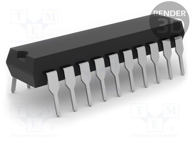
ICGOO电子元器件商城为您提供L4972A由STMicroelectronics设计生产,在icgoo商城现货销售,并且可以通过原厂、代理商等渠道进行代购。 L4972A价格参考¥21.26-¥51.72。STMicroelectronicsL4972A封装/规格:PMIC - 稳压器 - DC DC 开关稳压器, 可调式 降压 开关稳压器 IC 正 5.1V 1 输出 2A 20-DIP(0.300",7.62mm)。您可以下载L4972A参考资料、Datasheet数据手册功能说明书,资料中有L4972A 详细功能的应用电路图电压和使用方法及教程。
STMicroelectronics 的 L4972A 是一款单片集成的 DC-DC 降压型开关稳压器,广泛应用于需要高效、中等功率电源转换的场景。其典型应用场景包括:

1. 工业控制系统:如PLC、传感器供电、工业自动化设备中的电源模块,提供稳定电压输出。

2. 汽车电子:车载电子系统如ECU、导航系统、车载娱乐系统中,用于将汽车电瓶电压(如12V)转换为芯片所需的5V或更低电压。

3. 通信设备:用于路由器、交换机、基站设备中的辅助电源系统,提供高效、可靠的电压调节。

4. 消费电子产品:如打印机、扫描仪、数码相机等设备中的电源管理模块。

5. 医疗设备:便携式或固定式医疗仪器中,用于为微处理器、传感器等提供稳定电源。

L4972A 具有宽输入电压范围(8V至40V)、内置功率MOSFET、过热与过流保护功能,适合中高功率应用,且外围电路简洁,适用于对可靠性与效率要求较高的场合。
| 参数 | 数值 |
| 产品目录 | 集成电路 (IC)半导体 |
| 描述 | IC REG BUCK ADJ 2A 20DIP稳压器—开关式稳压器 5.1 to 40V 2.0 Amp |
| 产品分类 | |
| 品牌 | STMicroelectronics |
| 产品手册 | |
| 产品图片 |
|
| rohs | 符合RoHS无铅 / 符合限制有害物质指令(RoHS)规范要求 |
| 产品系列 | 电源管理 IC,稳压器—开关式稳压器,STMicroelectronics L4972A- |
| 数据手册 | |
| 产品型号 | L4972A |
| PWM类型 | - |
| 产品培训模块 | http://www.digikey.cn/PTM/IndividualPTM.page?site=cn&lang=zhs&ptm=26258 |
| 产品目录页面 | |
| 产品种类 | 稳压器—开关式稳压器 |
| 供应商器件封装 | 20-PowerDIP |
| 关闭 | Shutdown |
| 其它名称 | 497-6698-5 |
| 其它有关文件 | http://www.st.com/web/catalog/sense_power/FM142/CL1456/SC355/PF75165?referrer=70071840 |
| 包装 | 管件 |
| 同步整流器 | 无 |
| 商标 | STMicroelectronics |
| 安装类型 | 通孔 |
| 安装风格 | Through Hole |
| 宽度 | 7.1 mm |
| 封装 | Tube |
| 封装/外壳 | 20-DIP(0.300",7.62mm) |
| 封装/箱体 | PDIP-20 |
| 工作温度 | -40°C ~ 150°C |
| 工作温度范围 | - 40 C to + 150 C |
| 工厂包装数量 | 20 |
| 开关频率 | 200 kHz |
| 拓扑结构 | Buck |
| 最大工作温度 | + 150 C |
| 最大输入电压 | 55 V |
| 最小工作温度 | - 40 C |
| 最小输入电压 | 15 V |
| 标准包装 | 20 |
| 电压-输入 | 15 V ~ 50 V |
| 电压-输出 | 5.1 V ~ 40 V |
| 电流-输出 | 2A |
| 电源电压-最小 | 15 V |
| 电源电流 | 16 mA |
| 类型 | Step-Down |
| 系列 | L4972 |
| 输入电压 | 15 V to 50 V |
| 输出数 | 1 |
| 输出电压 | 50 V |
| 输出电流 | 2 A |
| 输出端数量 | 1 Output |
| 输出类型 | 可调式 |
| 频率-开关 | 100kHz |

(NARROW%20PDIP%20MDIP)%20SERIES.JPG)


- 商务部:美国ITC正式对集成电路等产品启动337调查
- 曝三星4nm工艺存在良率问题 高通将骁龙8 Gen1或转产台积电
- 太阳诱电将投资9.5亿元在常州建新厂生产MLCC 预计2023年完工
- 英特尔发布欧洲新工厂建设计划 深化IDM 2.0 战略
- 台积电先进制程称霸业界 有大客户加持明年业绩稳了
- 达到5530亿美元!SIA预计今年全球半导体销售额将创下新高
- 英特尔拟将自动驾驶子公司Mobileye上市 估值或超500亿美元
- 三星加码芯片和SET,合并消费电子和移动部门,撤换高东真等 CEO
- 三星电子宣布重大人事变动 还合并消费电子和移动部门
- 海关总署:前11个月进口集成电路产品价值2.52万亿元 增长14.8%


PDF Datasheet 数据手册内容提取
L4972A 2A SWITCHING REGULATOR 1 Features Figure 1. Packages ■ 2A OUTPUT CURRENT ■ 5.1V TO 40V OUTPUT VOLTAGE RANGE ■ 0 TO 90% DUTY CYCLE RANGE ■ INTERNAL FEED-FORWARD LINE REG. PowerDIP20 (16+2+2) SO20 ■ INTERNAL CURRENT LIMITING ■ PRECISE 5.1V ± 2% ON CHIP REFERENCE Table 1. Order Codes ■ RESET AND POWER FAIL FUNCTIONS Part Number Package ■ INPUT/OUTPUT SYNC PIN L4972A DIP20 (16+2+20) ■ UNDER VOLTAGE LOCK OUT WITH HYSTERETIC TURN-ON L4972AD SO20 ■ PWM LATCH FOR SINGLE PULSE PER L4972AD013TR SO20 in Tape & Reel PERIOD ■ VERY HIGH EFFICIENCY uses a DMOS output transistor to obtain very high ■ SWITCHING FREQUENCY UP TO 200KHz efficiency and very fast switching times. Features ■ THERMAL SHUTDOWN of the L4972 include reset and power fail for micro- ■ CONTINUOUS MODE OPERATION processors, feed forward line regulation, soft start, limiting current and thermal protection. The device 2 Description is mounted in a Powerdip 16 + 2 + 2 and SO20 large plastic packages and requires few external The L4972A is a stepdown monolithic power components. Efficient operation at switching fre- switching regulator delivering 2A at a voltage vari- quencies up to 200KHz allows reduction in the able from 5.1 to 40V. size and cost of external filter component. Realized with BCD mixed technology, the device Figure 2. Block Diagram Rev. 3 May 2005 1/22
L4972A Table 2. Pin Description N° Pin Function 1 BOOTSTRAP A Cboot capacitor connected between this terminal and the output allows to drive properly the internal D-MOS transistor. 2 RESET DELAY A Cd capacitor connected between this terminal and ground determines the reset signal delay time. 3 RESET OUT Open Collector Reset/power Failand the output voltages are safe. Signal Output. This output is high when the supply 4 RESET INPUT Input of Power Fail Circuit. The threshold is 5.1V. It may be connected via a divider to the input for power fail function. It must be connected to the pin 14 an external 30KΩ resistor when power fail signal not required. 5, 6 15, GROUND Common Ground Terminal 16 7 FREQUENCY A series RC network connected between this terminal and ground determines the COMPENSATION regulation loop gain characteristics. 8 SOFT START Soft Start Time Constant. A capacitor is connected between the sterminal and ground to define the soft start time constant. 9 FEEDBACK INPUT The Feedback Terminal of the Regulation Loop. The output is connected directly to this terminal for 5.1V operation; It is connected via a divider for higher voltages. 10 SYNC INPUT Multiple L4972A’s are synchronized by connecting pin 10 inputs together or via an external syncr. pulse. 11 SUPPLY VOLTAGE Unregulated Input Voltage. 12, 19 N.C. Not Connected. 13 Vref 5.1V Vref Device Reference Voltage. 14 Vstart Internal Start-up Circuit to Drive the Power Stage. 17 OSCILLATOR Rosc. External resistor connected to ground determines the constant charging current of Cosc. 18 OSCILLATOR Cosc. External capacitor connected to ground determines (with Rosc) the switching frequency. 20 OUTPUT Regulator Output. Figure 3. Pin Connection (Top view) BOOTSTRAP 1 20 OUTPUT RESET DELAY 2 19 N.C. RESET OUT 3 18 C OSC P. FAIL INPUT 4 17 R OSC GND 5 16 GND GND 6 15 GND FREQ. COMP. 7 14 Vstart SOFT START 8 13 Vref FEEDBACK IN. 9 12 N.C. SYNC INPUT 10 11 Vi DIP20 2/22
L4972A Table 3. Absolute Maximum Ratings Symbol Parameter Value Unit V11 Input Voltage 55 V V11 Input Operating Voltage 50 V V20 Output DC Voltage -1 V Output Peak Voltage at t = 0.1µs f = 200kHz -5 V I20 Maximum Output Current Internally Limited VI Boostrap Voltage 65 V Boostrap Operating Voltage V11 + 15 V V4, V8 Input Voltage at Pins 4, 12 12 V V3 Reset Output Voltage 50 V I3 Reset Output Sink Current 50 mA V2, V7, V9, Input Voltage at Pin 2, 7, 9, 10 7 V V10 I2 Reset Delay Sink Current 30 mA I7 Error Amplifier Output Sink Current 1 A I8 Soft Start Sink Current 30 mA Ptot Total Power Dissipation at TPINS ≤ 90°C 5 / 3.75(*) W at Tamb = 70°C (No copper area on PCB) 1.3/1 (*) W TJ, Tstg Junction and Storage Temperature -40 to 150 °C (*) SO-20 Table 4. Thermal Data Symbol Parameter PowerDIP SO20 Unit Rth j-pins Thermal Resistance Junction-Pins max, 12 16 °C/W Rth j-amb Thermal Resistance Junction-ambient max, 60 80 °C/W 3 Circuit Operation The L4972A is a 2A monolithic stepdown switching regulator working in continuous mode realized in the new BCD Technology. This technology allows the integration of isolated vertical DMOS power transistors plus mixed CMOS/Bipolar transistors. The device can deliver 2A at an output voltage adjustable from 5.1V to 40V and contains diagnostic and control functions that make it particularly suitable for microprocessor based systems. 3.1 BLOCK DIAGRAM The block diagram shows the DMOS power transistors and the PWM control loop. Integrated functions include a reference voltage trimmed to 5.1V ± 2%, soft start, undervoltage lockout, oscillator with feedfor- ward control, pulse by pulse current limit, thermal shutdown and finally the reset and power fail circuit. The reset and power fail circuit provides an output signal for a microprocessor indicating the status of the sys- tem. Device turn on is around 11V with a typical 1V hysterysis, this threshold porvides a correct voltage for the driving stage of the DMOS gate and the hysterysis prevents instabilities. An external bootstrap capacitor charge to 12V by an internal voltage reference is needed to provide cor- rect gate drive to the power DMOS. The driving circuit is able to source and sink peak currents of around 0.5A to the gate of the DMOS transistor. A typical switching time of the current in the DMOS transistor is 50ns. Due to the fast commutation switching frequencies up to 200kHz are possible. The PWM control loop consists of a sawtooth oscillator, error amplifier, comparator, latch and the output 3/22
L4972A stage. An error signal is produced by comparing the output voltage with the precise 5.1V ± 2% on chip reference. This error signal is then compared with the sawtooth oscillator in order to generate frixed fre- quency pulse width modulated drive for the output stage. A PWM latch is included to eliminate multiple pulsing within a period even in noisy environments. The gain and stability of the loop can be adjusted by an external RC network connected to the output of the error amplifier. A voltage feedforward control has been added to the oscillator, this maintains superior line regulation over a wide input voltage range. Closing the loop directly gives an output vol-tage of 5.1V, higher voltages are obtained by inserting a voltage divider. At turn on, output overcurrents are prevented by the soft start function (fig. 5). The error amplifier is initially clamped by an external capacitor, Css, and allowed to rise linearly under the charge of an internal constant current source. Output overload protection is provided by a current limit circuit. The load current is sensed by a internal metal resistor connected to a comparator. When the load current exceeds a preset threshold, the output of the comparator sets a flip flop which turns off the power DMOS. The next clock pulse, from an internal 40kHz oscillator, will reset the flip flop and the power DMOS will again conduct. This current protection method, ensures a constant current output when the system is overloaded or short circuited and limits the switching frequency, in this condition, to 40kHz. The Reset and Power fail diagram (fig. 7), generates an output signal when the supply voltage exceeds a threshold programmed by an external voltage divider. The reset signal, is generated with a delay time programmed by a external capacitor on the delay pin. When the supply voltage falls below the threshold or the output voltage goes below 5V, the reset output goes low immediately. The reset output is an open drain. Fig. 7A shows the case when the supply voltage is higher than the threshold, but the output voltage is not yet 5V. Fig. 7B shows the case when the output is 5.1V, but the supply voltage is not yet higher than the fixed threshold. The thermal protection disables circuit operation when the junction temperature reaches about 150°C and has a hysterysis to prevent unstable conditions. Figure 4. Feedforward Waveform. Figure 5. Soft Start Function. 4/22
L4972A Figure 6. Limiting Current Function. Figure 7. Reset and Power Fail Functions A B 5/22
L4972A 4 Electrical Characteristcs Table 5. Electrical Characteristcs Refer to the test circuit, TJ = 25°C, Vi = 35V, R4 = 30KΩ, C9 = 2.7nF, fSW = 100KHz typ, unless otherwise specified. Symbol Parameter Test Condition Min. Typ. Max. Unit Fig. DYNAMIC CHARACTERISTICS Vi Input Volt. Range (pin 11) Vo = Vref to 40V Io = 2A (**) 15 50 V 8 Vo Output Voltage Vi =15V to 50V Io= 1A; 5 5.1 5.2 V 8 Vo = Vref ∆Vo Line Regulation Vi =15V to 50V 12 30 mV Io = 0.5A; Vo= Vref ∆Vo Load Regulation Vo = Vref Io= 0.5A to 2A 7 20 mV Vd Dropout Voltage between Pin Io = 2A 0.25 0.4 V 11 and 20 I20L Max Limiting Current Vi = 15V to 50V 2.5 2.8 3.5 A Vo= Vref to 40V η Efficiency (*) Io = 2A, f = 100KHz Vo = Vref 75 85 % Vo = 12V 90 % SVR Supply Voltage Ripple Rejection Vi = 2VRMS; Io= 1A 56 60 dB 8 f = 100Hz; Vo= Vref f Switching Frequency 90 100 110 KHz 8 ∆f/∆Vi Voltage Stability of Switching Vi = 15V to 45V 2 6 % 8 Frequency ∆f/Tj Temperature Stability of Tj = 0 to 125°C 1 % 8 Switching Frequency fmax Maximum Operating Switching Vo= Vref R4 = 15KΩ 200 KHz 8 Frequency Io = 2A C9= 2.2nF (*) Only for DIP version (**) Pulse testing with a low duty cycle Vref SECTION (pin 13) V13 Reference Voltage 5 5.1 5.2 V 10 ∆V13 Line Regulation Vi = 15V to 50V 10 25 mV 10 ∆V13 Load Regulation I13 = 0 to 1mA 20 40 mV 10 ∆V13 /∆T Average Temperature Tj = 0°C to 125°C 0.4 mV/°C 10 Coefficient Reference Voltage I13 short Short Circuit Current Limit V13 = 0 70 mA 10 VSTART SECTION (pin 15) V14 Reference Voltage 11.4 12 12.6 V 10 ∆V14 Line Regulation Vi = 15 to 50V 0.6 1.4 V 10 ∆V14 Load Regulation I14 = 0 to 1mA 50 200 mV 10 I14 short Short Circuit Current Limit V15 = 0V 80 mA 10 DC CHARACTERISTICS V11on Turn-on Threshold 10 11 12 V 12 V11 Hyst Turn-off Hysteresys 1 V 12 I11Q Quiescent Current V8 = 0; S1 = D 13 19 mA 12 I11OQ Operating Supply Current V8 = 0; S1 = B; S2 = B 16 23 mA 12 6/22
L4972A Table 5. Electrical Characteristcs (continued) Refer to the test circuit, TJ = 25°C, Vi = 35V, R4 = 30KΩ, C9 = 2.7nF, fSW = 100KHz typ, unless otherwise specified. Symbol Parameter Test Condition Min. Typ. Max. Unit Fig. I20L Out Leak Current Vi = 55V; S3 = A; V8= 0 2 mA 12 SOFT START (pin 8) I8 Soft Start Source Current V8 = 3V; V9= 0V 80 115 150 µA 13 V8 Output Saturation Voltage I8 = 20mA; V11= 10V 1 V 13 I8= 200µA; V11= 10V 0.7 V 13 ERROR AMPLIFIER V7H High Level Out Voltage I7 = 100µA; S1 = C; V9 = 4.7V 6 V 14 V7L Low Level Out Voltage I7 = 100µA; S1 = C; V9= 5.3V 1.2 V 14 I7H Source Output Current V7 = 1V; V7 = 4.7V 100 150 µA 14 -I7L Sink Output Current V7 = 6V; V9 = 5.3V 100 150 µA 14 I9 Input Bias Current S1 = B; RS = 10KΩ 0.4 3 µA 14 GV DC Open Loop Gain S1 = A; RS= 10Ω 60 dB 14 SVR Supply Voltage Rejection 15 < Vi < 50V 60 80 dB 14 VOS Input Offset Voltage RS= 50Ω S1 = A 2 10 mV 14 RAMP GENERATOR (pin 18) V18 Ramp Valley S1 = B; S2 = B 1.2 1.5 V 12 V18 Ramp Peak S1 = B; S2 = B Vi = 15V 2.5 V 12 Vi = 45V 5.5 V 12 I18 Min. Ramp Current S1 = A; I17= 100µA 270 300 µA 12 I18 Max. Ramp Current S1 = A; I17= 1mA 2.4 2.7 mA 12 SYNC FUNCTION (pin 10) V10 Low Input Voltage Vi = 15V to 50V; V8 = 0; –0.3 0.9 V 12 S1 = B; S2 = B; S4 = B V10 High Input voltage V8 = 0; S1 = B; S2 = B; S4 = B 2.5 5.5 V 12 I10L Sync Input Current with Low V10= V18= 0.9V; S4 = B; 0.4 mA 12 Input Voltage S1 = B; S2 = B I10H Input Current with High V10= 2.5V 1.5 mA 12 Input Voltage V10 Output Amplitude 4 5 V – tW Output Pulse Width Vthr = 2.5V 0.3 0.5 0.8 µs – RESET AND POWER FAIL FUNCTIONS V9R Rising Thereshold Voltage (pin 9) Vi = 15 to 50V Vref Vref Vref V 15 V4 = 5.3V -130 -100 -80 mV V9F Falling Thereshold Voltage (pin 9) Vi = 15 to 50V 4.77 Vref Vref V 15 V4 = 5.3V -200 -160 mV V2H Delay High Threshold Volt. Vi = 15 to 50V 4.95 5.1 5.25 V 15 V4 = 5.3V; V9 = V13 V2L Delay Low Threshold Volt. Vi = 15 to 50V;V4 = 4.7V; V9 = V13 1 1.1 1.2 V 15 I2SO Delay Source Current V4 = 5.3V; V2 = 3V 30 60 80 µA 15 I2SI Delay Source Sink Current V4 = 4.7V; V2 = 3V 10 mA 15 V3S Output Saturation Voltage I3 = 15mA; S1 = B V4 = 4.7V 0.4 V 15 I3 Output Leak Current V3 = 50V; S1 = A 100 µA 15 7/22
L4972A Table 5. Electrical Characteristcs (continued) Refer to the test circuit, TJ = 25°C, Vi = 35V, R4 = 30KΩ, C9 = 2.7nF, fSW = 100KHz typ, unless otherwise specified. Symbol Parameter Test Condition Min. Typ. Max. Unit Fig. V4R Rising Threshold Voltage V9 = V13 4.95 5.1 5.25 V 15 V4H Hysteresis 0.4 0.5 0.6 V 15 I4 Input Bias Current 1 3 µA 15 Figure 8. TYPICAL PERFORMANCES (using evaluation board) : n = 83% (V = 35V ; V = V ; I = 2A ; f = 100KHz) i o REF o sw V = 30mV (at 1A) o RIPPLE Line regulation = 12mV (V = 15 to 50V) i Load regulation = 7mV (I = 0.5 to 2A) o for component values Refer to the fig. 8 (Part list). Figure 9. Component Layout of fig. 8. Evaluation Board Available (only for DIP version) 8/22
L4972A PART LIST R1 = 30KΩ R2 = 10KΩ R3 = 15KΩ R4 = 30KΩ R5 = 22Ω R6 = 4.7KΩ R7 = see table 6 R8 = OPTION R9 = 4.7KΩ * C1 = C2 = 1000mF 63V EYF (ROE) C3 = C4 = C5 = C6 = 2,2µF 50V C7 = 390pF Film C8 = 22nF MKT 1837 (ERO) C9 = 2.7nF KP 1830 (ERO) C10 = 0.33µF Film C11 = 1nF ** C12 = C13 = C14 = 100µF 40V EKR (ROE) C15 = 1µF Film D1 = STPS5L60 L1 = 150µH core 58310 MAGNETICS 45 TURNS 0.91mm (AWG 19) COGEMA 949181 * 2 capacitors in parallel to increase input RMS current capability. * * 3 capacitors in parallel to reduce total output ESR. Table 6. V0 R9 R7 12V 4.7kΩ 6.2kΩ 15V 4.7kΩ 9.1kΩ 18V 4.7kΩ 12Ω 24V 4.7kΩ 18Ω Note: In the Test and Application Circuit for L4972D are not mounted C2, C14 and R8. Table 7. Suggested Boostrap Capacitors Operating Frequency Boostrap Cap.c10 f = 20KHz ≥680nF f = 50KHz ≥470nF f = 100KHz ≥330nF f = 200KHz ≥220nF f = 500KHz ≥100nF 9/22
L4972A Figure 10. P.C. Board and Component Layout of the Circuit of Fig. 8. Figure 11. DC Test Circuits Figure 12. 10/22
L4972A Figure 13. Figure 14. Figure 15. Figure 16. Quiescent Drain Current vs. Supply Figure 17. Quiescent Drain Current vs. Voltage (0% duty cycle - see fig. 12). Junction Temperature (0% duty cycle). 11/22
L4972A Figure 18. Quiescent Drain Current vs. Duty Figure 21. Reference Voltage (pin 14) vs. Vi Cycle. (see fig. 11). Figure 19. Reference Voltage (pin 13) vs. Vi Figure 22. Reference Voltage (pin 14) vs. (see fig. 11). Junction Temperature (see fig. 11). Figure 20. Reference Voltage (pin 13) vs. Figure 23. : Ref. Voltage 5.1V (pin 13) Supply Junction Temperature (see fig. 11). Voltage Ripple Rejection vs. Frequency 12/22
L4972A Figure 24. Switching Frequency vs. Input Figure 27. Maximum Duty Cycle vs. Frequency. Voltage (see fig. 8). Figure 25. Switching Frequency vs. Junction Figure 28. Supply Voltage Ripple Rejection vs. Temperature (see fig. 8). Frequency (see fig. 8). Figure 26. Switching Frequency vs. R4 (see Figure 29. Efficiency vs. Output Voltage. fig.8). 13/22
L4972A Figure 30. Line Transient Response (see fig. 8). Figure 33. .Dropout Voltage between Pin 11 and Pin 20 vs. Junction Temperature. Figure 31. Line Transient Response (see fig. 8). Figure 34. Power Dissipation (device only) vs. Input Voltage. Figure 32. Dropout Voltage between Pin 11 and Figure 35. Power Dissipation (device only) vs. Pin 20 vs. Current at Pin 20. Input Voltage. 14/22
L4972A Figure 36. Power Dissipation (device only) vs. Figure 39. Power Dissipation (device only) vs. Output Voltage. Output Current Figure 37. Power Dissipation (device only) vs. Figure 40. Efficiency vs. Output Current. Output Voltage Figure 38. Power Dissipation (device only) vs. Figure 41. Test PCB Thermal Characteristic. Output Current 15/22
L4972A Figure 42. Rth j-amb vs. Area on Board Figure 45. Maximum Allowable Power Heatsink (DIP 16+2+2) Dissipation vs. Ambient Temperature (SO20) Figure 43. Rth j-amb vs. Area on Board Figure 46. Open Loop Frequency and Phase of Heatsink (SO20) Error Amplifier (see fig. 14). Figure 44. Maximum Allowable Power Dissipation vs. T (Powerdip) amb 16/22
L4972A Figure 47. 2A – 5.1V Low Cost Application Circuit. Figure 48. A 5.1V/12V Multiple Supply. Note the Synchronization between the L4972A and L4970A. Figure 49. L4972A’s Sync. Example. 17/22
L4972A Figure 50. 1A/24V Multiple Supply. Note the synchronization between the L4972A and L4962 18/22
L4972A 5 Package Information Figure 51. PowerDIP20 Mechanical Data & Package Dimensions mm inch DIM. OUTLINE AND MECHANICAL DATA MIN. TYP. MAX. MIN. TYP. MAX. a1 0.51 0.020 B 0.85 1.40 0.033 0.055 b 0.50 0.020 b1 0.38 0.50 0.015 0.020 D 24.80 0.976 E 8.80 0.346 e 2.54 0.100 e3 22.86 0.900 F 7.10 0.280 I 5.10 0.201 L 3.30 0.130 Powerdip 20 Z 1.27 0.050 19/22
L4972A Figure 52. SO20 Mechanical Data & Package Dimensions mm inch DIM. OUTLINE AND MIN. TYP. MAX. MIN. TYP. MAX. MECHANICAL DATA A 2.35 2.65 0.093 0.104 A1 0.10 0.30 0.004 0.012 B 0.33 0.51 0.013 0.200 C 0.23 0.32 0.009 0.013 D (1) 12.60 13.00 0.496 0.512 E 7.40 7.60 0.291 0.299 e 1.27 0.050 H 10.0 10.65 0.394 0.419 h 0.25 0.75 0.010 0.030 L 0.40 1.27 0.016 0.050 k 0˚ (min.), 8˚ (max.) ddd 0.10 0.004 SO20 (1) “D” dimension does not include mold flash, protusions or gate burrs. Mold flash, protusions or gate burrs shall not exceed 0.15mm per side. 0016022 D 20/22
L4972A 6 Revision History Table 8. Revision History Date Revision Description of Changes June 2000 2 First Issue May 2005 3 Modified look & feel layout. Changed the name of D1 in the Part list to page 9/22. 21/22
L4972A Information furnished is believed to be accurate and reliable. However, STMicroelectronics assumes no responsibility for the consequences of use of such information nor for any infringement of patents or other rights of third parties which may result from its use. No license is granted by implication or otherwise under any patent or patent rights of STMicroelectronics. Specifications mentioned in this publication are subject to change without notice. This publication supersedes and replaces all information previously supplied. STMicroelectronics products are not authorized for use as critical components in life support devices or systems without express written approval of STMicroelectronics. The ST logo is a registered trademark of STMicroelectronics. All other names are the property of their respective owners © 2005 STMicroelectronics - All rights reserved STMicroelectronics group of companies Australia - Belgium - Brazil - Canada - China - Czech Republic - Finland - France - Germany - Hong Kong - India - Israel - Italy - Japan - Malaysia - Malta - Morocco - Singapore - Spain - Sweden - Switzerland - United Kingdom - United States of America www.st.com 22/22
Mouser Electronics Authorized Distributor Click to View Pricing, Inventory, Delivery & Lifecycle Information: S TMicroelectronics: L4972AD L4972A L4972AD013TR