ICGOO在线商城 > 集成电路(IC) > PMIC - 稳压器 - DC DC 开关稳压器 > RT8064ZSP

 Datasheet下载
- 型号: RT8064ZSP
- 制造商: RICHTEK
- 库位|库存: xxxx|xxxx
- 要求:
| 数量阶梯 | 香港交货 | 国内含税 |
| +xxxx | $xxxx | ¥xxxx |
查看当月历史价格
查看今年历史价格
RT8064ZSP产品简介:
ICGOO电子元器件商城为您提供RT8064ZSP由RICHTEK设计生产,在icgoo商城现货销售,并且可以通过原厂、代理商等渠道进行代购。 RT8064ZSP价格参考。RICHTEKRT8064ZSP封装/规格:PMIC - 稳压器 - DC DC 开关稳压器, Buck Switching Regulator IC Positive Adjustable 0.8V 1 Output 2A 8-SOIC (0.154", 3.90mm Width) Exposed Pad。您可以下载RT8064ZSP参考资料、Datasheet数据手册功能说明书,资料中有RT8064ZSP 详细功能的应用电路图电压和使用方法及教程。
RT8064ZSP是Richtek USA Inc.(立锜科技)推出的一款高效同步降压型DC-DC开关稳压器,广泛应用于对空间和能效要求较高的便携式电子设备。其典型应用场景包括智能手机、平板电脑、可穿戴设备(如智能手表)、无线耳机及物联网终端等。该芯片采用小尺寸封装(如WDFN),适合高密度PCB布局,支持宽输入电压范围(通常为2.5V至5.5V),可稳定输出较低的电压(如1.8V或3.3V),满足处理器、传感器、Wi-Fi模块等低功耗核心元件的供电需求。

RT8064ZSP具备高转换效率(得益于同步整流技术),有效降低发热并延长电池续航;同时支持轻载高效模式(如脉冲频率调制PFM),在待机或低功耗状态下显著节省能耗。其快速瞬态响应能力可适应负载动态变化,确保系统稳定运行。此外,该器件集成过流保护、过温保护等安全机制,提升系统可靠性。因其高集成度与优良热性能,也适用于工业控制模块、便携医疗设备及小型消费类电子产品电源管理方案。
| 参数 | 数值 |
| 产品目录 | 集成电路 (IC) |
| 描述 | IC REG BUCK SYNC ADJ 2A 8SOP |
| 产品分类 | |
| 品牌 | Richtek USA Inc |
| 数据手册 | http://www.richtek.com/download_ds.jsp?s=682 |
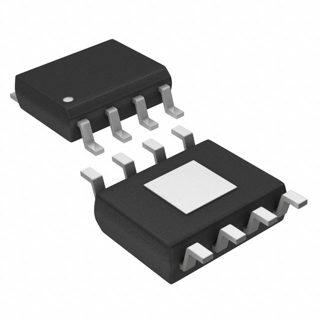
| 产品图片 |
|
| 产品型号 | RT8064ZSP |
| PWM类型 | 电流模式 |
| rohs | 无铅 / 符合限制有害物质指令(RoHS)规范要求 |
| RoHS指令信息 | http://www.richtek.com/download.jsp?t=UyUyRmFzc2V0cyUyRjIwMDklMkYwNiUyRjE3JTJGcGFnZTY1MTYwenRpeGIucGRmJTNEJTNEJTNE%0AR0w5NTI1LUMtLVBiLWZyZWUrUHJvZHVjdCsrR3JlZW4rUHJvZHVjdCtTdGF0ZW1lbnQrMDkwNjE2%0AQw%3D%3D |
| 产品系列 | - |
| 供应商器件封装 | 8-SOP-EP |
| 其它名称 | 1028-1105-6 |
| 包装 | Digi-Reel® |
| 同步整流器 | 是 |
| 安装类型 | 表面贴装 |
| 封装/外壳 | 8-SOIC(0.154",3.90mm 宽)裸焊盘 |
| 工作温度 | -40°C ~ 85°C |
| 标准包装 | 1 |
| 电压-输入 | 2.7 V ~ 5.5 V |
| 电压-输出 | 0.8 V ~ 5 V |
| 电流-输出 | 2A |
| 类型 | 降压(降压) |
| 输出数 | 1 |
| 输出类型 | 可调式 |
| 频率-开关 | 200kHz ~ 2MHz |


- 商务部:美国ITC正式对集成电路等产品启动337调查
- 曝三星4nm工艺存在良率问题 高通将骁龙8 Gen1或转产台积电
- 太阳诱电将投资9.5亿元在常州建新厂生产MLCC 预计2023年完工
- 英特尔发布欧洲新工厂建设计划 深化IDM 2.0 战略
- 台积电先进制程称霸业界 有大客户加持明年业绩稳了
- 达到5530亿美元!SIA预计今年全球半导体销售额将创下新高
- 英特尔拟将自动驾驶子公司Mobileye上市 估值或超500亿美元
- 三星加码芯片和SET,合并消费电子和移动部门,撤换高东真等 CEO
- 三星电子宣布重大人事变动 还合并消费电子和移动部门
- 海关总署:前11个月进口集成电路产品价值2.52万亿元 增长14.8%


PDF Datasheet 数据手册内容提取
® RT8064 2A, 2MHz, Synchronous Step-Down Converter General Description Features The RT8064 is a high efficiency synchronous, step-down (cid:122)(cid:122)(cid:122)(cid:122)(cid:122) High Efficiency : Up to 95% DC/DC converter. Its input voltage range is from 2.7V to (cid:122) Adjustable Frequency : 200kHz to 2MHz 5.5V and provides an adjustable regulated output voltage (cid:122)(cid:122)(cid:122)(cid:122)(cid:122) No Schottky Diode Required from 0.8V to 5V while delivering up to 2A of output current. (cid:122)(cid:122)(cid:122)(cid:122)(cid:122) 0.8V Reference Allows Low Output Voltage Low Dropout Operation : 100% Duty Cycle (cid:122)(cid:122)(cid:122)(cid:122)(cid:122) The internal synchronous low on-resistance power Enable Function (cid:122)(cid:122)(cid:122)(cid:122)(cid:122) switches increase efficiency and eliminate the need for External Soft-Start (cid:122)(cid:122)(cid:122)(cid:122)(cid:122) an external Schottky diode. The default switching Power Good Function (cid:122)(cid:122)(cid:122)(cid:122)(cid:122) frequency is set at 2MHz, if the RT pin is left open. It can RoHS Compliant and Halogen Free (cid:122)(cid:122)(cid:122)(cid:122)(cid:122) also be varied from 200kHz to 2MHz by adding an external resistor. Current mode operation with external Applications compensation allows the transient response to be optimized over a wide range of loads and output capacitors. (cid:122) LCD TV and Monitor Notebook Computers (cid:122) Distributed Power Systems Ordering Information (cid:122) IP Phones (cid:122) RT8064 Digital Cameras Package Type (cid:122) SP : SOP-8 (Exposed Pad-Option 2) QW : WDFN-8L 3x3 (W-Type) Marking Information Lead Plating System RT8064ZSP Z : ECO (Ecological Element with RT8064ZSP : Product Number Halogen Free and Pb free) RT8064 YMDNN : Date Code Note : ZSPYMDNN Richtek products are : (cid:96) RoHS compliant and compatible with the current require- ments of IPC/JEDEC J-STD-020. RT8064ZQW (cid:96) Suitable for use in SnPb or Pb-free soldering processes. 28 : Product Code 28 YM YMDNN : Date Code DNN Copyright © 2012 Richtek Technology Corporation. All rights reserved. is a registered trademark of Richtek Technology Corporation. DS8064-07 November 2012 www.richtek.com 1
RT8064 Pin Configurations (TOP VIEW) COMP 8 PGOOD COMP 1 8 PGOOD SS 2 7 FB SS 2 D 7 FB GND N EN 3 6 RT EN 3 G 6 RT VIN 4 9 5 LX VIN 4 9 5 LX SOP-8 (Exposed Pad) WDFN-8L 3x3 Typical Application Circuit RT8064 L 2.7V to 5V.5IVN 4 VIN LX 5 VOUT R3 1C0INµF R1 100k 7 8 FB COUT PGOOD PGOOD ROSC 6 RT COMP 1 RCOMP R2 CCOMP 9 (Exposed Pad) GND Chip Enable 3 EN SS 2 CSS 10nF Table 1. Recommended Components Selection for f = 1MHz SW V (V) R1 (kΩ) R2 (kΩ) R (kΩ) C (pF) L (μH) C (μF) OUT COMP COMP OUT 3.3 75 24 33 560 2 22 2.5 51 24 22 560 2 22 1.8 30 24 15 560 1.5 22 1.5 21 24 13 560 1.5 22 1.2 12 24 11 560 1.5 22 1 6 24 8.2 560 1.5 22 Copyright © 2012 Richtek Technology Corporation. All rights reserved. is a registered trademark of Richtek Technology Corporation. www.richtek.com DS8064-07 November 2012 2
RT8064 Functional Pin Description Pin No. Pin Name Pin Function SOP-8 WDFN-8L 3x3 (Exposed Pad) Error Amplifier Compensation Point. The current comparator 1 1 COMP threshold increases with this control voltage. Connect external compensation elements to this pin to stabilize the control loop. Soft-Start Control Input. Connect a capacitor from SS to GND to 2 2 SS set the soft-start period. A 10nF capacitor sets the soft-start period to 800μs (typ.). Enable Control Input. Float or connect this pin to logic high for 3 3 EN enable. Connect to GND for disable. 4 4 VIN Power Input Supply. Decouple this pin to GND with a capacitor. Internal Power MOSFET Switches Output. Connect this pin to 5 5 LX the inductor. Oscillator Resistor Input. Connect a resistor from this pin to 6 6 RT GND sets the switching frequency. If this pin is floating, the frequency will be set at 2MHz internally. Feedback. Receives the feedback voltage from a resistive 7 7 FB divider connected across the output. Power Good Indicator. This pin is an open drain logic output that 8 8 PGOOD is pulled to ground when the output voltage is not within ±12.5% of regulation point. Ground. The exposed pad must be soldered to a large PCB and 9 (Exposed Pad) 9 (Exposed Pad) GND connected to GND for maximum power dissipation. Function Block Diagram RT SD VIN ISEN Slope OSC Com COMP 0.8V Output OC EA Limit FB Clamp 10µA Driver SS Hiccup LX Control Logic 0.7V P-G NISEN GND EN Enable 0.4V OTP N-MOSFET ILIM UV PGOOD Copyright © 2012 Richtek Technology Corporation. All rights reserved. is a registered trademark of Richtek Technology Corporation. DS8064-07 November 2012 www.richtek.com 3
RT8064 Absolute Maximum Ratings (Note 1) Supply Input Voltage, VIN --------------------------------------------------------------------------------------- −0.3V to 6V (cid:122) LX Pin Switch Voltage-------------------------------------------------------------------------------------------- −0.3V to (V + 0.3V) (cid:122) IN <10ns ---------------------------------------------------------------------------------------------------------------- −5V to 8.5V Other I/O Pin Voltages------------------------------------------------------------------------------------------- −0.3V to (V + 0.3V) (cid:122) IN LX Pin Switch Current--------------------------------------------------------------------------------------------5A (cid:122) Power Dissipation, P @ T = 25°C (cid:122) D A SOP-8 (Exposed Pad) -------------------------------------------------------------------------------------------1.333W WDFN-8L 3x3 ------------------------------------------------------------------------------------------------------1.429W Package Thermal Resistance (Note 2) (cid:122) SOP-8 (Exposed Pad), θ --------------------------------------------------------------------------------------75°C/W JA SOP-8 (Exposed Pad), θ -------------------------------------------------------------------------------------15°C/W JC WDFN-8L 3x3, θ -------------------------------------------------------------------------------------------------70°C/W JA WDFN-8L 3x3, θ -------------------------------------------------------------------------------------------------8.2°C/W JC Junction Temperature---------------------------------------------------------------------------------------------150°C (cid:122) Lead Temperature (Soldering, 10 sec.)-----------------------------------------------------------------------260°C (cid:122) Storage Temperature Range ------------------------------------------------------------------------------------ −65°C to 150°C (cid:122) ESD Susceptibility (Note 3) (cid:122) HBM (Human Body Model)--------------------------------------------------------------------------------------2kV Recommended Operating Conditions (Note 4) Supply Input Voltage, VIN ---------------------------------------------------------------------------------------2.7V to 5.5V (cid:122) Junction Temperature Range------------------------------------------------------------------------------------ −40°C to 125°C (cid:122) Ambient Temperature Range------------------------------------------------------------------------------------ −40°C to 85°C (cid:122) Electrical Characteristics (VIN = 3.3V, TA= 25°C, unless otherwise specified) Parameter Symbol Test Conditions Min Typ Max Unit Feedback Reference Voltage VREF 0.784 0.8 0.816 V Active , VFB = 0.78V, Not Switching -- 460 -- DC Bias Current μA Shutdown -- -- 10 Output Voltage Line Regulation VIN = 2.7V to 5.5V -- 0.1 -- %/V Output Voltage Load Regulation 0A < ILOAD < 2A -- 0.25 -- % Error Amplifier Trans-conductance gm -- 400 -- μA/V Current Sense Trans-resistance -- 0.3 -- Ω R = 330kΩ 0.8 1 1.2 OSC Switching Frequency MHz Switching 0.2 -- 2 Logic-High V 1.6 -- -- IH EN Input Voltage V Logic-Low V -- -- 0.4 IL Copyright © 2012 Richtek Technology Corporation. All rights reserved. is a registered trademark of Richtek Technology Corporation. www.richtek.com DS8064-07 November 2012 4
RT8064 Parameter Symbol Test Conditions Min Typ Max Unit Switch On-Resistance, High RDS(ON)_P ILX = 0.5A -- 180 250 mΩ Switch On-Resistance, Low RDS(ON)_N ILX = 0.5A -- 120 160 mΩ Peak Current Limit ILIM 2.4 3.5 -- A Under Voltage Lockout VIN Rising -- 2.4 -- V Threshold VIN Falling -- 2.2 -- RT Shutdown Threshold VRT VRT Rising -- VIN − 0.7 VIN − 0.4 V Soft-Start Period t C = 10nF -- 800 -- μs SS SS PGOOD Trip Threshold -- 87.5 -- %V OUT Note 1. Stresses beyond those listed “Absolute Maximum Ratings” may cause permanent damage to the device. These are stress ratings only, and functional operation of the device at these or any other conditions beyond those indicated in the operational sections of the specifications is not implied. Exposure to absolute maximum rating conditions may affect device reliability. Note 2. θJA is measured at TA= 25°C on a high effective thermal conductivity four-layer test board per JEDEC 51-7. θJC is measured at the exposed pad of the package. Note 3. Devices are ESD sensitive. Handling precaution is recommended. Note 4. The device is not guaranteed to function outside its operating conditions. Copyright © 2012 Richtek Technology Corporation. All rights reserved. is a registered trademark of Richtek Technology Corporation. DS8064-07 November 2012 www.richtek.com 5
RT8064 Typical Operating Characteristics Efficiency vs. Output Current Efficiency vs. Output Current 100 100 90 90 80 80 70 70 ) ) % % y ( 60 y ( 60 c c n 50 n 50 e e ci 40 ci 40 Effi Effi 30 30 20 20 10 10 VIN = 5V, VOUT = 1.1V, IOUT = 0A to 2A VIN = 5V, VOUT = 3.3V, IOUT = 0A to 2A 0 0 0 0.5 1 1.5 2 0 0.5 1 1.5 2 Output Current (A) Output Current (A) Output Voltage vs. Output Current Output Voltage vs. Output Current 1.130 3.340 1.120 3.330 V) V) e ( 1.110 e ( 3.320 g g a a olt 1.100 olt 3.310 V V ut ut utp 1.090 utp 3.300 O O 1.080 3.290 VIN = 5V, VOUT = 1.1V, IOUT = 0A to 2A VIN = 5V, VOUT = 3.3V, IOUT = 0A to 2A 1.070 3.280 0 0.5 1 1.5 2 0 0.5 1 1.5 2 Output Current (A) Output Current (A) Switching Frequency vs. Temperature Reference Voltage vs. Temperature 1.04 0.84 1.03 ) 1 0.83 z H 1.02 ) M V 0.82 quency ( 011...900901 Voltage ( 00..8801 e e g Fr 0.98 enc 0.79 chin 0.97 efer 0.78 wit 0.96 R S 0.77 0.95 VIN = 5V, VOUT = 1.1V, IOUT = 0.6A, RRT = 330kΩ VIN = 5V, VOUT = 1.1V 0.94 0.76 -50 -25 0 25 50 75 100 125 -50 -25 0 25 50 75 100 125 Temperature (°C) Temperature (°C) Copyright © 2012 Richtek Technology Corporation. All rights reserved. is a registered trademark of Richtek Technology Corporation. www.richtek.com DS8064-07 November 2012 6
RT8064 V UVLO vs. Temperature Enable Voltage vs. Temperature IN 2.8 1.6 2.7 1.5 2.6 1.4 ) 2.5 V 1.3 V) Rising e ( Rising O ( 2.4 ag 1.2 L 2.3 olt 1.1 V V V UIN 2.2 Falling able 1.0 Falling 2.1 n 0.9 E 2.0 0.8 1.9 0.7 1.8 0.6 -50 -25 0 25 50 75 100 125 -50 -25 0 25 50 75 100 125 Temperature (°C) Temperature (°C) Load Transient Response Load Transient Response VOUT VOUT (100mV/Div) (100mV/Div) IOUT IOUT (1A/Div) VRICNO =M P5 V=, 1V0OkUΩT, =C C1O.1MVP, =IO 5U6T 0=p 1FA to 2A, (1A/Div) VRICNO =M P5 V=, 3V3OkUΩT, =C 3CO.3MVP, =IO 5U6T 0=p 1FA to 2A, Time (100μs/Div) Time (100μs/Div) Switching Switching VLX VLX (5V/Div) (5V/Div) VOUT VOUT (10mV/Div) (10mV/Div) VIN = 5V, VOUT = 1.1V, IOUT = 2A VIN = 5V, VOUT = 3.3V, IOUT = 2A Time (500ns/Div) Time (500ns/Div) Copyright © 2012 Richtek Technology Corporation. All rights reserved. is a registered trademark of Richtek Technology Corporation. DS8064-07 November 2012 www.richtek.com 7
RT8064 Power On from V Power Off from V IN IN VIN VIN (5V/Div) (5V/Div) VOUT VOUT (1V/Div) (1V/Div) VPGOOD VPGOOD (10V/Div) (10V/Div) IOUT IOUT (2A/Div) (2A/Div) VIN = 5V, VOUT = 1.1V, IOUT = 2A, EN = High VIN = 5V, VOUT = 1.1V, IOUT = 2A, EN = High Time (2.5ms/Div) Time (5ms/Div) Power On from EN Power Off from EN VEN VEN (5V/Div) (5V/Div) VOUT VOUT (2V/Div) (2V/Div) VPGOOD VPGOOD (5V/Div) (5V/Div) IOUT IOUT (5A/Div) (5A/Div) VIN = 5V, VOUT = 1.1V, IOUT = 2A VIN = 5V, VOUT = 1.1V, IOUT = 2A Time (500μs/Div) Time (250μs/Div) Copyright © 2012 Richtek Technology Corporation. All rights reserved. is a registered trademark of Richtek Technology Corporation. www.richtek.com DS8064-07 November 2012 8
RT8064 Application Information The basic IC application circuit is shown in Typical Soft-Start Application Circuit. External component selection is The IC contains an external soft-start clamp that gradually determined by the maximum load current and begins with raises the output voltage. The soft-start timing is the selection of the inductor value and operating frequency programmed by the external capacitor between SS pin followed by CIN and COUT. and GND. The chip provides an internal 10μA charge current for the external capacitor. If 10nF capacitor is used to set Main Control Loop the soft-start, the period will be 800μs (typ.). During normal operation, the internal upper power switch (P-MOSFET) is turned on at the beginning of each clock Power Good Output cycle. Current in the inductor increases until the peak The power good output is an open-drain output and requires inductor current reaches the value defined by the output a pull up resistor. When the output voltage is 12.5% above voltage (V ) of the error amplifier. The error amplifier COMP or 12.5% below its set voltage, PGOOD will be pulled adjusts its output voltage by comparing the feedback signal low. It is held low until the output voltage returns to within from a resistive voltage divider on the FB pin with an internal the allowed tolerances once more. During soft-start, 0.8V reference. When the load current increases, it causes PGOOD is actively held low and is only allowed to transition a reduction in the feedback voltage relative to the reference. high when soft-start is over and the output voltage reaches The error amplifier increases its output voltage until the 87.5% of its set voltage. average inductor current matches the new load current. When the upper power MOSFET shuts off, the lower Operating Frequency synchronous power switch (N-MOSFET) turns on until Selection of the operating frequency is a tradeoff between the beginning of the next clock cycle. efficiency and component size. Higher frequency operation allows the use of smaller inductor and capacitor values. Output Voltage Setting Lower frequency operation improves efficiency by reducing The output voltage is set by an external resistive voltage internal gate charge and switching losses but requires divider according to the following equation : larger inductance and/or capacitance to maintain low output ⎛ R1⎞ ripple voltage. VOUT = VREF×⎜1 + ⎟ ⎝ R2⎠ The operating frequency of the IC is determined by an where V equals to 0.8V typical. REF external resistor, R , that is connected between the RT OSC The resistive voltage divider allows the FB pin to sense a pin and ground. The value of the resistor sets the ramp fraction of the output voltage as shown in Figure 1. current that is used to charge and discharge an internal VOUT timing capacitor within the oscillator. The practical switching frequency ranges from 200kHz to 2MHz. However, when R1 the RT pin is floating, the internal frequency is set at 2MHz. FB Determine the RT resistor value by examining the curve RT8064 R2 below. Please notice the minimum on time is about 90ns. GND Figure 1. Setting the Output Voltage Copyright © 2012 Richtek Technology Corporation. All rights reserved. is a registered trademark of Richtek Technology Corporation. DS8064-07 November 2012 www.richtek.com 9
RT8064 2.4 and the power is supplied by a wall adapter through long ) 1 wires, a load step at the output can induce ringing at the z 2.0 H M input. At best, this ringing can couple to the output and y ( 1.6 be mistaken as loop instability. At worst, a sudden inrush c n e of current through the long wires can potentially cause a u q 1.2 re voltage spike at VIN large enough to damage the part. F g hin 0.8 Slope Compensation and Peak Inductor Current c wit 0.4 Slope compensation provides stability in constant S frequency architectures by preventing sub-harmonic 0.0 oscillations at duty cycles greater than 50%. It is 0 300 600 900 1200 1500 1800 2100 accomplished internally by adding a compensating ramp R (k Ω ) RT to the inductor current signal. Normally, the peak inductor Figure 2. Switching Frequency vs. RT Resistor current is reduced when slope compensation is added. For the IC, however, separated inductor current signal is Inductor Selection used to monitor over current condition, so the maximum For a given input and output voltage, the inductor value output current stays relatively constant regardless of the and operating frequency determine the ripple current. The duty cycle. ripple current, ΔI , increases with higher V and decreases L IN Hiccup Mode Under Voltage Protection with higher inductance. A Hiccup Mode Under Voltage Protection (UVP) function ΔIL = ⎛⎜⎝Vf OxU LT ⎞⎟⎠×⎛⎜⎝1−VVOIUNT ⎞⎟⎠ is provided for the IC. When the FB voltage drops below half of the feedback reference voltage, V , the UVP Having a lower ripple current reduces not only the ESR FB function is triggered to auto soft-start the power stage losses in the output capacitors but also the output voltage until this event is cleared. The Hiccup Mode UVP reduces ripple. Highest efficiency operation is achieved by reducing the input current in short circuit conditions, but will not be ripple current at low frequency, but attaining this goal triggered during soft-start process. requires a large inductor. For the ripple current selection, the value of ΔIL= 0.4 (IMAX) Under Voltage Lockout Threshold is a reasonable starting point. The largest ripple current The RT8064 includes an input under voltage lockout occurs at the highest V . To guarantee that the ripple IN protection (UVLO) function. If the input voltage exceeds current stays below a specified maximum value, the the UVLO rising threshold voltage, the converter will reset inductor value needs to be chosen according to the following and prepare the PWM for operation. However, if the input equation : voltage falls below the UVLO falling threshold voltage during L = ⎡ VOUT ⎤×⎡1− VOUT ⎤ normal operation, the device will stop switching. The UVLO ⎢ ⎥ ⎢ ⎥ ⎣f x ΔIL(MAX)⎦ ⎣ VIN(MAX)⎦ rising and falling threshold voltage has a hysteresis to prevent noise caused reset. Using Ceramic Input and Output Capacitors Thermal Considerations Higher values, lower cost ceramic capacitors are now becoming available in smaller case sizes. Their high ripple For continuous operation, do not exceed absolute current, high voltage rating and low ESR make them ideal maximum junction temperature. The maximum power for switching regulator applications. However, care must dissipation depends on the thermal resistance of the IC be taken when these capacitors are used at the input and package, PCB layout, rate of surrounding airflow, and output. When a ceramic capacitor is used at the input difference between junction and ambient temperature. The Copyright © 2012 Richtek Technology Corporation. All rights reserved. is a registered trademark of Richtek Technology Corporation. www.richtek.com DS8064-07 November 2012 10
RT8064 maximum power dissipation can be calculated by the Layout Considerations following formula : Follow the PCB layout guidelines for optimal performance P = (T − T ) / θ of the IC. D(MAX) J(MAX) A JA where TJ(MAX) is the maximum junction temperature, TAis (cid:96) Connect the terminal of the input capacitor (s), CIN, as the ambient temperature, and θ is the junction to ambient close to the VIN pin as possible. This capacitor provides JA thermal resistance. the AC current into the internal power MOSFETs. For recommended operating condition specifications, the (cid:96) LX node experiences high frequency voltage swings so maximum junction temperature is 125°C. The junction to should be kept within a small area. ambient thermal resistance, θJA, is layout dependent. For (cid:96) Keep all sensitive small signal nodes away from the LX SOP-8 (Exposed Pad) packages, the thermal resistance, node to prevent stray capacitive noise pick up. θ , is 75°C/W on a standard JEDEC 51-7 four-layer JA (cid:96) Connect the FB pin directly to the feedback resistors. thermal test board. For WDFN-8L 3x3 packages, the The resistive voltage divider must be connected between thermal resistance, θ , is 70°C/W on a standard JEDEC JA V and GND. OUT 51-7 four-layer thermal test board. The maximum power dissipation at TA = 25°C can be calculated by the following Place the feedback Place the compensation resistors as close to formulas : components as close to the IC as possible the IC as possible P = (125°C − 25°C) / (75°C/W) = 1.333W for D(MAX) GND SOP-8 (Exposed Pad) package R2 CCOMP PD(MAX) = (125°C − 25°C) / (70°C/W) = 1.429W for RCOMPCOMSSP 2 78 PFBGOOD R1 VOUT WDFN-8L 3x3 package GND CSS VEINN 34 956 RLXT RLOXSC shouGldN Dbe connected The maximum power dissipation depends on the operating GND CIN COUT L1 tsoh oinrdt utrcatcoer ,b ayn wd idkeee apn d ambient temperature for fixed T and thermal J(MAX) sensitive components resistance, θJA. The derating curves in Figure 3 allow the VIN VOUT away from this trace Place the input and output capacitors designer to see the effect of rising ambient temperature as close to the IC as possible on the maximum power dissipation. 1.5 Place the feedback W) 1 1.4 Four-Layer PCB Pcolamcpeo tnheen ctos masp ecnlossaeti oton rtheesi sICto arss apso cslsoibsele to n ( 11..23 the IC as possible o ati 1.1 GND p 1.0 ssi 0.9 WDFN-8L 3x3 CCOMP R2 Di 0.8 COMP 1 8 PGOOD R1 er 0.7 RCOMP SS 2 ND 7 FB VOUT ow 0.6 SOP-8 (Exposed Pad) CSS VEINN 34 G9 65 RLXT ROSC GND P 0.5 LX should be connected mum 00..34 GND CIN COUT L1 tsoh oinrdt utrcatcoer ,b ayn wd ikdeee apn d sensitive components axi 0.2 VIN VOUT away from this trace M 0.1 Place the input and output capacitors 0.0 as close to the IC as possible 0 25 50 75 100 125 Figure 4. PCB Layout Guide Ambient Temperature (°C) Figure 3. Derating Curve of Maximum Power Dissipation Copyright © 2012 Richtek Technology Corporation. All rights reserved. is a registered trademark of Richtek Technology Corporation. DS8064-07 November 2012 www.richtek.com 11
RT8064 Outline Dimension H A M EXPOSED THERMAL PAD Y (Bottom of Package) J X B F C I D Dimensions In Millimeters Dimensions In Inches Symbol Min Max Min Max A 4.801 5.004 0.189 0.197 B 3.810 4.000 0.150 0.157 C 1.346 1.753 0.053 0.069 D 0.330 0.510 0.013 0.020 F 1.194 1.346 0.047 0.053 H 0.170 0.254 0.007 0.010 I 0.000 0.152 0.000 0.006 J 5.791 6.200 0.228 0.244 M 0.406 1.270 0.016 0.050 X 2.000 2.300 0.079 0.091 Option 1 Y 2.000 2.300 0.079 0.091 X 2.100 2.500 0.083 0.098 Option 2 Y 3.000 3.500 0.118 0.138 8-Lead SOP (Exposed Pad) Plastic Package Copyright © 2012 Richtek Technology Corporation. All rights reserved. is a registered trademark of Richtek Technology Corporation. www.richtek.com DS8064-07 November 2012 12
RT8064 D2 D L E E2 SEE DETAIL A 1 e b 2 1 2 1 A A3 A1 DETAIL A Pin #1 ID and Tie Bar Mark Options Note : The configuration of the Pin #1 identifier is optional, but must be located within the zone indicated. Dimensions In Millimeters Dimensions In Inches Symbol Min Max Min Max A 0.700 0.800 0.028 0.031 A1 0.000 0.050 0.000 0.002 A3 0.175 0.250 0.007 0.010 b 0.200 0.300 0.008 0.012 D 2.950 3.050 0.116 0.120 D2 2.100 2.350 0.083 0.093 E 2.950 3.050 0.116 0.120 E2 1.350 1.600 0.053 0.063 e 0.650 0.026 L 0.425 0.525 0.017 0.021 W-Type 8L DFN 3x3 Package Richtek Technology Corporation 5F, No. 20, Taiyuen Street, Chupei City Hsinchu, Taiwan, R.O.C. Tel: (8863)5526789 Richtek products are sold by description only. Richtek reserves the right to change the circuitry and/or specifications without notice at any time. Customers should obtain the latest relevant information and data sheets before placing orders and should verify that such information is current and complete. Richtek cannot assume responsibility for use of any circuitry other than circuitry entirely embodied in a Richtek product. Information furnished by Richtek is believed to be accurate and reliable. However, no responsibility is assumed by Richtek or its subsidiaries for its use; nor for any infringements of patents or other rights of third parties which may result from its use. No license is granted by implication or otherwise under any patent or patent rights of Richtek or its subsidiaries. DS8064-07 November 2012 www.richtek.com 13