ICGOO在线商城 > 传感器,变送器 > 位置传感器 - 角,线性位置测量 > KMA210:115
 Datasheet下载
- 型号: KMA210:115
- 制造商: NXP Semiconductors
- 库位|库存: xxxx|xxxx
- 要求:
| 数量阶梯 | 香港交货 | 国内含税 |
| +xxxx | $xxxx | ¥xxxx |
查看当月历史价格
查看今年历史价格
KMA210:115产品简介:
ICGOO电子元器件商城为您提供KMA210:115由NXP Semiconductors设计生产,在icgoo商城现货销售,并且可以通过原厂、代理商等渠道进行代购。 KMA210:115价格参考。NXP SemiconductorsKMA210:115封装/规格:位置传感器 - 角,线性位置测量, Magnetoresistive Sensor Angle External Magnet, Not Included PC Pin。您可以下载KMA210:115参考资料、Datasheet数据手册功能说明书,资料中有KMA210:115 详细功能的应用电路图电压和使用方法及教程。
NXP USA Inc.生产的KMA210:115是一款基于磁阻技术的位置传感器,主要用于角位置和线性位置测量。以下是其主要应用场景:

 1. 汽车行业
   - 电机控制:用于无刷直流电机(BLDC)的转子位置检测,实现精确的换向控制。
   - 转向系统:在电动助力转向(EPS)中,用于检测方向盘的角度和旋转方向。
   - 油门踏板位置监测:实时监测油门踏板的角度变化,确保驾驶安全。
   - 变速器位置检测:用于自动变速箱或手动变速箱中的档位位置检测。

 2. 工业自动化
   - 机器人关节角度测量:在工业机器人中,用于检测机械臂关节的旋转角度,实现精准运动控制。
   - 伺服电机反馈:为伺服控制系统提供高精度的转子位置信息,提升系统性能。
   - 线性滑轨位置检测:通过磁性编码器测量滑轨的线性位移,适用于精密加工设备。

 3. 消费电子
   - 家用电器:如洗衣机、空调等设备中,用于检测风扇或电机的转速和角度。
   - 游戏设备:用于体感控制器或虚拟现实(VR)设备中的位置追踪。

 4. 医疗设备
   - 医疗器械控制:如手术机器人、康复设备中,用于精确的角度和位置测量。
   - 呼吸机和泵:监测关键部件的运行状态,确保设备正常工作。

 5. 航空航天与国防
   - 飞行控制系统:用于无人机、飞机等的舵面角度检测。
   - 惯性导航系统:辅助测量旋转角度和线性位移。

 6. 其他应用
   - 智能家居:如智能锁、百叶窗等设备中,用于检测开关状态或角度变化。
   - 能源管理:风力发电机叶片角度检测,优化发电效率。

KMA210:115凭借其高精度、低功耗和非接触式测量的特点,在上述领域中表现出色,能够满足各种严苛环境下的位置测量需求。
| 参数 | 数值 |
| 产品目录 | |
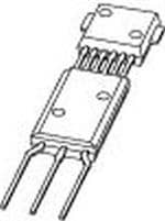
| 描述 | MOD MAGNET ANGLE SENSOR SOT1288 |
| 产品分类 | |
| 品牌 | NXP Semiconductors |
| 数据手册 | |
| 产品图片 |
|
| 产品型号 | KMA210:115 |
| rohs | 无铅 / 符合限制有害物质指令(RoHS)规范要求 |
| 产品系列 | KMA |
| 其它名称 | 568-8399-2 |
| 安装类型 | 通孔 |
| 工作温度 | -40°C ~ 160°C |
| 技术 | 磁阻 |
| 旋转角度 | 180° |
| 标准包装 | 1,800 |
| 用于测量 | 角度 |
| 电压-电源 | 4.5 V ~ 5.5 V |
| 电阻(Ω) | - |
| 电阻容差 | - |
| 端子类型 | PC 引脚 |
| 线性度 | ±1.2° |
| 线性范围 | - |
| 致动器类型 | 外磁铁,不含 |


- 商务部:美国ITC正式对集成电路等产品启动337调查
- 曝三星4nm工艺存在良率问题 高通将骁龙8 Gen1或转产台积电
- 太阳诱电将投资9.5亿元在常州建新厂生产MLCC 预计2023年完工
- 英特尔发布欧洲新工厂建设计划 深化IDM 2.0 战略
- 台积电先进制程称霸业界 有大客户加持明年业绩稳了
- 达到5530亿美元!SIA预计今年全球半导体销售额将创下新高
- 英特尔拟将自动驾驶子公司Mobileye上市 估值或超500亿美元
- 三星加码芯片和SET,合并消费电子和移动部门,撤换高东真等 CEO
- 三星电子宣布重大人事变动 还合并消费电子和移动部门
- 海关总署:前11个月进口集成电路产品价值2.52万亿元 增长14.8%

PDF Datasheet 数据手册内容提取
KMA210 Programmable angle sensor Rev. 2 — 7 December 2011 Product data sheet 1. Product profile 1.1 General description The KMA210 is a magnetic angle sensor module. The MagnetoResistive (MR) sensor bridges, the mixed signal Integrated Circuit (IC) and the required capacitances are integrated into a single package. This angular measurement module KMA210 is pre-programmed, pre-calibrated and therefore, ready to use. The KMA210 allows user-specific adjustments of angular range, zero angle and clamping voltages. The settings are stored permanently in a non-volatile memory. 1.2 Features and benefits High precision sensor for magnetic High temperature range up to 160C angular measurement Single package sensor module with Ratiometric analog output voltage integrated filters for improved ElectroMagnetic Compatibility (EMC) Automotive qualified in accordance with Overvoltage protection up to 16V AEC-Q100Rev-G Programmable user adjustments, Programming via One-Wire Interface including zero angle and angular range (OWI) Fail-safe non-volatile memory with write User-programmable 32-bit identifier protection using lock bit Independent from magnetic field Magnet-loss, power-loss and broken strength above 35kA/m bond wire detection Ready to use without external Factory calibrated components
KMA210 NXP Semiconductors Programmable angle sensor 2. Pinning information Table 1. Pinning Pin Symbol Description Simplified outline 1 V supply voltage DD 2 GND ground 3 OUT/DATA analog output or data interface 1 2 3 3. Ordering information Table 2. Ordering information Type number Package Name Description Version KMA210 - plastic single-ended multi-chip package; SOT1288 6interconnections; 3 in-line leads KMA210 All information provided in this document is subject to legal disclaimers. © NXP B.V. 2011. All rights reserved. Product data sheet Rev. 2 — 7 December 2011 2 of 37
xxxx xxxxxxxxxxxxxxxxxxxxxxxxxxxxxx x xxxxxxxxxxxxxx xxxxxxxxxx xxx xxxxxx xxxxxxxxxxxxxxxxxxxxxxx xxxxxxxxxxxxxxxxxxxxxx xxxxx xxxxxx xx xxxxxxxxxxxxxxxxxxxxxxxxxxxxx xxxxxxxxxxxxxxxxxxxxxx xxxxxxxxxxx xxxxxxx xxxxxxxxxxxxxxxxxxx xxxxxxxxxxxxxxxx xxxxxxxxxxxxxx xxxxxx xx xxxxxxxxxxxxxxxxxxxxxxxxxxxxxxxx xxxxxxxxxxxxxxxxxxxxxxxx xxxxxxx xxxxxxxxxxxxxxxxxxxxxxxxxxxxxxxxxxxxxxxxxxxxxx xxxxxxxxxxx xxxxx x x P K 4 N rodu MA210 . XP ct da Fu Se ta n m sheet ctio icon n d a u l c d t o ia r s g VDD r a ANALOG ANALOG DIGITAL m VOLTAGE VOLTAGE VOLTAGE UNDERVOLTAGE REGULATOR REGULATOR REGULATOR DETECTION/ (CLEAN) (SWITCHING) POR POR A ll inform PDOEWTEERC-TLIOOSNS PDOEWTEERC-TLIOOSNS Cblock Rev. 2 — 7 December 2011 ation provided in this document is subject to legal disclaimers. NOMN-EVMOGOLNRATDYILLLEOOFFWWIILL--TTPPEEAARRSSSS COTNEMULTIPLEXER (MUX)TSRTOdLifafemrepnliftiieaGrlECNLEORCATKOARDC DEMUX AFVILDETIRGEOARISTG ACAILNNILDGLATOR COORFRFESCETTIODNAC CALACNUGLLAEobTuuIOtffpeuNrt ADAJRNUAGSNUTGLMAEERNT GND IIONNTTNSEEEERRR-WFFIAAAIRLCCEEE CL OUT/DATA GND MAGNETORESISTIVE INTEGRATED SENSOR BRIDGES SIGNAL CONDITIONING INTEGRATED CIRCUIT CAPACITANCES 001aan661 P r o g r a m m © N ab K XP le B.V. 2011. A angle MA 3 of 37 ll rights reserved. Fig 1. Functional diagram of KMA210 sensor 210
KMA210 NXP Semiconductors Programmable angle sensor 5. Functional description The KMA210 amplifies two orthogonal differential signals from MR sensor bridges and converts them into the digital domain. The angle is calculated using the COordinate Rotation DIgital Computer (CORDIC) algorithm. After a digital-to-analog conversion the analog signal is provided to the output as a linear representation of the angular value. Zero angle, clamping voltages and angular range are programmable. In addition, two 16-bit registers are available for customer purposes, such as sample identification. The KMA210 comprises a Cyclic Redundancy Check (CRC) and an Error Detection and Correction (EDC), as well as magnet-loss and broken bond wire detection to ensure afail-safe operation. A power-loss detection circuit pulls the analog output to the remaining connection, if either the supply voltage or the ground line of the mixed signal IC is interrupted. After multiplexing the two MR Wheatstone bridge signals and their successive amplification, the signal is converted into the digital domain by an Analog-to-Digital Converter (ADC). Further processing is done within an on-chip state machine. This includes offset cancellation, calculation of the mechanical angle using the CORDIC algorithm, as well as zero angle and angular range adjustment. The internal Digital-to-Analog Converter (DAC) and the analog output stage are used for conversion of the angle information into an analog output voltage, which is ratiometric to the supply voltage. The configuration parameters are stored in a user-programmable non-volatile memory. The OWI (accessible using pin OUT/DATA) is used for accessing the memory. In order to protect the memory content a lock bit can be set. After locking the non-volatile memory, itscontent cannot be changed anymore. 5.1 Angular measurement directions The differential signals of the MR sensor bridges depend only on the direction of the external magnetic field strength H , which is applied parallel to the plane of the sensor. ext Inorder to obtain a correct output signal, the minimum saturation field strength has to be exceeded. KMA210 All information provided in this document is subject to legal disclaimers. © NXP B.V. 2011. All rights reserved. Product data sheet Rev. 2 — 7 December 2011 4 of 37
KMA210 NXP Semiconductors Programmable angle sensor α Hext 001aan665 Fig 2. Angular measurement directions Since the Anisotropic MR (AMR) effect is periodic over 180, the sensor output is also 180-periodic, where the angle is calculated relative to a freely programmable zero angle. The dashed line indicates the mechanical zero degree position. 6. Analog output The KMA210 provides one analog output signal on pin OUT/DATA. The measured angle is converted linearly into a value, which is ratiometric to the supply voltage V . Either a DD positive or a negative slope is provided for this purpose. Table3 describes the analog output behavior for a positive slope. If for example, amagnetic field angle, above the programmed maximum angle , but below the clamp max switch angle is applied to the sensor, then analog output is set to the upper sw(CL) clamping voltage. If the magnetic field angle is larger than the clamp switch angle, the analog output switches from upper to lower clamping voltage. In the case of a negative slope, the clamping voltages are changed. Table 3. Analog output behavior for a positive slope Magnetic field angle Analog output < < V max sw(CL) (CL)u < < + 180 V sw(CL) ref (CL)l The analog output voltage range encodes both angular and diagnostic information. A valid angle value is between the upper and lower clamping voltage. If the analog output is in the diagnostic range, that is below 4%V or above 96%V , an error condition has been DD DD detected. The analog output repeats every 180. KMA210 All information provided in this document is subject to legal disclaimers. © NXP B.V. 2011. All rights reserved. Product data sheet Rev. 2 — 7 December 2011 5 of 37
KMA210 NXP Semiconductors Programmable angle sensor VO (%VDD) αrng V(CL)u V(CL)I 0 αref αmax 180 α (deg) α sw(CL) αref + 180° 001aag811 max=ref+rng Fig 3. Characteristic of the analog output 7. Diagnostic features The KMA210 provides several diagnostic features: 7.1 CRC and EDC supervision The KMA210 includes a supervision of the programmed data. At power-on, a CRC of the non-volatile memory is performed. Furthermore the memory is protected against bit errors. Every 16-bit data word is saved internally as a 22-bit word for this purpose. The protection logic corrects any single-bit error in a data word, while the sensor continues in normal operation mode. Double-bit errors per word will be detected and switches the device into diagnostic mode. 7.2 Magnet-loss detection If the applied magnetic field strength is not sufficient, the KMA210 can raise a diagnostic condition. In order to enter the diagnostic mode, due to magnet-loss, the detection has to be enabled first. The device can be programmed into active diagnostic mode, where the output is driven below 4%V or above 96%V . DD DD 7.3 Power-loss detection The power-loss detection circuit enables the detection of an interrupted supply or ground line of the mixed signal IC in normal operation mode up to the maximum operating supply voltage. In the case of a power-loss condition, two internal switches in the sensor are closed, connecting the pin of the analog output to the supply voltage and the ground pins. KMA210 All information provided in this document is subject to legal disclaimers. © NXP B.V. 2011. All rights reserved. Product data sheet Rev. 2 — 7 December 2011 6 of 37
KMA210 NXP Semiconductors Programmable angle sensor KMA210 VDD ZO(pl) OUT/DATA ZO(pl) GND 008aaa259 Fig 4. Equivalent output circuit in case of a power-loss condition Table4 describes the power-loss behavior and gives the resulting output voltage depending on the interrupted supply or ground line and the load resistance. T able 4. Power-loss behavior Load resistance Interrupted supply line Interrupted ground line R >5k V 4%V V 96%V L(ext) O DD O DD 7.4 Broken bond wire detection The broken bond wire detection circuit enables the detection of an interrupted supply or ground line of the MR sensor bridge. In the case of a broken bond wire the device goes into diagnostic mode and a status bit is set. 7.5 Low supply voltage detection and overvoltage protection If the supply voltage is below the switch-off threshold voltage, a status bit is set and the device goes into diagnostic mode. If the supply voltage is above the overvoltage switch-on threshold voltage, the device enters diagnostic mode. Table5 describes the system behavior depending on the voltage range of the supply voltage. Table 5. System behavior Supply voltage State Description 0V to 1.8V start-up power The output buffer drives an active LOW or is powered down, but the switches of the power-loss detection circuit are not fully opened and set the output to a level between ground and half the supply voltage. 1.8V to V power-on The power-loss charge pump is fully operational and turns the POR reset switches of the detection circuit off. The output buffer drives an active LOW and sets the output to the lower diagnostic level. During the reset phase all circuits are in reset and/or Power-down mode. V to V or initialization The digital core and the oscillator are active. After reset the POR th(on) V content of the non-volatile memory is copied into the shadow th(off) registers. The output buffer drives an active LOW and sets the output to the lower diagnostic level. V or V to functional All analog circuits are active and the measured angle is th(on) th(off) minimum V operation available at the analog output. Not all parameters are within DD the specified limits. KMA210 All information provided in this document is subject to legal disclaimers. © NXP B.V. 2011. All rights reserved. Product data sheet Rev. 2 — 7 December 2011 7 of 37
KMA210 NXP Semiconductors Programmable angle sensor Table 5. System behavior …continued Supply voltage State Description Minimum V to normal All analog circuits are active and the measured angle is DD maximum V operation available at the analog output. All parameters are within the DD specified limits. Maximum V to functional All analog circuits are active and the measured angle is DD V operation available at the analog output. Not all parameters are within th(ov) the specified limits. V to 16V overvoltage The digital core and the oscillator are active but all other th(ov) circuits are in Power-down mode. The output is set to the lower diagnostic level. Table6 describes the diagnostic behavior and the resulting output voltage depending on the error case. Furthermore the duration and termination condition to enter and leave the diagnostic mode are given, respectively. Table 6. Diagnostic behavior Diagnostic condition Duration Analog output Termination condition Low voltage 1s<t<10s 4%V functional or normal DD operation Overvoltage 1s<t<10s 4%V functional or normal DD operation Checksum error n/a 4%V or 96%V [2] power-on reset[1] DD DD Double-bit error n/a 4%V or 96%V [2] power-on reset[1] DD DD Magnet-loss 0.5ms<t<6ms 4%V or 96%V [2] magnet present[1] DD DD Power-loss 2ms 4%V or 96%V [2] power-on reset DD DD Broken bond wire 0.2ms<t<1ms 4%V or 96%V [2] power-on reset[1] DD DD [1] Status bit stays set in command register until power-on reset. [2] Depending on the diagnostic level setting. 8. Limiting values Table 7. Limiting values In accordance with the Absolute Maximum Rating System (IEC 60134). Symbol Parameter Conditions Min Max Unit V supply voltage 0.3 +16 V DD V output voltage 0.3 +16 V O V overvoltage output voltage T <140C [1] V 16 V O(ov) amb th(ov) at t<1h I reverse current T <70C - 150 mA r amb T ambient temperature 40 +160 C amb T programming ambient temperature 10 70 C amb(pr) T storage temperature 40 +125 C stg Non-volatile memory t data retention time T =50C 17 - year ret(D) amb N write or erase endurance T =70C 100 - cycle endu(W_ER) amb(pr) [1] Overvoltage on analog output and supply within the specified operating voltage range. KMA210 All information provided in this document is subject to legal disclaimers. © NXP B.V. 2011. All rights reserved. Product data sheet Rev. 2 — 7 December 2011 8 of 37
KMA210 NXP Semiconductors Programmable angle sensor 9. Recommended operating conditions Table 8. Operating conditions In a homogenous magnetic field. Symbol Parameter Conditions Min Typ Max Unit V supply voltage [1] 4.5 5.0 5.5 V DD T ambient temperature 40 - +160 C amb T programming ambient temperature 10 - 70 C amb(pr) C external load capacitance [1][2] 0 - 22 nF L(ext) [2][3] 0 - 6.8 nF R external load resistance [4] 5 - k L(ext) H external magnetic field strength 35 - - kA/m ext [1] Normal operation mode. [2] Between ground and analog output. [3] Command mode. [4] Power-loss detection is only possible with a load resistance within the specified range connected to the supply or ground line. 10. Thermal characteristics Table 9. Thermal characteristics Symbol Parameter Conditions Typ Unit R thermal resistance from junction to 145 K/W th(j-a) ambient 11. Characteristics Table 10. Supply current Characteristics are valid for the operating conditions, as specified in Section9. Symbol Parameter Conditions Min Typ Max Unit I supply current [1][2] 5 - 10.5 mA DD [3][4] - - 13 mA I overvoltage switch-off current [5] - - 6 mA off(ov) [1] Normal operation and diagnostic mode excluding overvoltage and undervoltage within the specified operating supply voltage range. [2] Without load current at the analog output. [3] Normal operation and diagnostic mode over full voltage range up to limiting supply voltage at steady state. [4] With minimum load resistance at the analog output. [5] Diagnostic mode for a supply voltage above the overvoltage threshold voltage up to the limiting supply voltage. KMA210 All information provided in this document is subject to legal disclaimers. © NXP B.V. 2011. All rights reserved. Product data sheet Rev. 2 — 7 December 2011 9 of 37
KMA210 NXP Semiconductors Programmable angle sensor Table 11. Power-on res et Characteristics are valid for the operating conditions, as specified in Section9. Symbol Parameter Conditions Min Typ Max Unit V switch-on threshold analog output switches on, if - 4.30 4.45 V th(on) voltage V >V DD th(on) V switch-off threshold analog output switches off, if 3.90 4.10 - V th(off) voltage V <V DD th(off) V hysteresis voltage V =V V 0.1 0.2 - V hys hys th(on) th(off) V power-on reset voltage IC is initialized - 3.3 3.6 V POR V overvoltage threshold analog output switches off, if 6.5 7.5 8.0 V th(ov) voltage V >V DD th(ov) V overvoltage hysteresis 0.1 0.3 - V hys(ov) voltage Table 12. Module perfo rmance Characteristics are valid for the operating conditions, as specified in Section9. Symbol Parameter Conditions Min Typ Max Unit angle resolution [1] - - 0.04 deg res maximum angle programmable angular range [2] 5 - 180 deg max for V V 80%V (CL)u (CL)l DD reference angle programmable zero angle [2] 0 - 180 deg ref V nominal output voltage at full supply operating range 5 - 95 %V O(nom) DD V upper diagnostic range [3][4][5] 96 - 100 %V O(udr) DD output voltage V lower diagnostic range [3][4][5] 0 - 4 %V O(ldr) DD output voltage V upper clamping voltage [4][5][6] 40 - 95 %V (CL)u DD V lower clamping voltage [4][5][6] 5 - 30.5 %V (CL)l DD V clamping voltage variation deviation from programmed [4][5] 0.3 - +0.3 %V (CL) DD value V RMS output noise voltage equivalent power noise [1][4] - 0.4 2.5 mV n(o)(RMS) linearity error temperature range [4][7] 1.2 - +1.2 deg lin 40Cto+160C temperature range [4][7] 1 - +1 deg 40Cto+140C temperature drift error temperature range [1][4][7] - - 0.8 deg temp 40Cto+160C [8] temperature range [1][4][7] - - 0.65 deg 40Cto+140C [8] temperature drift error at temperature range [7][8][9] - - 0.65 deg tempRT room temperature 40Cto+160C temperature range [7][8][9] - - 0.55 deg 40Cto+140C hysteresis error referred to input [4][7] - - 0.09 deg hys microlinearity error referred to input [4][7] 0.1 - +0.1 deg lin KMA210 All information provided in this document is subject to legal disclaimers. © NXP B.V. 2011. All rights reserved. Product data sheet Rev. 2 — 7 December 2011 10 of 37
KMA210 NXP Semiconductors Programmable angle sensor Table 12. Module performance …continued Characteristics are valid for the operating conditions, as specified in Section9. Symbol Parameter Conditions Min Typ Max Unit angular error temperature range [4][7] 1.35 - +1.35 deg ang 40Cto+160C [10] temperature range [4][7] 1.1 - +1.1 deg 40Cto+140C [10] m slope of angular error [4][7] - - 0.04 deg/deg ang [10] Z power-loss output impedance to remaining - - 210 O(pl) impedance supply line in case of lost supply voltage or lost ground [1] At a nominal output voltage between 5%VDD and 95%VDD and a maximum angle of max=180. [2] In steps of resolution <0.022. [3] Activation is dependent on the programmed diagnostic mode. [4] At a low-pass filtered analog output with a cut-off frequency of 0.7kHz. [5] Settling to these values is limited by 0.7kHz low-pass filtering of analog output. [6] In steps of 0.02%V . DD [7] Definition of errors is given in Section12. [8] Based on a 3 standard deviation. [9] Room temperature is given for an ambient temperature of 25C. [10] Graph of angular error is shown in Figure5. 1.40 1.35 |Δφang| (deg) 1.10 (1) (2) 0.75 0.65 0 −20 −16 −12.25 −10 1 12.25 16 20 α1 − α0 (deg) 001aal765 (1) 40C to +160C (2) 40C to +140C Fig 5. Envelope curve for the magnitude of angular error KMA210 All information provided in this document is subject to legal disclaimers. © NXP B.V. 2011. All rights reserved. Product data sheet Rev. 2 — 7 December 2011 11 of 37
KMA210 NXP Semiconductors Programmable angle sensor Table 13. Dynamics Characteristics are valid for the operating conditions, as specified in Section9. Symbol Parameter Conditions Min Typ Max Unit t turn-on time until first valid result - - 5 ms on f update frequency 2.4 3.125 - kHz upd t settling time after an ideal mechanical - - 1.8 ms s angle step of 45, until 90% of the final value is reached t enter command mode time after power on 20 - 30 ms cmd(ent) t overvoltage recovery time after overvoltage - - 4 ms rec(ov) Table 14. Digital interf ace Characteristics are valid for the operating conditions, as specified in Section9. Symbol Parameter Conditions Min Typ Max Unit V HIGH-level input voltage 80 - - %V IH DD V LOW-level input voltage - - 20 %V IL DD V HIGH-level output voltage I =2mA 80 - - %V OH O DD V LOW-level output voltage I =2mA - - 20 %V OL O DD I overdrive current absolute value for overdriving - - 20 mA od the output buffer t start time LOW level before rising edge 5 - - s start t stop time HIGH level before falling edge 5 - - s stop T bit period minimum period may be 10 - 100 s bit limited by the load capacitance T bit period deviation deviation between received 0.8T 1T 1.2T s bit bit bit bit clock and sent clock t pulse width0 0.175T 0.25T 0.375T s w0 bit bit bit t pulse width1 0.625T 0.75T 0.825T s w1 bit bit bit t time-out time communication reset - - 220 s to guaranteed after maximum t to t slave takeover time duration of LOW level for 1 - 5 s tko(slv) slave takeover t master takeover time duration of LOW level for 0T - 0.5T s tko(mas) bit bit master takeover t programming time for a single memory address 20 - - ms prog t charge pump time waiting time after enabling the 1 - - ms cp non-volatile memory charge pump clock Table 15. Internal capa citances Characteristics are valid for the operating conditions, as specified in Section9. Symbol Parameter Conditions Min Typ Max Unit C blocking capacitance [1] 25 47 75 nF block C load capacitance [1] 1.1 2.2 3.3 nF L [1] Measured at 1MHz. KMA210 All information provided in this document is subject to legal disclaimers. © NXP B.V. 2011. All rights reserved. Product data sheet Rev. 2 — 7 December 2011 12 of 37
KMA210 NXP Semiconductors Programmable angle sensor 12. Definition of errors 12.1 General Angular measurement errors by the KMA210 result from linearity errors, temperature drift errors and hysteresis errors. Figure6 shows the output signal of an ideal sensor, where the measured angle corresponds ideally to the magnetic field angle . This curve meas will further be denoted as angle reference line () with a slope of 0.5%V /degree. ref DD φ meas (deg) φref(α) 180 α (deg) 001aag812 Fig 6. Definition of the reference line The angular range is set to =180 and the clamping voltages are programmed to max V =5%V and V =95%V for a valid definition of errors. (CL)l DD (CL)u DD 12.2 Hysteresis error The hysteresis error is defined as the maximum difference between the angles, hys given by the device output when performing a positive (clockwise) rotation and negative (counter clockwise) rotation over an angular range of 180, measured at a constant temperature. φ meas (deg) Δφ hys 180 α (deg) 001aag813 Fig 7. Definition of the hysteresis error Equation1 gives the mathematical description for the hysteresis value : hys () = (180)– (0) (1) hys meas meas KMA210 All information provided in this document is subject to legal disclaimers. © NXP B.V. 2011. All rights reserved. Product data sheet Rev. 2 — 7 December 2011 13 of 37
KMA210 NXP Semiconductors Programmable angle sensor 12.3 Linearity error The KMA210 output signal deviation from a best straight line , with the same slope as BSL the reference line, is defined as linearity error. The magnetic field angle is varied at fixed temperatures for measurement of this linearity error. The output signal deviation from the best straight line at the given temperature is the linearity error . It is a function of the lin magnetic field angle and the temperature of the device T . amb φ meas (deg) φBSL(α, Tamb) φref(α) Δφlin(α, Tamb) 180 α (deg) 001aag814 Fig 8. Definition of the linearity error 12.4 Microlinearity error The microlinearity error is the device output deviation from 1, if the magnetic field lin angle is changed by =1. φ meas (deg) φref(α) Δφmeas = 1° + Δφμlin(α) α (deg) Δα = 1° 001aag815 Fig 9. Definition of the microlinearity error 12.5 Temperature drift error The temperature drift is defined as the envelope over the deviation of the angle temp versus the temperature range. It is considered as the pure thermal effect. KMA210 All information provided in this document is subject to legal disclaimers. © NXP B.V. 2011. All rights reserved. Product data sheet Rev. 2 — 7 December 2011 14 of 37
KMA210 NXP Semiconductors Programmable angle sensor φ meas (deg) Ty Tx Δφ temp 180 α (deg) 001aag816 Fig 10. Definition of the temperature drift error Equation2 gives the mathematical description for temperature drift value : temp () = (, T )– (, T ) (2) temp meas x meas y with: T : temperature for maximum at angle x meas T : temperature for minimum at angle y meas The deviation from the value at room temperature describes the temperature tempRT drift of the angle, compared to the value, which the sensor provides at room temperature: (, T ) = (, T )– (, T ) (3) temp RT amb meas amb meas RT with: T : room temperature (25C) RT 12.6 Angular error The angular error is the error of angle difference measured by the sensor, if the ang mechanical angle deviates from to . Here and are arbitrary angles within the 0 1 0 1 angular range. The angle measurement at is the initially programmed reference angle, 0 programmed by the customer at room temperature and zero hour upon production. The angle measurement at is made at any temperature within the ambient temperature 1 range: = ( , T )– ( , T )– – (4) ang meas 1 amb meas 0 RT 1 0 with: , : arbitrary mechanical angles within the angular range 0 1 ( , T ): programmed angle at , T =25C and zero hour upon production meas 0 RT 0 RT ( , T ): angle measured by the sensor at and any temperature within T meas 1 amb 1 amb This error comprises non-linearity and temperature drift related to the room temperature. KMA210 All information provided in this document is subject to legal disclaimers. © NXP B.V. 2011. All rights reserved. Product data sheet Rev. 2 — 7 December 2011 15 of 37
KMA210 NXP Semiconductors Programmable angle sensor |Δφang| mang |Δφang(peak)| |Δφμlin + Δφtemp|RT| −α* α0 − 1° α0 + 1° +α* α α 1 0 001aal766 Fig 11. Envelope curve for the magnitude of angular error Figure11 shows the envelope curve for the magnitude of angular error | | versus ang 1 for all angles and all temperatures T within the ambient temperature range. | | 0 amb ang has its minimum, if is in the range of 1 around . Here only the microlinearity error 1 0 and the temperature drift related to the room temperature | | occurs. If lin tempRT 1 deviates from by more than 1 in either direction, | | can increase with a gradient 0 ang defined by slope m . ang Angular error can be expressed by Equation5 to Equation8: for | |1 1 0 = + (5) ang lin temp RT for 1<| |<* 1 0 = + +m – –1 (6) ang lin temp RT ang 1 0 for | |* 1 0 = 2+ 2 (7) ang lin temp RT with: – + = ---------a--n--g--(--p--e--a--k--)---------------------l--i-n----------------t--e--m----p----R---T---+ +1 (8) m 0 ang 13. Programming 13.1 General description The KMA210 provides an OWI to enable programming of the device which uses pinOUT/DATA bidirectionally. In general the device runs in analog output mode, the normal operation mode. This mode is configured by the embedded programming data and is started after a power-on reset once time t has elapsed. In this mode, the magnetic field angle is converted into the on corresponding output voltage. KMA210 All information provided in this document is subject to legal disclaimers. © NXP B.V. 2011. All rights reserved. Product data sheet Rev. 2 — 7 December 2011 16 of 37
KMA210 NXP Semiconductors Programmable angle sensor Command mode has to be entered to enable programming. In this mode, the customer can adjust all required parameters (for example zero angle and angular range) to meet the application requirements. After enabling the internal charge pump and waiting for t the cp data is stored in the non-volatile memory. After changing the contents of the memory, the checksum must be recalculated and written (seeSection13.4). In order to enter the command mode, a specific command sequence must be sent after a power-on reset and during the time slot t . The external source used to send the cmd(ent) command sequence must overdrive the output buffer of the KMA210. In doing so it provides current I . od During communication, the KMA210 is always the slave and the external programming hardware is the master. Figure12 illustrates the structure of the OWI data format. write IDLE START COMMAND DATA BYTE 1 DATA BYTE 2 STOP IDLE read IDLE START COMMAND HANDOVER DATA BYTE 1 DATA BYTE 2 TAKEOVER STOP IDLE 001aag742 Fig 12. OWI data format The master provides the start condition, which is a rising edge after a LOW level. Then a command byte which can be either a read or a write command is sent. Depending on the command, the master or the slave has to send the data immediately after the command sequence. In the case of a read command, an additional handover or takeover bit is inserted before and after the data bytes. Each communication must be closed with a stop condition driven by the master. If the slave does not receive a rising edge for a time longer than t , a time-out condition occurs. The bus is reset to the idle state and waits for a start to condition and a new command. This can be used to synchronize the device regardless of the previous state. All communication is based on this structure (seeFigure12), even for entering the command mode. In this case a special write command is required, followed by the command sequence (two data bytes). The customer can access the non-volatile memory, CTRL1, TESTCTRL0 and SIGNATURE registers (described in Section13.5). Only a power-on reset will leave the command mode. A more detailed description of the programming is given in the next sections. 13.2 Timing characteristics As described in the previous section, a start and stop condition is necessary for communication. The LOW-level duration before the rising edge of the start condition is defined as t . The HIGH-level duration after the rising edge of the stop condition is start defined as t . These parameters, together with all other timing characteristics are stop shown in Table14. KMA210 All information provided in this document is subject to legal disclaimers. © NXP B.V. 2011. All rights reserved. Product data sheet Rev. 2 — 7 December 2011 17 of 37
KMA210 NXP Semiconductors Programmable angle sensor tstart tstop 001aag817 Fig 13. OWI start and stop condition Figure14 shows the coding of a single bit with a HIGH level of V and a LOW level of V . IH IL Here the pulse width t or t represents a logic1 or a logic0 of a full bit period T , w1 w0 bit respectively. bit = 0 bit = 1 Tbit Tbit 0.175 0.375 0.625 0.825 tw0 tw1 0.25 0.75 001aag818 Fig 14. OWI timing 13.3 Sending and receiving data The master has to control the communication during sending or receiving data. Thecommand byte defines the region, address and type of command requested by the master. In case of a read command, an additional handover or takeover bit must be inserted before and after the two data bytes (seeFigure12). However the OWI is a serial data transmission, whereas the Most Significant Byte (MSB) must be sent at first. Table 16. Format of a command byte 7 6 5 4 3 2 1 0 CMD7 CMD6 CMD5 CMD4 CMD3 CMD2 CMD1 CMD0 Table 17. Command byte bit description Bit Symbol Description 7to5 CMD[7:5] region bits 000 = 16-bit non-volatile memory 001to011 = reserved 100 = 16-bit register 101to111 = reserved 4to1 CMD[4:1] address bits 0 CMD0 read/write 0 = write 1 = read KMA210 All information provided in this document is subject to legal disclaimers. © NXP B.V. 2011. All rights reserved. Product data sheet Rev. 2 — 7 December 2011 18 of 37
KMA210 NXP Semiconductors Programmable angle sensor A more detailed description of all customer accessible registers is given in Section13.5. Both default value and the complete command including the address and write or read request are also listed. 13.3.1 Write access To write data to the non-volatile memory, the internal charge pump must be enabled by setting bits CP_CLOCK_EN and WRITE_EN and waiting for t . Thefollowing procedure cp must be performed: 1. Start condition: The master drives a rising edge after a LOW level 2. Command: The master sends a write command (CMD0=0) 3. Data: The master sends two data bytes 4. Stop condition: The master drives a rising edge after a LOW level Figure15 shows the write access of the digital interface. The signal OWI represents the data on the bus from the master or slave. The signals: master output enable and slave output enable indicate when the master or the slave output is enabled or disabled, respectively. START CMD7 CMD0 WDATA15 WDATA0 STOP IDLE master output enable OWI (2) slave output (1) enable 001aag743 (1) Missing rising edges generate a time-out condition and the written data is ignored. (2) If the master does not drive the bus, the bus is defined by the bus-pull. Fig 15. OWI write access Note: As already mentioned in Section13.1, the command mode has to be entered using the write procedure. If command mode is not entered, communication is not possible and the sensor operates in normal operation mode. After changing an address, the time t prog must elapse before changing another address. Finally the checksum must be recalculated and written, because the contents of the non-volatile memory have been changed (seeSection13.4). KMA210 All information provided in this document is subject to legal disclaimers. © NXP B.V. 2011. All rights reserved. Product data sheet Rev. 2 — 7 December 2011 19 of 37
KMA210 NXP Semiconductors Programmable angle sensor 13.3.2 Read access To read data from the sensor, the following procedure must be performed: 1. Start condition: The master drives a rising edge after a LOW level 2. Command: The master sends a read command (CMD0=1) 3. Handover: The master sends a handover bit, that is a logic0 and disables the output after a three-quarter bit period 4. Takeover: The slave drives a LOW level after the falling edge for t tko(slv) 5. Data: The slave sends two data bytes 6. Handover: The slave sends a handover bit, that is a logic0 and disables the output after a three-quarter bit period 7. Takeover: The master drives a LOW level after the falling edge for t tko(mas) 8. Stop condition: The master drives a rising edge after a LOW level Figure16 shows the read access of the digital interface. The signal OWI represents the data on the bus from the master or slave. The signals: master output enable and slave output enable indicate when the master or the slave output is enabled or disabled, respectively. START CMD7 CMD0 HANDSHAKE RDATA15 RDATA0 HANDSHAKE STOP IDLE master output enable (3) OWI (5) (1) slave output enable (2) (2) (4) 001aag744 (1) Duration of LOW level for slave takeover t . tko(slv) (2) There is an overlap in the output enables of master and slave, because both drive a LOW level. However this ensures the independency from having a pull-up or pull-down on the bus. In addition it improves the EMC robustness, because all levels are actively driven. (3) Duration of LOW level for master takeover ttko(mas). (4) If the master does not take over and a pull-up exists, the stop condition is generated by the pull-up. Otherwise a time-out is generated if there is a pull-down and the slave waits for a rising edge as start condition. (5) If the master does not drive the bus, the bus is defined by the bus-pull. Fig 16. OWI read access KMA210 All information provided in this document is subject to legal disclaimers. © NXP B.V. 2011. All rights reserved. Product data sheet Rev. 2 — 7 December 2011 20 of 37
KMA210 NXP Semiconductors Programmable angle sensor 13.3.3 Entering the command mode After a power-on reset, the sensor provides a time slot t for entering the command cmd(ent) mode. A specific command sequence has to be sent (seeFigure17). If command mode is not entered, the sensor starts in the normal operation mode. However the signature can be written by the master if the sensor switches to diagnostic mode. During the command mode sequence, the analog output is enabled. The external programming hardware has to overdrive the output with current I . If command mode is od activated, the analog output is disabled and pinOUT/DATA operates as a digital interface. tcmd(ent) VDD OWI START 94h 16h F4h STOP command signature 008aaa263 Fig 17. OWI command mode procedure 13.4 Cyclic redundancy check As already mentioned in Section7, there is an 8-bit checksum for the non-volatile memory data. Tocalculate this value, the CRC needs to be generated with the MSB of the memory data word at first over all corresponding addresses in increasing order. All addresses from 8htoFh must be read out for calculating the checksum. The Least Significant Byte (LSB) of address Fh which contains the previous checksum must be overwritten with 0h before the calculation can be started. Finally, the internal charge pump has to be enabled for programming by setting bits CP_CLOCK_EN and WRITE_EN (seeSection13.5.1) and waiting for t . cp The generator polynomial for the calculation of the checksum is: 8 2 G(x) = x +x +x+1 (9) With a start value of FFh and the data bits are XOR at the x8 point. KMA210 All information provided in this document is subject to legal disclaimers. © NXP B.V. 2011. All rights reserved. Product data sheet Rev. 2 — 7 December 2011 21 of 37
KMA210 NXP Semiconductors Programmable angle sensor 13.4.1 Software example in C 1 #include <stdio.h.> 2 3 // calc_crc accepts unsigned 16-bit data in data 4 int calc_crc(int crc, unsigned int data) 5 { 6 const int gpoly = 0x107; // generator polynomial 7 int i; //index variable 8 for (i = 15; i >= 0; i--) 9 { 10 crc <<= 1; //shift left 11 crc = (int) ((data & (1u<<i))>>i); 12 // XOR of with generator polynomial when MSB(9) = HIGH 13 if (crc & 0x100) crc ^= gpoly; 14 } 15 return crc; 16 } 17 int main(void) 18 { 19 int crc, crc_res, i; 20 // 8 LSB are CRC field filled with 0 21 unsigned int data_seq[] = {0x0000, 0xFFC1, 0x0400, 0x0100, 22 0x1300, 0x0000, 0x0000, 0x0000}; 23 // calculate checksum over all data 24 crc = 0xFF; // start value of crc register 25 printf(“Address\tValue\n”); 26 for (i = 0; i <= 7; i++) 27 { 28 printf(“0x%1X\t0x%04X\n”, i, data_seq[i]); 29 crc = calc_crc(crc, data_seq[i]); 30 } 31 crc_res = crc; // crc_res = 0xA9 32 printf(“\nChecksum\n0x%02X\n”, crc_res); 33 // check procedure for above data sequence 34 crc = 0xFF; 35 for (i = 0; i <= 6; i++) 36 crc = calc_crc(crc, data_seq[i]); 37 // last word gets crc inserted 38 crc = calc_crc(crc, data_seq[i] crc_res); 39 printf(“\nCheck procedure for data sequence: must be 0x00 is 0x%02X.\n”,crc); 40 return 1; 41 } The checksum of this data sequence is A9h. KMA210 All information provided in this document is subject to legal disclaimers. © NXP B.V. 2011. All rights reserved. Product data sheet Rev. 2 — 7 December 2011 22 of 37
KMA210 NXP Semiconductors Programmable angle sensor 13.5 Registers 13.5.1 Command registers To enter the command mode, the signature given in Table18 must be written into the specific register using the OWI. This must be done as described in Section13.3.3, with a write command, followed by the signature, but after a power-on reset and not later than t . cmd(ent) Table 18. Command re gisters Command Register Bit Access Field Description write/read 82h/83h CTRL1 15 R IN_DIAG_MODE shows if there is a diagnostic condition present; this bit is not affected by the setting of register field FORCE_DIAG_OFF 14 W FORCE_DIAG_OFF force diagnostic mode off; default:0b 13 - - reserved 12 R LOW_VOLTAGE_DET low voltage condition detected 11 R/W CP_CLOCK_EN charge pump clock enabled (must be set after setting write enable signal for writing to non-volatile memory); default: 0b 10and9 - - reserved 8 R ERR_CORRECT single-bit error of non-volatile memory has been detected and corrected; updated every memory readout; remains set until the diagnostic condition disappears and a power-on reset is done 7 R UNCORR_ERR double-bit error of non-volatile memory has been detected; updated every memory readout; remains set until the diagnostic condition disappears and a power-on reset is done 6 R MAGNET_LOSS_DET magnet-loss detected; bit remains set until the diagnostic condition disappears and a power-on reset is done; magnet-loss detection must be enabled for entering diagnostic mode 5 R BROKEN_BOND_DET broken bond wire detected; bit remains set until the diagnostic condition disappears and a power-on reset is done 4 R CRC_BAD checksum error detected; updated every start-up 3to0 - - reserved 94h/- SIGNATURE 15 to 0 W SIGNATURE write signature 16F4h within t to enter cmd(ent) command mode; seeSection13.3.3 for more details 96h/97h TESTCTRL0 15 to 12 - - reserved 11 W WRITE_EN write enable signal; must be set before writing to non-volatile memory; default: 0b 10to0 - - reserved KMA210 All information provided in this document is subject to legal disclaimers. © NXP B.V. 2011. All rights reserved. Product data sheet Rev. 2 — 7 December 2011 23 of 37
KMA210 NXP Semiconductors Programmable angle sensor 13.5.2 Non-volatile memory registers The device includes several internal registers which are used for customization and identification. The initial signature allows read access to all areas but only write access to customer registers. Write accesses to reserved areas are ignored. Since these registers are implemented as non-volatile memory cells, writing to the registers needs a specific time t after each write access to complete. prog As there is no check for the programming time, the user must make sure no other accesses to the non-volatile memory are made during the programming cycle. Thenon-volatile memory must not be addressed during the time t . prog Note: Before data can be stored in the non-volatile memory, the internal charge pump has to be switched on for the programming duration by setting register CTRL1, bit11 CP_CLOCK_EN and register TESTCTRL0, bit11 WRITE_EN. Register addresses 8htoFh have to be read out and consulted to calculate the checksum. Table 19. Non-volatile memory registers Address Command Register Bit Description Default write/read MSB/LSB 0h -/01h reserved - addresses are reserved for calibration purposes [1] 1h -/03h 2h -/05h 3h -/07h 4h -/09h 5h -/0Bh 6h -/0Dh 7h -/0Fh 8h 10h/11h ZERO_ANGLE 15 to 0 mechanical zero degree position; seeTable20 00h/00h 9h 12h/13h ANG_RNG_MULT_MSB 15 to 6 CLAMP_SW_ANGLE; when the measured angle FFh/C1h is bigger than CLAMP_SW_ANGLE the output switches to CLAMP_LO for a positive slope; seeTable25 5to0 ANG_RNG_MULT_MSB; most significant bits of the angular range multiplicator; seeTable23 Ah 14h/15h ANG_RNG_MULT_LSB 15and14 DIAGNOSTIC_LEVEL; diagnostic level behavior 04h/00h of the analog output; seeTable24 00b — active LOW (in lower diagnostic range) with driver strength of the analog output 01b — active HIGH (in upper diagnostic range) with driver strength of the analog output 10b — reserved 11b — reserved 13 SLOPE_DIR; slope of analog output 0b — rising (not inverted) 1b — falling (inverted) 12to0 ANG_RNG_MULT_LSB; least significant bits of the angular range multiplicator KMA210 All information provided in this document is subject to legal disclaimers. © NXP B.V. 2011. All rights reserved. Product data sheet Rev. 2 — 7 December 2011 24 of 37
KMA210 NXP Semiconductors Programmable angle sensor Table 19. Non-volatile memory registers …continued Address Command Register Bit Description Default write/read MSB/LSB Bh 16h/17h CLAMP_LO 15 0b — reserved 01h/00h 14and13 undefined[2] 12to0 lower clamping level; seeTable21 Ch 18h/19h CLAMP_HI 15to13 undefined[2] 13h/00h 12to0 upper clamping level; seeTable22 Dh 1Ah/1Bh ID_LO 15 to 0 lower 16bits of identification code 00h/00h Eh 1Ch/1Dh ID_HI 15 to 0 upper 16bits of identification code 00h/00h Fh 1Eh/1Fh CTRL_CUST 15 LOCK; irreversible write protection of non-volatile 00h/[1] memory 1b — enabled 14to8 MAGNET_LOSS; magnet-loss detection 00h — disabled 49h — enabled 7to0 CRC; checksum (seeSection13.4) [1] Variable and individual for each device. [2] Undefined; must be written as zero for default. Table 20. ZERO_ANGL E - mechanical zero degree position (address8h) bit allocation Data format: unsigned fixed point; resolution: 216. Bit 15 14 13 12 11 10 9 8 7 6 5 4 3 2 1 0 Value 21 22 23 24 25 26 27 28 29 210 211 212 213 214 215 216 Mechanical angular range 0000h=0 to FFFFh=1801LSB. Examples: • Mechanical zero angle 0=0000h • Mechanical zero angle 10=0E38h • Mechanical zero angle 45=4000h Table 21. CLAMP_LO - lower clamping level (addressBh) bit allocation Data format: unsigned integer (DAC values 256to4864); resolution: 20. Bit 15 14 13 12 11 10 9 8 7 6 5 4 3 2 1 0 Value 0 U[1] U[1] 212 211 210 29 28 27 26 25 24 23 22 21 20 [1] Undefined; must be written as zero for default and may return any value when read. Values 0to255 are reserved. It is not permitted to use such values. Examples: • 100%V =5120 (reserved) DD • 10%V =512 DD • 5%V =256 DD KMA210 All information provided in this document is subject to legal disclaimers. © NXP B.V. 2011. All rights reserved. Product data sheet Rev. 2 — 7 December 2011 25 of 37
KMA210 NXP Semiconductors Programmable angle sensor Table 22. CLAMP_HI - upper clamping level (addressCh) bit allocation Data format: unsigned integer (DAC values 256to4864); resolution: 20. Bit 15 14 13 12 11 10 9 8 7 6 5 4 3 2 1 0 Value U[1] U[1] U[1] 212 211 210 29 28 27 26 25 24 23 22 21 20 [1] Undefined; must be written as zero for default and may return any value when read. Values 4865to5120 are reserved. It is not permitted to use such values. Examples: • 100%V =5120 (reserved) DD • 95%V =4864 DD • 90%V =4608 DD Table 23. ANG_RNG_M ULT_MSB - most significant bits of angular range multiplicator (address9h) bit allocation Data format: unsigned fixed point; resolution: 21. Bit 15 14 13 12 11 10 9 8 7 6 5 4 3 2 1 0 Value CLAMP_SW_ANGLE 24 23 22 21 20 21 CLAMP_HI–CLAMP_LO 180 ANG_RNG_MULT = ------------------------------------------------------------------------------------------------------------------------- (10) 8192 ANGULAR_RANGE Examples: • ANG_RNG_MULT = 4---8---6---4-----–-----2---5---6--1----8--0----- = 0.5625 8192 180 • ANG_RNG_MULT = 4---8---6---4-----–-----2---5---6--1----8--0----- = 1.125 8192 90 Table 24. ANG_RNG_M ULT_LSB - least significant bits of angular range multiplicator (addressAh) bit allocation Data format: unsigned fixed point; resolution: 214. Bit 15 14 13 12 11 10 9 8 7 6 5 4 3 2 1 0 Value V[1] V[1] 22 23 24 25 26 27 28 29 210 211 212 213 214 [1] Variable; depending on the setting of diagnostic level and slope of analog output. CLAMP_HI–CLAMP_LO 180 ANG_RNG_MULT = ------------------------------------------------------------------------------------------------------------------------- (11) 8192 ANGULAR_RANGE Table 25. CLAMP_SW_ ANGLE - clamp switch angle (address9h) bit allocation Data format: unsigned fixed point; resolution: 210. Bit 15 14 13 12 11 10 9 8 7 6 5 4 3 2 1 0 Value 21 22 23 24 25 26 27 28 29 210 ANG_RNG_MULT_MSB Mechanical angular range 0000h=0 to 3FFh=1801LSB. CLAMP_SW_ANGLE = 1---1+C-----L----A----M-----P----_---H----I----–----C-----L---A----M------P----_---L---O----------------------------1------------------------- (12) 2 8192 ANG_RNG_MULT If the magnetic field angle is larger than the CLAMP_SW_ANGLE, the output switches to CLAMP_LO for a positive slope. The value of CLAMP_SW_ANGLE can be calculated from other non-volatile memory constants but must be programmed. KMA210 All information provided in this document is subject to legal disclaimers. © NXP B.V. 2011. All rights reserved. Product data sheet Rev. 2 — 7 December 2011 26 of 37
KMA210 NXP Semiconductors Programmable angle sensor 14. Electromagnetic compatibility EMC is verified in an independent and certified test laboratory. 14.1 Emission (CISPR 25) Tests according to CISPR25 were fulfilled. 14.1.1 Conducted radio disturbance Test of the device according to CISPR25, third edition (2008-03), Chapter6.2. Classification level: 5. 14.1.2 Radiated radio disturbance Test of the device according to CISPR25, third edition (2008-03), Chapter6.4. Classification level: 5 (without addition of 6dB in FM band). 14.2 Radiated disturbances (ISO 11452-1 third edition (2005-02), ISO 11452-2, ISO 11452-4 and ISO 11452-5) The common understanding of the requested function is that an effect is tolerated as described in Table26 during the disturbance. The reachable values are setup dependent and may differ from the final application. Table 26. Failure condition for radiated disturbances Parameter Comment Min Max Unit Variation of output signal in analog value measured relative to the - 0.9 %V DD output mode output at test start 14.2.1 Absorber lined shielded enclosure Tests according to ISO11452-2, second edition (2004-11), were fulfilled. Test level: 200V/m; extended up to10GHz. State: A. 14.2.2 Bulk-current injection Tests according to ISO11452-4, third edition (2005-04), were fulfilled. Test level: 200mA. State: A. 14.2.3 Strip line Tests according to ISO11452-5, second edition (2002-04), were fulfilled. Test level: 200V/m; extended up to 1GHz. State: A. KMA210 All information provided in this document is subject to legal disclaimers. © NXP B.V. 2011. All rights reserved. Product data sheet Rev. 2 — 7 December 2011 27 of 37
KMA210 NXP Semiconductors Programmable angle sensor 14.2.4 Immunity against mobile phones Tests according to ISO11452-2, second edition (2004-11), were fulfilled. State: A. Definition of Global System for Mobile Communications (GSM) signal: • Pulse modulation: per GSM specification (217Hz; 12.5% duty cycle) • Modulation grade: 60dB • Sweep: linear 800MHz to 3GHz (duration 10s at 890MHz, 940MHz and 1.8GHz band) • Antenna polarization: vertical, horizontal • Field strength: 200V/m during on-time [calibration in Continuous Wave (CW)] In deviation of ISO11452-2 a GSM signal (definition see above) instead of an AM signal was used. 14.3 Electrical transient transmission by capacitive coupling [ISO 7637-3, second edition (2007-07)] The common understanding of the requested function is that an effect is tolerated as described in Table27 during the disturbance. Table 27. Failure condition for electrical transient transmission Parameter Comment Min Max Unit Variation of output signal in analog value measured relative to the - 0.9 %V DD output mode output at test start Tests according to ISO7637-3 were fulfilled. Test level: IV (for 12V electrical system). Classification level: B for pulseFast a, B for pulse Fast b. KMA210 All information provided in this document is subject to legal disclaimers. © NXP B.V. 2011. All rights reserved. Product data sheet Rev. 2 — 7 December 2011 28 of 37
KMA210 NXP Semiconductors Programmable angle sensor 15. ElectroStatic Discharge (ESD) 15.1 Human body model (AEC-Q100-002) The KMA210 must not be damaged at 8kV, according to the human body model at 100pF and 1.5k. This protection is ensured at all external pins (OUT/DATA, V and DD GND). Classification level: H3B. Furthermore, all interconnects (pins between package head and package body) must not be damaged at 2kV. Classification level: H2. 15.2 Human metal model (ANSI/ESD SP5.6-2009) The KMA210 must not be damaged at 8kV, according to the human metal model at 150pF and 330 inside the ESD gun. This test utilizes waveforms of the IEC61000-4-2 standard on component level. The contact discharge will be applied in an unsupplied state at pinsOUT/DATA and V referred to GND which is connected directly to the ground DD plane. Test setup: A. Test level: 5. 15.3 Machine model (AEC-Q100-003) The KMA210 must not be damaged at 400V, according to the machine model. Thisprotection is ensured at all external pins (OUT/DATA, V and GND). DD Classification level: M4. Furthermore, all interconnects (pins between package head and package body) must not be damaged at 200V. Classification level: M3. All pins have latch-up protection. 15.4 Charged-device model (AEC-Q100-011) The KMA210 must not be damaged at 750V, according to the charged-device model. This protection is ensured at all external pins (OUT/DATA, V and GND). DD Classification level: C4. Furthermore, all interconnects (pins between package head and package body) must not be damaged at 500V. Classification level: C3B. KMA210 All information provided in this document is subject to legal disclaimers. © NXP B.V. 2011. All rights reserved. Product data sheet Rev. 2 — 7 December 2011 29 of 37
KMA210 NXP Semiconductors Programmable angle sensor 16. Application information VDD VDD 1 KMA210 RL(ext)(1) FILTER OUT/DATA 3 fg = 0.7 kHz OUT/DATA 1st order 2 CL(ext)(2) GND GND KMA210 electronic control unit 008aaa260 (1) Power-loss detection is only possible with a load resistance within the specified range connected to the supply or ground line. (2) The load capacitance between ground and analog output can be used to improve the electromagnetic immunity of the device. A blocking capacitance to suppress noise on the supply line of the device is integrated into the package and thus not required externally. Fig 18. Application diagram of KMA210 17. Test information 17.1 Quality information This product has been qualified in accordance with the Automotive Electronics Council (AEC) standard Q100 Rev-G - Failure mechanism based stress test qualification for integrated circuits, and is suitable for use in automotive applications. KMA210 All information provided in this document is subject to legal disclaimers. © NXP B.V. 2011. All rights reserved. Product data sheet Rev. 2 — 7 December 2011 30 of 37
KMA210 NXP Semiconductors Programmable angle sensor 18. Marking ejector pin mark (4×) NNNNNN batch number A B XYYYZ C CBVS D restricted area 001aan664 Marking paint: laser Code: see drawing Type face: DIN 1451 condensed type Letter height: 0.8mm Line spacing: 0.25mm Crossing of lines not allowed A: leading letters of type number (5 characters max.) B: number and attached letters of type number (6 characters max.) C: day code/date code D: additional marking C: capacitor type (T: TDK; M: Murata) B: burn-in information (0: without burn-in; 1: with burn-in) V: IC version (1, 2, 3, ...) S: development status (X: development; C: validated; blank: released) Line A and line C to be marked in centered position Date code: X YYY Z X: product manufacturing code; m for manufacturing Manila Day code: X YYY Z X: --- Y: day of year Z: year of production (last figure) Fig 19. Marking 19. Terminals Lead frame material: CuZr with 99.9% Cu and 0.1% Zr. KMA210 All information provided in this document is subject to legal disclaimers. © NXP B.V. 2011. All rights reserved. Product data sheet Rev. 2 — 7 December 2011 31 of 37
KMA210 NXP Semiconductors Programmable angle sensor 20. Package outline Plastic single-ended multi-chip package; 6 interconnections; 3 in-line leads SOT1288 E section A-A center of reading point B HE1 0.2 B K1 0.2 C C L1 (1), r (1), r Q bp1 D L (1) (1) HE D1 A A pin 1 A index (1) L2 b 0.4 B 1.2 A c e Q HE2 K2 0 5 10 mm scale Dimensions Unit b bp1 c D D1 E e HE HE1 HE2 K1 K2 L L1 L2 Q r max 0.41 1.57 0.30 4.1 8.1 5.45 21.4 6.42 5.85 1.65 1.75 7.1 0.85 0.65 0.17 mm nom 2.54 min 0.34 1.47 0.24 3.9 7.9 5.25 21.0 6.32 1.45 1.55 6.9 0.75 4.75 0.55 Note 1. Terminal within this zone are uncontrolled to allow for flow of plastic between and besides the leads/fins. sot1288_po Outline References European Issue date version IEC JEDEC JEITA projection 11-06-28 SOT1288 11-06-30 Fig 20. Package outline SOT1288 KMA210 All information provided in this document is subject to legal disclaimers. © NXP B.V. 2011. All rights reserved. Product data sheet Rev. 2 — 7 December 2011 32 of 37
KMA210 NXP Semiconductors Programmable angle sensor 21. Handling information (2) 0.7(1) 0.7(1) R 0.25 min (2) 1.4(1) R 0.25 min 008aaa261 Dimensions in mm (1) No bending allowed. (2) Plastic body and interface plastic body - leads: application of bending forces not allowed. Fig 21. Bending recommendation 22. Solderability information The solderability qualification is according to AEC-Q100Rev-G. Recommended soldering process for leaded devices is wave soldering. The maximum soldering temperature is 260C for maximum 5s. Device terminals shall be compatible with laser and electrical welding. The device is reflow capable. KMA210 All information provided in this document is subject to legal disclaimers. © NXP B.V. 2011. All rights reserved. Product data sheet Rev. 2 — 7 December 2011 33 of 37
KMA210 NXP Semiconductors Programmable angle sensor 23. Revision history Table 28. Revision history Document ID Release date Data sheet status Change notice Supersedes KMA210 v.2 20111207 Product data sheet - KMA210 v.1 Modifications: • Table 6 “Diagnostic behavior”: Power-loss duration changed • Section 19 “Terminals”: Lead finish information removed KMA210 v.1 20110630 Product data sheet - - KMA210 All information provided in this document is subject to legal disclaimers. © NXP B.V. 2011. All rights reserved. Product data sheet Rev. 2 — 7 December 2011 34 of 37
KMA210 NXP Semiconductors Programmable angle sensor 24. Legal information 24.1 Data sheet status Document status[1][2] Product status[3] Definition Objective [short] data sheet Development This document contains data from the objective specification for product development. Preliminary [short] data sheet Qualification This document contains data from the preliminary specification. Product [short] data sheet Production This document contains the product specification. [1] Please consult the most recently issued document before initiating or completing a design. [2] The term ‘short data sheet’ is explained in section “Definitions”. [3] The product status of device(s) described in this document may have changed since this document was published and may differ in case of multiple devices. The latest product status information is available on the Internet at URLhttp://www.nxp.com. 24.2 Definitions authorized or warranted to be suitable for use in life support, life-critical or safety-critical systems or equipment, nor in applications where failure or malfunction of an NXP Semiconductors product can reasonably be expected Draft — The document is a draft version only. The content is still under to result in personal injury, death or severe property or environmental internal review and subject to formal approval, which may result in damage. NXP Semiconductors accepts no liability for inclusion and/or use of modifications or additions. NXP Semiconductors does not give any NXP Semiconductors products in such equipment or applications and representations or warranties as to the accuracy or completeness of therefore such inclusion and/or use is at the customer's own risk. information included herein and shall have no liability for the consequences of use of such information. Applications — Applications that are described herein for any of these products are for illustrative purposes only. NXP Semiconductors makes no Short data sheet — A short data sheet is an extract from a full data sheet representation or warranty that such applications will be suitable for the with the same product type number(s) and title. A short data sheet is intended specified use without further testing or modification. for quick reference only and should not be relied upon to contain detailed and full information. For detailed and full information see the relevant full data Customers are responsible for the design and operation of their applications sheet, which is available on request via the local NXP Semiconductors sales and products using NXP Semiconductors products, and NXP Semiconductors office. In case of any inconsistency or conflict with the short data sheet, the accepts no liability for any assistance with applications or customer product full data sheet shall prevail. design. It is customer’s sole responsibility to determine whether the NXP Semiconductors product is suitable and fit for the customer’s applications and Product specification — The information and data provided in a Product products planned, as well as for the planned application and use of data sheet shall define the specification of the product as agreed between customer’s third party customer(s). Customers should provide appropriate NXP Semiconductors and its customer, unless NXP Semiconductors and design and operating safeguards to minimize the risks associated with their customer have explicitly agreed otherwise in writing. In no event however, applications and products. shall an agreement be valid in which the NXP Semiconductors product is NXP Semiconductors does not accept any liability related to any default, deemed to offer functions and qualities beyond those described in the damage, costs or problem which is based on any weakness or default in the Product data sheet. customer’s applications or products, or the application or use by customer’s third party customer(s). Customer is responsible for doing all necessary 24.3 Disclaimers testing for the customer’s applications and products using NXP Semiconductors products in order to avoid a default of the applications and the products or of the application or use by customer’s third party Limited warranty and liability — Information in this document is believed to customer(s). NXP does not accept any liability in this respect. be accurate and reliable. However, NXP Semiconductors does not give any representations or warranties, expressed or implied, as to the accuracy or Limiting values — Stress above one or more limiting values (as defined in completeness of such information and shall have no liability for the the Absolute Maximum Ratings System of IEC60134) will cause permanent consequences of use of such information. damage to the device. Limiting values are stress ratings only and (proper) operation of the device at these or any other conditions above those given in In no event shall NXP Semiconductors be liable for any indirect, incidental, the Recommended operating conditions section (if present) or the punitive, special or consequential damages (including - without limitation - lost Characteristics sections of this document is not warranted. Constant or profits, lost savings, business interruption, costs related to the removal or repeated exposure to limiting values will permanently and irreversibly affect replacement of any products or rework charges) whether or not such the quality and reliability of the device. damages are based on tort (including negligence), warranty, breach of contract or any other legal theory. Terms and conditions of commercial sale — NXP Semiconductors products are sold subject to the general terms and conditions of commercial Notwithstanding any damages that customer might incur for any reason whatsoever, NXP Semiconductors’ aggregate and cumulative liability towards sale, as published at http://www.nxp.com/profile/terms, unless otherwise customer for the products described herein shall be limited in accordance agreed in a valid written individual agreement. In case an individual with the Terms and conditions of commercial sale of NXP Semiconductors. agreement is concluded only the terms and conditions of the respective agreement shall apply. NXP Semiconductors hereby expressly objects to Right to make changes — NXP Semiconductors reserves the right to make applying the customer’s general terms and conditions with regard to the changes to information published in this document, including without purchase of NXP Semiconductors products by customer. limitation specifications and product descriptions, at any time and without notice. This document supersedes and replaces all information supplied prior No offer to sell or license — Nothing in this document may be interpreted or to the publication hereof. construed as an offer to sell products that is open for acceptance or the grant, conveyance or implication of any license under any copyrights, patents or Suitability for use in automotive applications — This NXP other industrial or intellectual property rights. Semiconductors product has been qualified for use in automotive applications. Unless otherwise agreed in writing, the product is not designed, KMA210 All information provided in this document is subject to legal disclaimers. © NXP B.V. 2011. All rights reserved. Product data sheet Rev. 2 — 7 December 2011 35 of 37
KMA210 NXP Semiconductors Programmable angle sensor Export control — This document as well as the item(s) described herein 24.4 Trademarks may be subject to export control regulations. Export might require a prior authorization from competent authorities. Notice: All referenced brands, product names, service names and trademarks are the property of their respective owners. 25. Contact information For more information, please visit: http://www.nxp.com For sales office addresses, please send an email to: salesaddresses@nxp.com KMA210 All information provided in this document is subject to legal disclaimers. © NXP B.V. 2011. All rights reserved. Product data sheet Rev. 2 — 7 December 2011 36 of 37
KMA210 NXP Semiconductors Programmable angle sensor 26. Contents 1 Product profile. . . . . . . . . . . . . . . . . . . . . . . . . . 1 14.2 Radiated disturbances (ISO11452-1 third 1.1 General description . . . . . . . . . . . . . . . . . . . . . 1 edition (2005-02), ISO11452-2, ISO11452-4 1.2 Features and benefits. . . . . . . . . . . . . . . . . . . . 1 and ISO11452-5). . . . . . . . . . . . . . . . . . . . . . 27 2 Pinning information. . . . . . . . . . . . . . . . . . . . . . 2 14.2.1 Absorber lined shielded enclosure. . . . . . . . . 27 14.2.2 Bulk-current injection. . . . . . . . . . . . . . . . . . . 27 3 Ordering information. . . . . . . . . . . . . . . . . . . . . 2 14.2.3 Strip line. . . . . . . . . . . . . . . . . . . . . . . . . . . . . 27 4 Functional diagram . . . . . . . . . . . . . . . . . . . . . . 3 14.2.4 Immunity against mobile phones. . . . . . . . . . 28 5 Functional description . . . . . . . . . . . . . . . . . . . 4 14.3 Electrical transient transmission by capacitive 5.1 Angular measurement directions . . . . . . . . . . . 4 coupling [ISO7637-3, second edition 6 Analog output. . . . . . . . . . . . . . . . . . . . . . . . . . . 5 (2007-07)] . . . . . . . . . . . . . . . . . . . . . . . . . . . 28 7 Diagnostic features. . . . . . . . . . . . . . . . . . . . . . 6 15 ElectroStatic Discharge (ESD). . . . . . . . . . . . 29 7.1 CRC and EDC supervision. . . . . . . . . . . . . . . . 6 15.1 Human body model (AEC-Q100-002) . . . . . . 29 7.2 Magnet-loss detection . . . . . . . . . . . . . . . . . . . 6 15.2 Human metal model (ANSI/ESDSP5.6-2009) 29 7.3 Power-loss detection . . . . . . . . . . . . . . . . . . . . 6 15.3 Machine model (AEC-Q100-003). . . . . . . . . . 29 7.4 Broken bond wire detection . . . . . . . . . . . . . . . 7 15.4 Charged-device model (AEC-Q100-011). . . . 29 7.5 Low supply voltage detection and overvoltage 16 Application information . . . . . . . . . . . . . . . . . 30 protection . . . . . . . . . . . . . . . . . . . . . . . . . . . . . 7 17 Test information . . . . . . . . . . . . . . . . . . . . . . . 30 8 Limiting values. . . . . . . . . . . . . . . . . . . . . . . . . . 8 17.1 Quality information. . . . . . . . . . . . . . . . . . . . . 30 9 Recommended operating conditions. . . . . . . . 9 18 Marking . . . . . . . . . . . . . . . . . . . . . . . . . . . . . . 31 10 Thermal characteristics . . . . . . . . . . . . . . . . . . 9 19 Terminals. . . . . . . . . . . . . . . . . . . . . . . . . . . . . 31 11 Characteristics. . . . . . . . . . . . . . . . . . . . . . . . . . 9 20 Package outline. . . . . . . . . . . . . . . . . . . . . . . . 32 12 Definition of errors. . . . . . . . . . . . . . . . . . . . . . 13 21 Handling information . . . . . . . . . . . . . . . . . . . 33 12.1 General. . . . . . . . . . . . . . . . . . . . . . . . . . . . . . 13 22 Solderability information . . . . . . . . . . . . . . . . 33 12.2 Hysteresis error . . . . . . . . . . . . . . . . . . . . . . . 13 23 Revision history . . . . . . . . . . . . . . . . . . . . . . . 34 12.3 Linearity error. . . . . . . . . . . . . . . . . . . . . . . . . 14 24 Legal information . . . . . . . . . . . . . . . . . . . . . . 35 12.4 Microlinearity error . . . . . . . . . . . . . . . . . . . . . 14 12.5 Temperature drift error . . . . . . . . . . . . . . . . . . 14 24.1 Data sheet status. . . . . . . . . . . . . . . . . . . . . . 35 12.6 Angular error. . . . . . . . . . . . . . . . . . . . . . . . . . 15 24.2 Definitions . . . . . . . . . . . . . . . . . . . . . . . . . . . 35 24.3 Disclaimers . . . . . . . . . . . . . . . . . . . . . . . . . . 35 13 Programming. . . . . . . . . . . . . . . . . . . . . . . . . . 16 24.4 Trademarks . . . . . . . . . . . . . . . . . . . . . . . . . . 36 13.1 General description . . . . . . . . . . . . . . . . . . . . 16 25 Contact information . . . . . . . . . . . . . . . . . . . . 36 13.2 Timing characteristics. . . . . . . . . . . . . . . . . . . 17 13.3 Sending and receiving data . . . . . . . . . . . . . . 18 26 Contents. . . . . . . . . . . . . . . . . . . . . . . . . . . . . . 37 13.3.1 Write access. . . . . . . . . . . . . . . . . . . . . . . . . . 19 13.3.2 Read access. . . . . . . . . . . . . . . . . . . . . . . . . . 20 13.3.3 Entering the command mode. . . . . . . . . . . . . 21 13.4 Cyclic redundancy check . . . . . . . . . . . . . . . . 21 13.4.1 Software example in C . . . . . . . . . . . . . . . . . . 22 13.5 Registers . . . . . . . . . . . . . . . . . . . . . . . . . . . . 23 13.5.1 Command registers . . . . . . . . . . . . . . . . . . . . 23 13.5.2 Non-volatile memory registers . . . . . . . . . . . . 24 14 Electromagnetic compatibility . . . . . . . . . . . . 27 14.1 Emission (CISPR25) . . . . . . . . . . . . . . . . . . . 27 14.1.1 Conducted radio disturbance . . . . . . . . . . . . . 27 14.1.2 Radiated radio disturbance. . . . . . . . . . . . . . . 27 Please be aware that important notices concerning this document and the product(s) described herein, have been included in section ‘Legal information’. © NXP B.V. 2011. All rights reserved. For more information, please visit: http://www.nxp.com For sales office addresses, please send an email to: salesaddresses@nxp.com Date of release: 7 December 2011 Document identifier: KMA210
Mouser Electronics Authorized Distributor Click to View Pricing, Inventory, Delivery & Lifecycle Information: N XP: KMA210:115