ICGOO在线商城 > 传感器,变送器 > 位置传感器 - 角,线性位置测量 > AS5048B-HTSP-500

 Datasheet下载
- 型号: AS5048B-HTSP-500
- 制造商: AUSTRIAMICROSYSTEMS
- 库位|库存: xxxx|xxxx
- 要求:
| 数量阶梯 | 香港交货 | 国内含税 |
| +xxxx | $xxxx | ¥xxxx |
查看当月历史价格
查看今年历史价格
AS5048B-HTSP-500产品简介:
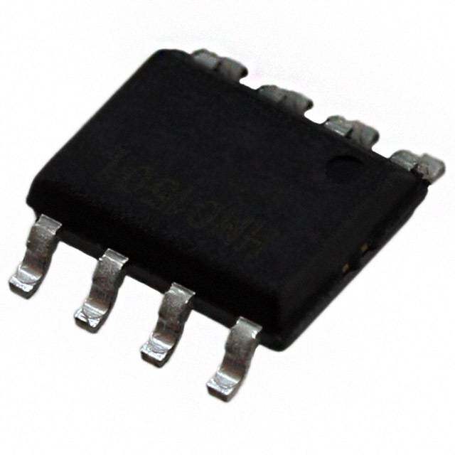
ICGOO电子元器件商城为您提供AS5048B-HTSP-500由AUSTRIAMICROSYSTEMS设计生产,在icgoo商城现货销售,并且可以通过原厂、代理商等渠道进行代购。 AS5048B-HTSP-500价格参考¥33.48-¥101.30。AUSTRIAMICROSYSTEMSAS5048B-HTSP-500封装/规格:位置传感器 - 角,线性位置测量, Hall Effect Sensor Angle External Magnet, Not Included Gull Wing。您可以下载AS5048B-HTSP-500参考资料、Datasheet数据手册功能说明书,资料中有AS5048B-HTSP-500 详细功能的应用电路图电压和使用方法及教程。
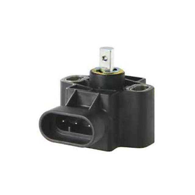
ams(现为艾迈斯半导体)的AS5048B-HTSP-500是一款高精度磁性位置传感器,属于角位置与线性位置测量类别。该传感器基于霍尔效应技术,可实现非接触式绝对角度测量,分辨率高达14位(0.022°),具备出色的重复性和稳定性。

AS5048B-HTSP-500广泛应用于对精度和可靠性要求较高的工业与自动化领域。典型应用场景包括:
- 伺服电机与步进电机反馈系统:用于精确检测电机转子位置,实现闭环控制,提升运动控制精度。
- 机器人关节角度检测:在工业机械臂或协作机器人中,实时监测关节旋转角度,确保动作精准协调。
- 电动助力转向(EPS)系统:应用于汽车或轻型电动车中,检测方向盘转角,提高转向灵敏度与安全性。
- 工业自动化设备:如数控机床、自动装配线中的旋转平台或执行器位置反馈。
- 医疗设备:用于需要精密角度控制的医疗器械,如手术机器人、诊断设备等。

该型号采用SMD封装(HTSP),适合表面贴装工艺,便于集成到紧凑型电子模块中。其内置温度补偿和校准功能,能够在复杂电磁环境和宽温范围内稳定工作。此外,支持SPI和I²C数字输出接口,方便与微控制器通信,简化系统设计。

综上,AS5048B-HTSP-500适用于需高精度、非接触式角度测量的中高端工业、汽车及医疗应用,是现代智能控制系统中的关键传感元件。
| 参数 | 数值 |
| 产品目录 | |
| 描述 | IC ENCODER ROTARY 14-TSSOP板机接口霍耳效应/磁性传感器 14-bit rotary position sensor |
| 产品分类 | 磁性传感器 - 霍尔效应,数字开关,线性,罗盘 (IC)传感器 IC |
| 品牌 | ams |
| 产品手册 | http://ams.com/eng/content/download/250006/975176/143016 |
| 产品图片 |
|
| rohs | 符合RoHS无铅 / 符合限制有害物质指令(RoHS)规范要求 |
| 产品系列 | 板机接口霍耳效应/磁性传感器,ams AS5048B-HTSP-500- |
| 数据手册 | |
| 产品型号 | AS5048B-HTSP-500 |
| 产品 | Magnetic Encoders |
| 产品培训模块 | http://www.digikey.cn/PTM/IndividualPTM.page?site=cn&lang=zhs&ptm=25930 |
| 产品种类 | 板机接口霍耳效应/磁性传感器 |
| 供应商器件封装 | 14-TSSOP |
| 其它名称 | AS5048B-HTSP-500TR |
| 包装 | 带卷 (TR) |
| 参考设计库 | http://www.digikey.com/rdl/4294959886/4294959846/274 |
| 商标 | ams |
| 安装风格 | SMD/SMT |
| 封装 | Reel |
| 封装/外壳 | 14-TSSOP(0.173",4.40mm 宽) |
| 封装/箱体 | TSSOP-14 |
| 工作温度 | -40°C ~ 150°C |
| 工厂包装数量 | 500 |
| 感应范围 | 30mT ~ 70mT |
| 标准包装 | 500 |
| 特性 | 14 位 |
| 特色产品 | http://www.digikey.com/product-highlights/cn/zh/austriamicrosystems-as5048-magnetic-encoder/1804 |
| 电压-电源 | 3.3V,5V |
| 电流-电源 | 15mA |
| 电流-输出(最大值) | 4mA |
| 类型 | 旋转 |
| 输出类型 | PWM |


- 商务部:美国ITC正式对集成电路等产品启动337调查
- 曝三星4nm工艺存在良率问题 高通将骁龙8 Gen1或转产台积电
- 太阳诱电将投资9.5亿元在常州建新厂生产MLCC 预计2023年完工
- 英特尔发布欧洲新工厂建设计划 深化IDM 2.0 战略
- 台积电先进制程称霸业界 有大客户加持明年业绩稳了
- 达到5530亿美元!SIA预计今年全球半导体销售额将创下新高
- 英特尔拟将自动驾驶子公司Mobileye上市 估值或超500亿美元
- 三星加码芯片和SET,合并消费电子和移动部门,撤换高东真等 CEO
- 三星电子宣布重大人事变动 还合并消费电子和移动部门
- 海关总署:前11个月进口集成电路产品价值2.52万亿元 增长14.8%
PDF Datasheet 数据手册内容提取
AS5048A/AS5048B Magnetic Rotary Encoder (14-Bit Angular Position Sensor) General Description The AS5048 is an easy to use 360° angle position sensor with a 14-bit high resolution output. The IC measures the absolute position of the magnet’s rotation angle and consists of Hall sensors, analog digital converter and digital signal processing. The absolute position information of the magnet is directly accessible over a PWM output and can be read out over a standard SPI or a high speed I²C interface. AS5048A has a SPI interface, AS5048B I²C interface. Both devices offer a PWM output. The zero position can be programmed via SPI or I²C command. This simplifies the assembly of the complete system because the zero position of the magnet does not need to be mechanically aligned. The sensor tolerates misalignment, air gap variations, temperature variations and as well external magnetic fields. This robustness and wide temperature range (-40°C up to 150°C) of the AS5048 makes the IC ideal for rotation angle sensing in harsh industrial and medical environments. Several AS5048 ICs can be connected in daisy chain for serial data read out. An internal voltage regulator allows the AS5048 to operate at either 3.3V or 5V supplies. OrderingInformation and ContentGuide appear at end of datasheet. Key Benefits & Features The benefits and features of AS5048A/AS5048B, Magnetic Rotary Encoder (14-Bit Angular Position Sensor) are listed below: Figure 1: Added Value of Using AS5048 Benefits Features • No external programmer needed • Standard SPI or I2C interface and PWM • High precision • 14-bit resolution (0.0219°/LSB) • Easy to use • Zero position programmable via SPI or I2C • Low material costs (no shielding) • Immune to external magnetic stray fields ams Datasheet Page 1 [v1-11] 2018-Jan-29 DocumentFeedback
AS5048A/AS5048B − General Description • Contactless rotary position sensor over 360° • Temperature range: -40°C to 150°C • 3.3V / 5V compliant • Package: 14-pin TSSOP (5 x 6.4mm) Applications The applications of AS5048 include: • Robotic joint position detection • Industrial motor position control • Medical robots and fitness equipment Block Diagram The functional blocks of this device are shown below: Figure 2: AS5048A Block Diagram VDD5V SCK Register VDD3V LDO Setting MISO SPI OTP MOSI CSn 14-bit A/D ATAN AFE 14-bit A/D PWM PWM (CORDIC) AGC AS5048A GND Page 2 ams Datasheet DocumentFeedback [v1-11] 2018-Jan-29
AS5048A/AS5048B − General Description Figure 3: AS5048B Block Diagram VDD5V SCL Register VDD3V LDO Setting SDA I2C OTP A1 A2 AFE 1144--bbiitt AA//DD ATAN PWM PWM (CORDIC) AGC AS5048B GND ams Datasheet Page 3 [v1-11] 2018-Jan-29 DocumentFeedback
AS5048A/AS5048B − Pin Assignments Pin Assignments The AS5048A/AS5048B pin assignments are described below. Figure 4: TSSOP14 Pin Configurations CSn 1 14 PWM SDA 1 14 PWM CLK 2 13 GND SCL 2 13 GND A A MISO 3 S 12 VDD3V A2 3 S 12 VDD3V 5 5 0 0 MOSI 4 4 11 VDD5V A1 4 4 11 VDD5V 8 8 TEST 5 A 10 TEST TEST 5 B 10 TEST TEST 6 9 TEST TEST 6 9 TEST TEST 7 8 TEST TEST 7 8 TEST Figure 5: TSSOP14 Pin Descriptions for AS5048A Pin AS5048A Pin Type Description 1 CSn SPI chip select - active low Digital input with Schmitt trigger 2 CLK SPI clock input Digital I/O with Schmitt 3 MISO SPI master in/slave out trigger in the input path Digital input with Schmitt 4 MOSI SPI master out/slave in trigger 5 TEST Analog I/O Test pin should be connected to GND. 6 TEST 7 TEST Test pins should be left open during normal 8 TEST Analog I/O operation. 9 TEST 10 TEST 11 VDD5V Positive Supply Voltage, 3.0to 5.5 V 3.3V Regulator output; internally regulated from VDD. 12 VDD3V Supply pad Connect to VDD for 3V supply voltage. 10μF capacitor to GND required in 5V operation mode 13 GND Negative Supply Voltage (GND) 14 PWM Digital output – push-pull Pulse Width Modulation output Page 4 ams Datasheet DocumentFeedback [v1-11] 2018-Jan-29
AS5048A/AS5048B − Pin Assignments Figure 6: TSSOP14 Pin Description for AS5048B Pin AS5048B Type Description Digital I/O with open drain 1 SDA Data pin I²C interface output 2 SCL I²C clock input Digital input with Schmitt 3 A2 I²C address selection pin 3 trigger 4 A1 I²C address selection pin 4 5 TEST Analog I/O Test pin should be connected to GND. 6 TEST 7 TEST Test pins should be left open during normal 8 TEST Analog I/O operation. 9 TEST 10 TEST 11 VDD5V Positive Supply Voltage, 3.0to 5.5 V 3.3V Regulator output; internally regulated from VDD. 12 VDD3V Supply pad Connect to VDD for 3V supply voltage. 10μF capacitor to GND required in 5V operation mode 13 GND Negative Supply Voltage (GND) 14 PWM Digital output – push-pull Pulse Width Modulation output ams Datasheet Page 5 [v1-11] 2018-Jan-29 DocumentFeedback
AS5048A/AS5048B − Absolute Maximum Ratings Absolute Maximum Ratings Stresses beyond those listed under Absolute Maximum Ratings may cause permanent damage to the device. These are stress ratings only. Functional operation of the device at these or any other conditions beyond those indicated under Operating Conditions is not implied. Exposure to absolute maximum rating conditions for extended periods may affect device reliability. Figure 7: Absolute Maximum Ratings Symbol Parameter Min Max Unit Note Electrical Parameters VDD5V DC supply voltage at VDD pin -0.3 7 V VDD3V DC voltage at VDD3V pin -0.3 5 V GND DC voltage at GND pin -0.3 0.3 V V Input pin voltage VDD+0.3 V IN I Input current (latchup immunity) -100 100 mA Jedec 78 SCR Electrostatic Discharge ESD Electrostatic discharge ± 2 kV MIL 883 E method 3015 Power Dissipation Total power dissipation P 150 mW T (all supplies and outputs) Temperature Ranges and Storage Conditions T Storage temperature -55 150 °C STRG The reflow peak soldering temperature (body temperature) specified is in accordance with IPC/JEDEC T Package body temperature 260 °C J-STD-020 “Moisture Solid BODY State Surface Mount Devices”. The lead finish from Pb-free leaded packages is matte tin (100%Sn) Relative humidity RH 5 85 % NC non-condensing Represents a maximum floor MSL Moisture sensitivity level 3 life time of 168h Page 6 ams Datasheet DocumentFeedback [v1-11] 2018-Jan-29
AS5048A/AS5048B − Electrical Characteristics Electrical Characteristics All in this specification defined tolerances for external components need to be assured over the whole operation conditions range and also over lifetime. Operating Conditions Figure 8: Operating Conditions Symbol Parameter Min Max Unit Note VDD5V Positive supply voltage 4.5 5.5 V 5V Operation via LDO VDD3V 3 3.6 V LDO output voltage VDDCORE Positive core supply voltage 3 3.6 V Only for 5V operation. T Ambient temperature -40 150 °C AMB T_amb_max for 3V is 125°C I Supply current 15 mA SUP DC/AC Characteristics for Digital Inputs and Outputs Figure 9: DC/AC Characteristics Symbol Parameter Min Max Unit CMOS Digital Input with Schmitt Trigger: CSn, CLK, MOSI and SCL, A1, A2 V High level input voltage 0.7 * VDDCORE V IH V Low level input voltage 0.3 * VDDCORE V IL l Input leakage current 1 μA LEAK CMOS Output: PWM, MISO, SDA V High level output voltage VDDCORE - 0.5 V OH V Low level output voltage GND+0.4 V OL C Capacitive load 50 pF L I Output current 4 mA OUT ams Datasheet Page 7 [v1-11] 2018-Jan-29 DocumentFeedback
AS5048A/AS5048B − Electrical Characteristics Electrical System Specifications VDD5V = 5V, T = -40 to 150°C unless noted otherwise. AMB Figure 10: System Specification Symbol Parameter Conditions Min Typ Max Unit Bz Magnetic input field 30 50 70 mT f Output sampling rate 10.2 11.25 12.4 kHz sample RES Output resolution 14 Bit Noise Sensor output noise 2.73LSB@14bit, rms value 0.06 deg t System propagation delay 90.7 100 110.2 μs prop f PWM frequency 0.907 1 1.102 kHz PWM INL Non-linearity, optimum OPT ± 0.8 deg @25ºC placement of the magnet Non-linearity optimum INL placement of the magnet ±1 deg OPT+TEMP over the full temperature range Non-linearity @ Assuming N35H magnet INL displacement of magnet (D=8mm, H=3mm) 500μm ±1.2 deg DIS+TEMP and temperature -40ºC to displacement in x and y 150ºC z-distance @ 2000μm t Startup time 10 ms startup Page 8 ams Datasheet DocumentFeedback [v1-11] 2018-Jan-29
AS5048A/AS5048B − Functional Description Functional Description The AS5048 is a magnetic Hall sensor system manufactured in a CMOS process. A lateral Hall sensor array is used to measure the magnetic field components perpendicular to the surface of the chip. The AS5048 is uses self-calibration methods to eliminate signal offset and sensitivity drifts. The integrated Hall sensors are placed around the center of the device and deliver a voltage representation of the magnetic flux Bz. Through Sigma-Delta Analog-to-Digital Converter (ADC) and Digital Signal-Processing (DSP) algorithms, the AS5048 provides accurate high-resolution absolute angular position information. This is executed by a Coordinate Rotation Digital Computer (CORDIC) which calculates the angle and the magnitude of the Hall array signals. The DSP is also used to provide digital information at the outputs that indicate movements of the magnet towards or away from the device’s surface, in the z-axis. A small diametrically magnetized (two-pole) standard magnet provides the angular position information. Depending on the system requirements different magnet diameters are possible. Additional flexibility is given by the wide range of the magnetic input range. The AS5048 can be combined with NeFeB, SmCo and alternative magnet materials e.g. hard ferrites. The AS5048 provides a 14-bit binary code representing the angular position of the magnet. The type of output is pre-programmed as SPI version A or I²C version B. Simultaneously a PWM output signal is available in 12 bit format. A simple programming of the zero position is possible over the interface. No additional programmer is needed. The AS5048 uses one time programmable (OTP) fuses for permanent programming of the user settings. The verification is possible over a simple digital readout of the OTP content. ams Datasheet Page 9 [v1-11] 2018-Jan-29 DocumentFeedback
AS5048A/AS5048B − Operation Operation Supply Voltage Configuration The AS5048 operates at 5V ±10%, using an internal Low-Dropout (LDO) voltage regulator. In addition a 3.3V operation is possible. The VDD3V output is intended for internal use only. It must not be loaded with an external load. Figure 11: Connections for 5V and 3.3V Supply Voltages 5V Operation 3.3V Operation 10µF VDD3V VDD3V 100nF 100nF 10µF LDO LDO VDD5V VDD5V Internal Internal VDD3.3V VDD3.3V 4.5 -5.5V 3.0-3.6V GND GND Note(s): 1. The pin VDD3V must always be buffered by a 10 μF capacitor in 5V operation. It must not be left floating, as this may cause unstable internal supply voltages which may lead to larger output jitter of the measured angle. In 3V operation the VDD3V must be shorted to VDD5V. The ambient temperature T is limited to 125°C in this mode. AMB SPI Interface The 16 bit SPI Interface enables read / write access to the register blocks and is compatible to a standard micro controller interface. The SPI is active as soon as CSn is pulled low. The AS5048A then reads the digital value on the MOSI (master out slave in) input with every falling edge of CLK and writes on its MISO (master in slave out) output with the rising edge. After 16 clock cycles CSn has to be set back to a high status in order to reset some parts of the interface core. SPI Interface Signals (4-Wire Mode, Wire_mode = 1) The AS5048A only supports slave operation mode. Therefore CLK for the communication as well as the CSn signal has to be provided by the test equipment. The following picture shows a basic interconnection diagram with one master and an AS5048A device and a principle schematic of the interface core. Page 10 ams Datasheet DocumentFeedback [v1-11] 2018-Jan-29
AS5048A/AS5048B − Operation Figure 12: SPI Connection AS5048A with μC CLK SPI_CLK CSn SPI_SS N MOSI MOSI Interface Core RXSR Master Device RXSPI (Tester) TXSPI TXSR MISO MISO AS5048A Because the interface has to decode the sent command before it can react and provide data the response of the chip to a specific command applied at a time T can be accessed in the next transmission cycle ending at T + TCOM. The data are sent and read with MSB first. Every time the chip is accessed it is sending and receiving data. Figure 13: SPI Command/Response Data Flow T COM MSB LSB MSB LSB MSB LSB MSB LSB MOSI Command 1 Command 2 Command 3 Command N MISO NOP Response 1 Response 2 Response N-1 MSB LSB MSB LSB MSB LSB MSB LSB Transmission 1 Transmission 2 Transmission 3 Transmission N ams Datasheet Page 11 [v1-11] 2018-Jan-29 DocumentFeedback
AS5048A/AS5048B − Operation SPI Timing Figure 14: SPI Timing Diagram t CSn CSn (Input) t t t t t L clk clkL clkH H CLK (Input) t t MISO OZ MISO data[15] data[14] data[0] (Output) t OZ t MOSI MOSI data[15] data[14] data[0] (Input) Figure 15: SPI Timing Characteristics Parameter Description Min Max Unit t Time between CSn falling edge and CLK rising edge 350 ns L T Serial clock period 100 ns CLK t Low period of serial clock 50 ns CLKL t High period of serial clock 50 ns CLKH t Time between last falling edge of CLK and rising edge of CSn 50 ns H T High time of CSn between two transmissions 350 ns CSnH t Data input valid to clock edge 20 ns MOSI t CLK edge to data output valid 20 ns MISO Page 12 ams Datasheet DocumentFeedback [v1-11] 2018-Jan-29
AS5048A/AS5048B − Operation SPI Connection to the Host μC Single Slave Mode Figure 16: Single Slave Mode 4 wire mode MOSI 0xFFFF 0xFFFF 0xFFFF 0xFFFF MOSI MOSI Read angle 1 Read angle 2 Read angle 3 Read angle 4 MISO MISO µC AS5048A MISO Angle 1 Angle 2 Angle 3 SCK SCK SS/ SS/ SS/ 3 wire mode (Read only) MISO Angle 1 Angle 2 Angle 3 MOSI 1 MOSI MISO MISO µC AS5048A SS/ SCK SCK SS/ SS/ Single Slave Mode: This figure shows the SPI connection to the host μC using Single Slave Mode. 3 Wire Mode (read only) Figure 17: Multiple Slave, n+3 Wire (Separate ChipSelect) MOSI MOSI MISO MISO MOSI SW Reset Rea0dx FaFnFgFle 1 Rea0dx FaFnFgFle 2 Rea0dx FaFnFgFle 3 AS5048A SCK SCK µC 1 MISO Angle 1 Angle 2 Angle 3 SS1/ SS/ SS2/ SS1/ SS3/ SS2/ MOSI MISO SS3/ AS5048A SCK 2 SS/ MOSI MISO AS5048A SCK 3 SS/ Multiple Slave, n+3 Wire (Separate ChipSelect): This figure shows the SPI connection to the host μC using 3 Wire mode. ams Datasheet Page 13 [v1-11] 2018-Jan-29 DocumentFeedback
AS5048A/AS5048B − Operation Daisy Chain, 4 Wire Figure 18: Daisy Chain, 4 Wire MOSI SW Reset SW Reset SW Reset MOSI MOSI MISO MISO AS5048A µC 1 MISO SCK SCK SS/ SS/ SS/ MOSI MISO AS5048A MOSI Rea0dx FAFnFgFle 3 Rea0dx FaFnFgFle 2 Rea0dx FAFnFgFle 1 Rea0dx FaFnFgFle 3 Rea0dx FaFnFgFle 2 Rea0dx FaFnFgFle 1 2 SCK SS/ MISO Angle 3 Angle 2 Angle 1 SS/ MOSI MISO AS5048A SCK 3 SS/ Daisy Chain, 4 Wire: This figure shows the SPI connection to the host μC using Daisy Chain, 4 wire mode. SPI Communication Command Package Every command sent to the AS5048A is represented with the following layout. Figure 19: SPI Command Package Command Package Bit MSB 14 13 12 11 10 9 8 7 6 5 4 3 2 1 LSB PAR RWn Address<13:0> Bit Definition & Description PAR Parity bit (EVEN) RWn Indicates read(1) or write(0) command Address 14 bit address code Page 14 ams Datasheet DocumentFeedback [v1-11] 2018-Jan-29
AS5048A/AS5048B − Operation Read Package (Value Read from AS5048A) The read frame always contains two alarm bits, the parity and error flags and the addressed data of the previous read command. Figure 20: SPI Read Package Read Package Bit MSB 14 13 12 11 10 9 8 7 6 5 4 3 2 1 LSB PAR EF Data<13:0> Bit Definition & Description PAR Parity bit (EVEN) EF Error flag indicating a transmission error in a previous host transmission Data 14 bit addressed data Write Data Package (Value Written to AS5048A) The write frame is compatible to the read frame and contains two additional bits, parity flag and R flag. If the previous command was a write command a second package has to be transmitted. Figure 21: SPI Write Data Package Data Package Bit MSB 14 13 12 11 10 9 8 7 6 5 4 3 2 1 LSB PAR R Data <13:0> Bit Definition & Description PAR Parity bit (EVEN) R Has to be 0 Data 14 bit data to write to former selected address ams Datasheet Page 15 [v1-11] 2018-Jan-29 DocumentFeedback
AS5048A/AS5048B − Register Description Register Description Figure 22: SPI Register Map Address Access Name Bit Symbol Default Description hex Type Control and Error Registers 13 No operation dummy x0000 NOP R : NOP 0 information 0 13 : Not used n.a. 3 Clear Error Error register. All errors x0001 R Flag are cleared by access 2 Parity Error 1 Command Invalid 0 0 Framing Error 13 : Not used 7 Programming control 6 Verify register. Programming must be 5 enabled before burning Programming Not used x0003 R/W 0 the fuse(s). After Control 4 programming is a 3 Burn verification mandatory. See programming 2 procedure. Reserved 1 Programming 0 Enable Page 16 ams Datasheet DocumentFeedback [v1-11] 2018-Jan-29
AS5048A/AS5048B − Register Description Address Access Name Bit Symbol Default Description hex Type Programmable Customer Settings 13 : Not used 0 OTP Register R/W 8 Zero Position value high x0016 Zero Position + byte Hi Program 7 Zero Position <13> 0 : : : 0 Zero Position <6> 0 13 : Not used 0 OTP Register R/W 6 Zero Position remaining x0017 Zero Position + 6 lower LSB's Low 6 LSBs Program 5 Zero Position <5> 0 : : : 0 Zero Position <0> 0 Readout Registers 13 Not used n.a. 12 11 Comp High 0 Diagnostics flags 10 Comp Low 0 Diagnostics + Automatic 9 COF 0 x3FFD R Gain Control 8 OCF 1 (AGC) 7 AGC value<7> 1 Automatic Gain Control value. : : : 0 decimal represents high magnetic field, 255 decimal represents low 0 AGC value<0> 0 magnetic field 13 Magnitude<13> 0 Magnitude output value x3FFE Magnitude R : : : of the CORDIC 0 Magnitude<0> 0 13 Angle <13> 0 Angle output value x3FFF Angle R : : : including zero position correction 0 Angle<0> 0 ams Datasheet Page 17 [v1-11] 2018-Jan-29 DocumentFeedback
AS5048A/AS5048B − SPI Interface Commands SPI Interface Commands READ Command For a single READ command two transmission sequences are necessary. The first package written to the AS5048 contains the READ command (MSB-1 high) and the address the chip has to access, the second package transmitted to the AS5048 device can be any command the chip has to process next. The content of the desired register is available in the MISO register of the master device at the end of the second transmission cycle. Figure 23: READ Command T COM MSB LSB MSB LSB MOSI READ Next command MISO Response on Response -1 READ command MSB LSB MSB LSB Transmission N Transmission N+1 WRITE Command A single WRITE command takes two transmission cycles. With a NOP command after the WRITE command you can verify the sent data with three transmission cycles because the data will be send back during the following command. Figure 24: WRITE Command T COM MSB LSB MSB LSB MSB LSB MOSI WRITE DATA NOP command MISO Old register New register Response-1 content content MSB LSB MSB LSB MSB LSB Transmission N Transmission N+1 Transmission N+2 Page 18 ams Datasheet DocumentFeedback [v1-11] 2018-Jan-29
AS5048A/AS5048B − SPI Interface Commands CLEAR ERROR FLAG Command The CLEAR ERROR FLAG command is implemented as READ command. This command clears the ERROR FLAG which is contained in every READ frame. Before the ERROR FLAG is cleared the error register content comes back with the information which error type was occurred. On the next new READ register the ERROR FLAG is cleared. Figure 25: CLEAR ERROR FLAG Command T COM MSB LSB MSB LSB MOSI CLEAR ERROR Next command Next command FLAG MISO Response-1 Error register New register EF Content + EF EF cleared MSB LSB MSB LSB MSB LSB Transmission N Transmission N+1 Transmission N+2 The package necessary to perform a CLEAR ERROR FLAG is built up as follows. Figure 26: Clear Error Flag Command CLEAR ERROR FLAG Command Bit MSB 14 13 12 11 10 9 8 7 6 5 4 3 2 1 LSB PAR 1 0 0 0 0 0 0 0 0 0 0 0 0 0 1 Possible conditions which force the ERROR FLAG to be set: • Wrong parity • Wrong number of clocks (no full transmission cycle or too many clocks) • Invalid command • Frame error Note(s): If the error flag is set to high because of a communication problem the flag remains set until it will be cleared by the CLERAR ERROR FLAG command. ams Datasheet Page 19 [v1-11] 2018-Jan-29 DocumentFeedback
AS5048A/AS5048B − SPI Interface Commands NOP Command The NOP command represents a dummy write to the AS5048. Figure 27: NOP Command T COM MSB LSB MSB LSB MSB LSB MOSI NOP NOP Next command MISO Response-1 0x0000 0x0000 MSB LSB MSB LSB MSB LSB Transmission N Transmission N+1 Transmission N+2 The NOP command frame looks like follows. Figure 28: NOP Command NOP Command Bit MSB 14 13 12 11 10 9 8 7 6 5 4 3 2 1 LSB 0 0 0 0 0 0 0 0 0 0 0 0 0 0 0 0 The chip’s response on this command is 0x0000 Page 20 ams Datasheet DocumentFeedback [v1-11] 2018-Jan-29
AS5048A/AS5048B − I²C Interface I²C Interface The AS5048B supports 2-wire high-speed I²C protocol in device mode. The host MCU (master) has to initiate the data transfers. The 7-bit device address of the slave depends on the state of the OTP I²C register 21 (0x15) bit 0… 4 + 2 I²C address selection pin 3 and 4. Supported modes: • Random/Sequential Read • Byte/Page Write • Standard : 0 to 100kHz clock frequency (slave mode) • Fast Mode : 0 to 400kHz clock frequency (slave mode) • High Speed: 0 to 3.4MHz clock frequency (slave mode) The SDA signal is bidirectional and is used to read and write the serial data. The SCL signal is the clock generated by the host MCU, to synchronize the SDA data in read and write mode. The maximum I²C clock frequency is 3.4MHz, data are triggered on the rising edge of SCL. I²C Electrical Specification Figure 29: I²C Electrical Specification HS-mode HS-mode FS-mode+ C =100pF C =400pF Symbol Parameter Condition B B Unit Min Max Min Max Min Max LOW-Level Input 0.3V 0.3V 0.3V VIL Voltage -0.5 ORDEDC -0.5 ORDEDC -0.5 ORDEDC V VIH HVoIGltHag-Leevel Input 0.C7OVRDED VD+D 0C.O5R E 0.C7OVRDED VD+D 0C.O5R E 0.C7OVRDED VD+D 0C.O5R E V Hysteresis of Schmitt 0.1V 0.1V 0.1V Vhys Trigger Inputs VDDCORE< 2V CORDED -- CORDED -- CORDED -- V LOW-Level Output Voltage (open-drain 0.2V 0.2V 0.2V VOL or open-collector) at VDDCORE< 2V -- ORDEDC -- ORDEDC -- ORDEDC V 3mA Sink Current LOW-Level Output IOL Current VOL = 0.4V 20 -- -- -- -- mA Pull-up current of ICS SCLH current source -- -- 3 12 3 12 mA Pulse Width of Spikes that must be tSP suppressed by the -- 50 (1) -- 10 -- 10 ns Input Filter ams Datasheet Page 21 [v1-11] 2018-Jan-29 DocumentFeedback
AS5048A/AS5048B − I²C Interface HS-mode HS-mode FS-mode+ C =100pF C =400pF Symbol Parameter Condition B B Unit Min Max Min Max Min Max Input Input Current at each Ii I/O Pin Voltage -10 +10 (2) -- 10 -- 10 μA between Total Capacitive Load CB for each Bus Line -- 550 -- 100 -- 400 pF I/O Capacitance CI/O (SDA,SCL) -- 10 -- 10 -- 10 pF Note(s): 1. Input filters on the SDA and SCL inputs suppress noise spikes of less than 50 ns. 2. I/O pins of Fast-mode and Fast-mode Plus devices must not obstruct the SDA and SCL lines if VDD is switched OFF. I²C Timing Figure 30: I²C Timing HS-mode HS-mode FS-mode C =100pF C =400pF (5) B B Symbol Parameter Condition Unit Min Max Min Max Min Max SCL clock f -- 400 -- 3400 -- 1700 kHz SCLK Frequency Bus Free Time; time t between STOP and 500 -- 500 -- 500 -- ns BUF START Condition Hold Time; t (Repeated) START 260 -- 160 -- 160 -- ns HD;STA Condition (1) LOW Period of SCL t 500 -- 160 -- 320 -- ns LOW Clock HIGH Period of SCL t 260 -- 60 -- 120 -- ns HIGH Clock Setup Time for a t Repeated START 260 -- 160 -- 160 -- ns SU;STA condition tHD;DAT Data Hold Time (2) 0 450 0 70 0 150 ns tSU;DAT Data Setup Time (3) 50 -- 10 -- 10 -- ns Rise Time of SDA t 20+0.1C 120 -- -- -- -- ns R and SCL Signals b Page 22 ams Datasheet DocumentFeedback [v1-11] 2018-Jan-29
AS5048A/AS5048B − I²C Interface HS-mode HS-mode FS-mode C =100pF C =400pF (5) Symbol Parameter Condition B B Unit Min Max Min Max Min Max Fall time of SDA and tF SCL signals 20+0.1Cb 120 (4) -- -- -- -- ns Ext. pull-up Rise time of SCLH t source of -- -- 10 40 20 80 ns rCL signal 3mA Rise time of SCLH signal after Ext. pull-up t repeated START source of -- -- 10 80 20 160 ns rCL1 condition and after 3mA an acknowledge bit Ext. pull-up Output rise time of t source of -- -- 10 40 20 80 ns fCL SCLH signal 3mA Output rise time of t -- -- 10 80 20 160 ns rDA SDAH signal Output rise time of t -- -- 10 80 20 160 ns fDA SDAH signal Setup Time for t 260 -- 160 -- 160 -- ns SU;STO STOP Condition Noise margin at V 0.1V -- 0.1V -- 0.1V -- V nL LOW level DDp DDp DDp Noise margin at V 0.2V -- 0.2V -- 0.2V -- V nH HIGH level DDp DDp DDp Note(s): 1. After this time the first clock is generated. 2. A device must internally provide a minimum hold time (120ns / max 250ns for Fast-mode Plus, 80ns / max 150ns for High-speed mode) for the SDA signal (referred to the V of the SCL) to bridge the undefined region of the falling edge of SCL. IHmin 3. A fast-mode device can be used in standard-mode system, but the requirement t = 250ns must then e met. This is automatically SU;DAT the case if the device does not stretch the LOW period of the SCL signal. If such a device does stretch the LOW period of the SCL signal, it must output the next data bit to the SDA line t + T = 1000 + 250 = 1250ns before the SCL line is released. Rmax SU;DAT 4. In Fast-mode Plus, fall time is specified the same for both output stage and bus timing. If series resistors are used this has to be considered for bus timing. 5. For capacitive bus loads between 100pF and 400pF, the timing parameters must be linearly interpolated ams Datasheet Page 23 [v1-11] 2018-Jan-29 DocumentFeedback
AS5048A/AS5048B − I²C Interface Register Table The following registers / functions are accessible over the serial I²C interface. Figure 31: Register Map I²C Address Access Name Bit Symbol Default Description hex Type Control OTP 7 Not used 6 Verify 5 Programming control Not used register. Programming 4 must be enabled before Programming burning the fuse(s). After x03 R/W 0 Control 3 Burn programming is an verification mandatory. 2 See programming Reserved procedure. 1 Programming 0 Enable Programmable Customer Settings 7 : Not used n.a. I²C slave address slave 5 address consist of 5 bits I²C slave (MSBs) and the hardware x15 R/W address internally setting of Pins A1 andA2 4 I²C address<4> inverted I²C address <4> is the inversion defined as '1' : : : 0 I²C address<0> 0 7 Zero Position <13> 0 OTP Register R/W Zero Position value high x16 Zero Position + : : : byte Hi Program 0 Zero Position <6> 0 7 Not used n.a. 6 OTP Register R/W Zero Position remaining x17 Zero Position + 5 Zero Position <5> 0 6 lower LSB's Low 6 LSBs Program : : : 0 Zero Position <0> 0 Page 24 ams Datasheet DocumentFeedback [v1-11] 2018-Jan-29
AS5048A/AS5048B − I²C Interface Address Access Name Bit Symbol Default Description hex Type Readout Registers 7 AGC value<7> 1 Automatic Gain Control value. Automatic : : : 0 decimal represents xFA Gain R high magnetic field 255 Control decimal represents low 0 AGC value<0> 0 magnetic field 7 : Not used n.a. 4 xFB Diagnostics R 3 Comp High 0 Diagnostic flags 2 Comp Low 0 1 COF 0 0 OCF 1 7 Magnitude<13> 0 xFC R : : : 0 Magnitude<6> 0 7 Magnitude output value Magnitude Not used n.a. of the CORDIC 6 xFD R 5 Magnitude<5> 0 : : : 0 Magnitude<0> 0 7 Angle<13> 0 xFE R : : : 0 Angle<6> 0 7 Angle output value Angle Not used n.a. including zero position 6 correction xFF R 5 Angle<5> 0 : : : 0 Angle<0> 0 ams Datasheet Page 25 [v1-11] 2018-Jan-29 DocumentFeedback
AS5048A/AS5048B − I²C Interface I²C Slave address Figure 32: Slave Address Construction OTP cotent HW HW K (Default) Pins Pins AC random read A A A A 1 0 0 0 0 X X X X X X X X 1 0 0 0 0 X X X X X X X X 2 1 2 1 Start Slave Address R/WACK Register Address ACK Start Slave Address R/WACK Data Byte (n) Stop B B S S L L OTP cotent HW (Default) Pins random write A A 1 0 0 0 0 X X X X X X X X X X X X X X X X 2 1 Start Slave Address R/WACK Register Address ACK Data Byte (n) ACK Stop B S L Note(s): 1. It's important to use a STOP condition only after a complete read or write sequence. The slave address consists of the hardware setting on pins A1, A2. The MSB of the slave address (yellow) is internally inverted. This means that by default the resulting data is ‘1’. A read of the I²C slave address register 21 will return a ‘0’ at the MSB. Page 26 ams Datasheet DocumentFeedback [v1-11] 2018-Jan-29
AS5048A/AS5048B − PWM Interface PWM Interface The AS5048 provides a pulse width modulated output (PWM), whose duty cycle is proportional to the measured angle. The PWM frequency is internally trimmed to an accuracy of ±10% over full temperature range. This tolerance can be cancelled by measuring the complete duty cycle. The PWM signal consists of different sections: • Init: 12 clocks → PWM = ‘high’ • Error_n: 4 clocks → PWM = ‘not(system_error)’ • Data: 4095 clocks → PWM = ‘angle_zero’ / ‘low’ (in case of error) • Exit: 8 clocks → PWM = ‘low’ In case of an error the data section is set to zero. Figure 33: PWM Format Init Error_n Zero degree Data Exit 16 clocks 4095 clocks 8 clocks Figure 34: PWM Period and Resolution Parameter Symbol Value Unit PWM Frequency F_PWM 1 KHz PWM Pulse period T_PWM 4119 bit ams Datasheet Page 27 [v1-11] 2018-Jan-29 DocumentFeedback
AS5048A/AS5048B − Application Information Application Information Programming of the AS5048 Programming of the Zero Position: The absolute angle position can be permanent programmed over the interface. This could be useful for random placement of the magnet on the rotation axis. A readout at the mechanical zero position can be performed and written back into the IC. With permanent programming the position is non-reversible stored in the IC. This programming can be performed only once. To simplify the calculation of the zero position it is only needed to write the value in the IC which was read out before from the angle register. Programming Sequence with Verification: To program the zero position is needed to perform following sequence: 1. Write 0 into OTP zero position register to clear 2. Read angle information 3. Write previous read angle position into OTP zero position register Now the zero position is set. If you want to burn it to the OTP register send: 4. Set the Programming Enable bit in the OTP control register 5. Set the Burn bit to start the automatic programming procedure 6. Read angle information (equals to 0) 7. Set the Verify bit to load the OTP data again into the internal registers 8. Read angle information (equals to 0) The programming can either be performed in 5V operation using the internal LDO, or in 3V operation but using a minimum supply voltage of 3.3V. In case of 3V operation, also a 10μF capacitor is required on the VDD3 pin. Programming the I²C Slave address: For informations of programming the I²C Slave address please refer to our application note covering this topic. Page 28 ams Datasheet DocumentFeedback [v1-11] 2018-Jan-29
AS5048A/AS5048B − Application Information Diagnostic Functions of the AS5048 The AS5048 provides diagnostics functions of the IC and also diagnostic functions of the magnetic input field Following diagnostic flags are available: See Figure22 register address x3FFD (AS5048A) or Figure31 register address 251 dec (AS5048B) • OCF (Offset Compensation Finished), logic high indicates the finished Offset Compensation Algorithm. After power up the flag remains always to logic high. • COF (CORDIC Overflow), logic high indicates an out of range error in the CORDIC part. When this bit is set, the angle and magnitude data is invalid. The absolute output maintains the last valid angular value. • COMP low, indicates a high magnetic field. It is recommended to monitor in addition the magnitude value. • COMP high, indicated a weak magnetic field. It is recommended to monitor the magnitude value. ams Datasheet Page 29 [v1-11] 2018-Jan-29 DocumentFeedback
AS5048A/AS5048B − Application Information Choosing the Proper Magnet The AS5048 works with a variety of different magnets in size and shape. Atypical magnet could be 6-8 mm in diameter and ≥2.5mm in height The magnetic field strength perpendicular to the die surface has to be in the range of ±30mT … ±70mT (peak). The magnet’s field strength should be verified using a gauss-meter. The magnetic flux B at a given distance, along a Z concentric circle with a radius of 1.1mm (R1), should be in the range of ±30mT… ±70mT. Figure 35: Typical Magnet and Magnetic Flux Distribution typ. 6-8mm diameter N S Magnet axis Magnet axis R1 Vertical field component N S R1 concentric circle; radius 1.1mm Vertical field component Bv (30…70mT) 0 360 Page 30 ams Datasheet DocumentFeedback [v1-11] 2018-Jan-29
AS5048A/AS5048B − Application Information Physical Placement of the Magnet The best linearity can be achieved by placing the center of the magnet exactly over the defined center of the chip as shown in the drawing below: Figure 36: Defined Chip Center and Magnet Displacement Radius 3.2mm 3.2mm 1 2.5mm Defined center R d 2.5mm Area of recommended maximum magnet misalignment Magnet Placement The magnet’s center axis should be aligned within a displacement radius R of 0.25 mm (larger magnets allow more d displacement e.g. 0.5 mm) from the defined center of the IC. The magnet may be placed below or above the device. The distance should be chosen such that the magnetic field on the die surface is within the specified limits The typical distance “z” between the magnet and the package surface is 0.5mm to 2.5mm, provided the use of the recommended magnet material and dimensions (6mm x 3mm). Larger distances are possible, as long as the required magnetic field strength stays within the defined limits. However, a magnetic field outside the specified range may still produce usable results, but the out-of-range condition will be indicated by indication flags. Figure 37: Vertical Placement of the Magnet S N Package surface Die surface ams Datasheet Page 31 [v1-11] 2018-Jan-29 DocumentFeedback
AS5048A/AS5048B − Application Information Mechanical Data The internal Hall elements are placed in the center of the package on a circle with a radius of 1.1 mm. Figure 38: Hall Element Positions Note(s): 1. All dimensions in mm. 2. Die thickness 203μm nom. 3. Adhesive thickness 30 ± 15μm. 4. Leadframe downset 152 ± 25 μm. 5. Leadframe thickness 125 ± 8 μm. Page 32 ams Datasheet DocumentFeedback [v1-11] 2018-Jan-29
AS5048A/AS5048B − Package Drawings & Markings Package Drawings & Markings Package type: TSSOP14 Figure 39: Package Markings for AS5048A & AS5048B Figure 40: Package Code YYWWMZZ YY WW M ZZ Last two digits of the Manufacturing week Plant identifier Letters for free traceability manufacturing year ams Datasheet Page 33 [v1-11] 2018-Jan-29 DocumentFeedback
AS5048A/AS5048B − Package Drawings & Markings Figure 41: 14-Lead Thin Shrink Small Outline Package TSSOP-14 RoHS Green Symbol Min Nom Max Symbol Min Nom Max A - - 1.20 R 0.09 - - A1 0.05 - 0.15 R1 0.09 - - A2 0.80 1.00 1.05 S 0.20 - - b 0.19 - 0.30 θ1 0º - 8º c 0.09 - 0.20 θ2 - 12 REF - D 4.90 5.00 5.10 θ3 - 12 REF - E - 6.40 BSC - aaa - 0.10 - E1 4.30 4.40 4.50 bbb - 0.10 - e - 0.65 BSC - ccc - 0.05 - L 0.45 0.60 0.75 ddd - 0.20 - L1 - 1.00 REF - N 14 Note(s): 1. Dimensioning & toleranceing confirm to ASME Y14.5M-1994. 2. All dimensions are in millimeters. Angles are in degrees. Page 34 ams Datasheet DocumentFeedback [v1-11] 2018-Jan-29
AS5048A/AS5048B − Ordering & Contact Information Ordering & Contact Information The devices are available as standard products. Figure 42: Ordering Information Ordering Code Package Description Delivery Form 14 –Bit Programmable Magnetic Rotary Encoder AS5048A-HTSP TSSOP 14 Tape & Reel with SPI-Interface 14 –Bit Programmable Magnetic Rotary Encoder AS5048B-HTSP TSSOP 14 Tape & Reel with I²C-Interface Buy our products or get free samples online at: www.ams.com/ICdirect Technical Support is available at: www.ams.com/Technical-Support Provide feedback about this document at: www.ams.com/Document-Feedback For further information and requests, e-mail us at: ams_sales@ams.com For sales offices, distributors and representatives, please visit: www.ams.com/contact Headquarters ams AG Tobelbader Strasse 30 8141 Premstaetten Austria, Europe Tel: +43 (0) 3136 500 0 Website: www.ams.com ams Datasheet Page 35 [v1-11] 2018-Jan-29 DocumentFeedback
AS5048A/AS5048B − RoHS Compliant & ams Green Statement RoHS Compliant & ams Green RoHS: The term RoHS compliant means that ams AG products fully comply with current RoHS directives. Our semiconductor Statement products do not contain any chemicals for all 6 substance categories, including the requirement that lead not exceed 0.1% by weight in homogeneous materials. Where designed to be soldered at high temperatures, RoHS compliant products are suitable for use in specified lead-free processes. ams Green (RoHS compliant and no Sb/Br): ams Green defines that in addition to RoHS compliance, our products are free of Bromine (Br) and Antimony (Sb) based flame retardants (Br or Sb do not exceed 0.1% by weight in homogeneous material). Important Information: The information provided in this statement represents ams AG knowledge and belief as of the date that it is provided. ams AG bases its knowledge and belief on information provided by third parties, and makes no representation or warranty as to the accuracy of such information. Efforts are underway to better integrate information from third parties. ams AG has taken and continues to take reasonable steps to provide representative and accurate information but may not have conducted destructive testing or chemical analysis on incoming materials and chemicals. ams AG and ams AG suppliers consider certain information to be proprietary, and thus CAS numbers and other limited information may not be available for release. Page 36 ams Datasheet DocumentFeedback [v1-11] 2018-Jan-29
AS5048A/AS5048B − Copyrights & Disclaimer Copyrights & Disclaimer Copyright ams AG, Tobelbader Strasse 30, 8141 Premstaetten, Austria-Europe. Trademarks Registered. All rights reserved. The material herein may not be reproduced, adapted, merged, translated, stored, or used without the prior written consent of the copyright owner. Devices sold by ams AG are covered by the warranty and patent indemnification provisions appearing in its General Terms of Trade. ams AG makes no warranty, express, statutory, implied, or by description regarding the information set forth herein. ams AG reserves the right to change specifications and prices at any time and without notice. Therefore, prior to designing this product into a system, it is necessary to check with ams AG for current information. This product is intended for use in commercial applications. Applications requiring extended temperature range, unusual environmental requirements, or high reliability applications, such as military, medical life-support or life-sustaining equipment are specifically not recommended without additional processing by ams AG for each application. This product is provided by ams AG “AS IS” and any express or implied warranties, including, but not limited to the implied warranties of merchantability and fitness for a particular purpose are disclaimed. ams AG shall not be liable to recipient or any third party for any damages, including but not limited to personal injury, property damage, loss of profits, loss of use, interruption of business or indirect, special, incidental or consequential damages, of any kind, in connection with or arising out of the furnishing, performance or use of the technical data herein. No obligation or liability to recipient or any third party shall arise or flow out of ams AG rendering of technical or other services. ams Datasheet Page 37 [v1-11] 2018-Jan-29 DocumentFeedback
AS5048A/AS5048B − Document Status Document Status Document Status Product Status Definition Information in this datasheet is based on product ideas in the planning phase of development. All specifications are Product Preview Pre-Development design goals without any warranty and are subject to change without notice Information in this datasheet is based on products in the design, validation or qualification phase of development. Preliminary Datasheet Pre-Production The performance and parameters shown in this document are preliminary without any warranty and are subject to change without notice Information in this datasheet is based on products in ramp-up to full production or full production which Datasheet Production conform to specifications in accordance with the terms of ams AG standard warranty as given in the General Terms of Trade Information in this datasheet is based on products which conform to specifications in accordance with the terms of Datasheet (discontinued) Discontinued ams AG standard warranty as given in the General Terms of Trade, but these products have been superseded and should not be used for new designs Page 38 ams Datasheet DocumentFeedback [v1-11] 2018-Jan-29
AS5048A/AS5048B − Revision Information Revision Information Changes from 1-09 (2016-Nov-15) to current revision 1-11 (2018-Jan-29) Page 1-09 (2016-Nov-15) to 1-10 (2018-Jan-25) Updated Figure 5 4 1-10 (2018-Jan-25) to 1-11 (2018-Jan-29) Updated Figure 6 5 Note(s): 1. Page and figure numbers for the previous version may differ from page and figure numbers in the current revision. 2. Correction of typographical errors is not explicitly mentioned. ams Datasheet Page 39 [v1-11] 2018-Jan-29 DocumentFeedback
AS5048A/AS5048B − Content Guide Content Guide 1 General Description 1 Key Benefits & Features 2 Applications 2 Block Diagram 4 Pin Assignments 6 Absolute Maximum Ratings 7 Electrical Characteristics 7 Operating Conditions 7 DC/AC Characteristics for Digital Inputs and Outputs 8 Electrical System Specifications 9 Functional Description 10 Operation 10 Supply Voltage Configuration 10 SPI Interface 10 SPI Interface Signals (4-Wire Mode, Wire_mode = 1) 12 SPI Timing 13 SPI Connection to the Host μC 13 Single Slave Mode 13 3 Wire Mode (read only) 14 Daisy Chain, 4 Wire 14 SPI Communication Command Package 15 Read Package (Value Read from AS5048A) 15 Write Data Package (Value Written to AS5048A) 16 Register Description 18 SPI Interface Commands 18 READ Command 18 WRITE Command 19 CLEAR ERROR FLAG Command 20 NOP Command 21 I²C Interface 21 I²C Electrical Specification 22 I²C Timing 24 Register Table 26 I²C Slave address 27 PWM Interface Page 40 ams Datasheet DocumentFeedback [v1-11] 2018-Jan-29
AS5048A/AS5048B − Content Guide 28 Application Information 28 Programming of the AS5048 29 Diagnostic Functions of the AS5048 30 Choosing the Proper Magnet 31 Physical Placement of the Magnet 31 Magnet Placement 32 Mechanical Data 33 Package Drawings & Markings 35 Ordering & Contact Information 36 RoHS Compliant & ams Green Statement 37 Copyrights & Disclaimer 38 Document Status 39 Revision Information ams Datasheet Page 41 [v1-11] 2018-Jan-29 DocumentFeedback
Mouser Electronics Authorized Distributor Click to View Pricing, Inventory, Delivery & Lifecycle Information: a ms: AS5048A-HTSP-500 AS5048B-HTSP-500