 Datasheet下载
- 型号: JS28F256M29EWHA
- 制造商: Micron Technology Inc
- 库位|库存: xxxx|xxxx
- 要求:
| 数量阶梯 | 香港交货 | 国内含税 |
| +xxxx | $xxxx | ¥xxxx |
查看当月历史价格
查看今年历史价格
JS28F256M29EWHA产品简介:
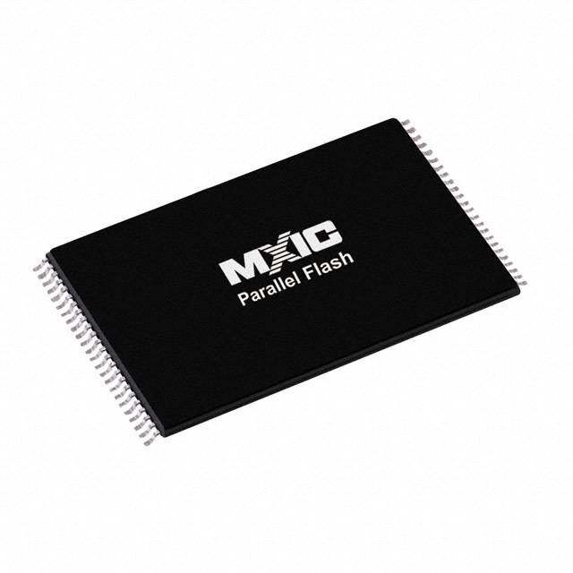
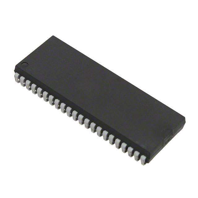
ICGOO电子元器件商城为您提供JS28F256M29EWHA由Micron Technology Inc设计生产,在icgoo商城现货销售,并且可以通过原厂、代理商等渠道进行代购。 JS28F256M29EWHA价格参考。Micron Technology IncJS28F256M29EWHA封装/规格:存储器, FLASH - NOR 存储器 IC 256Mb (32M x 8,16M x 16) 并联 110ns 56-TSOP(14x20)。您可以下载JS28F256M29EWHA参考资料、Datasheet数据手册功能说明书,资料中有JS28F256M29EWHA 详细功能的应用电路图电压和使用方法及教程。
Micron Technology Inc.(美光科技)生产的存储器型号 JS28F256M29EWHA 属于一种闪存(Flash Memory)芯片,具体为 NOR Flash 类型。以下是该型号的应用场景分析:

 1. 嵌入式系统
   - 应用场景:工业控制、家用电器、汽车电子、消费类电子产品等。
   - 特点:NOR Flash 具有随机访问和快速读取能力,适合用于存储嵌入式系统的启动代码(Boot Code)和固件(Firmware)。JS28F256M29EWHA 提供大容量存储空间(256Mb),能够满足复杂嵌入式设备的需求。

 2. 网络通信设备
   - 应用场景:路由器、交换机、调制解调器等。
   - 特点:在网络设备中,NOR Flash 通常用于存储设备的引导程序(Bootloader)和操作系统(如 Linux 或 VxWorks)。JS28F256M29EWHA 的高可靠性和低功耗特性使其成为理想选择。

 3. 汽车电子
   - 应用场景:车载信息娱乐系统(IVI)、高级驾驶辅助系统(ADAS)、仪表盘显示等。
   - 特点:在汽车领域,NOR Flash 被广泛用于存储关键数据和程序代码。JS28F256M29EWHA 支持宽温范围(-40°C 至 +85°C 或更高),适应恶劣环境,特别适合对可靠性要求极高的汽车应用。

 4. 医疗设备
   - 应用场景:便携式医疗设备、监护仪、诊断设备等。
   - 特点:医疗设备需要高可靠性和长寿命存储解决方案。JS28F256M29EWHA 的耐用性和稳定性使其适用于存储设备的核心算法和校准数据。

 5. 物联网(IoT)设备
   - 应用场景:智能家居、可穿戴设备、传感器节点等。
   - 特点:IoT 设备通常需要低功耗和小尺寸的存储方案。JS28F256M29EWHA 的紧凑封装和高效性能非常适合这些小型化、智能化设备。

 6. 安全与监控
   - 应用场景:安防摄像头、门禁系统、报警设备等。
   - 特点:在安全监控领域,NOR Flash 用于存储设备的启动代码和关键配置参数。JS28F256M29EWHA 的高可靠性确保了设备在长时间运行中的稳定表现。

 总结
JS28F256M29EWHA 是一款高性能、高可靠性的 NOR Flash 存储器,适用于多种需要快速启动、高耐久性和低功耗的场景。其主要优势在于支持大容量数据存储、宽温度范围操作以及卓越的读取速度,因此广泛应用于嵌入式系统、网络通信、汽车电子、医疗设备、物联网和安全监控等领域。
| 参数 | 数值 |
| 产品目录 | 集成电路 (IC) |
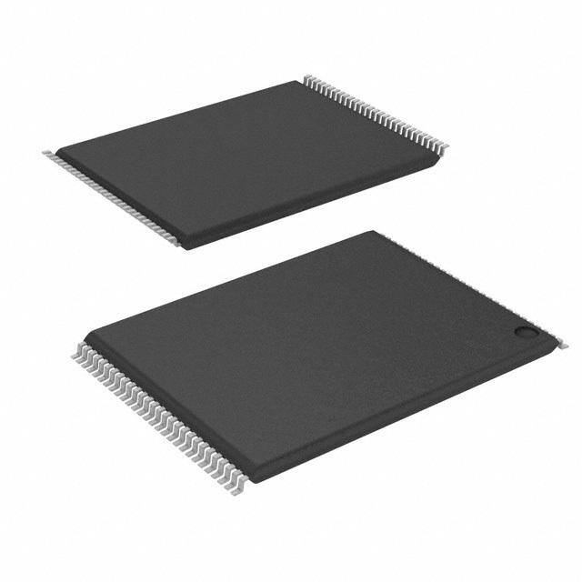
| 描述 | IC FLASH 256MBIT 110NS 56TSOP |
| 产品分类 | |
| 品牌 | Micron Technology Inc |
| 数据手册 | |
| 产品图片 |
|
| 产品型号 | JS28F256M29EWHA |
| rohs | 无铅 / 符合限制有害物质指令(RoHS)规范要求 |
| 产品系列 | - |
| 供应商器件封装 | 56-TSOP(14x20) |
| 其它名称 | 902049 |
| 包装 | 托盘 |
| 存储器类型 | FLASH - NOR |
| 存储容量 | 256M(32M x 8,16M x 16) |
| 封装/外壳 | 56-TFSOP(0.724",18.40mm 宽) |
| 工作温度 | -40°C ~ 85°C |
| 接口 | 并联 |
| 标准包装 | 576 |
| 格式-存储器 | 闪存 |
| 电压-电源 | 2.7 V ~ 3.6 V |
| 速度 | 110ns |


- 商务部:美国ITC正式对集成电路等产品启动337调查
- 曝三星4nm工艺存在良率问题 高通将骁龙8 Gen1或转产台积电
- 太阳诱电将投资9.5亿元在常州建新厂生产MLCC 预计2023年完工
- 英特尔发布欧洲新工厂建设计划 深化IDM 2.0 战略
- 台积电先进制程称霸业界 有大客户加持明年业绩稳了
- 达到5530亿美元!SIA预计今年全球半导体销售额将创下新高
- 英特尔拟将自动驾驶子公司Mobileye上市 估值或超500亿美元
- 三星加码芯片和SET,合并消费电子和移动部门,撤换高东真等 CEO
- 三星电子宣布重大人事变动 还合并消费电子和移动部门
- 海关总署:前11个月进口集成电路产品价值2.52万亿元 增长14.8%


PDF Datasheet 数据手册内容提取
256Mb, 512Mb, 1Gb, 2Gb: 3V Embedded Parallel NOR Flash Features Parallel NOR Flash Embedded Memory JS28F256M29EWxx, PC28F256M29EWxx, RC28F256M29EWxx JS28F512M29EWxx, PC28F512M29EWxx, RC28F512M29EWxx JS28F00AM29EWxx, PC28F00AM29EWxx, RC28F00AM29EWxx PC28F00BM29EWxx, RC28F00BM29EWxx Features • V /WP# pin protection PP – Protects first or last block regardless of block • 2Gb = stacked device (two 1Gb die) protection settings • Supply voltage • Software protection – VCC = 2.7–3.6V (program, erase, read) – Volatile protection – VCCQ = 1.65–VCC (I/O buffers) – Nonvolatile protection • Asynchronous random/page read – Password protection – Page size: 16 words or 32 bytes – Password access – Page access: 25ns • Extended memory block – Random access: 100ns (Fortified BGA); – 128-word (256-byte) block for permanent, secure 110ns (TSOP) identification • Buffer program: 512-word program buffer – Programmed or locked at the factory or by the • Program time customer – 0.88µs per byte (1.14 MB/s) TYP when using full • Low power consumption: Standby mode 512-word buffer size in buffer program • JESD47-compliant • Memory organization – 100,000 minimum ERASE cycles per block – Uniform blocks: 128-Kbytes or 64-Kwords each – Data retention: 20 years (TYP) • Program/erase controller • 65nm multilevel cell (MLC) process technology – Embedded byte (x8)/word (x16) program algo- • Package rithms – 56-pin TSOP, 14 x 20mm • Program/erase suspend and resume capability – 64-ball fortified BGA, 13 x 11mm – Read from another block during a PROGRAM • Green packages available SUSPEND operation – RoHS-compliant – Read or program another block during an ERASE – Halogen-free SUSPEND operation • Operating temperature • BLANK CHECK operation to verify an erased block – Ambient: –40°C to +85°C • Unlock bypass, block erase, chip erase, and write to buffer capability – Fast buffered/batch programming – Fast block/chip erase PDF: 09005aef849b4b09 1 Micron Technology, Inc. reserves the right to change products or specifications without notice. m29ew_256mb_2gb.pdf - Rev. E 11/16 EN © 2012 Micron Technology, Inc. All rights reserved. Products and specifications discussed herein are subject to change by Micron without notice.
256Mb, 512Mb, 1Gb, 2Gb: 3V Embedded Parallel NOR Flash Features Part Numbering Information Devices are shipped from the factory with memory content bits erased to 1. For available options, such as pack- ages or high/low protection, or for further information, contact your Micron sales representative. Part numbers can be verified at www.micron.com. Feature and specification comparison by device type is available at www.mi- cron.com/products. Contact the factory for devices not found. Table 1: Part Number Information Part Number Category Category Details Notes Package JS = 56-pin TSOP, 14mm x 20mm, lead-free, halogen-free, RoHS-compliant – PC = 64-ball Fortified BGA, 11mm x 13mm, lead-free, halogen-free, RoHS-compliant – RC = 64-ball Fortified BGA, 11mm x 13mm, leaded – Product designator 28F = NOR parallel interface – Density 256 = 256Mb – 512 = 512Mb – 00A = 1Gb – 00B = 2Gb – Device type M29EW = Embedded Flash memory (3V core, page, uniform block) – Device function H = Highest block protected by V /WP# 1 PP L = Lowest block protected by V /WP# – PP Features A/B/D/E or an asterisk (*) = Combination of features, including packing media, special – features, and specific customer request information Note: 1. For 2Gb device, H also indicates protection of the lowest block by VPP/WP#. Table 2: Standard Part Numbers by Density, Medium, and Package Package Density Medium JS PC RC 256Mb Tray JS28F256M29EWHA PC28F256M29EWHA RC28F256M29EWHA JS28F256M29EWLA PC28F256M29EWLA RC28F256M29EWLA Tape and Reel JS28F256M29EWHB PC28F256M29EWHB RC28F256M29EWHB JS28F256M29EWLB PC28F256M29EWLB – 512Mb Tray JS28F512M29EWHA PC28F512M29EWHD RC28F512M29EWHA JS28F512M29EWLA PC28F512M29EWLA RC28F512M29EWLA Tape and Reel JS28F512M29EWHB PC28F512M29EWHB RC28F512M29EWHB JS28F512M29EWLB PC28F512M29EWLB – 1Gb Tray JS28F00AM29EWHA PC28F00AM29EWHA RC28F00AM29EWHA JS28F00AM29EWLA PC28F00AM29EWLA RC28F00AM29EWLA Tape and Reel JS28F00AM29EWHB PC28F00AM29EWHB RC28F00AM29EWHB 2Gb Tray – PC28F00BM29EWHA RC28F00BM29EWHA PDF: 09005aef849b4b09 2 Micron Technology, Inc. reserves the right to change products or specifications without notice. m29ew_256mb_2gb.pdf - Rev. E 11/16 EN © 2012 Micron Technology, Inc. All rights reserved.
256Mb, 512Mb, 1Gb, 2Gb: 3V Embedded Parallel NOR Flash Features Table 3: Part Numbers with Security Features by Density, Medium, and Package Package Density Medium JS PC RC 256Mb Tray – PC28F256M29EWHD – – PC28F256M29EWLD – Tape and Reel – – – 512Mb Tray – PC28F512M29EWHA – – PC28F512M29EWLE – Tape and Reel – PC28F512M29EWHE – 1Gb Tray – PC28F00AM29EWHD – PC28F00AM29EWLE Tape and Reel – – – PDF: 09005aef849b4b09 3 Micron Technology, Inc. reserves the right to change products or specifications without notice. m29ew_256mb_2gb.pdf - Rev. E 11/16 EN © 2012 Micron Technology, Inc. All rights reserved.
256Mb, 512Mb, 1Gb, 2Gb: 3V Embedded Parallel NOR Flash Features Contents General Description ......................................................................................................................................... 8 Device Configurability .................................................................................................................................. 9 Signal Assignments ......................................................................................................................................... 10 Signal Descriptions ......................................................................................................................................... 12 Memory Organization .................................................................................................................................... 14 Memory Configuration ............................................................................................................................... 14 Memory Map ............................................................................................................................................. 14 Bus Operations ............................................................................................................................................... 15 Read .......................................................................................................................................................... 15 Write .......................................................................................................................................................... 15 Standby ..................................................................................................................................................... 16 Output Disable ........................................................................................................................................... 16 Reset .......................................................................................................................................................... 16 Registers ........................................................................................................................................................ 17 Data Polling Register .................................................................................................................................. 17 Lock Register .............................................................................................................................................. 21 Standard Command Definitions – Address-Data Cycles .................................................................................... 24 READ and AUTO SELECT Operations .............................................................................................................. 27 READ/RESET Command ............................................................................................................................ 27 READ CFI Command .................................................................................................................................. 27 AUTO SELECT Command ........................................................................................................................... 27 Bypass Operations .......................................................................................................................................... 29 UNLOCK BYPASS Command ...................................................................................................................... 29 UNLOCK BYPASS RESET Command ............................................................................................................ 29 Program Operations ....................................................................................................................................... 30 PROGRAM Command ................................................................................................................................ 30 UNLOCK BYPASS PROGRAM Command ..................................................................................................... 30 WRITE TO BUFFER PROGRAM Command .................................................................................................. 30 UNLOCK BYPASS WRITE TO BUFFER PROGRAM Command ....................................................................... 32 WRITE TO BUFFER PROGRAM CONFIRM Command .................................................................................. 33 BUFFERED PROGRAM ABORT AND RESET Command ................................................................................ 33 PROGRAM SUSPEND Command ................................................................................................................ 33 PROGRAM RESUME Command .................................................................................................................. 34 Erase Operations ............................................................................................................................................ 34 CHIP ERASE Command .............................................................................................................................. 34 UNLOCK BYPASS CHIP ERASE Command ................................................................................................... 34 BLOCK ERASE Command ........................................................................................................................... 35 UNLOCK BYPASS BLOCK ERASE Command ................................................................................................ 35 ERASE SUSPEND Command ....................................................................................................................... 36 ERASE RESUME Command ........................................................................................................................ 37 BLANK CHECK Operation .............................................................................................................................. 37 BLANK CHECK Commands ........................................................................................................................ 37 Block Protection Command Definitions – Address-Data Cycles ........................................................................ 38 Protection Operations .................................................................................................................................... 41 LOCK REGISTER Commands ...................................................................................................................... 41 PASSWORD PROTECTION Commands ....................................................................................................... 41 NONVOLATILE PROTECTION Commands .................................................................................................. 41 NONVOLATILE PROTECTION BIT LOCK BIT Commands ............................................................................ 44 VOLATILE PROTECTION Commands .......................................................................................................... 44 EXTENDED MEMORY BLOCK Commands .................................................................................................. 44 PDF: 09005aef849b4b09 4 Micron Technology, Inc. reserves the right to change products or specifications without notice. m29ew_256mb_2gb.pdf - Rev. E 11/16 EN © 2012 Micron Technology, Inc. All rights reserved.
256Mb, 512Mb, 1Gb, 2Gb: 3V Embedded Parallel NOR Flash Features EXIT PROTECTION Command .................................................................................................................... 45 Device Protection ........................................................................................................................................... 46 Hardware Protection .................................................................................................................................. 46 Software Protection .................................................................................................................................... 46 Volatile Protection Mode ............................................................................................................................. 47 Nonvolatile Protection Mode ...................................................................................................................... 47 Password Protection Mode .......................................................................................................................... 48 Password Access ......................................................................................................................................... 48 Common Flash Interface ................................................................................................................................ 50 Power-Up and Reset Characteristics ................................................................................................................ 54 Absolute Ratings and Operating Conditions ..................................................................................................... 56 DC Characteristics .......................................................................................................................................... 58 Read AC Characteristics .................................................................................................................................. 60 Write AC Characteristics ................................................................................................................................. 63 Accelerated Program, Data Polling/Toggle AC Characteristics ........................................................................... 71 Program/Erase Characteristics ........................................................................................................................ 73 Package Dimensions ....................................................................................................................................... 74 Additional Resources ...................................................................................................................................... 76 Revision History ............................................................................................................................................. 77 Rev. E – 11/16 ............................................................................................................................................. 77 Rev. D – 07/15 ............................................................................................................................................. 77 Rev. C – 09/14 ............................................................................................................................................. 77 Rev. B – 08/12 ............................................................................................................................................. 78 Rev. A – 04/12 ............................................................................................................................................. 78 PDF: 09005aef849b4b09 5 Micron Technology, Inc. reserves the right to change products or specifications without notice. m29ew_256mb_2gb.pdf - Rev. E 11/16 EN © 2012 Micron Technology, Inc. All rights reserved.
256Mb, 512Mb, 1Gb, 2Gb: 3V Embedded Parallel NOR Flash Features List of Figures Figure 1: Logic Diagram ................................................................................................................................... 8 Figure 2: Dual Die Configuration – 2Gb ............................................................................................................ 9 Figure 3: Single Die Configuration – Lower Densities ........................................................................................ 9 Figure 4: 56-Pin TSOP (Top View) .................................................................................................................. 10 Figure 5: 64-Ball Fortified BGA ....................................................................................................................... 11 Figure 6: Data Polling Flowchart .................................................................................................................... 19 Figure 7: Toggle Bit Flowchart ........................................................................................................................ 20 Figure 8: Data Polling/Toggle Bit Flowchart .................................................................................................... 21 Figure 9: Lock Register Program Flowchart ..................................................................................................... 23 Figure 10: Boundary Condition of Program Buffer Size .................................................................................... 31 Figure 11: WRITE TO BUFFER PROGRAM Flowchart ...................................................................................... 32 Figure 12: Set/Clear Nonvolatile Protection Bit Algorithm Flowchart ............................................................... 43 Figure 13: Software Protection Scheme .......................................................................................................... 48 Figure 14: Power-Up Timing .......................................................................................................................... 54 Figure 15: Reset AC Timing – No PROGRAM/ERASE Operation in Progress ...................................................... 55 Figure 16: Reset AC Timing During PROGRAM/ERASE Operation .................................................................... 55 Figure 17: AC Measurement Load Circuit ....................................................................................................... 57 Figure 18: AC Measurement I/O Waveform ..................................................................................................... 57 Figure 19: Random Read AC Timing (8-Bit Mode) ........................................................................................... 61 Figure 20: Random Read AC Timing (16-Bit Mode) ......................................................................................... 61 Figure 21: BYTE# Transition Read AC Timing .................................................................................................. 62 Figure 22: Page Read AC Timing ..................................................................................................................... 62 Figure 23: WE#-Controlled Program AC Timing (8-Bit Mode) .......................................................................... 64 Figure 24: WE#-Controlled Program AC Timing (16-Bit Mode) ......................................................................... 65 Figure 25: CE#-Controlled Program AC Timing (8-Bit Mode) ........................................................................... 67 Figure 26: CE#-Controlled Program AC Timing (16-Bit Mode) ......................................................................... 68 Figure 27: Chip/Block Erase AC Timing (8-Bit Mode) ...................................................................................... 69 Figure 28: Chip/Block Erase AC Timing (16-Bit Mode) .................................................................................... 70 Figure 29: Accelerated Program AC Timing ..................................................................................................... 71 Figure 30: Data Polling AC Timing .................................................................................................................. 71 Figure 31: Toggle/Alternative Toggle Bit Polling AC Timing .............................................................................. 72 Figure 32: 56-Pin TSOP – 14mm x 20mm ........................................................................................................ 74 Figure 33: 64-Ball Fortified BGA – 11mm x 13mm ........................................................................................... 75 PDF: 09005aef849b4b09 6 Micron Technology, Inc. reserves the right to change products or specifications without notice. m29ew_256mb_2gb.pdf - Rev. E 11/16 EN © 2012 Micron Technology, Inc. All rights reserved.
256Mb, 512Mb, 1Gb, 2Gb: 3V Embedded Parallel NOR Flash Features List of Tables Table 1: Part Number Information ................................................................................................................... 2 Table 2: Standard Part Numbers by Density, Medium, and Package ................................................................... 2 Table 3: Part Numbers with Security Features by Density, Medium, and Package ................................................ 3 Table 4: Signal Descriptions ........................................................................................................................... 12 Table 5: Blocks[2047:0] .................................................................................................................................. 14 Table 6: Bus Operations ................................................................................................................................. 15 Table 7: Data Polling Register Bit Definitions .................................................................................................. 17 Table 8: Operations and Corresponding Bit Settings ........................................................................................ 18 Table 9: Lock Register Bit Definitions ............................................................................................................. 22 Table 10: Standard Command Definitions – Address-Data Cycles, 8-Bit and 16-Bit ........................................... 24 Table 11: Read Electronic Signature ............................................................................................................... 28 Table 12: Block Protection ............................................................................................................................. 28 Table 13: Block Protection Command Definitions – Address-Data Cycles, 8-Bit and 16-Bit ................................ 38 Table 14: Extended Memory Block Address and Data ...................................................................................... 44 Table 15: V /WP# Functions ......................................................................................................................... 46 PP Table 16: Block Protection Status ................................................................................................................... 49 Table 17: Query Structure Overview ............................................................................................................... 50 Table 18: CFI Query Identification String ........................................................................................................ 50 Table 19: CFI Query System Interface Information .......................................................................................... 51 Table 20: Device Geometry Definition ............................................................................................................ 51 Table 21: Primary Algorithm-Specific Extended Query Table ........................................................................... 52 Table 22: Power-Up Specifications ................................................................................................................. 54 Table 23: Reset AC Specifications ................................................................................................................... 55 Table 24: Absolute Maximum/Minimum Ratings ............................................................................................ 56 Table 25: Operating Conditions ...................................................................................................................... 56 Table 26: Input/Output Capacitance .............................................................................................................. 57 Table 27: DC Current Characteristics .............................................................................................................. 58 Table 28: DC Voltage Characteristics .............................................................................................................. 59 Table 29: Read AC Characteristics .................................................................................................................. 60 Table 30: WE#-Controlled Write AC Characteristics ......................................................................................... 63 Table 31: CE#-Controlled Write AC Characteristics ......................................................................................... 66 Table 32: Accelerated Program and Data Polling/Data Toggle AC Characteristics .............................................. 71 Table 33: Program/Erase Characteristics ........................................................................................................ 73 Table 34: Technical Notes .............................................................................................................................. 76 PDF: 09005aef849b4b09 7 Micron Technology, Inc. reserves the right to change products or specifications without notice. m29ew_256mb_2gb.pdf - Rev. E 11/16 EN © 2012 Micron Technology, Inc. All rights reserved.
256Mb, 512Mb, 1Gb, 2Gb: 3V Embedded Parallel NOR Flash General Description General Description The device is an asynchronous, uniform block, parallel NOR Flash memory device. READ, ERASE, and PROGRAM operations are performed using a single low-voltage sup- ply. Upon power-up, the device defaults to read array mode. The main memory array is divided into uniform blocks that can be erased independent- ly so that valid data can be preserved while old data is purged. PROGRAM and ERASE commands are written to the command interface of the memory. An on-chip program/ erase controller simplifies the process of programming or erasing the memory by taking care of all special operations required to update the memory contents. The end of a PROGRAM or ERASE operation can be detected and any error condition can be identi- fied. The command set required to control the device is consistent with JEDEC stand- ards. CE#, OE#, and WE# control the bus operation of the device and enable a simple con- nection to most microprocessors, often without additional logic. The device supports asynchronous random read and page read from all blocks of the array. It also features an internal program buffer that improves throughput by program- ming 512 words via one command sequence. A 128-word extended memory block over- laps addresses with array block 0. Users can program this additional space and then protect it to permanently secure the contents. The device also features different levels of hardware and software protection to secure blocks from unwanted modification. Note: For a 2Gb device, A[26] = V selects the upper die and A[26] = V selects the lower IH IL die. Setup commands should be re-issued to the device when a different die is selected. Figure 1: Logic Diagram V V V /WP# CC CCQ PP 15 A[MAX:0] DQ[14:0] WE# DQ15/A-1 CE# OE# RY/BY# RST# BYTE# V SS PDF: 09005aef849b4b09 8 Micron Technology, Inc. reserves the right to change products or specifications without notice. m29ew_256mb_2gb.pdf - Rev. E 11/16 EN © 2012 Micron Technology, Inc. All rights reserved.
256Mb, 512Mb, 1Gb, 2Gb: 3V Embedded Parallel NOR Flash General Description Device Configurability Figure 2: Dual Die Configuration – 2Gb CE# V /WP# PP Upper die OE# V (1Gb) CC WE# V CCQ RST# VSS DQ[14:0] BYTE# Lower die DQ15/A-1 (1Gb) A[26:0] RY/BY# Note: 1. A[26] = VIH selects the upper die; A[26] = VIL selects the lower die. Figure 3: Single Die Configuration – Lower Densities V V V /WP# CC CCQ PP 15 A[MAX:0] DQ[14:0] WE# DQ15/A-1 CE# OE# RY/BY# RST# BYTE# V SS PDF: 09005aef849b4b09 9 Micron Technology, Inc. reserves the right to change products or specifications without notice. m29ew_256mb_2gb.pdf - Rev. E 11/16 EN © 2012 Micron Technology, Inc. All rights reserved.
256Mb, 512Mb, 1Gb, 2Gb: 3V Embedded Parallel NOR Flash Signal Assignments Signal Assignments Figure 4: 56-Pin TSOP (Top View) A23 1 56 A24 A22 2 55 A25 A15 3 54 A16 A14 4 53 BYTE# A13 5 52 VSS A12 6 51 DQ15/A-1 A11 7 50 DQ7 A10 8 49 DQ14 A9 9 48 DQ6 A8 10 47 DQ13 A19 11 46 DQ5 A20 12 45 DQ12 WE# 13 44 DQ4 RST# 14 43 V CC A21 15 42 DQ11 V /WP# 16 41 DQ3 PP RY/BY# 17 40 DQ10 A18 18 39 DQ2 A17 19 38 DQ9 A7 20 37 DQ1 A6 21 36 DQ8 A5 22 35 DQ0 A4 23 34 OE# A3 24 33 V SS A2 25 32 CE# A1 26 31 A0 RFU 27 30 RFU RFU 28 29 V CCQ Notes: 1. A-1 is the least significant address bit in x8 mode. 2. A23 is valid for 256Mb and above; otherwise, it is RFU. 3. A24 is valid for 512Mb and above; otherwise, it is RFU. 4. A25 is valid for 1Gb and above; otherwise, it is RFU. PDF: 09005aef849b4b09 10 Micron Technology, Inc. reserves the right to change products or specifications without notice. m29ew_256mb_2gb.pdf - Rev. E 11/16 EN © 2012 Micron Technology, Inc. All rights reserved.
256Mb, 512Mb, 1Gb, 2Gb: 3V Embedded Parallel NOR Flash Signal Assignments Figure 5: 64-Ball Fortified BGA 1 2 3 4 5 6 7 8 A RFU A3 A7 RY/BY#WE# A9 A13 RFU B A26 A4 A17V /WP#RST# A8 A12 A22 PP C RFU A2 A6 A18 A21 A10 A14 A23 D RFU A1 A5 A20 A19 A11 A15 V CCQ E RFU A0 D0 D2 D5 D7 A16 V SS F V CE# D8 D10 D12 D14 BYTE# A24 CCQ G RFU OE# D9 D11 V D13 D15/A-1 A25 CC H RFU V D1 D3 D4 D6 V RFU SS SS Top view – ball side down Notes: 1. A-1 is the least significant address bit in x8 mode. 2. A23 is valid for 256Mb and above; otherwise, it is RFU. 3. A24 is valid for 512Mb and above; otherwise, it is RFU. 4. A25 is valid for 1Gb and above; otherwise, it is RFU. 5. A26 is valid for 2Gb only; otherwise it is RFU. PDF: 09005aef849b4b09 11 Micron Technology, Inc. reserves the right to change products or specifications without notice. m29ew_256mb_2gb.pdf - Rev. E 11/16 EN © 2012 Micron Technology, Inc. All rights reserved.
256Mb, 512Mb, 1Gb, 2Gb: 3V Embedded Parallel NOR Flash Signal Descriptions Signal Descriptions The signal description table below is a comprehensive list of signals for this device fami- ly. All signals listed may not be supported on this device. See Signal Assignments for in- formation specific to this device. Table 4: Signal Descriptions Name Type Description A[MAX:0] Input Address: Selects the cells in the array to access during READ operations. During WRITE oper- ations, they control the commands sent to the command interface of the program/erase con- troller. CE# Input Chip enable: Activates the device, enabling READ and WRITE operations to be performed. When CE# is HIGH, the device goes to standby and data outputs are High-Z. OE# Input Output enable: Active LOW input. OE# LOW enables the data output buffers during READ cycles. When OE# is HIGH, data outputs are High-Z. WE# Input Write enable: Controls WRITE operations to the device. Address is latched on the falling edge of WE# and data is latched on the rising edge. V /WP# Input V /Write Protect: Provides WRITE PROTECT function and V function. These functions PP PP PPH protect the lowest or highest block and enable the device to enter unlock bypass mode, re- spectively. (Refer to Hardware Protection and Bypass Operations for details.) BYTE# Input Byte/word organization select: Switches between x8 and x16 bus modes. When BYTE# is LOW, the device is in x8 mode; when HIGH, the device is in x16 mode. Under byte configura- tion, BYTE# should not be toggled during any WRITE operation. Caution: This pin cannot be floated. RST# Input Reset: Applies a hardware reset to the device control logic and places it in standby, which is achieved by holding RST# LOW for at least tPLPH. After RST# goes HIGH, the device is ready for READ and WRITE operations (after tPHEL or tPHWL, whichever occurs last). DQ[7:0] I/O Data I/O: Outputs the data stored at the selected address during a READ operation. During WRITE operations, they represent the commands sent to the command interface of the inter- nal state machine. DQ[14:8] I/O Data I/O: Outputs the data stored at the selected address during a READ operation when BYTE# is HIGH. When BYTE# is LOW, these pins are not used and are High-Z. During WRITE operations, these bits are not used. When reading the data polling register, these bits should be ignored. DQ15/A-1 I/O Data I/O or address input: When the device operates in x16 bus mode, this pin behaves as data I/O, together with DQ[14:8]. When the device operates in x8 bus mode, this pin behaves as the least significant bit of the address. Except where stated explicitly otherwise, DQ15 = data I/O (x16 mode); A-1 = address input (x8 mode). RY/BY# Output Ready busy: Open-drain output that can be used to identify when the device is performing a PROGRAM or ERASE operation. During PROGRAM or ERASE operations, RY/BY# is LOW, and is High-Z during read mode, auto select mode, and erase suspend mode. The use of an open-drain output enables the RY/BY# pins from several devices to be connec- ted to a single pull-up resistor to V . A low value will then indicate that one (or more) of CCQ the devices is (are) busy. A 10K Ohm or bigger resistor is recommended as pull-up resistor to achieve 0.1V V . OL PDF: 09005aef849b4b09 12 Micron Technology, Inc. reserves the right to change products or specifications without notice. m29ew_256mb_2gb.pdf - Rev. E 11/16 EN © 2012 Micron Technology, Inc. All rights reserved.
256Mb, 512Mb, 1Gb, 2Gb: 3V Embedded Parallel NOR Flash Signal Descriptions Table 4: Signal Descriptions (Continued) Name Type Description V Supply Supply voltage: Provides the power supply for READ, PROGRAM, and ERASE operations. CC The device is disabled when V ≤ V . If the program/erase controller is programming or CC LKO erasing during this time, then the operation aborts and the contents being altered will be invalid. A 0.1μF and 0.01µF capacitor should be connected between V and V to decouple the cur- CC SS rent surges from the power supply. The PCB track widths must be sufficient to carry the cur- rents required during PROGRAM and ERASE operations (see DC Characteristics). V Supply I/O supply voltage: Provides the power supply to the I/O pins and enables all outputs to be CCQ powered independently from V . CC A 0.1μF and 0.01µF capacitor should be connected between V and V to decouple the CCQ SS current surges from the power supply. V Supply Ground: All V pins must be connected to the system ground. SS SS RFU — Reserved for future use: Reserved by Micron for future device functionality and enhance- ment. These should be treated in the same way as a DNU signal. DNU — Do not use: Do not connect to any other signal, or power supply; must be left floating. NC — No connect: No internal connection; can be driven or floated. PDF: 09005aef849b4b09 13 Micron Technology, Inc. reserves the right to change products or specifications without notice. m29ew_256mb_2gb.pdf - Rev. E 11/16 EN © 2012 Micron Technology, Inc. All rights reserved.
256Mb, 512Mb, 1Gb, 2Gb: 3V Embedded Parallel NOR Flash Memory Organization Memory Organization Memory Configuration The main memory array is divided into 128KB or 64KW uniform blocks. Memory Map Table 5: Blocks[2047:0] Block Address Range (x8) Block Address Range (x16) Block Size Start End Size Start End 2047 128KB FFE 0000h FFF FFFFh 64KW 7FF 0000h 7FF FFFFh ⋮ ⋮ ⋮ ⋮ ⋮ 1023 7FE 0000h 7FF FFFFh 3FF 0000h 3FF FFFFh ⋮ ⋮ ⋮ ⋮ ⋮ 511 3FE 0000h 3FF FFFFh 1FF 0000h 1FF FFFFh ⋮ ⋮ ⋮ ⋮ ⋮ 255 1FE 0000h 1FF FFFFh 0FF 0000h 0FF FFFFh ⋮ ⋮ ⋮ ⋮ ⋮ 127 0FE 0000h 0FF FFFFh 07F 0000h 07F FFFFh ⋮ ⋮ ⋮ ⋮ ⋮ 63 07E 0000h 07F FFFFh 03F 0000h 03F FFFFh ⋮ ⋮ ⋮ ⋮ ⋮ 0 000 0000h 001 FFFFh 000 0000h 000 FFFFh Note: 1. 128Mb device = Blocks 0–127; 256Mb device = Blocks 0–255; 512Mb device = Blocks 0– 511; 1Gb device = Blocks 0–1023; 2Gb device = Blocks 0–2047. PDF: 09005aef849b4b09 14 Micron Technology, Inc. reserves the right to change products or specifications without notice. m29ew_256mb_2gb.pdf - Rev. E 11/16 EN © 2012 Micron Technology, Inc. All rights reserved.
256Mb, 512Mb, 1Gb, 2Gb: 3V Embedded Parallel NOR Flash Bus Operations Bus Operations Table 6: Bus Operations Notes 1 and 2 apply to entire table 8-Bit Mode 16-Bit Mode A[MAX:0], DQ15/A-1, Operation CE# OE# WE# RST# V /WP# DQ15/A-1 DQ[14:8] DQ[7:0] A[MAX:0] DQ[14:0] PP READ L L H H X Cell address High-Z Data output Cell address Data output WRITE L H L H H3 Command High-Z Data input4 Command Data input4 address address STANDBY H X X H X X High-Z High-Z X High-Z OUTPUT L H H H X X High-Z High-Z X High-Z DISABLE RESET X X X L X X High-Z High-Z X High-Z Notes: 1. Typical glitches of less than 3ns on CE#, OE#, WE#, and RST# are ignored by the device and do not affect bus operations. 2. H = Logic level HIGH (V ); L = Logic level LOW (V ); X = HIGH or LOW. IH IL 3. If WP# is LOW, then the highest or the lowest block remains protected, depending on line item. 4. Data input is required when issuing a command sequence or when performing data polling or block protection. Read Bus READ operations read from the memory cells, registers, or CFI space. To accelerate the READ operation, the memory array can be read in page mode where data is inter- nally read and stored in a page buffer. Page size is 16 words (32 bytes) and is addressed by address inputs A[3:0] in x16 bus mode and A[3:0] plus DQ15/A-1 in x8 bus mode. The extended memory blocks and CFI area do not support page read mode. A valid bus READ operation involves setting the desired address on the address inputs, taking CE# and OE# LOW, and holding WE# HIGH. The data I/Os will output the value. If CE# goes HIGH and returns LOW for a subsequent access, a random read access is perform and tACC or tCE is required. (See AC Characteristics for details about when the output becomes valid.) Write Bus WRITE operations write to the command interface. A valid bus WRITE operation begins by setting the desired address on the address inputs. The address inputs are latched by the command interface on the falling edge of CE# or WE#, whichever occurs last. The data I/Os are latched by the command interface on the rising edge of CE# or WE#, whichever occurs first. OE# must remain HIGH during the entire bus WRITE oper- ation (See AC Characteristics for timing requirement details). PDF: 09005aef849b4b09 15 Micron Technology, Inc. reserves the right to change products or specifications without notice. m29ew_256mb_2gb.pdf - Rev. E 11/16 EN © 2012 Micron Technology, Inc. All rights reserved.
256Mb, 512Mb, 1Gb, 2Gb: 3V Embedded Parallel NOR Flash Bus Operations Standby Driving CE# HIGH in read mode causes the device to enter standby and data I/Os to be High-Z (See DC Characteristics). During PROGRAM or ERASE operations, the device will continue to use the program/ erase supply current (I ) until the operation completes. When CE# is HIGH, the de- CC3 vice cannot be placed into standby mode during a PROGRAM/ERASE operation. Output Disable Data I/Os are High-Z when OE# is HIGH. Reset During reset mode the device is deselected and the outputs are High-Z. The device is in reset mode when RST# is LOW. The power consumption is reduced to the standby level, independently from CE#, OE#, or WE# inputs. When RST# is HIGH, a time of tPHEL is required before a READ operation can access the device, and a delay of tPHWL is required before a write sequence can be initiated. After this wake-up interval, normal operation is restored, the device defaults to read ar- ray mode, and the data polling register is reset. If RST# is driven LOW during a PROGRAM/ERASE operation or any other operation that requires writing to the device, the operation will abort within tPLRH, and memory con- tents at the aborted block or address are no longer valid. PDF: 09005aef849b4b09 16 Micron Technology, Inc. reserves the right to change products or specifications without notice. m29ew_256mb_2gb.pdf - Rev. E 11/16 EN © 2012 Micron Technology, Inc. All rights reserved.
256Mb, 512Mb, 1Gb, 2Gb: 3V Embedded Parallel NOR Flash Registers Registers Data Polling Register Table 7: Data Polling Register Bit Definitions Note 1 applies to entire table Bit Name Settings Description Notes DQ7 Data polling 0 or 1, depending on Monitors whether the program/erase controller has successful- 2, 4 bit operations ly completed its operation, or has responded to an ERASE SUS- PEND operation. DQ6 Toggle bit Toggles: 0 to 1; 1 to 0; Monitors whether the program, erase, or blank check control- 3, 4, 5 and so on ler has successfully completed its operations, or has responded to an ERASE SUSPEND operation. During a PROGRAM/ERASE/ BLANK CHECK operation, DQ6 toggles from 0 to 1, 1 to 0, and so on, with each successive READ operation from any address. DQ5 Error bit 0 = Success Identifies errors detected by the program/erase controller. DQ5 4, 6 1 = Failure is set to 1 when a PROGRAM, BLOCK ERASE, or CHIP ERASE op- eration fails to write the correct data to the memory, or when a BLANK CHECK operation fails. DQ3 Erase timer 0 = Erase not in progress Identifies the start of program/erase controller operation dur- 4 bit 1 = Erase in progress ing a BLOCK ERASE command. Before the program/erase con- troller starts, this bit set to 0, and additional blocks to be erased can be written to the command interface. DQ2 Alternative Toggles: 0 to 1; 1 to 0; During CHIP ERASE, BLOCK ERASE, and ERASE SUSPEND opera- 3, 4 toggle bit and so on tions, DQ2 toggles from 0 to 1, 1 to 0, and so on, with each successive READ operation from addresses within the blocks being erased. DQ1 Buffered 1 = Abort Indicates a BUFFER PROGRAM operation abort. The BUFFERED program PROGRAM ABORT and RESET command must be issued to re- abort bit turn the device to read mode (see WRITE TO BUFFER PRO- GRAM command). Notes: 1. The data polling register can be read during PROGRAM, ERASE, or ERASE SUSPEND op- erations; the READ operation outputs data on DQ[7:0]. 2. For a PROGRAM operation in progress, DQ7 outputs the complement of the bit being programmed. For a BUFFER PROGRAM operation, DQ7 outputs the complement of the bit for the last word being programmed in the write buffer. For a READ operation from the address previously programmed successfully, DQ7 outputs existing DQ7 data. For a READ operation from addresses with blocks to be erased while an ERASE SUSPEND oper- ation is in progress, DQ7 outputs 0; upon successful completion of the ERASE SUSPEND operation, DQ7 outputs 1. For an ERASE operation in progress, DQ7 outputs 0; upon ERASE operation's successful completion, DQ7 outputs 1. 3. After successful completion of a PROGRAM, ERASE, or BLANK CHECK operation, the de- vice returns to read mode. 4. During erase suspend mode, READ operations to addresses within blocks not being erased output memory array data as if in read mode. A protected block is treated the same as a block not being erased. See the Toggle Flowchart for more information. PDF: 09005aef849b4b09 17 Micron Technology, Inc. reserves the right to change products or specifications without notice. m29ew_256mb_2gb.pdf - Rev. E 11/16 EN © 2012 Micron Technology, Inc. All rights reserved.
256Mb, 512Mb, 1Gb, 2Gb: 3V Embedded Parallel NOR Flash Registers 5. During erase suspend mode, DQ6 toggles when addressing a cell within a block being erased. The toggling stops when the program/erase controller has suspended the ERASE operation. See the Toggle Flowchart for more information. 6. When DQ5 is set to 1, a READ/RESET (F0h) command must be issued before any subse- quent command. Table 8: Operations and Corresponding Bit Settings Note 1 applies to entire table Operation Address DQ7 DQ6 DQ5 DQ3 DQ2 DQ1 RY/BY# Notes PROGRAM Any address DQ7# Toggle 0 – – 0 0 2 BLANK CHECK Any address 1 Toggle 0 – – 0 0 CHIP ERASE Any address 0 Toggle 0 1 Toggle – 0 BLOCK ERASE Erasing block 0 Toggle 0 0 Toggle – 0 before time-out Non-erasing block 0 Toggle 0 0 No toggle – 0 BLOCK ERASE Erasing block 0 Toggle 0 1 Toggle – 0 Non-erasing block 0 Toggle 0 1 No toggle – 0 PROGRAM Programming Invalid operation High-Z SUSPEND block Nonprogramming Outputs memory array data as if in read mode High-Z block ERASE Erasing block 1 No Toggle 0 – Toggle – High-Z SUSPEND Non-erasing block Outputs memory array data as if in read mode High-Z PROGRAM during Erasing block DQ7# Toggle 0 – Toggle – 0 2 ERASE SUSPEND Non-erasing block DQ7# Toggle 0 – No Toggle – 0 2 BUFFERED Any address DQ7# Toggle 0 – – 1 High-Z PROGRAM ABORT PROGRAM Error Any address DQ7# Toggle 1 – – – High-Z 2 ERASE Error Any address 0 Toggle 1 1 Toggle – High-Z BLANK CHECK Er- Any address 0 Toggle 1 1 Toggle – High-Z ror Notes: 1. Unspecified data bits should be ignored. 2. DQ7# for buffer program is related to the last address location loaded. PDF: 09005aef849b4b09 18 Micron Technology, Inc. reserves the right to change products or specifications without notice. m29ew_256mb_2gb.pdf - Rev. E 11/16 EN © 2012 Micron Technology, Inc. All rights reserved.
256Mb, 512Mb, 1Gb, 2Gb: 3V Embedded Parallel NOR Flash Registers Figure 6: Data Polling Flowchart Start Read DQ7, DQ5, and DQ1 at valid address1 Yes DQ7 = Data No No No DQ1 = 13 DQ5 = 12 Yes Yes Read DQ7 at valid address Yes DQ7 = Data No Failure 4 Success Notes: 1. Valid address is the address being programmed or an address within the block being erased. 2. Failure results: DQ5 = 1 indicates an operation error. A READ/RESET command must be issued before any subsequent command. 3. DQ1 = 1 indicates a WRITE TO BUFFER PROGRAM ABORT operation. A full three-cycle RESET (AAh/55h/F0h) command sequence must be used to reset the aborted device. 4. The data polling process does not support the BLANK CHECK operation. The process represented in the Toggle Bit Flowchart figure can provide information on the BLANK CHECK operation. PDF: 09005aef849b4b09 19 Micron Technology, Inc. reserves the right to change products or specifications without notice. m29ew_256mb_2gb.pdf - Rev. E 11/16 EN © 2012 Micron Technology, Inc. All rights reserved.
256Mb, 512Mb, 1Gb, 2Gb: 3V Embedded Parallel NOR Flash Registers Figure 7: Toggle Bit Flowchart Start Read DQ6 at valid address Read DQ6, DQ5, and DQ1 at valid address No DQ6 = Toggle Yes No No DQ1 = 1 DQ5 = 1 Yes Yes Read DQ6 (twice) at valid address No DQ6 = Toggle Yes Failure1 Success Notes: 1. Failure results: DQ5 = 1 indicates an operation error; DQ1 = 1 indicates a WRITE TO BUF- FER PROGRAM ABORT operation. 2. The toggle bit process supports the BLANK CHECK operation. PDF: 09005aef849b4b09 20 Micron Technology, Inc. reserves the right to change products or specifications without notice. m29ew_256mb_2gb.pdf - Rev. E 11/16 EN © 2012 Micron Technology, Inc. All rights reserved.
256Mb, 512Mb, 1Gb, 2Gb: 3V Embedded Parallel NOR Flash Registers Figure 8: Data Polling/Toggle Bit Flowchart Start Read 1 Yes Yes Yes DQ7 = Valid data Read 2 Read 3 PROGRAM operation Read 3 correct data? No No No PROGRAM operation Yes DQ5 = 1 Read 2 failure No DQ6 = Toggling Yes Device error Read 3 Read2.DQ6 = Read3.DQ6 No DQ6 = Toggling Yes Timeout failure DQ2 = Toggling Yes Erase/suspend mode Read1.DQ6 = Read2.DQ6 Read2.DQ2 = Read3.DQ2 No No ERASE operation PROGRAM operation Device busy: Repolling complete complete Yes Yes WRITE TO BUFFER WRITE TO BUFFER DQ1 = 1 PROGRAM PROGRAM abort No No Device busy: Repolling Lock Register PDF: 09005aef849b4b09 21 Micron Technology, Inc. reserves the right to change products or specifications without notice. m29ew_256mb_2gb.pdf - Rev. E 11/16 EN © 2012 Micron Technology, Inc. All rights reserved.
256Mb, 512Mb, 1Gb, 2Gb: 3V Embedded Parallel NOR Flash Registers Table 9: Lock Register Bit Definitions Note 1 applies to entire table Bit Name Settings Description Notes DQ2 Password 0 = Password protection Places the device permanently in password protection mode. 2 protection mode enabled mode lock bit 1 = Password protection mode disabled (Default) DQ1 Nonvolatile 0 = Nonvolatile protection Places the device in nonvolatile protection mode with pass- 2 protection mode enabled with pass- word protection mode permanently disabled. When shipped mode lock bit word protection mode from the factory, the device will operate in nonvolatile protec- permanently disabled tion mode, and the memory blocks are unprotected. 1 = Nonvolatile protection mode enabled (Default) DQ0 Extended 0 = Protected If the device is shipped with the extended memory block un- memory 1 = Unprotected (Default) locked, the block can be protected by setting this bit to 0. The block extended memory block protection status can be read in auto protection bit select mode by issuing an AUTO SELECT command. Notes: 1. The lock register is a 16-bit, one-time programmable register. DQ[15:3] are reserved and are set to a default value of 1. 2. The password protection mode lock bit and nonvolatile protection mode lock bit cannot both be programmed to 0. Any attempt to program one while the other is programmed causes the operation to abort, and the device returns to read mode. The device is ship- ped from the factory with the default setting. PDF: 09005aef849b4b09 22 Micron Technology, Inc. reserves the right to change products or specifications without notice. m29ew_256mb_2gb.pdf - Rev. E 11/16 EN © 2012 Micron Technology, Inc. All rights reserved.
256Mb, 512Mb, 1Gb, 2Gb: 3V Embedded Parallel NOR Flash Registers Figure 9: Lock Register Program Flowchart Start Enter LOCK REGISTER command set Address/data (unlock) cycle 1 Address/data (unlock) cycle 2 Address/data cycle 3 PROGRAM LOCK REGISTER Address/data cycle 1 Address/data cycle 2 Polling algorithm No Done? Yes Read lock register No Match expected value, 0? Yes Success: EXIT PROTECTION command set Address/data cycle 1 Address/data cycle 2 Notes: 1. Each lock register bit can be programmed only once. 2. See the Block Protection Command Definitions table for address-data cycle details. 3. DQ5 and DQ1 are ignored in this algorithm flow. PDF: 09005aef849b4b09 23 Micron Technology, Inc. reserves the right to change products or specifications without notice. m29ew_256mb_2gb.pdf - Rev. E 11/16 EN © 2012 Micron Technology, Inc. All rights reserved.
256Mb, 512Mb, 1Gb, 2Gb: 3V Embedded Parallel NOR Flash Standard Command Definitions – Address-Data Cycles Standard Command Definitions – Address-Data Cycles Table 10: Standard Command Definitions – Address-Data Cycles, 8-Bit and 16-Bit Note 1 applies to entire table Address and Data Cycles Command and Bus 1st 2nd 3rd 4th 5th 6th Code/Subcode Size A D A D A D A D A D A D Notes READ and AUTO SELECT Operations READ/RESET (F0h) x8 X F0 2 AAA AA 555 55 X F0 x16 X F0 555 AA 2AA 55 X F0 READ CFI (98h) x8 AAA 98 x16 555 AUTO SELECT (90h) x8 AAA AA 555 55 AAA 90 Note Note 4, 5 x16 555 2AA 555 3 3 BYPASS Operations UNLOCK BYPASS (20h) x8 AAA AA 555 55 AAA 20 x16 555 2AA 555 UNLOCK BYPASS x8 X 90 X 00 RESET (90h/00h) x16 PROGRAM Operations PROGRAM (A0h) x8 AAA AA 555 55 AAA A0 PA PD x16 555 2AA 555 UNLOCK BYPASS x8 X A0 PA PD 6 PROGRAM (A0h) x16 WRITE TO BUFFER x8 AAA AA 555 55 BAd 25 BAd N PA PD 7, 8, 9 PROGRAM (25h) x16 555 2AA UNLOCK BYPASS x8 BAd 25 BAd N PA PD 6 WRITE TO BUFFER x16 PROGRAM (25h) WRITE TO BUFFER x8 BAd 29 7 PROGRAM CONFIRM x16 (29h) BUFFERED PROGRAM x8 AAA AA 555 55 AAA F0 ABORT and RESET (F0h) x16 555 2AA 555 PROGRAM SUSPEND x8 X B0 (B0h) x16 PROGRAM RESUME x8 X 30 (30h) x16 ERASE Operations PDF: 09005aef849b4b09 24 Micron Technology, Inc. reserves the right to change products or specifications without notice. m29ew_256mb_2gb.pdf - Rev. E 11/16 EN © 2012 Micron Technology, Inc. All rights reserved.
256Mb, 512Mb, 1Gb, 2Gb: 3V Embedded Parallel NOR Flash Standard Command Definitions – Address-Data Cycles Table 10: Standard Command Definitions – Address-Data Cycles, 8-Bit and 16-Bit (Continued) Note 1 applies to entire table Address and Data Cycles Command and Bus 1st 2nd 3rd 4th 5th 6th Code/Subcode Size A D A D A D A D A D A D Notes CHIP ERASE (80/10h) x8 AAA AA 555 55 AAA 80 AAA AA 555 55 AAA 10 x16 555 2AA 555 555 2AA 555 UNLOCK BYPASS x8 X 80 X 10 6 CHIP ERASE (80/10h) x16 BLOCK ERASE (80/30h) x8 AAA AA 555 55 AAA 80 AAA AA 555 55 BAd 30 10 x16 555 2AA 555 555 2AA UNLOCK BYPASS x8 X 80 BAd 30 6 BLOCK ERASE (80/30h) x16 ERASE SUSPEND (B0h) x8 X B0 x16 ERASE RESUME (30h) x8 X 30 x16 BLANK CHECK Operations BLANK CHECK x8 AAA AA 555 55 BAd EB BAd 76 BAd 00 BAd 00 SETUP (EB/76h) x16 555 2AA BLANK CHECK CONFIRM x8 BAd 29 and READ (29h) x16 Notes: 1. A = Address; D = Data; X = "Don't Care;" BAd = Any address in the block; N + 1 = num- ber of words (x16)/bytes (x8) to be programmed; PA = Program address; PD = Program data; Gray shading = Not applicable. All values in the table are hexadecimal. Some com- mands require both a command code and subcode. For the 2Gb device, the set-up com- mand must be issued for each selected die. 2. A full three-cycle RESET command sequence must be used to reset the device in the event of a buffered program abort error (DQ1 = 1). 3. These cells represent READ cycles (versus WRITE cycles for the others). 4. AUTO SELECT enables the device to read the manufacturer code, device code, block pro- tection status, and extended memory block protection indicator. 5. AUTO SELECT addresses and data are specified in the Electronic Signature table and the Extended Memory Block Protection table. 6. For any UNLOCK BYPASS ERASE/PROGRAM command, the first two UNLOCK cycles are unnecessary. 7. BAd must be the same as the address loaded during the WRITE TO BUFFER PROGRAM 3rd and 4th cycles. 8. WRITE TO BUFFER PROGRAM operation: maximum cycles = 261 (x8) and 517 (x16). UN- LOCK BYPASS WRITE TO BUFFER PROGRAM operation: maximum cycles = 259 (x8), 515 (x16). WRITE TO BUFFER PROGRAM operation: N + 1 = number of words (x16)/bytes (x8) to be programmed; maximum buffer size = 256 bytes (x8) and 1024 bytes (x16). 9. For x8, A[MAX:7] address pins should remain unchanged while A[6:0] and A-1 pins are used to select a byte within the N + 1 byte page. For x16, A[MAX:9] address pins should PDF: 09005aef849b4b09 25 Micron Technology, Inc. reserves the right to change products or specifications without notice. m29ew_256mb_2gb.pdf - Rev. E 11/16 EN © 2012 Micron Technology, Inc. All rights reserved.
256Mb, 512Mb, 1Gb, 2Gb: 3V Embedded Parallel NOR Flash Standard Command Definitions – Address-Data Cycles remain unchanged while A[8:0] pins are used to select a word within the N+1 word page. 10. BLOCK ERASE address cycles can extend beyond six address-data cycles, depending on the number of blocks to erase. PDF: 09005aef849b4b09 26 Micron Technology, Inc. reserves the right to change products or specifications without notice. m29ew_256mb_2gb.pdf - Rev. E 11/16 EN © 2012 Micron Technology, Inc. All rights reserved.
256Mb, 512Mb, 1Gb, 2Gb: 3V Embedded Parallel NOR Flash READ and AUTO SELECT Operations READ and AUTO SELECT Operations READ/RESET Command The READ/RESET (F0h) command returns the device to read mode and resets the errors in the data polling register. One or three bus WRITE operations can be used to issue the READ/RESET command. Note: A full three-cycle RESET command sequence must be used to reset the device in the event of a buffered program abort error (DQ1 = 1). Once a PROGRAM or ERASE operation begins, RESET commands are ignored until the operation is complete. Read/reset serves primarily to return the device to read mode from a failed PROGRAM or ERASE operation. Read/reset may cause a return to read mode from undefined states that might result from invalid command sequences. A hardware reset may be required to return to normal operation from some undefined states. To exit the unlock bypass mode, the system must issue a two-cycle UNLOCK BYPASS RESET command sequence. A READ/RESET command will not exit unlock bypass mode. A READ/RESET command will not abort an ERASE operation while in erase suspend. READ CFI Command The READ CFI (98h) command puts the device in read CFI mode and is only valid when the device is in read array or auto select mode. One bus WRITE cycle is required to issue the command. Once in read CFI mode, bus READ operations will output data from the CFI memory area (Refer to the Common Flash Interface for details). A READ/RESET command must be issued to return the device to the previous mode (read array or auto select ). A sec- ond READ/RESET command is required to put the device in read array mode from auto select mode. AUTO SELECT Command At power-up or after a hardware reset, the device is in read mode. It can then be put in auto select mode by issuing an AUTO SELECT (90h) command. Auto select mode ena- bles the following device information to be read: • Electronic signature, which includes manufacturer and device code information as shown in the Electronic Signature table. • Block protection, which includes the block protection status and extended memory block protection indicator, as shown in the Block Protection table. Electronic signature or block protection information is read by executing a READ opera- tion with control signals and addresses set, as shown in the Read Electronic Signature table or the Block Protection table, respectively. In addition, this device information can be read or set by issuing an AUTO SELECT command. Auto select mode can be used by the programming equipment to automatically match a device with the application code to be programmed. Three consecutive bus WRITE operations are required to issue an AUTO SELECT com- mand. The device remains in auto select mode until a READ/RESET or READ CFI com- mand is issued. PDF: 09005aef849b4b09 27 Micron Technology, Inc. reserves the right to change products or specifications without notice. m29ew_256mb_2gb.pdf - Rev. E 11/16 EN © 2012 Micron Technology, Inc. All rights reserved.
256Mb, 512Mb, 1Gb, 2Gb: 3V Embedded Parallel NOR Flash READ and AUTO SELECT Operations The device cannot enter auto select mode when a PROGRAM or ERASE operation is in progress (RY/BY# LOW). However, auto select mode can be entered if the PROGRAM or ERASE operation has been suspended by issuing a PROGRAM SUSPEND or ERASE SUS- PEND command. Auto select mode is exited by performing a reset. The device returns to read mode un- less it entered auto select mode after an ERASE SUSPEND or PROGRAM SUSPEND command, in which case it returns to erase or program suspend mode. Table 11: Read Electronic Signature Note 1 applies to entire table Address Input Data Input/Output 8-Bit/16-Bit 8-Bit Only 8-Bit Only 16-Bit Only DQ[15]/A-1, Read Cycle CE# OE# WE# A[MAX:4] A3 A2 A1 A0 DQ[15]/A-1 DQ[14:8] DQ[7:0] DQ[14:0] Manufacturer code L L H L L L L L X X 89h 0089h Device code 1 L L H L L L L H X X 7Eh 227Eh Device 256Mb L L H L H H H L X X 22h 2222h code 2 512Mb L L H L H H H L X X 23h 2223h 1Gb L L H L H H H L X X 28h 2228h 2Gb L L H L H H H L X X 48h 2248h Device code 3 L L H L H H H H X X 01h 2201h Note: 1. H = Logic level high (VIH); L = Logic level low (VIL); X = HIGH or LOW. Table 12: Block Protection Note 1 applies to entire table Address Input Data Input/Output 8-Bit/16-Bit 8-Bit Only 8-Bit Only 16-Bit Only DQ[15]/A-1, Read Cycle CE# OE# WE# A[MAX:16] A[15:2] A1 A0 DQ[15]/A-1 DQ[14:8] DQ[7:0] DQ[14:0] Extended M29EWL L L H L L H H X X 89h2 0089h2 memory 09h3 0009h3 Block M29EWH L L H L L H H X X 99h2 0099h2 protection indicator 19h3 0019h3 (DQ7) Block protection L L H Block base L H L X X 01h4 0001h4 status address 00h5 0000h5 Notes: 1. H = Logic level high (VIH); L = Logic level low (VIL); X = HIGH or LOW. 2. Micron-prelocked (permanent). 3. Customer-lockable (default). 4. Protected: 01h (in x8 mode) is output on DQ[7:0]. 5. Unprotected: 00h (in x8 mode) is output on DQ[7:0]. PDF: 09005aef849b4b09 28 Micron Technology, Inc. reserves the right to change products or specifications without notice. m29ew_256mb_2gb.pdf - Rev. E 11/16 EN © 2012 Micron Technology, Inc. All rights reserved.
256Mb, 512Mb, 1Gb, 2Gb: 3V Embedded Parallel NOR Flash Bypass Operations Bypass Operations UNLOCK BYPASS Command The UNLOCK BYPASS (20h) command is used to place the device in unlock bypass mode. Three bus WRITE operations are required to issue the UNLOCK BYPASS com- mand. When the device enters unlock bypass mode, the two initial UNLOCK cycles required for a standard PROGRAM or ERASE operation are not needed, thus enabling faster total program or erase time. The UNLOCK BYPASS command is used in conjunction with UNLOCK BYPASS PRO- GRAM or UNLOCK BYPASS ERASE commands to program or erase the device faster than with standard PROGRAM or ERASE commands. When the cycle time to the device is long, considerable time savings can be gained by using these commands. When in unlock bypass mode, only the following commands are valid: • The UNLOCK BYPASS PROGRAM command can be issued to program addresses within the device. • The UNLOCK BYPASS BLOCK ERASE command can then be issued to erase one or more memory blocks. • The UNLOCK BYPASS CHIP ERASE command can be issued to erase the whole mem- ory array. • The UNLOCK BYPASS WRITE TO BUFFER PROGRAM command can be issued to speed up the programming operation. • The UNLOCK BYPASS RESET command can be issued to return the device to read mode. In unlock bypass mode, the device can be read as if in read mode. In addition to the UNLOCK BYPASS command, when V /WP# is raised to V , the de- PP PPH vice automatically enters unlock bypass mode. When V /WP# returns to V or V , the PP IH IL device is no longer in unlock bypass mode and normal operation resumes. The transi- tions from V to V and from V to V must be slower than tVHVPP (see the Accel- IH PPH PPH IH erated Program, Data Polling/Toggle AC Characteristics). Note: Micron recommends the user enter and exit unlock bypass mode using ENTER UNLOCK BYPASS and UNLOCK BYPASS RESET commands rather than raising V /WP# PP to V . V /WP# should never be raised to V from any mode except read mode; oth- PPH PP PPH erwise, the device may be left in an indeterminate state. V /WP# must not remain at PP V for more than 80 hours cumulative. HH UNLOCK BYPASS RESET Command The UNLOCK BYPASS RESET (90/00h) command is used to return to read/reset mode from unlock bypass mode. Two bus WRITE operations are required to issue the UN- LOCK BYPASS RESET command. The READ/RESET command does not exit from un- lock bypass mode. PDF: 09005aef849b4b09 29 Micron Technology, Inc. reserves the right to change products or specifications without notice. m29ew_256mb_2gb.pdf - Rev. E 11/16 EN © 2012 Micron Technology, Inc. All rights reserved.
256Mb, 512Mb, 1Gb, 2Gb: 3V Embedded Parallel NOR Flash Program Operations Program Operations PROGRAM Command The PROGRAM (A0h) command can be used to program a value to one address in the memory array. The command requires four bus WRITE operations, and the final WRITE operation latches the address and data in the internal state machine and starts the pro- gram/erase controller. After programming has started, bus READ operations output the data polling register content. Programming can be suspended and then resumed by issuing a PROGRAM SUSPEND command and a PROGRAM RESUME command, respectively. If the address falls in a protected block, the PROGRAM command is ignored, and the data remains unchanged. The data polling register is not read, and no error condition is given. After the PROGRAM operation has completed, the device returns to read mode, unless an error has occurred. When an error occurs, bus READ operations to the device contin- ue to output the data polling register. A READ/RESET command must be issued to reset the error condition and return the device to read mode. The PROGRAM command cannot change a bit set to 0 back to 1, and an attempt to do so is masked during a PROGRAM operation. Instead, an ERASE command must be used to set all bits in one memory block or in the entire memory from 0 to 1. The PROGRAM operation is aborted by performing a hardware reset or by powering down the device. In this case, data integrity cannot be ensured, and it is recommended that the words or bytes that were aborted be reprogrammed. UNLOCK BYPASS PROGRAM Command When the device is in unlock bypass mode, the UNLOCK BYPASS PROGRAM (A0h) command can be used to program one address in the memory array. The command re- quires two bus WRITE operations instead of four required by a standard PROGRAM command; the final WRITE operation latches the address and data and starts the pro- gram/erase controller (The standard PROGRAM command requires four bus WRITE op- erations). The PROGRAM operation using the UNLOCK BYPASS PROGRAM command behaves identically to the PROGRAM operation using the PROGRAM command. The operation cannot be aborted. A bus READ operation to the memory outputs the data polling register. WRITE TO BUFFER PROGRAM Command The WRITE TO BUFFER PROGRAM (25h) command makes use of the program buffer to speed up programming and dramatically reduces system programming time compared to the standard non-buffered PROGRAM command. 256Mb through 2Gb devices sup- port a 512-word maximum program buffer. When issuing a WRITE TO BUFFER PROGRAM command, V /WP# can be held HIGH PP or raised to V . Also, it can be held LOW if the block is not the lowest or highest block, PPH depending on the part number. The following successive steps are required to issue the WRITE TO BUFFER PROGRAM command: PDF: 09005aef849b4b09 30 Micron Technology, Inc. reserves the right to change products or specifications without notice. m29ew_256mb_2gb.pdf - Rev. E 11/16 EN © 2012 Micron Technology, Inc. All rights reserved.
256Mb, 512Mb, 1Gb, 2Gb: 3V Embedded Parallel NOR Flash Program Operations First, two UNLOCK cycles are issued. Next, a third bus WRITE cycle sets up the WRITE TO BUFFER PROGRAM command. The set-up code can be addressed to any location within the targeted block. Then, a fourth bus WRITE cycle sets up the number of words/ bytes to be programmed. Value n is written to the same block address, where n + 1 is the number of words/bytes to be programmed. Value n + 1 must not exceed the size of the program buffer, or the operation will abort. A fifth cycle loads the first address and data to be programmed. Last, n bus WRITE cycles load the address and data for each word/ byte into the program buffer. Addresses must lie within the range from the start address +1 to the start address + (n - 1). Optimum programming performance and lower power usage are achieved by aligning the starting address at the beginning of a 512-word boundary (A[8:0] = 0x000h). Any buffer size smaller than 512 words is allowed within a 512-word boundary, while all ad- dresses used in the operation must lie within the 512-word boundary. In addition, any crossing boundary buffer program will result in a program abort. For a x8 device, maxi- mum buffer size is 256 bytes; for a x16 device, the maximum buffer size is 1024 bytes. To program the content of the program buffer, this command must be followed by a WRITE TO BUFFER PROGRAM CONFIRM command. If an address is written several times during a WRITE TO BUFFER PROGRAM operation, the address/data counter will be decremented at each data load operation, and the data will be programmed to the last word loaded into the buffer. Invalid address combinations or the incorrect sequence of bus WRITE cycles will abort the WRITE TO BUFFER PROGRAM command. The data polling register bits DQ1, DQ5, DQ6, DQ7 can be used to monitor the device status during a WRITE TO BUFFER PROGRAM operation. The WRITE TO BUFFER PROGRAM command should not be used to change a bit set to 0 back to 1, and an attempt to do so is masked during the operation. Rather than the WRITE TO BUFFER PROGRAM command, the ERASE command should be used to set memory bits from 0 to 1. Figure 10: Boundary Condition of Program Buffer Size 0000h 512-word program 511 words or less are allowed 512 Words buffer is allowed in the program buffer Any buffer program attempt 0200h is not allowed 512 Words 512-word program buffer is allowed 0400h PDF: 09005aef849b4b09 31 Micron Technology, Inc. reserves the right to change products or specifications without notice. m29ew_256mb_2gb.pdf - Rev. E 11/16 EN © 2012 Micron Technology, Inc. All rights reserved.
256Mb, 512Mb, 1Gb, 2Gb: 3V Embedded Parallel NOR Flash Program Operations Figure 11: WRITE TO BUFFER PROGRAM Flowchart Start WRITE TO BUFFER WRITE TO BUFFER command, confirm, block address block address Read data polling Write n,1 register (DQ1, DQ5, block address First three cycles of the DQ7) at last loaded WRITE TO BUFFER address PROGRAM command Write buffer data, start address Yes DQ7 = Data X = n No No No Yes DQ1 = 1 DQ5 = 1 X = 0 Yes Yes No Check data polling register (DQ5, DQ7) Abort Yes Write to a different at last loaded address WRITE TO BUFFER block address No Yes WRITE TO BUFFER DQ7 = Data4 Write next data,3 and PROGRAM program address pair aborted2 No Fail or X = X - 1 abort5 End Notes: 1. n + 1 is the number of addresses to be programmed. 2. The BUFFERED PROGRAM ABORT and RESET command must be issued to return the de- vice to read mode. 3. When the block address is specified, any address in the selected block address space is acceptable. However, when loading program buffer address with data, all addresses must fall within the selected program buffer page. 4. DQ7 must be checked because DQ5 and DQ7 may change simultaneously. 5. If this flowchart location is reached because DQ5 = 1, then the WRITE TO BUFFER PRO- GRAM command failed. If this flowchart location is reached because DQ1 = 1, then the WRITE TO BUFFER PROGRAM command aborted. In both cases, the appropriate RESET command must be issued to return the device to read mode: A RESET command if the operation failed; a WRITE TO BUFFER PROGRAM ABORT AND RESET command if the op- eration aborted. 6. See the Standard Command Definitions – Address-Data Cycles, 8-Bit and 16-Bit table for details about the WRITE TO BUFFER PROGRAM command sequence. UNLOCK BYPASS WRITE TO BUFFER PROGRAM Command When the device is in unlock bypass mode, the UNLOCK BYPASS WRITE TO BUFFER (25h) command can be used to program the device in fast program mode. The com- PDF: 09005aef849b4b09 32 Micron Technology, Inc. reserves the right to change products or specifications without notice. m29ew_256mb_2gb.pdf - Rev. E 11/16 EN © 2012 Micron Technology, Inc. All rights reserved.
256Mb, 512Mb, 1Gb, 2Gb: 3V Embedded Parallel NOR Flash Program Operations mand requires two bus WRITE operations fewer than the standard WRITE TO BUFFER PROGRAM command. The UNLOCK BYPASS WRITE TO BUFFER PROGRAM command behaves the same way as the WRITE TO BUFFER PROGRAM command: the operation cannot be aborted, and a bus READ operation to the memory outputs the data polling register. The WRITE TO BUFFER PROGRAM CONFIRM command is used to confirm an UN- LOCK BYPASS WRITE TO BUFFER PROGRAM command and to program the n + 1 words/bytes loaded in the program buffer by this command. WRITE TO BUFFER PROGRAM CONFIRM Command The WRITE TO BUFFER PROGRAM CONFIRM (29h) command is used to confirm a WRITE TO BUFFER PROGRAM command and to program the n + 1 words/bytes loaded in the program buffer by this command. BUFFERED PROGRAM ABORT AND RESET Command A BUFFERED PROGRAM ABORT AND RESET (F0h) command must be issued to reset the device to read mode when the BUFFER PROGRAM operation is aborted. The buffer programming sequence can be aborted in the following ways: • Load a value that is greater than the page buffer size during the number of locations to program in the WRITE TO BUFFER PROGRAM command. • Write to an address in a different block than the one specified during the WRITE BUF- FER LOAD command. • Write an address/data pair to a different write buffer page than the one selected by the starting address during the program buffer data loading stage of the operation. • Write data other than the CONFIRM command after the specified number of data load cycles. The abort condition is indicated by DQ1 = 1, DQ7 = DQ7# (for the last address location loaded), DQ6 = toggle, and DQ5 = 0 (all of which are data polling register bits). A BUF- FERED PROGRAM ABORT and RESET command sequence must be written to reset the device for the next operation. Note: The full three-cycle BUFFERED PROGRAM ABORT and RESET command se- quence is required when using buffer programming features in unlock bypass mode. PROGRAM SUSPEND Command The PROGRAM SUSPEND (B0h) command can be used to interrupt a program opera- tion so that data can be read from another block. When the PROGRAM SUSPEND com- mand is issued during a program operation, the device suspends the operation within the program suspend latency time and updates the data polling register bits. After the program operation has been suspended, data can be read from any address. However, data is invalid when read from an address where a program operation has been suspended. The PROGRAM SUSPEND command may also be issued during a PROGRAM operation while an erase is suspended. In this case, data may be read from any address not in erase suspend or program suspend mode. To read from the extended memory block PDF: 09005aef849b4b09 33 Micron Technology, Inc. reserves the right to change products or specifications without notice. m29ew_256mb_2gb.pdf - Rev. E 11/16 EN © 2012 Micron Technology, Inc. All rights reserved.
256Mb, 512Mb, 1Gb, 2Gb: 3V Embedded Parallel NOR Flash Erase Operations area (one-time programmable area), the ENTER/EXIT EXTENDED MEMORY BLOCK command sequences must be issued. The system may also issue the AUTO SELECT command sequence when the device is in program suspend mode. The system can read as many auto select codes as required. When the device exits auto select mode, the device reverts to program suspend mode and is ready for another valid operation. The PROGRAM SUSPEND operation is aborted by performing a device reset or power- down. In this case, data integrity cannot be ensured, and it is recommended that the words or bytes that were aborted be reprogrammed. PROGRAM RESUME Command The PROGRAM RESUME (30h) command must be issued to exit a program suspend mode and resume a PROGRAM operation. The controller can use DQ7 or DQ6 data polling bits to determine the status of the PROGRAM operation. After a PROGRAM RE- SUME command is issued, subsequent PROGRAM RESUME commands are ignored. Another PROGRAM SUSPEND command can be issued after the device has resumed programming. Erase Operations CHIP ERASE Command The CHIP ERASE (80/10h) command erases the entire chip. Six bus WRITE operations are required to issue the command and start the program/erase controller. Protected blocks are not erased. If all blocks are protected, the data remains unchanged. No error is reported when protected blocks are not erased. During the CHIP ERASE operation, the device ignores all other commands, including ERASE SUSPEND. It is not possible to abort the operation. All bus READ operations dur- ing CHIP ERASE output the data polling register on the data I/Os. See the Data Polling Register section for more details. After the CHIP ERASE operation completes, the device returns to read mode, unless an error has occurred. If an error occurs, the device will continue to output the data polling register. When the operation fails, a READ/RESET command must be issued to reset the error condition and return to read mode. The status of the array must be confirmed through the BLANK CHECK operation and the BLOCK ERASE command re-issued to the failed block. The CHIP ERASE command sets all of the bits in unprotected blocks of the device to 1. All previous data is lost. The operation is aborted by performing a reset or by powering down the device. In this case, data integrity cannot be ensured, and it is recommended that the entire chip be erased again. UNLOCK BYPASS CHIP ERASE Command When the device is in unlock bypass mode, the UNLOCK BYPASS CHIP ERASE (80/10h) command can be used to erase all memory blocks at one time. The command requires PDF: 09005aef849b4b09 34 Micron Technology, Inc. reserves the right to change products or specifications without notice. m29ew_256mb_2gb.pdf - Rev. E 11/16 EN © 2012 Micron Technology, Inc. All rights reserved.
256Mb, 512Mb, 1Gb, 2Gb: 3V Embedded Parallel NOR Flash Erase Operations only two bus WRITE operations instead of six using the standard CHIP ERASE com- mand. The final bus WRITE operation starts the program/erase controller. The UNLOCK BYPASS CHIP ERASE command behaves the same way as the CHIP ERASE command: the operation cannot be aborted, and a bus READ operation to the memory outputs the data polling register. BLOCK ERASE Command The BLOCK ERASE (80/30h) command erases a list of one or more blocks. It sets all bits in the selected, unprotected blocks to 1. All previous, selected, unprotected blocks data in the selected blocks is lost. Six bus WRITE operations are required to select the first block in the list. Each addition- al block in the list can be selected by repeating the sixth bus WRITE operation using the address of the additional block. After the command sequence is written, a block erase timeout occurs. During the period specified by the block erase timeout parameter, additional block ad- dresses and BLOCK ERASE commands can be written. Any command except BLOCK ERASE or ERASE SUSPEND during this timeout period resets that block to the read mode. The system can monitor DQ3 to determine if the block erase timer has timed out. After the program/erase controller has started, it is not possible to select any more blocks. Each additional block must therefore be selected within the timeout period of the last block. The timeout timer restarts when an additional block is selected. After the sixth bus WRITE operation, a bus READ operation outputs the data polling register. See the WE#-Controlled Program waveforms for details on how to identify if the program/ erase controller has started the BLOCK ERASE operation. After the BLOCK ERASE operation completes, the device returns to read mode, unless an error has occurred. If an error occurs, bus READ operations will continue to output the data polling register. A READ/RESET command must be issued to reset the error condition and return to read mode. If any selected blocks are protected, they are ignored, and all the other selected blocks are erased. If all selected blocks are protected, the data remains unchanged. No error condition is given when protected blocks are not erased. During the BLOCK ERASE operation, the device ignores all commands except the ERASE SUSPEND command and the READ/RESET command, which is accepted only during the timeout period. The operation is aborted by performing a hardware reset or powering down the device. In this case, data integrity cannot be ensured, and it is rec- ommended that the aborted blocks be erased again. UNLOCK BYPASS BLOCK ERASE Command When the device is in unlock bypass mode, the UNLOCK BYPASS BLOCK ERASE (80/30h) command can be used to erase one or more memory blocks at a time. The command requires two bus WRITE operations instead of six using the standard BLOCK ERASE command. The final bus WRITE operation latches the address of the block and starts the program/erase controller. PDF: 09005aef849b4b09 35 Micron Technology, Inc. reserves the right to change products or specifications without notice. m29ew_256mb_2gb.pdf - Rev. E 11/16 EN © 2012 Micron Technology, Inc. All rights reserved.
256Mb, 512Mb, 1Gb, 2Gb: 3V Embedded Parallel NOR Flash Erase Operations To erase multiple blocks (after the first two bus WRITE operations have selected the first block in the list), each additional block in the list can be selected by repeating the sec- ond bus WRITE operation using the address of the additional block. Any command except BLOCK ERASE or ERASE SUSPEND during a timeout period re- sets that block to the read mode. The system can monitor DQ3 to determine if the block erase timer has timed out. The UNLOCK BYPASS BLOCK ERASE command behaves the same way as the BLOCK ERASE command: the operation cannot be aborted, and a bus READ operation to the memory outputs the data polling register. See the BLOCK ERASE Command section for details. ERASE SUSPEND Command The ERASE SUSPEND (B0h) command temporarily suspends a BLOCK ERASE opera- tion. One bus WRITE operation is required to issue the command. The block address is "Don't Care." The program/erase controller suspends the ERASE operation within the erase suspend latency time of the ERASE SUSPEND command being issued. However, when the ERASE SUSPEND command is written during the block erase timeout, the device im- mediately terminates the timeout period and suspends the ERASE operation. After the program/erase controller has stopped, the device operates in read mode, and the erase is suspended. During an ERASE SUSPEND operation, it is possible to execute these operations in ar- rays that are not suspended: • READ (main memory array) • PROGRAM • WRITE TO BUFFER PROGRAM • AUTO SELECT • READ CFI • UNLOCK BYPASS • Extended memory block commands • READ/RESET Reading from a suspended block will output the data polling register. If an attempt is made to program in a protected or suspended block, the PROGRAM command is ignor- ed and the data remains unchanged; also, the data polling register is not read and no error condition is given. Before the RESUME command is initiated, the READ/RESET command must to issued to exit AUTO SELECT and READ CFI operations. In addition, the EXIT UNLOCK BYPASS and EXIT EXTENDED MEMORY BLOCK commands must be issued to exit unlock by- pass and the extended memory block modes. An ERASE SUSPEND command is ignored if it is written during a CHIP ERASE opera- tion. If the ERASE SUSPEND operation is aborted by performing a device hardware reset or power-down, data integrity cannot be ensured, and it is recommended that the suspen- ded blocks be erased again. PDF: 09005aef849b4b09 36 Micron Technology, Inc. reserves the right to change products or specifications without notice. m29ew_256mb_2gb.pdf - Rev. E 11/16 EN © 2012 Micron Technology, Inc. All rights reserved.
256Mb, 512Mb, 1Gb, 2Gb: 3V Embedded Parallel NOR Flash BLANK CHECK Operation ERASE RESUME Command The ERASE RESUME (30h) command restarts the program/erase controller after an ERASE SUSPEND operation. The device must be in read array mode before the RESUME command will be accepted. An erase can be suspended and resumed more than once. BLANK CHECK Operation BLANK CHECK Commands Two commands are required to execute a BLANK CHECK operation: BLANK CHECK SETUP (EB/76h) and BLANK CHECK CONFIRM AND READ (29h). The BLANK CHECK operation determines whether a specified block is blank (that is, completely erased). It can also be used to determine whether a previous ERASE opera- tion was successful, including ERASE operations that might have been interrupted by power loss. The BLANK CHECK operation checks for cells that are programmed or over-erased. If it finds any, it returns a failure status, indicating that the block is not blank. If it returns a passing status, the block is guaranteed blank (all 1s) and is ready to program. Before executing, the ERASE operation initiates an embedded BLANK CHECK opera- tion, and if the target block is blank, the ERASE operation is skipped, benefitting overall cycle performance; otherwise, the ERASE operation continues. The BLANK CHECK operation can occur in only one block at a time, and during its exe- cution, reading the data polling register is the only other operation allowed. Reading from any address in the device enables reading the data polling register to monitor blank check progress or errors. Operations such as READ (array data), PROGRAM, ERASE, and any suspended operation are not allowed. After the BLANK CHECK operation has completed, the device returns to read mode un- less an error has occurred. When an error occurs, the device continues to output data polling register data. A READ/RESET command must be issued to reset the error condi- tion and return the device to read mode. PDF: 09005aef849b4b09 37 Micron Technology, Inc. reserves the right to change products or specifications without notice. m29ew_256mb_2gb.pdf - Rev. E 11/16 EN © 2012 Micron Technology, Inc. All rights reserved.
256Mb, 512Mb, 1Gb, 2Gb: 3V Embedded Parallel NOR Flash Block Protection Command Definitions – Address-Data Cycles Block Protection Command Definitions – Address-Data Cycles Table 13: Block Protection Command Definitions – Address-Data Cycles, 8-Bit and 16-Bit Notes 1 and 2 apply to entire table Address and Data Cycles Command and Bus 1st 2nd 3rd 4th nth Code/Subcode Size A D A D A D A D … A D Notes LOCK REGISTER Commands ENTER LOCK x8 AAA AA 555 55 AAA 40 3 REGISTER x16 555 AA 2AA 55 555 COMMAND SET (40h) PROGRAM LOCK x8 X A0 X Data 5 REGISTER (A0h) x16 READ LOCK REGISTER x8 X Data 4, 5, 6 x16 EXIT LOCK REGISTER x8 X 90 X 00 3 (90h/00h) x16 PASSWORD PROTECTION Commands ENTER PASSWORD x8 AAA AA 555 55 AAA 60 3 PROTECTION x16 555 AA 2AA 55 555 COMMAND SET (60h) PROGRAM x8 X A0 PWAn PWDn 7 PASSWORD (A0h) x16 READ PASSWORD x8 00 PWD0 01 PWD1 02 PWD2 03 PWD3 … 07 PWD 4, 6, 8, 7 9 x16 00 PWD0 01 PWD1 02 PWD2 03 PWD3 UNLOCK PASSWORD x8 00 25 00 03 00 PWD0 01 PWD1 … 00 29 8, 10 (25h/03h) x16 EXIT PASSWORD x8 X 90 X 00 3 PROTECTION (90h/00h) x16 NONVOLATILE PROTECTION Commands ENTER NONVOLATILE x8 AAA AA 555 55 AAA C0 3 PROTECTION x16 555 AA 2AA 55 555 COMMAND SET (C0h) PROGRAM x8 X A0 BAd 00 11 NONVOLATILE x16 PROTECTION BIT (A0h) READ NONVOLATILE x8 BAd READ 4, 6, 11 PROTECTION BIT x16 (DQ0) STATUS CLEAR ALL x8 X 80 00 30 12 NONVOLATILE x16 PROTECTION BITS (80h/30h) PDF: 09005aef849b4b09 38 Micron Technology, Inc. reserves the right to change products or specifications without notice. m29ew_256mb_2gb.pdf - Rev. E 11/16 EN © 2012 Micron Technology, Inc. All rights reserved.
256Mb, 512Mb, 1Gb, 2Gb: 3V Embedded Parallel NOR Flash Block Protection Command Definitions – Address-Data Cycles Table 13: Block Protection Command Definitions – Address-Data Cycles, 8-Bit and 16-Bit (Continued) Notes 1 and 2 apply to entire table Address and Data Cycles Command and Bus 1st 2nd 3rd 4th nth Code/Subcode Size A D A D A D A D … A D Notes EXIT NONVOLATILE x8 X 90 X 00 3 PROTECTION (90h/00h) x16 NONVOLATILE PROTECTION BIT LOCK BIT Commands ENTER NONVOLATILE x8 AAA AA 555 55 AAA 50 3 PROTECTION BIT x16 555 AA 2AA 55 555 LOCK BIT COMMAND SET (50h) PROGRAM x8 X A0 X 00 11 NONVOLATILE x16 PROTECTION BIT LOCK BIT (A0h) READ NONVOLATILE x8 X READ 4, 6, 11 PROTECTION BIT x16 (DQ0) LOCK BIT STATUS EXIT NONVOLATILE x8 X 90 X 00 3 PROTECTION BIT x16 LOCK BIT (90h/00h) VOLATILE PROTECTION Commands ENTER VOLATILE x8 AAA AA 555 55 AAA E0 3 PROTECTION x16 555 AA 2AA 55 555 COMMAND SET (E0h) PROGRAM VOLATILE x8 X A0 BAd 00 11 PROTECTION BIT (A0h) x16 READ VOLATILE x8 BAd READ 4, 6 PROTECTION BIT x16 (DQ0) STATUS CLEAR VOLATILE x8 X A0 BAd 01 11 PROTECTION BIT (A0h) x16 EXIT VOLATILE x8 X 90 X 00 3 PROTECTION (90h/00h) x16 EXTENDED MEMORY BLOCK Operations ENTER EXTENDED x8 AAA AA 555 55 AAA 88 MEMORY BLOCK (88h) x16 555 2AA 555 PROGRAM EXTENDED x8 AAA AA 555 55 AAA A0 Word data MEMORY BLOCK (A0h) x16 555 2AA 555 address READ EXTENDED x8 Word data MEMORY BLOCK x16 address PDF: 09005aef849b4b09 39 Micron Technology, Inc. reserves the right to change products or specifications without notice. m29ew_256mb_2gb.pdf - Rev. E 11/16 EN © 2012 Micron Technology, Inc. All rights reserved.
256Mb, 512Mb, 1Gb, 2Gb: 3V Embedded Parallel NOR Flash Block Protection Command Definitions – Address-Data Cycles Table 13: Block Protection Command Definitions – Address-Data Cycles, 8-Bit and 16-Bit (Continued) Notes 1 and 2 apply to entire table Address and Data Cycles Command and Bus 1st 2nd 3rd 4th nth Code/Subcode Size A D A D A D A D … A D Notes EXIT EXTENDED x8 AAA AA 555 55 555 90 X 00 MEMORY BLOCK x16 555 2AA (90h/00h) Notes: 1. Key: A = Address and D = Data; X = "Don’t Care;" BAd = Any address in the block; PWDn = Password bytes, n = 0 to 7 (×8)/words 0 to 3 (×16); PWAn = Password address, n = 0 to 7 (×8)/0 to 3 (×16); PWDn = Password words, n = 0 to 3 (×16); PWAn = Password address, n = 0 to 3(×16);Gray = Not applicable. All values in the table are hexadecimal. 2. DQ[15:8] are "Don’t Care" during UNLOCK and COMMAND cycles. A[MAX:16] are "Don’t Care" during UNLOCK and COMMAND cycles, unless an address is required. 3. The ENTER command sequence must be issued prior to any operation. It disables READ and WRITE operations from and to block 0. READ and WRITE operations from and to any other block are allowed. Also, when an ENTER COMMAND SET command is issued, an EXIT COMMAND SET command must be issued to return the device to READ mode. 4. READ REGISTER/PASSWORD commands have no command code; CE# and OE# are driven LOW and data is read according to a specified address. 5. Data = Lock register content. 6. All address cycles shown for this command are READ cycles. 7. Only one portion of the password can be programmed or read by each PROGRAM PASS- WORD command. 8. Each portion of the password can be entered or read in any order as long as the entire 64-bit password is entered or read. 9. For the x8 READ PASSWORD command, the nth (and final) address cycle equals the 8th address cycle. From the 5th to the 8th address cycle, the values for each address and da- ta pair continue the pattern shown in the table as follows: for x8, address and data = 04 and PWD4; 05 and PWD5; 06 and PWD6; 07 and PWD7. 10. For the x8 UNLOCK PASSWORD command, the nth (and final) address cycle equals the 11th address cycle. From the 5th to the 10th address cycle, the values for each address and data pair continue the pattern shown in the table as follows: address and data = 02 and PWD2; 03 and PWD3; 04 and PWD4; 05 and PWD5; 06 and PWD6; 07 and PWD7. For the x16 UNLOCK PASSWORD command, the nth (and final) address cycle equals the 7th address cycle. For the 5th and 6th address cycles, the values for the address and data pair continue the pattern shown in the table as follows: address and data = 02 and PWD2; 03 and PWD3. 11. Both nonvolatile and volatile protection bit settings are as follows: Protected state = 00; Unprotected state = 01. 12. The CLEAR ALL NONVOLATILE PROTECTION BITS command programs all nonvolatile pro- tection bits before erasure. This prevents over-erasure of previously cleared nonvolatile protection bits. PDF: 09005aef849b4b09 40 Micron Technology, Inc. reserves the right to change products or specifications without notice. m29ew_256mb_2gb.pdf - Rev. E 11/16 EN © 2012 Micron Technology, Inc. All rights reserved.
256Mb, 512Mb, 1Gb, 2Gb: 3V Embedded Parallel NOR Flash Protection Operations Protection Operations Blocks can be protected individually against accidental PROGRAM, or ERASE opera- tions on both 8-bit and 16-bit configurations. The block protection scheme is shown in the Software Protection Scheme figure. Memory block and extended memory block protection is configured through the lock register (see Lock Register section). LOCK REGISTER Commands After the ENTER LOCK REGISTER COMMAND SET (40h) command has been issued, all bus READ or PROGRAM operations can be issued to the lock register. The PROGRAM LOCK REGISTER (A0h) command allows the lock register to be config- ured. The programmed data can then be checked with a READ LOCK REGISTER com- mand by driving CE# and OE# LOW with the appropriate address data on the address bus. PASSWORD PROTECTION Commands After the ENTER PASSWORD PROTECTION COMMAND SET (60h) command has been issued, the commands related to password protection mode can be issued to the device. The PROGRAM PASSWORD (A0h) command is used to program the 64-bit password used in the password protection mode. To program the 64-bit password, the complete command sequence must be entered eight times at eight consecutive addresses selec- ted by A[1:0] plus DQ15/A-1 in 8-bit mode, or four times at four consecutive addresses selected by A[1:0] in 16-bit mode. By default, all password bits are set to 1. The password can be checked by issuing a READ PASSWORD command. Note: To use the password protection feature on the 2Gb device, the password must be programmed to both upper die and lower die. The READ PASSWORD command is used to verify the password used in password pro- tection mode. To verify the 64-bit password, the complete command sequence must be entered eight times at eight consecutive addresses selected by A[1:0] plus DQ15/A-1 in 8-bit mode, or four times at four consecutive addresses selected by A[1:0] in 16-bit mode. If the password mode lock bit is programmed and the user attempts to read the password, the device will output FFh onto the I/O data bus. The UNLOCK PASSWORD (25/03h) command is used to clear the nonvolatile protec- tion bit lock bit, allowing the nonvolatile protection bits to be modified. The UNLOCK PASSWORD command must be issued, along with the correct password, and requires a 1μs delay between successive UNLOCK PASSWORD commands in order to prevent hackers from cracking the password by trying all possible 64-bit combinations. If this delay does not occur, the latest command will be ignored. Approximately 1μs is re- quired for unlocking the device after the valid 64-bit password has been provided. NONVOLATILE PROTECTION Commands After the ENTER NONVOLATILE PROTECTION COMMAND SET (C0h) command has been issued, the commands related to nonvolatile protection mode can be issued to the device. PDF: 09005aef849b4b09 41 Micron Technology, Inc. reserves the right to change products or specifications without notice. m29ew_256mb_2gb.pdf - Rev. E 11/16 EN © 2012 Micron Technology, Inc. All rights reserved.
256Mb, 512Mb, 1Gb, 2Gb: 3V Embedded Parallel NOR Flash Protection Operations A block can be protected from program or erase by issuing a PROGRAM NONVOLATILE PROTECTION BIT (A0h) command, along with the block address. This command sets the nonvolatile protection bit to 0 for a given block. The status of a nonvolatile protection bit for a given block or group of blocks can be read by issuing a READ NONVOLATILE MODIFY PROTECTION BIT command, along with the block address. The nonvolatile protection bits are erased simultaneously by issuing a CLEAR ALL NONVOLATILE PROTECTION BITS (80/30h) command. No specific block address is re- quired. If the nonvolatile protection bit lock bit is set to 0, the command fails. PDF: 09005aef849b4b09 42 Micron Technology, Inc. reserves the right to change products or specifications without notice. m29ew_256mb_2gb.pdf - Rev. E 11/16 EN © 2012 Micron Technology, Inc. All rights reserved.
256Mb, 512Mb, 1Gb, 2Gb: 3V Embedded Parallel NOR Flash Protection Operations Figure 12: Set/Clear Nonvolatile Protection Bit Algorithm Flowchart Start ENTER NONVOLATILE PROTECTION command set PROGRAM/CLEAR NONVOLATILE PROTECTION BIT Polling algorithm No Done? Yes READ NONVOLATILE PROTECTION BIT STATUS No Match expected value? DQ0 = 1 (clear) or 0 (set) Yes Success EXIT PROTECTION command set PDF: 09005aef849b4b09 43 Micron Technology, Inc. reserves the right to change products or specifications without notice. m29ew_256mb_2gb.pdf - Rev. E 11/16 EN © 2012 Micron Technology, Inc. All rights reserved.
256Mb, 512Mb, 1Gb, 2Gb: 3V Embedded Parallel NOR Flash Protection Operations NONVOLATILE PROTECTION BIT LOCK BIT Commands After the ENTER NONVOLATILE PROTECTION BIT LOCK BIT COMMAND SET (50h) command has been issued, the commands that allow the nonvolatile protection bit lock bit to be set can be issued to the device. The PROGRAM NONVOLATILE PROTECTION BIT LOCK BIT (A0h) command is used to set the nonvolatile protection bit lock bit to 0, thus locking the nonvolatile protection bits and preventing them from being modified. The READ NONVOLATILE PROTECTION BIT LOCK BIT STATUS command is used to read the status of the nonvolatile protection bit lock bit. VOLATILE PROTECTION Commands After the ENTER VOLATILE PROTECTION COMMAND SET (E0h) command has been issued, commands related to the volatile protection mode can be issued to the device. The PROGRAM VOLATILE PROTECTION BIT (A0h) command individually sets a vola- tile protection bit to 0 for a given block. If the nonvolatile protection bit for the same block is set, the block is locked regardless of the value of the volatile protection bit. (See the Block Protection Status table.) The status of a volatile protection bit for a given block can be read by issuing a READ VOLATILE PROTECTION BIT STATUS command along with the block address. The CLEAR VOLATILE PROTECTION BIT (A0h) command individually clears (sets to 1) the volatile protection bit for a given block. If the nonvolatile protection bit for the same block is set, the block is locked regardless of the value of the volatile protection bit. (See the Block Protection Status table.) EXTENDED MEMORY BLOCK Commands The device has one extra 128-word extended memory block that can be accessed only by the ENTER EXTENDED MEMORY BLOCK (88h) command. The extended memory block is 128 words (x16) or 256 bytes (x8). It is used as a security block to provide a per- manent 128-bit security identification number or to store additional information. The device can be shipped with the extended memory block prelocked permanently by Mi- cron, including the 128-bit security identification number. Or, the device can be ship- ped with the extended memory block unlocked, enabling customers to permanently program and lock it. (See Lock Register, the AUTO SELECT command, and the Block Protection table.) Table 14: Extended Memory Block Address and Data Address Data x8 x16 Micron prelocked Customer Lockable 000000h–00000Fh 000000h–000007h Secure ID number Determined by customer Secure ID number 000010h–0000FFh 000008h–00007Fh Protected and Determined by customer unavailable After the ENTER EXTENDED MEMORY BLOCK command has been issued, the device enters the extended memory block mode. All bus READ or PROGRAM operations are conducted on the extended memory block, and the extended memory block is ad- PDF: 09005aef849b4b09 44 Micron Technology, Inc. reserves the right to change products or specifications without notice. m29ew_256mb_2gb.pdf - Rev. E 11/16 EN © 2012 Micron Technology, Inc. All rights reserved.
256Mb, 512Mb, 1Gb, 2Gb: 3V Embedded Parallel NOR Flash Protection Operations dressed using the addresses occupied by block 0 in the other operating modes (see the Memory Map table). In extended memory block mode, ERASE, CHIP ERASE, ERASE SUSPEND, and ERASE RESUME commands are not allowed. The extended memory block cannot be erased, and each bit of the extended memory block can only be programmed once. The extended memory block is protected from further modification by programming lock register bit 0. Once invoked, this protection cannot be undone. The device remains in extended memory block mode until the EXIT EXTENDED MEM- ORY BLOCK (90/00h) command is issued, which returns the device to read mode, or until power is removed from the device. After a power-up sequence or hardware reset, the device will revert to reading memory blocks in the main array. EXIT PROTECTION Command The EXIT PROTECTION COMMAND SET (90/00h) command is used to exit the lock register, password protection, nonvolatile protection, volatile protection, and nonvola- tile protection bit lock bit command set modes and return the device to read mode. PDF: 09005aef849b4b09 45 Micron Technology, Inc. reserves the right to change products or specifications without notice. m29ew_256mb_2gb.pdf - Rev. E 11/16 EN © 2012 Micron Technology, Inc. All rights reserved.
256Mb, 512Mb, 1Gb, 2Gb: 3V Embedded Parallel NOR Flash Device Protection Device Protection Hardware Protection The V /WP# function provides a hardware method of protecting either the highest/ PP lowest block. When V /WP# is LOW, PROGRAM and ERASE operations on either of PP these block options is ignored to provide protection. When V /WP# is HIGH, the de- PP vice reverts to the previous protection status for the highest/lowest block. PROGRAM and ERASE operations can modify the data in either of these block options unless block protection is enabled. Note: Micron highly recommends driving V /WP# HIGH or LOW. If a system needs to PP float the V /WP# pin, without a pull-up/pull-down resistor and no capacitor, then an PP internal pull-up resistor is enabled. Table 15: V /WP# Functions PP V /WP# Settings Function PP V Highest/lowest block is protected; for a 2Gb device, both the highest and the lowest blocks IL are hardware-protected (block 0 and block 2047) V Highest/lowest block or the top/bottom two blocks are unprotected unless software pro- IH tection is activated. Software Protection Four software protection modes are available: • Volatile protection • Nonvolatile protection • Password protection • Password access The device is shipped with all blocks unprotected. On first use, the device defaults to the nonvolatile protection mode but can be activated in either the nonvolatile protec- tion or password protection mode. The desired protection mode is activated by setting either the nonvolatile protection mode lock bit or the password protection mode lock bit of the lock register (see the Lock Register section). Both bits are one-time-programmable and nonvolatile; therefore, af- ter the protection mode has been activated, it cannot be changed, and the device is set permanently to operate in the selected protection mode. It is recommended that the desired software protection mode be activated when first programming the device. For the lowest and highest blocks, a higher level of block protection can be achieved by locking the blocks using nonvolatile protection mode and holding V /WP# LOW. PP Blocks with volatile protection and nonvolatile protection can coexist within the memo- ry array. If the user attempts to program or erase a protected block, the device ignores the command and returns to read mode. The block protection status can be read by performing a read electronic signature or by issuing an AUTO SELECT command (see the Block Protection table). PDF: 09005aef849b4b09 46 Micron Technology, Inc. reserves the right to change products or specifications without notice. m29ew_256mb_2gb.pdf - Rev. E 11/16 EN © 2012 Micron Technology, Inc. All rights reserved.
256Mb, 512Mb, 1Gb, 2Gb: 3V Embedded Parallel NOR Flash Device Protection Refer to the Block Protection Status table and the Software Protection Scheme figure for details on the block protection scheme. Refer to the Protection Operations section for a description of the command sets. Volatile Protection Mode Volatile protection enables the software application to protect blocks against inadver- tent change and can be disabled when changes are needed. Volatile protection bits are unique for each block and can be individually modified. Volatile protection bits control the protection scheme only for unprotected blocks whose nonvolatile protection bits are cleared to 1. Issuing a PROGRAM VOLATILE PROTECTION BIT or CLEAR VOLATILE PROTECTION BIT command sets to 0 or clears to 1 the volatile protection bits and pla- ces the associated blocks in the protected (0) or unprotected (1) state, respectively. The volatile protection bit can be set or cleared as often as needed. When the device is first shipped, or after a power-up or hardware reset, the volatile pro- tection bits default to 1 (unprotected). Nonvolatile Protection Mode A nonvolatile protection bit is assigned to each block. Each of these bits can be set for protection individually by issuing a PROGRAM NONVOLATILE PROTECTION BIT com- mand. Also, each device has one global volatile bit called the nonvolatile protection bit lock bit; it can be set to protect all nonvolatile protection bits at once. This global bit must be set to 0 only after all nonvolatile protection bits are configured to the desired settings. When set to 0, the nonvolatile protection bit lock bit prevents changes to the state of the nonvolatile protection bits. When cleared to 1, the nonvolatile protection bits can be set and cleared using the PROGRAM NONVOLATILE PROTECTION BIT and CLEAR ALL NONVOLATILE PROTECTION BITS commands, respectively. No software command unlocks the nonvolatile protection bit lock bit unless the device is in password protection mode; in nonvolatile protection mode, the nonvolatile protec- tion bit lock bit can be cleared only by taking the device through a hardware reset or power-up. Nonvolatile protection bits status cannot be changed through a hardware reset or a power-down/power-up sequence. Nonvolatile protection bits cannot be cleared indi- vidually; they must be cleared all at once using a CLEAR ALL NONVOLATILE PROTEC- TION BITS command. If one of the nonvolatile protection bits needs to be cleared (unprotected), additional steps are required: First, the nonvolatile protection bit lock bit must be cleared to 1, us- ing either a power-cycle or hardware reset. Then, the nonvolatile protection bits can be changed to reflect the desired settings. Finally, the nonvolatile protection bit lock bit must be set to 0 to lock the nonvolatile protection bits. The device now will operate nor- mally. To achieve the best protection, the PROGRAM NONVOLATILE PROTECTION LOCK BIT command should be executed early in the boot code, and the boot code should be pro- tected by holding V /WP# LOW. PP Nonvolatile protection bits and volatile protection bits have the same function when V /WP# is HIGH or when V /WP# is at the voltage for program acceleration (V ). PP PP PPH PDF: 09005aef849b4b09 47 Micron Technology, Inc. reserves the right to change products or specifications without notice. m29ew_256mb_2gb.pdf - Rev. E 11/16 EN © 2012 Micron Technology, Inc. All rights reserved.
256Mb, 512Mb, 1Gb, 2Gb: 3V Embedded Parallel NOR Flash Device Protection Password Protection Mode The password protection mode provides a higher level of security than the nonvolatile protection mode by requiring a 64-bit password to unlock the nonvolatile protection bit lock bit. In addition to this password requirement, the nonvolatile protection bit lock bit is set to 0 after power-up and reset to maintain the device in password protection mode. Executing the UNLOCK PASSWORD command by entering the correct password clears the nonvolatile protection bit lock bit, enabling the block nonvolatile protection bits to be modified. If the password provided is incorrect, the nonvolatile protection bit lock bit remains locked, and the state of the nonvolatile protection bits cannot be modified. To place the device in password protection mode, the following two steps are required: First, before activating the password protection mode, a 64-bit password must be set and the setting verified. Password verification is allowed only before the password pro- tection mode is activated. Next, password protection mode is activated by program- ming the password protection mode lock bit to 0. This operation is irreversible. After the bit is programmed, it cannot be erased, the device remains permanently in password protection mode, and the 64-bit password can be neither retrieved nor reprogrammed. In addition, all commands to the address where the password is stored are disabled. Note: There is no means to verify the password after password protection mode is ena- bled. If the password is lost after enabling the password protection mode, there is no way to clear the nonvolatile protection bit lock bit. Password Access Password access is a security enhancement that protects information stored in the main array blocks by preventing content alteration or reads until a valid 64-bit password is received. Password access may be combined with nonvolatile and/or volatile protection to create a multi-tiered solution. Contact your Micron sales representative for further details. Figure 13: Software Protection Scheme Volatile protection bit Nonvolatile protection bit 1 = unprotected 1 = unprotected (default) 0 = protected 0 = protected (Default setting depends on the product order option) Volatile Nonvolatile protection protection Array block Nonvolatile protection bit lock bit (volatile) 1 = unlocked (default, after power-up or hardware reset) 0 = locked Nonvolatile protection Password protection mode mode Notes: 1. Volatile protection bits are programmed and cleared individually. Nonvolatile protection bits are programmed individually and cleared collectively. PDF: 09005aef849b4b09 48 Micron Technology, Inc. reserves the right to change products or specifications without notice. m29ew_256mb_2gb.pdf - Rev. E 11/16 EN © 2012 Micron Technology, Inc. All rights reserved.
256Mb, 512Mb, 1Gb, 2Gb: 3V Embedded Parallel NOR Flash Device Protection 2. Once programmed to 0, the nonvolatile protection bit lock bit can be reset to 1 only by taking the device through a power-up or hardware reset. Table 16: Block Protection Status Nonvolatile Nonvolatile Volatile Block Protection Bit Protection Bit Protection Bit Protection Lock Bit *1 *2 *3 Status *4 Block Protection Status 1 1 1 00h Block unprotected; nonvolatile protection bit changea- ble. 1 1 0 01h Block protected by volatile protection bit; nonvolatile protection bit changeable. 1 0 1 01h Block protected by nonvolatile protection bit; nonvola- tile protection bit changeable. 1 0 0 01h Block protected by nonvolatile protection bit and vola- tile protection bit; nonvolatile protection bit changea- ble. 0 1 1 00h Block unprotected; nonvolatile protection bit un- changeable. 0 1 0 01h Block protected by volatile protection bit; nonvolatile protection bit unchangeable. 0 0 1 01h Block protected by nonvolatile protection bit; nonvola- tile protection bit unchangeable. 0 0 0 01h Block protected by nonvolatile protection bit and vola- tile protection bit; nonvolatile protection bit unchange- able. Notes: 1. Nonvolatile protection bit lock bit: when cleared to 1, all nonvolatile protection bits are unlocked; when set to 0, all nonvolatile protection bits are locked. 2. Block nonvolatile protection bit: when cleared to 1, the block is unprotected; when set to 0, the block is protected. 3. Block volatile protection bit: when cleared to 1, the block is unprotected; when set to 0, the block is protected. 4. Block protection status is checked under AUTO SELECT mode. PDF: 09005aef849b4b09 49 Micron Technology, Inc. reserves the right to change products or specifications without notice. m29ew_256mb_2gb.pdf - Rev. E 11/16 EN © 2012 Micron Technology, Inc. All rights reserved.
256Mb, 512Mb, 1Gb, 2Gb: 3V Embedded Parallel NOR Flash Common Flash Interface Common Flash Interface The common Flash interface (CFI) is a JEDEC-approved, standardized data structure that can be read from the Flash memory device. It allows a system's software to query the device to determine various electrical and timing parameters, density information, and functions supported by the memory. The system can interface easily with the de- vice, enabling the software to upgrade itself when necessary. When the READ CFI command is issued, the device enters CFI query mode and the data structure is read from memory. The following tables show the addresses (A-1, A[7:0]) used to retrieve the data. The query data is always presented on the lowest order data outputs (DQ[7:0]), and the other data outputs (DQ[15:8]) are set to 0. Table 17: Query Structure Overview Note 1 applies to the entire table Address x16 x8 Subsection Name Description 10h 20h CFI query identification string Command set ID and algorithm data offset 1Bh 36h System interface information Device timing and voltage information 27h 4Eh Device geometry definition Flash device layout 40h 80h Primary algorithm-specific extended query table Additional information specific to the primary al- gorithm (optional) Note: 1. Query data are always presented on the lowest order data outputs (DQ[7:0]). DQ[15:8] are set to 0. Table 18: CFI Query Identification String Note 1 applies to the entire table Address x16 x8 Data Description Value 10h 20h 0051h Query unique ASCII string "QRY" "Q" 11h 22h 0052h "R" 12h 24h 0059h "Y" 13h 26h 0002h Primary algorithm command set and control interface ID code 16-bit ID – 14h 28h 0000h code defining a specific algorithm 15h 2Ah 0040h Address for primary algorithm extended query table (see the Primary Algo- P = 40h 16h 2Ch 0000h rithm-Specific Extended Query Table) 17h 2Eh 0000h Alternate vendor command set and control interface ID code second ven- – 18h 30h 0000h dor-specified algorithm supported 19h 32h 0000h Address for alternate algorithm extended query table – 1Ah 34h 0000h Note: 1. Query data are always presented on the lowest order data outputs (DQ[7:0]). DQ[15:8] are set to 0. PDF: 09005aef849b4b09 50 Micron Technology, Inc. reserves the right to change products or specifications without notice. m29ew_256mb_2gb.pdf - Rev. E 11/16 EN © 2012 Micron Technology, Inc. All rights reserved.
256Mb, 512Mb, 1Gb, 2Gb: 3V Embedded Parallel NOR Flash Common Flash Interface Table 19: CFI Query System Interface Information Note 1 applies to the entire table Address x16 x8 Data Description Value 1Bh 36h 0027h V logic supply minimum program/erase voltage 2.7V CC Bits[7:4] BCD value in volts Bits[3:0] BCD value in 100mV 1Ch 38h 0036h V logic supply maximum program/erase voltage 3.6V CC Bits[7:4] BCD value in volts Bits[3:0] BCD value in 100mV 1Dh 3Ah 00B5h V (programming) supply minimum program/erase voltage 11.5V PPH Bits[7:4] hex value in volts Bits[3:0] BCD value in 100mV 1Eh 3Ch 00C5h V (programming) supply maximum program/erase voltage 12.5V PPH Bits[7:4] hex value in volts Bits[3:0] BCD value in 10mV 1Fh 3Eh 0009h Typical timeout for single byte/word program = 2nμs 512µs 20h 40h 000Ah Typical timeout for maximum size buffer program = 2nμs 1024µs 21h 42h 000Ah Typical timeout per individual block erase = 2nms 1s 22h 44h 0012h Typical timeout for full chip erase = 2nms 256Mb: 262s 0013h 512Mb: 524s 0014h 1Gb: 1048s 0015h 2Gb: 2097s 23h 46h 0001h Maximum timeout for byte/word program = 2n times typical 1024µs 24h 48h 0002h Maximum timeout for buffer program = 2n times typical 4096µs 25h 4Ah 0002h Maximum timeout per individual block erase = 2n times typical 4s 26h 4Ch 0002h Maximum timeout for chip erase = 2n times typical 256Mb: 1048s 0002h 512Mb: 2096s 0002h 1Gb: 4194s 0002h 2Gb: 8388s Note: 1. The values in this table are valid for both packages. Table 20: Device Geometry Definition Address x16 x8 Data Description Value 27h 4Eh 0019h Device size = 2n in number of bytes 32MB 001Ah 64MB 001Bh 128MB 001Ch 256MB 28h 50h 0002h Flash device interface code description x8, x16 29h 52h 0000h asynchronous PDF: 09005aef849b4b09 51 Micron Technology, Inc. reserves the right to change products or specifications without notice. m29ew_256mb_2gb.pdf - Rev. E 11/16 EN © 2012 Micron Technology, Inc. All rights reserved.
256Mb, 512Mb, 1Gb, 2Gb: 3V Embedded Parallel NOR Flash Common Flash Interface Table 20: Device Geometry Definition (Continued) Address x16 x8 Data Description Value 2Ah 54h 000Ah Maximum number of bytes in multi-byte program or page = 10241 2Bh 56h 0000h 2n 2Ch 58h 0001h Number of erase block regions. It specifies the number of 1 regions containing contiguous erase blocks of the same size. 2Dh 5Ah 00FFh Erase block region 1 information 256 2Eh 5Ch 0000h Number of identical-size erase blocks = 00FFh + 1 / 01FFh + 00FFh 1 / 03FFh + 1 / 07FFh + 1 512 0001h 00FFh 1024 0003h 00FFh 2048 0007h 2Fh 5Eh 0000h Erase block region 1 information 128KB 30h 60h 0002h Block size in region 1 = 0200h × 256 bytes 31h 62h 0000h Erase block region 2 information 0 32h 64h 0000h 33h 66h 0000h 34h 68h 0000h 35h 6Ah 0000h Erase block region 3 information 0 36h 6Ch 0000h 37h 6Eh 0000h 38h 70h 0000h 39h 72h 0000h Erase block region 4 information 0 3Ah 74h 0000h 3Bh 76h 0000h 3Ch 78h 0000h Note: 1. For x16/x8 mode, the maximum buffer size is 1024/256 bytes, respectively. Table 21: Primary Algorithm-Specific Extended Query Table Note 1 applies to the entire table Address x16 x8 Data Description Value 40h 80h 0050h Primary algorithm extended query table unique ASCII string “PRI” "P" 41h 82h 0052h "R" 42h 84h 0049h "I" 43h 86h 0031h Major version number, ASCII "1" 44h 88h 0033h Minor version number, ASCII "3" PDF: 09005aef849b4b09 52 Micron Technology, Inc. reserves the right to change products or specifications without notice. m29ew_256mb_2gb.pdf - Rev. E 11/16 EN © 2012 Micron Technology, Inc. All rights reserved.
256Mb, 512Mb, 1Gb, 2Gb: 3V Embedded Parallel NOR Flash Common Flash Interface Table 21: Primary Algorithm-Specific Extended Query Table (Continued) Note 1 applies to the entire table Address x16 x8 Data Description Value 45h 8Ah 0018h Address sensitive unlock (bits[1:0]): Required 00 = Required 01 = Not required Silicon revision number (bits[7:2]) 46h 8Ch 0002h Erase suspend: 2 00 = Not supported 01 = Read only 02 = Read and write 47h 8Eh 0001h Block protection: 1 00 = Not supported x = Number of blocks per group 48h 90h 0000h Temporary block unprotect: Not supported 00 = Not supported 01 = Supported 49h 92h 0008h Block protect/unprotect: 8 08 = M29EWH/M29EWL 4Ah 94h 0000h Simultaneous operations: – Not supported 4Bh 96h 0000h Burst mode: Not supported 00 = Not supported 01 = Supported 4Ch 98h 0003h Page mode: 16-word page 00 = Not supported 01 = 8-word page 02 = 8-word page 03 = 16-word page 4Dh 9Ah 00B5h V supply minimum program/erase voltage: 11.5V PPH Bits[7:4] hex value in volts Bits[3:0] BCD value in 100mV 4Eh 9Ch 00C5h V supply maximum program/erase voltage: 12.5V PPH Bits[7:4] hex value in volts Bits[3:0] BCD value in 100mV 4Fh 9Eh 00xxh Top/bottom boot block flag: Uniform + xx = 04h: Uniform device, HW protection for lowest block V /WP# protect- PP xx = 05h: Uniform device, HW protection for highest block ing highest or lowest block 50h A0h 0001h Program suspend: Supported 00 = Not supported 01 = Supported Note: 1. The values in this table are valid for both packages. PDF: 09005aef849b4b09 53 Micron Technology, Inc. reserves the right to change products or specifications without notice. m29ew_256mb_2gb.pdf - Rev. E 11/16 EN © 2012 Micron Technology, Inc. All rights reserved.
256Mb, 512Mb, 1Gb, 2Gb: 3V Embedded Parallel NOR Flash Power-Up and Reset Characteristics Power-Up and Reset Characteristics Table 22: Power-Up Specifications Symbol Parameter Legacy JEDEC Min Unit Notes V HIGH to V HIGH – tVCHVCQH 0 µs 1 CC CCQ V HIGH to rising edge of RST# tVCS tVCHPH 300 µs 2, 3 CC V HIGH to rising edge of RST# tVIOS tVCQHPH 0 µs 2, 3 CCQ RST# HIGH to chip enable LOW tRH tPHEL 50 ns RST# HIGH to write enable LOW – tPHWL 150 ns Notes: 1. VCC should attain VCC,min from VSS simultaneously with or prior to applying VCCQ, VPP during power up. V should attain V during power down. CC SS 2. If RST# is not stable for tVCS or tVIOS, the device will not allow any READ or WRITE oper- ations, and a hardware reset is required. 3. Power supply transitions should only occur when RST# is LOW. Figure 14: Power-Up Timing tVCHVCQH V CC V SS V CCQ VSSQ tRH CE# tVIOS RST# tVCS WE# tPHWL PDF: 09005aef849b4b09 54 Micron Technology, Inc. reserves the right to change products or specifications without notice. m29ew_256mb_2gb.pdf - Rev. E 11/16 EN © 2012 Micron Technology, Inc. All rights reserved.
256Mb, 512Mb, 1Gb, 2Gb: 3V Embedded Parallel NOR Flash Power-Up and Reset Characteristics Table 23: Reset AC Specifications Symbol Condition/Parameter Legacy JEDEC Min Max Unit Notes RST# LOW to read mode during program or tREADY tPLRH – 32 µs 1 erase RST# pulse width tRP tPLPH 100 – ns RST# HIGH to CE# LOW, OE# LOW tRH tPHEL, tPHGL 50 – ns 1 RST# LOW to standby mode during read mode tRPD – 10 – µs RST# LOW to standby mode during program or 50 – µs erase RY/BY# HIGH to CE# LOW, OE# LOW tRB tRHEL, tRHGL 0 – ns 1 Note: 1. Sampled only; not 100% tested. Figure 15: Reset AC Timing – No PROGRAM/ERASE Operation in Progress RY/BY# CE#, OE# tRH RST# tRP Figure 16: Reset AC Timing During PROGRAM/ERASE Operation tREADY RY/BY# tRB CE#, OE# tRH RST# tRP PDF: 09005aef849b4b09 55 Micron Technology, Inc. reserves the right to change products or specifications without notice. m29ew_256mb_2gb.pdf - Rev. E 11/16 EN © 2012 Micron Technology, Inc. All rights reserved.
256Mb, 512Mb, 1Gb, 2Gb: 3V Embedded Parallel NOR Flash Absolute Ratings and Operating Conditions Absolute Ratings and Operating Conditions Stresses greater than those listed may cause permanent damage to the device. This is a stress rating only, and functional operation of the device at these or any other condi- tions outside those indicated in the operational sections of this specification is not im- plied. Exposure to absolute maximum rating conditions for extended periods may ad- versely affect reliability. Table 24: Absolute Maximum/Minimum Ratings Parameter Symbol Min Max Unit Notes Temperature under bias T –50 125 °C BIAS Storage temperature T –65 150 °C STG Supply voltage V –2 V + 2 V 1, 2 CC CC Input/output supply voltage V –2 V + 2 V 1, 2 CCQ CCQ Program voltage V –0.6 14.5 V 3 PPH Notes: 1. During signal transitions, minimum voltage may undershoot to −2V for periods less than 20ns. 2. During signal transitions, maximum voltage may overshoot to V + 2V for periods less CC than 20ns. 3. V must not remain at 12V for more than 80 hours cumulative. PPH Table 25: Operating Conditions Parameter Symbol Min Max Unit Supply voltage V 2.7 3.6 V CC Input/output supply voltage (V ≤ V ) V 1.65 3.6 V CCQ CC CCQ Program voltage V –2.0 12.5 V PP Ambient operating temperature T –40 85 °C A Load capacitance C 30 pF L Input rise and fall times – – 10 ns Input pulse voltages – 0 to V V CCQ Input and output timing reference voltages – V /2 V CCQ PDF: 09005aef849b4b09 56 Micron Technology, Inc. reserves the right to change products or specifications without notice. m29ew_256mb_2gb.pdf - Rev. E 11/16 EN © 2012 Micron Technology, Inc. All rights reserved.
256Mb, 512Mb, 1Gb, 2Gb: 3V Embedded Parallel NOR Flash Absolute Ratings and Operating Conditions Figure 17: AC Measurement Load Circuit V CCQ V CC 25kΩ Device under test C L 25kΩ 0.1µF Note: 1. CL includes jig capacitance. Figure 18: AC Measurement I/O Waveform V CCQ V /2 CCQ 0V Table 26: Input/Output Capacitance Parameter Symbol Test Condition Min Max Unit Input capacitance for 256Mb and 512Mb C V = 0V 3 8 pF IN IN Input capacitance for 1Gb 4 9 pF Input capacitance for 2Gb 8 18 pF Output capacitance C V = 0V 3 6 pF OUT OUT PDF: 09005aef849b4b09 57 Micron Technology, Inc. reserves the right to change products or specifications without notice. m29ew_256mb_2gb.pdf - Rev. E 11/16 EN © 2012 Micron Technology, Inc. All rights reserved.
256Mb, 512Mb, 1Gb, 2Gb: 3V Embedded Parallel NOR Flash DC Characteristics DC Characteristics Table 27: DC Current Characteristics Parameter Symbol Conditions Min Typ Max Unit Notes Input leakage current I 0V ≤ V ≤ V – – ±1 µA 1 LI IN CC Output leakage current I 0V ≤ V ≤ V – – ±1 µA LO OUT CC VCC read Random read I CE# = V , OE# = V , – 26 31 mA CC1 IL IH current f = 5 MHz Page read CE# = V , OE# = V , – 12 16 mA IL IH f = 13 MHz VCC standby 256Mb I CE# = V ±0.2V, – 65 210 µA CC2 CCQ current 512Mb RST# = VCCQ ±0.2V – 70 225 µA 1Gb – 75 240 µA 2Gb – 150 480 µA VCC program/erase/blank I Program/ V /WP# = V – 35 50 mA 2 CC3 PP IL check current erase or V IH controller V /WP# = – 35 50 mA PP active V PPH V current Read I V /WP# ≤ V – 0.2 5 µA PP PP1 PP CC Standby – 2 15 µA Reset I RST# = V ±0.2V – 0.2 5 µA PP2 SS PROGRAM operation I V /WP# = 12V ±5% – 0.05 0.10 mA PP3 PP ongoing V /WP# = V – 0.05 0.10 mA PP CC ERASE operation I V /WP# = 12V ±5% – 0.05 0.10 mA PP4 PP ongoing V /WP# = V – 0.05 0.10 mA PP CC Notes: 1. The maximum input leakage current is ±5µA on the VPP/WP# pin. 2. Sampled only; not 100% tested. PDF: 09005aef849b4b09 58 Micron Technology, Inc. reserves the right to change products or specifications without notice. m29ew_256mb_2gb.pdf - Rev. E 11/16 EN © 2012 Micron Technology, Inc. All rights reserved.
256Mb, 512Mb, 1Gb, 2Gb: 3V Embedded Parallel NOR Flash DC Characteristics Table 28: DC Voltage Characteristics Parameter Symbol Conditions Min Typ Max Unit Notes Input LOW voltage V V ≥ 2.7V –0.5 – 0.8 V IL CC Input HIGH voltage V V ≥ 2.7V 0.7V – V + 0.4 V IH CC CCQ CCQ Output LOW voltage V I = 100µA, – – 0.15V V OL OL CCQ V = V , CC CC,min V = V CCQ CCQ,min Output HIGH voltage V I = 100µA, 0.85V – – V OH OH CCQ V = V , CC CC,min V = V CCQ CCQ,min Voltage for V /WP# program V – 11.5 – 12.5 V PP PPH acceleration Program/erase lockout supply V – 2.3 – – V 1 LKO voltage Note: 1. Sampled only; not 100% tested. PDF: 09005aef849b4b09 59 Micron Technology, Inc. reserves the right to change products or specifications without notice. m29ew_256mb_2gb.pdf - Rev. E 11/16 EN © 2012 Micron Technology, Inc. All rights reserved.
256Mb, 512Mb, 1Gb, 2Gb: 3V Embedded Parallel NOR Flash Read AC Characteristics Read AC Characteristics Table 29: Read AC Characteristics Symbol Parameter Legacy JEDEC Condition Package Min Max Unit Notes Address valid to next address valid tRC tAVAV CE# = V , Fortified BGA 100 – ns IL OE# = VIL TSOP 110 – ns Address valid to output valid tACC tAVQV CE# = V , Fortified BGA – 100 ns IL OE# = VIL TSOP – 110 ns Address valid to output valid tPAGE tAVQV1 CE# = V , Fortified BGA – 25 ns IL (page) OE# = VIL TSOP – 25 ns CE# LOW to output transition tLZ tELQX OE# = V Fortified BGA 0 – ns 1 IL TSOP 0 – ns 1 CE# LOW to output valid tCE tELQV OE# = V Fortified BGA – 100 ns IL TSOP – 110 ns OE# LOW to output transition tOLZ tGLQX CE# = V Fortified BGA 0 – ns 1 IL TSOP 0 – ns 1 OE# LOW to output valid tOE tGLQV CE# = V Fortified BGA – 25 ns IL TSOP – 25 ns CE# HIGH to output High-Z tHZ tEHQZ OE# = V Fortified BGA – 20 ns 1 IL TSOP – 20 ns 1 OE# HIGH to output High-Z tDF tGHQZ CE# = V Fortified BGA – 15 ns 1 IL TSOP – 15 ns 1 CE# HIGH, OE# HIGH, or address tOH tEHQX, – Fortified BGA 0 – ns transition to output transition tGHQX, TSOP 0 – ns tAXQX CE# LOW to BYTE# LOW tELFL tELBL – Fortified BGA – 10 ns TSOP – 10 ns CE# LOW to BYTE# HIGH tELFH tELBH – Fortified BGA – 10 ns TSOP – 10 ns BYTE# LOW to output valid tFLQV tBLQV – Fortified BGA – 1 µs TSOP – 1 µs BYTE# HIGH to output valid tFHQV tBHQV – Fortified BGA – 1 µs TSOP – 1 µs Note: 1. Sampled only; not 100% tested. PDF: 09005aef849b4b09 60 Micron Technology, Inc. reserves the right to change products or specifications without notice. m29ew_256mb_2gb.pdf - Rev. E 11/16 EN © 2012 Micron Technology, Inc. All rights reserved.
256Mb, 512Mb, 1Gb, 2Gb: 3V Embedded Parallel NOR Flash Read AC Characteristics Figure 19: Random Read AC Timing (8-Bit Mode) tRC A[MAX:0]/A-1 Valid tACC tOH CE# tCE tOH tLZ tHZ OE# tOLZ tOH tOE tDF DQ[7:0] Valid BYTE# tELFL Figure 20: Random Read AC Timing (16-Bit Mode) tRC A[MAX:0] Valid tACC tOH CE# tCE tOH tLZ tHZ OE# tOLZ tOH tOE tDF DQ[15:0] Valid BYTE# tELFH PDF: 09005aef849b4b09 61 Micron Technology, Inc. reserves the right to change products or specifications without notice. m29ew_256mb_2gb.pdf - Rev. E 11/16 EN © 2012 Micron Technology, Inc. All rights reserved.
256Mb, 512Mb, 1Gb, 2Gb: 3V Embedded Parallel NOR Flash Read AC Characteristics Figure 21: BYTE# Transition Read AC Timing A[MAX:0] Valid A–1 Valid tACC tOH BYTE# tFHQV DQ[7:0] Data-out tBLQX 1 DQ[15:8] High-Z Data-out Figure 22: Page Read AC Timing A[MAX:4] Valid A[3:0] Valid Valid Valid Valid Valid Valid Valid tACC CE# tCE tOH tHZ OE# tOE tPAGE tOH tDF DQ[15:0] Valid Valid Valid Valid Valid Valid Valid Note: 1. Page size is 16 words (32 bytes) and is addressed by address inputs A[3:0] in x16 bus mode and A[3:0] plus DQ15/A−1 in x8 bus mode. PDF: 09005aef849b4b09 62 Micron Technology, Inc. reserves the right to change products or specifications without notice. m29ew_256mb_2gb.pdf - Rev. E 11/16 EN © 2012 Micron Technology, Inc. All rights reserved.
256Mb, 512Mb, 1Gb, 2Gb: 3V Embedded Parallel NOR Flash Write AC Characteristics Write AC Characteristics Table 30: WE#-Controlled Write AC Characteristics Parameter Symbol Package Min Typ Max Unit Notes Legacy JEDEC Address valid to next address valid tWC tAVAV Fortified BGA 100 – – ns TSOP 110 – – ns CE# LOW to WE# LOW tCS tELWL Fortified BGA 0 – – ns TSOP 0 – – ns WE# LOW to WE# HIGH tWP tWLWH Fortified BGA 35 – – ns TSOP 35 – – ns Input valid to WE# HIGH tDS tDVWH Fortified BGA 30 – – ns 1 TSOP 30 – – ns 1 WE# HIGH to input transition tDH tWHDX Fortified BGA 0 – – ns TSOP 0 – – ns WE# HIGH to CE# HIGH tCH tWHEH Fortified BGA 0 – – ns TSOP 0 – – ns WE# HIGH to WE# LOW tWPH tWHWL Fortified BGA 20 – – ns TSOP 20 – – ns Address valid to WE# LOW tAS tAVWL Fortified BGA 0 – – ns TSOP 0 – – ns WE# LOW to address transition tAH tWLAX Fortified BGA 45 – – ns TSOP 45 – – ns OE# HIGH to WE# LOW – tGHWL Fortified BGA 0 – – ns TSOP 0 – – ns WE# HIGH to OE# LOW tOEH tWHGL Fortified BGA 0 – – ns TSOP 0 – – ns Program/erase valid to RY/BY# LOW tBUSY tWHRL Fortified BGA – – 30 ns 2 TSOP – – 30 ns 2 V HIGH to CE# LOW tVCS tVCHEL Fortified BGA 300 – – µs CC TSOP 300 – – µs WRITE TO BUFFER PROGRAM opera- tWHWH1 tWHWH1 Fortified BGA – 900 – µs tion (512 words) TSOP – 900 – µs PROGRAM operation (single word or Fortified BGA – 210 – µs byte) TSOP – 210 – µs Notes: 1. The user's write timing must comply with this specification. Any violation of this write timing specification may result in permanent damage to the NOR Flash device. 2. Sampled only; not 100% tested. PDF: 09005aef849b4b09 63 Micron Technology, Inc. reserves the right to change products or specifications without notice. m29ew_256mb_2gb.pdf - Rev. E 11/16 EN © 2012 Micron Technology, Inc. All rights reserved.
256Mb, 512Mb, 1Gb, 2Gb: 3V Embedded Parallel NOR Flash Write AC Characteristics Figure 23: WE#-Controlled Program AC Timing (8-Bit Mode) 3rd Cycle 4th Cycle Data Polling READ Cycle tWC tWC A[MAX:0]/A-1 AAAh PA PA tAS tAH tCS tCH tCE CE# tGHWL tOE OE# tWP tWPH WE# tWHWH1 tDF tOH tDS DQ[7:0] A0h PD DQ7# D D OUT OUT tDH Notes: 1. Only the third and fourth cycles of the PROGRAM command are represented. The PRO- GRAM command is followed by checking of the data polling register bit and by a READ operation that outputs the data (D ) programmed by the previous PROGRAM com- OUT mand. 2. PA is the address of the memory location to be programmed. PD is the data to be pro- grammed. 3. DQ7 is the complement of the data bit being programmed to DQ7 (See Data Polling Bit [DQ7]). 4. See the following tables for timing details: Read AC Characteristics, WE#-Controlled Write AC Characteristics, and CE#-Controlled Write AC Characteristics. PDF: 09005aef849b4b09 64 Micron Technology, Inc. reserves the right to change products or specifications without notice. m29ew_256mb_2gb.pdf - Rev. E 11/16 EN © 2012 Micron Technology, Inc. All rights reserved.
256Mb, 512Mb, 1Gb, 2Gb: 3V Embedded Parallel NOR Flash Write AC Characteristics Figure 24: WE#-Controlled Program AC Timing (16-Bit Mode) 3rd Cycle 4th Cycle Data Polling READ Cycle tWC tWC A[MAX:0] 555h PA PA tAS tAH tCS tCH tCE CE# tGHWL tOE OE# tWP tWPH WE# tWHWH1 tDF tOH tDS DQ[15:0] A0h PD DQ7# D D OUT OUT tDH Notes: 1. Only the third and fourth cycles of the PROGRAM command are represented. The PRO- GRAM command is followed by checking of the data polling register bit and by a READ operation that outputs the data (D ) programmed by the previous PROGRAM com- OUT mand. 2. PA is the address of the memory location to be programmed. PD is the data to be pro- grammed. 3. DQ7 is the complement of the data bit being programmed to DQ7 (See Data Polling Bit [DQ7]). 4. See the following tables for timing details: Read AC Characteristics, WE#-Controlled Write AC Characteristics, and CE#-Controlled Write AC Characteristics. PDF: 09005aef849b4b09 65 Micron Technology, Inc. reserves the right to change products or specifications without notice. m29ew_256mb_2gb.pdf - Rev. E 11/16 EN © 2012 Micron Technology, Inc. All rights reserved.
256Mb, 512Mb, 1Gb, 2Gb: 3V Embedded Parallel NOR Flash Write AC Characteristics Table 31: CE#-Controlled Write AC Characteristics Parameter Symbol Package Min Typ Max Unit Notes Legacy JEDEC Address valid to next address valid tWC tAVAV Fortified BGA 100 – – ns TSOP 110 – – ns WE# LOW to CE# LOW tWS tWLEL Fortified BGA 0 – – ns TSOP 0 – – ns CE# LOW to CE# HIGH tCP tELEH Fortified BGA 35 – – ns TSOP 35 – – ns Input valid to CE# HIGH tDS tDVEH Fortified BGA 30 – – ns 1 TSOP 30 – – ns 1 CE# HIGH to input transition tDH tEHDX Fortified BGA 0 – – ns TSOP 0 – – ns CE# HIGH to WE# HIGH tWH tEHWH Fortified BGA 0 – – ns TSOP 0 – – ns CE# HIGH to CE# LOW tCPH tEHEL Fortified BGA 20 – – ns TSOP 20 – – ns Address valid to CE# LOW tAS tAVEL Fortified BGA 0 – – ns TSOP 0 – – ns CE# LOW to address transition tAH tELAX Fortified BGA 45 – – ns TSOP 45 – – ns OE# HIGH to CE# LOW – tGHEL Fortified BGA 0 – – ns TSOP 0 – – ns WRITE TO BUFFER PROGRAM opera- tWHWH1 tWHWH1 Fortified BGA – 900 – µs tion (512 words) TSOP – 900 – µs PROGRAM operation (single word or Fortified BGA – 210 – µs byte) TSOP – 210 – µs Note: 1. The user's write timing must comply with this specification. Any violation of this write timing specification may result in permanent damage to the NOR Flash device. PDF: 09005aef849b4b09 66 Micron Technology, Inc. reserves the right to change products or specifications without notice. m29ew_256mb_2gb.pdf - Rev. E 11/16 EN © 2012 Micron Technology, Inc. All rights reserved.
256Mb, 512Mb, 1Gb, 2Gb: 3V Embedded Parallel NOR Flash Write AC Characteristics Figure 25: CE#-Controlled Program AC Timing (8-Bit Mode) 3rd Cycle 4th Cycle Data Polling tWC A[MAX:0]/A-1 AAAh PA PA tAS tAH tWS tWH WE# tGHEL OE# tCP tCPH CE# tWHWH1 tDS DQ[7:0] A0h PD DQ7# D OUT tDH Notes: 1. Only the third and fourth cycles of the PROGRAM command are represented. The PRO- GRAM command is followed by checking of the data polling register bit. 2. PA is the address of the memory location to be programmed. PD is the data to be pro- grammed. 3. DQ7 is the complement of the data bit being programmed to DQ7 (See Data Polling Bit [DQ7]). 4. See the following tables for timing details: Read AC Characteristics, WE#-Controlled Write AC Characteristics, and CE#-Controlled Write AC Characteristics. PDF: 09005aef849b4b09 67 Micron Technology, Inc. reserves the right to change products or specifications without notice. m29ew_256mb_2gb.pdf - Rev. E 11/16 EN © 2012 Micron Technology, Inc. All rights reserved.
256Mb, 512Mb, 1Gb, 2Gb: 3V Embedded Parallel NOR Flash Write AC Characteristics Figure 26: CE#-Controlled Program AC Timing (16-Bit Mode) 3rd Cycle 4th Cycle Data Polling tWC A[MAX:0] 555h PA PA tAS tAH tWS tWH WE# tGHEL OE# tCP tCPH CE# tWHWH1 tDS DQ[15:0] A0h PD DQ7# D OUT tDH Notes: 1. Only the third and fourth cycles of the PROGRAM command are represented. The PRO- GRAM command is followed by checking of the data polling register bit. 2. PA is the address of the memory location to be programmed. PD is the data to be pro- grammed. 3. DQ7 is the complement of the data bit being programmed to DQ7 (See Data Polling Bit [DQ7]). 4. See the following tables for timing details: Read AC Characteristics, WE#-Controlled Write AC Characteristics, and CE#-Controlled Write AC Characteristics. PDF: 09005aef849b4b09 68 Micron Technology, Inc. reserves the right to change products or specifications without notice. m29ew_256mb_2gb.pdf - Rev. E 11/16 EN © 2012 Micron Technology, Inc. All rights reserved.
256Mb, 512Mb, 1Gb, 2Gb: 3V Embedded Parallel NOR Flash Write AC Characteristics Figure 27: Chip/Block Erase AC Timing (8-Bit Mode) tWC A[MAX:0]/ AAAh A–1 AAAh 555h AAAh AAAh 555h BAh1 tAS tAH tCS tCH CE# tGHWL OE# tWP tWPH WE# tDS DQ[7:0] AAh 55h 80h AAh 55h 10h/ 30h tDH Notes: 1. For a CHIP ERASE command, the address is 555h, and the data is 10h; for a BLOCK ERASE command, the address is BAd, and the data is 30h. 2. BAd is the block address. 3. See the following tables for timing details: Read AC Characteristics, WE#-Controlled Write AC Characteristics, and CE#-Controlled Write AC Characteristics. PDF: 09005aef849b4b09 69 Micron Technology, Inc. reserves the right to change products or specifications without notice. m29ew_256mb_2gb.pdf - Rev. E 11/16 EN © 2012 Micron Technology, Inc. All rights reserved.
256Mb, 512Mb, 1Gb, 2Gb: 3V Embedded Parallel NOR Flash Write AC Characteristics Figure 28: Chip/Block Erase AC Timing (16-Bit Mode) tWC 555h A[MAX:0] 555h 2AAh 555h 555h 2AAh BAh1 tAS tAH tCS tCH CE# tGHWL OE# tWP tWPH WE# tDS DQ[15:0] AAh 55h 80h AAh 55h 10h/ 30h tDH Notes: 1. For a CHIP ERASE command, the address is 555h, and the data is 10h; for a BLOCK ERASE command, the address is BAd, and the data is 30h. 2. BAd is the block address. 3. See the following tables for timing details: Read AC Characteristics, WE#-Controlled Write AC Characteristics, and CE#-Controlled Write AC Characteristics. PDF: 09005aef849b4b09 70 Micron Technology, Inc. reserves the right to change products or specifications without notice. m29ew_256mb_2gb.pdf - Rev. E 11/16 EN © 2012 Micron Technology, Inc. All rights reserved.
256Mb, 512Mb, 1Gb, 2Gb: 3V Embedded Parallel NOR Flash Accelerated Program, Data Polling/Toggle AC Characteristics Accelerated Program, Data Polling/Toggle AC Characteristics Table 32: Accelerated Program and Data Polling/Data Toggle AC Characteristics Symbol Parameter Legacy JEDEC Min Max Unit V /WP# rising or falling time – tVHVPP 250 – ns PP Address setup time to CE# or OE# LOW tASO tAXGL 15 – ns Address hold time from OE# or CE# HIGH tAHT tGHAX, tEHAX 0 – ns CE# HIGH time tEPH tEHEL2 30 – ns WE# HIGH to OE# log (toggle and data polling) tOEH tWHGL2 20 – ns OE# HIGH time tOPH tGHGL2 20 – ns Program/erase valid to RY/BY# LOW tBUSY tWHRL – 90 ns Note: 1. Sampled only; not 100% tested. Figure 29: Accelerated Program AC Timing V PPH V /WP# PP V or V IL IH tVHVPP tVHVPP Figure 30: Data Polling AC Timing tCH tCE tHZ/tDF CE# tOE tOPH OE# tOEH WE# DQ7 Data DQ7# DQ7# Valid DQ7 Data Valid DQ[6:0] Data Output flag Output flag DQ[6:0] Data tBUSY RY/BY# Notes: 1. DQ7 returns a valid data bit when the PROGRAM or ERASE command has completed. 2. See the following tables for timing details: Read AC Characteristics, Accelerated Pro- gram and Data Polling/Data Toggle AC Characteristics. PDF: 09005aef849b4b09 71 Micron Technology, Inc. reserves the right to change products or specifications without notice. m29ew_256mb_2gb.pdf - Rev. E 11/16 EN © 2012 Micron Technology, Inc. All rights reserved.
256Mb, 512Mb, 1Gb, 2Gb: 3V Embedded Parallel NOR Flash Accelerated Program, Data Polling/Toggle AC Characteristics Figure 31: Toggle/Alternative Toggle Bit Polling AC Timing A[MAX:0]/ A–1 tAHT tASO CE# tOEH tAHT tASO WE# tOPH tEPH tOPH OE# tDH tOE tCE DQ6/DQ2 Data Toggle Toggle Toggle Stop Output toggling Valid tBUSY RY/BY# Notes: 1. DQ6 stops toggling when the PROGRAM or ERASE command has completed. DQ2 stops toggling when the CHIP ERASE or BLOCK ERASE command has completed. 2. See the following tables for timing details: Read AC Characteristics, Accelerated Pro- gram and Data Polling/Data Toggle AC Characteristics. PDF: 09005aef849b4b09 72 Micron Technology, Inc. reserves the right to change products or specifications without notice. m29ew_256mb_2gb.pdf - Rev. E 11/16 EN © 2012 Micron Technology, Inc. All rights reserved.
256Mb, 512Mb, 1Gb, 2Gb: 3V Embedded Parallel NOR Flash Program/Erase Characteristics Program/Erase Characteristics Table 33: Program/Erase Characteristics Notes 1 and 2 apply to the entire table. Buffer Parameter Size Byte Word Min Typ Max Unit Notes Block erase (128KB) – – – – 0.8 4 s Erase suspend latency time – – – – 27 37 µs Block erase timeout – – – – – 50 µs Byte program Single-byte program – – – – 210 456 µs Byte write to buffer program 64 64 – – 270 716 µs 128 128 – – 310 900 µs 256 256 – – 375 1140 µs Effective write to buffer 64 1 – – 4.22 11.2 µs program per byte 128 1 – – 2.42 7 µs 256 1 – – 1.46 4.45 µs Word program Single-word program – – – – 210 456 µs Word write to buffer program 32 – 32 – 270 716 µs 64 – 64 – 310 900 µs 128 – 128 – 375 1140 µs 256 – 256 – 505 1690 µs 512 – 512 – 900 3016 µs Effective write to buffer 32 – 1 – 8.44 22.4 µs program per word 64 – 1 – 4.84 14.1 µs 128 – 1 – 2.93 8.9 µs 256 – 1 – 1.97 6.6 µs 512 – 1 – 1.76 5.89 µs Program suspend latency time – – – – 27 37 µs Blank check – – – – 3.2 – ms Set nonvolatile protection bit time – – – – 210 456 µs Clear nonvolatile protection bit time – – – – 0.8 4 s PROGRAM/ERASE cycles (per block) – – – 100,000 – – cycles Erase to suspend – – – – 500 – µs 3 Notes: 1. Typical values measured at room temperature and nominal voltages. 2. Typical and maximum values are sampled, but not 100% tested. 3. Erase to suspend is the typical time between an initial BLOCK ERASE or ERASE RESUME command and a subsequent ERASE SUSPEND command. Violating the specification re- peatedly during any particular block erase may cause erase failures. PDF: 09005aef849b4b09 73 Micron Technology, Inc. reserves the right to change products or specifications without notice. m29ew_256mb_2gb.pdf - Rev. E 11/16 EN © 2012 Micron Technology, Inc. All rights reserved.
256Mb, 512Mb, 1Gb, 2Gb: 3V Embedded Parallel NOR Flash Package Dimensions Package Dimensions Figure 32: 56-Pin TSOP – 14mm x 20mm 2X Ø1.2 1.1 ±0.1 Pin A1 ID 1 56 0.5 TYP 11.8 CTR 14 ±0.1 56X 0.22 ±0.05 28 29 16.2 CTR 56X 0.1 ±0.05 18.4 ±0.1 20 ±0.2 0.1 A 0.15 ±0.05 See Detail A 0.25 Gage plane Seating plane 0.1 ±0.05 For reference A only 0.6 ±0.1 Detail A Notes: 1. All dimensions are in millimeters. 2. For the lead width value of 0.22 ±0.05, there is also a legacy value of 0.15 ±0.05. 3. Package width and length include mold flash. PDF: 09005aef849b4b09 74 Micron Technology, Inc. reserves the right to change products or specifications without notice. m29ew_256mb_2gb.pdf - Rev. E 11/16 EN © 2012 Micron Technology, Inc. All rights reserved.
256Mb, 512Mb, 1Gb, 2Gb: 3V Embedded Parallel NOR Flash Package Dimensions Figure 33: 64-Ball Fortified BGA – 11mm x 13mm 0.80 TYP Seating plane 0.10 64X Ball A1 ID 8 7 6 5 4 3 2 1 3.00 TYP A B C 13.00 ±0.10 D 7.00 TYP E F G H 1.00 TYP 0.60 ±0.05 1.00 1.40 MAX TYP 2.00 TYP 0.48 ±0.05 7.00 TYP 11.00 ±0.10 Notes: 1. All dimensions are in millimeters. 2. Only 2Gb (1Gb/1Gb) has A1 mark at the bottom. PDF: 09005aef849b4b09 75 Micron Technology, Inc. reserves the right to change products or specifications without notice. m29ew_256mb_2gb.pdf - Rev. E 11/16 EN © 2012 Micron Technology, Inc. All rights reserved.
256Mb, 512Mb, 1Gb, 2Gb: 3V Embedded Parallel NOR Flash Additional Resources Additional Resources Table 34: Technical Notes Visit www.micron.com to access the following documents. Reference Title Number Password Protecting Flash Memory Blocks TN-12-05 Software Driver for M29EW NOR Flash Memory TN-13-12 Patching the Linux Kernel and U-Boot for Micron® M29 Flash Memory TN-13-07 PDF: 09005aef849b4b09 76 Micron Technology, Inc. reserves the right to change products or specifications without notice. m29ew_256mb_2gb.pdf - Rev. E 11/16 EN © 2012 Micron Technology, Inc. All rights reserved.
256Mb, 512Mb, 1Gb, 2Gb: 3V Embedded Parallel NOR Flash Revision History Revision History Rev. E – 11/16 • Updated 56-pin dimension drawing • Added Note 3 to 56-pin dimension drawing Rev. D – 07/15 • Added a note in General Description about the 2Gb device usage. Rev. C – 09/14 • Changed V value to 1.65–V in Feature CCQ CC • Deleted note 1 of table 2: Standard Part Numbers by Density, Medium, and Package • Deleted note 1 of table 3: Part Numbers with Security Features by Density, Medium, and Package • Changed A26 to RFU in figure 4: 56-Pin TSOP • Added note 6 to figure 5: 64-Ball Fortified BGA • Added DNU and NC in table 4: Signal Descriptions • Revised typo at STANDBY in table 6: Bus Operations • Changed title from Status Register to Data Polling Register • Changed description of note 2 of table 7: Data Polling Register Bit Definitions • Revised typo at BLANK CHECK Error in table 8: Operations and Corresponding Bit Settings • Changed figure 9: Lock Register Program Flowchart • Revised typo at READ CFI and AUTO SELECT in table 10: Standard Command Defini- tions • Changed note 1 and note 8 of table 10: Standard Command Definitions • Changed description in Erase Operations, BLANK CHECK Operation, and Protection Operations • Added PROGRAM EXTENDED MEMORY BLOCK and READ EXTENDED MEMORY BLOCK in EXTENDED MEMORY BLOCK Operations, table 13: Block Protection Com- mand Definitions • Changed note 1 of table 13: Block Protection Command Definitions • Changed title of figure 12 from Program/Erase Nonvolatile Protection Bit Algorithm to Set/Clear Nonvolatile Protection Bit Algorithm Flowchart • Changed figure 12 • Changed description in Hardware Protection and Nonvolatile Protection Mode, De- vice Protection • Added note 4 to table 16: Block Protection Status, Block protection status is checked under AUTO SELECT mode • Changed note 1 of table 22: Power-Up Specifications • Added note 3 to table 22: Power-Up Specifications • Deleted Input/output voltage from table 24: Absolute Maximum/Minimum Ratings • Changed V and V in table 24: Absolute Maximum/Minimum Ratings CC CCQ • Revised typo at tCE, tOH, tELFL, and tELFH in table 29: Read AC Characteristics PDF: 09005aef849b4b09 77 Micron Technology, Inc. reserves the right to change products or specifications without notice. m29ew_256mb_2gb.pdf - Rev. E 11/16 EN © 2012 Micron Technology, Inc. All rights reserved.
256Mb, 512Mb, 1Gb, 2Gb: 3V Embedded Parallel NOR Flash Revision History • Added parameter tOPH to table 32: Accelerated Program and Data Polling/Data Tog- gle AC Characteristics • Changed figure 31: 56-Pin TSOP – 14mm x 20mm • Added note 2 to figure 32: 64-Ball Fortified BGA – 11mm x 13mm Rev. B – 08/12 • Added Table 3: Part Numbers with Security Features by Density, Medium, and Pack- age • Updated Table 8: Operations and Corresponding Bit Settings Rev. A – 04/12 • Initial Micron brand release 8000 S. Federal Way, P.O. Box 6, Boise, ID 83707-0006, Tel: 208-368-4000 www.micron.com/products/support Sales inquiries: 800-932-4992 Micron and the Micron logo are trademarks of Micron Technology, Inc. All other trademarks are the property of their respective owners. This data sheet contains minimum and maximum limits specified over the power supply and temperature range set forth herein. Although considered final, these specifications are subject to change, as further product development and data characterization some- times occur. PDF: 09005aef849b4b09 78 Micron Technology, Inc. reserves the right to change products or specifications without notice. m29ew_256mb_2gb.pdf - Rev. E 11/16 EN © 2012 Micron Technology, Inc. All rights reserved.