 Datasheet下载
- 型号: JMK107BJ475KAHT
- 制造商: TAIYO YUDEN-XENTEK
- 库位|库存: xxxx|xxxx
- 要求:
| 数量阶梯 | 香港交货 | 国内含税 |
| +xxxx | $xxxx | ¥xxxx |
查看当月历史价格
查看今年历史价格
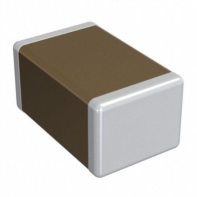
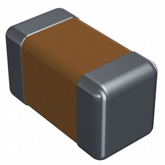
JMK107BJ475KAHT产品简介:
ICGOO电子元器件商城为您提供JMK107BJ475KAHT由TAIYO YUDEN-XENTEK设计生产,在icgoo商城现货销售,并且可以通过原厂、代理商等渠道进行代购。 JMK107BJ475KAHT价格参考¥0.15-¥0.15。TAIYO YUDEN-XENTEKJMK107BJ475KAHT封装/规格:陶瓷电容器, 4.7µF ±10% 6.3V 陶瓷电容器 X5R 0603(1608 公制)。您可以下载JMK107BJ475KAHT参考资料、Datasheet数据手册功能说明书,资料中有JMK107BJ475KAHT 详细功能的应用电路图电压和使用方法及教程。
Taiyo Yuden的JMK107BJ475KAHT是一款多层陶瓷电容器(MLCC),其主要参数包括容量为4.7μF,额定电压为50V,适用于多种电子设备和系统中。该型号电容器具有高可靠性、小尺寸和良好的温度稳定性,适合广泛应用场景。

常见应用场景包括:

1. 消费类电子产品:如智能手机、平板电脑、笔记本电脑和智能穿戴设备,用于电源去耦、滤波和信号稳定。

2. 汽车电子系统:如车载信息娱乐系统、ECU(电子控制单元)、传感器模块和ADAS(高级驾驶辅助系统),满足汽车环境对高稳定性和耐温性的要求。

3. 工业控制设备:如PLC(可编程逻辑控制器)、工业计算机、电机驱动器和自动化设备,用于电源管理与信号处理。

4. 通信设备:如基站、路由器、交换机和光模块,用于高频信号滤波与电源去耦,提升系统稳定性。

5. 电源管理模块:如DC-DC转换器、AC-DC电源适配器和电池管理系统,提供高效的能量存储与释放。

总之,JMK107BJ475KAHT凭借其优良性能,广泛应用于对可靠性与性能要求较高的电子系统中。
| 参数 | 数值 |
| 产品目录 | |
| 描述 | CAP CER 4.7UF 6.3V 10% X5R 0603多层陶瓷电容器MLCC - SMD/SMT X5R 0603 6.3V 4.7uF 10% |
| 产品分类 | |
| 品牌 | Taiyo Yuden |
| 产品手册 | http://www.yuden.co.jp/eu/product/category/capacitor/JMK107BJ475KAHT.html |
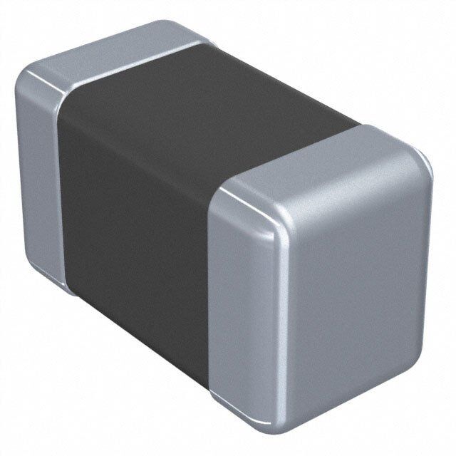
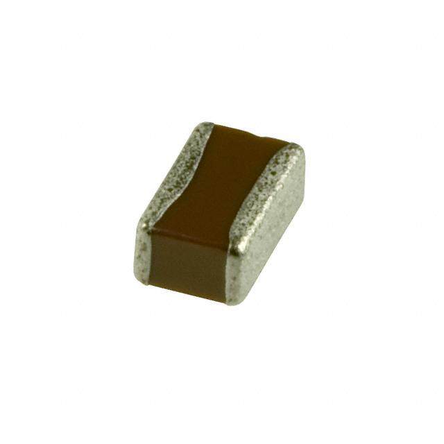
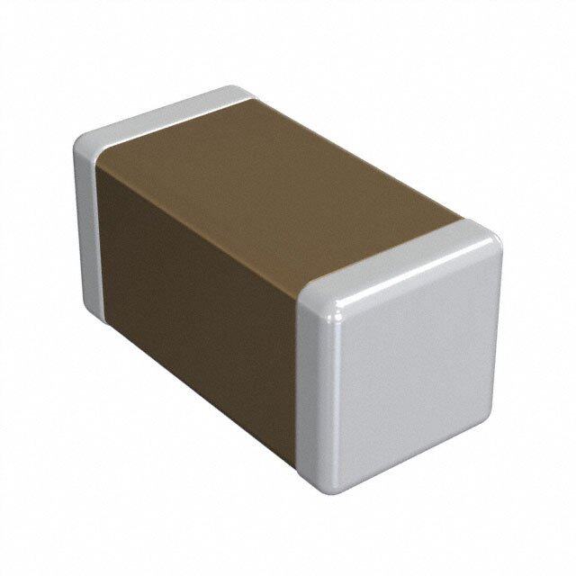
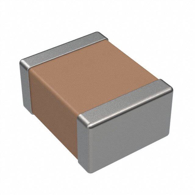
| 产品图片 |
|
| rohs | 符合RoHS无铅 / 符合限制有害物质指令(RoHS)规范要求 |
| 产品系列 | MLCC,多层陶瓷电容器MLCC - SMD/SMT,Taiyo Yuden JMK107BJ475KAHTM |
| 数据手册 | |
| 产品型号 | JMK107BJ475KAHT |
| 产品 | General Type MLCCs |
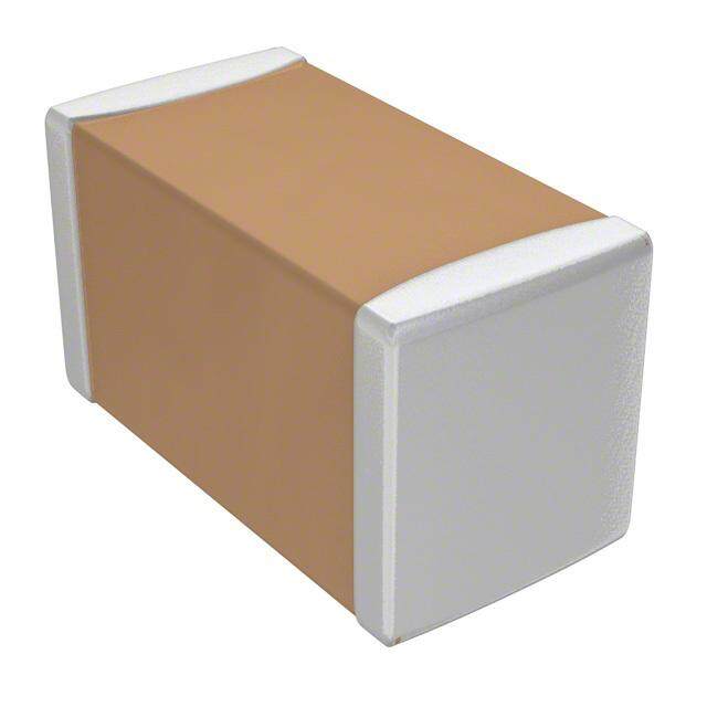
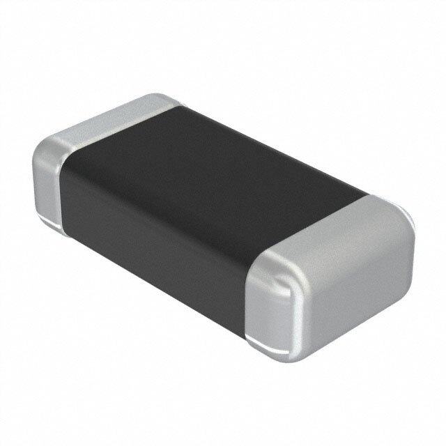
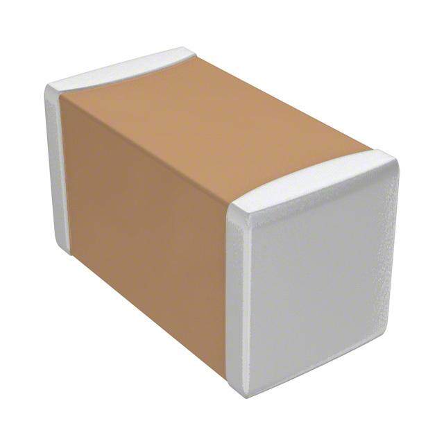
| 产品目录绘图 |
|
| 产品种类 | 多层陶瓷电容器MLCC - SMD/SMT |
| 其它名称 | 587-3387-1 |
| 包装 | 剪切带 (CT) |
| 厚度(最大值) | 0.035"(0.90mm) |
| 商标 | Taiyo Yuden |
| 外壳代码-in | 0603 |
| 外壳代码-mm | 1608 |
| 外壳宽度 | 0.8 mm |
| 外壳长度 | 1.6 mm |
| 外壳高度 | 0.8 mm |
| 大小/尺寸 | 0.063" 长 x 0.031" 宽(1.60mm x 0.80mm) |
| 安装类型 | 表面贴装,MLCC |
| 容差 | ±10% |
| 封装 | Reel |
| 封装/外壳 | 0603(1608 公制) |
| 封装/箱体 | 0603 (1608 metric) |
| 工作温度 | -55°C ~ 85°C |
| 工作温度范围 | - 55 C to + 85 C |
| 工厂包装数量 | 4000 |
| 应用 | 自动 |
| 引线形式 | - |
| 引线间距 | - |
| 最大工作温度 | + 85 C |
| 最小工作温度 | - 55 C |
| 标准包装 | 1 |
| 温度系数 | X5R |
| 温度系数/代码 | +/- 15 % |
| 特性 | - |
| 特色产品 | http://www.digikey.com/product-highlights/cn/zh/taiyo-yuden-multilayer-chip-capacitors/3897 |
| 电介质 | X5R |
| 电压-额定 | 6.3V |
| 电压额定值 | 6.3 V |
| 电压额定值DC | 6.3 V |
| 电容 | 4.7µF |
| 端接类型 | SMD/SMT |
| 等级 | AEC-Q200 |
| 类 | 2 |
| 类型 | Industrial/Automotive and Safety |
| 系列 | M |
| 零件号别名 | BJ475KAHT CE JMK107 |
| 高度-安装(最大值) | - |

.jpg)


- 商务部:美国ITC正式对集成电路等产品启动337调查
- 曝三星4nm工艺存在良率问题 高通将骁龙8 Gen1或转产台积电
- 太阳诱电将投资9.5亿元在常州建新厂生产MLCC 预计2023年完工
- 英特尔发布欧洲新工厂建设计划 深化IDM 2.0 战略
- 台积电先进制程称霸业界 有大客户加持明年业绩稳了
- 达到5530亿美元!SIA预计今年全球半导体销售额将创下新高
- 英特尔拟将自动驾驶子公司Mobileye上市 估值或超500亿美元
- 三星加码芯片和SET,合并消费电子和移动部门,撤换高东真等 CEO
- 三星电子宣布重大人事变动 还合并消费电子和移动部门
- 海关总署:前11个月进口集成电路产品价值2.52万亿元 增长14.8%


PDF Datasheet 数据手册内容提取
[ For High Quality and/or Reliability Equipment Notice for TAIYO YUDEN Products (Automotive Electronic Equipment / Industrial Equipment) ] Please read this notice before using the TAIYO YUDEN products. REMINDERS ■ Product information in this catalog is as of October 2018. All of the contents specified herein are subject to change without notice due to technical improvements, etc. Therefore, please check for the latest information carefully before practical application or use of our products. Please note that TAIYO YUDEN shall not be in any way responsible for any damages and defects in products or equipment incorporating our products, which are caused under the conditions other than those specified in this catalog or individual product specification sheets. ■ Please contact TAIYO YUDEN for further details of product specifications as the individual product specification sheets are available. ■ Please conduct validation and verification of our products in actual condition of mounting and operating environment before using our products. ■ The products listed in this catalog are intended for use in general electronic equipment (e.g., AV equipment, OA equipment, home electric appliances, office equipment, information and communication equipment), medical equipment classified as Class I or II by IMDRF, industrial equipment, and automotive interior applications, etc. Please be sure to contact TAIYO YUDEN for further information before using the products for any equipment which may directly cause loss of human life or bodily injury (e.g., transportation equipment including, without limitation, automotive powertrain control system, train control system, and ship control system, traffic signal equipment, medical equipment classified as Class III by IMDRF). Please do not incorporate our products into any equipment requiring high levels of safety and/or reliability (e.g., aerospace equipment, aviation equipment*, medical equipment classified as Class IV by IMDRF, nuclear control equipment, undersea equipment, military equipment). *Note: There is a possibility that our products can be used only for aviation equipment that does not directly affect the safe operation of aircraft (e.g., in-flight entertainment, cabin light, electric seat, cooking equipment) if such use meets requirements specified separately by TAIYO YUDEN. Please be sure to contact TAIYO YUDEN for further information before using our products for such aviation equipment. When our products are used even for high safety and/or reliability-required devices or circuits of general electronic equipment, it is strongly recommended to perform a thorough safety evaluation prior to use of our products and to install a protection circuit as necessary. Please note that unless you obtain prior written consent of TAIYO YUDEN, TAIYO YUDEN shall not be in any way responsible for any damages incurred by you or third parties arising from use of the products listed in this catalog for any equipment requiring inquiry to TAIYO YUDEN or prohibited for use by TAIYO YUDEN as described above. ■ Information contained in this catalog is intended to convey examples of typical performances and/or applications of our products and is not intended to make any warranty with respect to the intellectual property rights or any other related rights of TAIYO YUDEN or any third parties nor grant any license under such rights. ■ Please note that the scope of warranty for our products is limited to the delivered our products themselves and TAIYO YUDEN shall not be in any way responsible for any damages resulting from a fault or defect in our products. Notwithstanding the foregoing, if there is a written agreement (e.g., supply and purchase agreement, quality assurance agreement) signed by TAIYO YUDEN and your company, TAIYO YUDEN will warrant our products in accordance with such agreement. ■ The contents of this catalog are applicable to our products which are purchased from our sales offices or authorized distributors (hereinafter“ TAIYO YUDEN’s official sales channel”). Please note that the contents of this catalog are not applicable to our products purchased from any seller other than TAIYO YUDEN’s official sales channel. ■ Caution for Export Some of our products listed in this catalog may require specific procedures for export according to“ U.S. Export Administration Regulations”,“ Foreign Exchange and Foreign Trade Control Law” of Japan, and other applicable regulations. Should you have any questions on this matter, please contact our sales staff. 19
Automotive Application Guide We classify automotive electronic equipment into the following four application categories and set usable application categories for each of our products. When using our products for automotive electronic equipment, please be sure to check such application categories and use our products accordingly. Should you have any questions on this matter, please contact us. Category Automotive Electronic Equipment (Typical Example) ・Engine ECU (Electronically Controlled Fuel Injector) A ・Cruise Control Unit u t ・4WS (4 Wheel Steering) o m POWERTRAIN ・Automatic Transmission o t ・Power Steering iv e ・HEV/PHV/EV Core Control (Battery, Inverter, DC-DC) A ・Automotive Locator (Car location information providing device), etc. p p ・ABS (Anti-Lock Brake System) lic a ・ESC (Electronic Stability Control) t SAFETY io ・Airbag n ・ADAS (Equipment that directly controls running, turning and stopping), etc. G u ・Wiper id ・Automatic Door e ・Power Window ・Keyless Entry System BODY & CHASSIS ・Electric Door Mirror ・Interior Lighting ・LED Headlight ・TPMS (Tire Pressure Monitoring System) ・Anti-Theft Device (Immobilizer), etc. ・Car Infotainment System ・ITS/Telematics System INFOTAINMENT ・Instrument Cluster ・ADAS (Sensor, Equipment that is not interlocked with safety equipment or powertrain), etc. ▶ This catalog contains the typical specification only due to the limitation of space. When you consider the purchase of our products, please check our product specification sheets. For details of each product (characteristics graph, reliability information, precautions for use, and so on), see our website (http://www.ty-top.com/) . 19 15
MULTILAYER CERAMIC CAPACITORS MULTILAYER CERAMIC CAPACITORS REFLOW REFLOW A EACE-C Q-2Q02000 ■PART NUMBER J M K 3 1 6 △ B J 1 0 6 M L H T △ △=Blank space ① ② ③ ④ ⑤ ⑥ ⑦ ⑧ ⑨ ⑩ ⑪ ⑫ ①Rated voltage ③End termination Code Rated voltage[VDC] Code End termination A 4 K Plated J 6.3 J Soft Termination L 10 S Cu Internal Electrodes (For High Frequency) E 16 F High Reliability Application C E T 25 R G 35 ④Dimension(L×W) A U 50 Dimensions M Type EIA(inch) IC H 100 (L×W)[mm] Q 250 063 0.6 × 0.3 0201 C S 630 1.0 × 0.5 0402 A 105 P 0.52× 1.0 ※ 0204 A ②Series name 1.6 × 0.8 0603 C 107 IT Code Series name 0.8 × 1.6 ※ 0306 O M Multilayer ceramic capacitor 212 2.0 × 1.25 0805 R V Multilayer ceramic capacitor for high frequency 1.25× 2.0 ※ 0508 S W LW reverse type multilayer capacitor 316 3.2 × 1.6 1206 325 3.2 × 2.5 1210 432 4.5 × 3.2 1812 Note : ※LW reverse type(□WK) only ⑤Dimension tolerance Code Type L[mm] W[mm] T[mm] △ ALL Standard Standard Standard 063 0.6±0.05 0.3±0.05 0.3±0.05 105 1.0±0.10 0.5±0.10 0.5±0.10 107 1.6+0.15/-0.05 0.8+0.15/-0.05 0.8+0.15/-0.05 A 0.85±0.10 212 2.0+0.15/-0.05 1.25+0.15/-0.05 1.25+0.15/-0.05 316 3.2±0.20 1.6±0.20 1.6±0.20 325 3.2±0.30 2.5±0.30 2.5±0.30 105 1.0+0.15/-0.05 0.5+0.15/-0.05 0.5+0.15/-0.05 107 1.6+0.20/-0 0.8+0.20/-0 0.8+0.20/-0 B 0.85±0.10 212 2.0+0.20/-0 1.25+0.20/-0 1.25+0.20/-0 316 3.2±0.30 1.6±0.30 1.6±0.30 105 1.0+0.20/-0 0.5+0.20/-0 0.5+0.20/-0 C 107 1.6+0.25/-0 0.8+0.25/-0 0.8+0.25/-0 212 2.0+0.25/-0 1.25+0.25/-0 1.25+0.25/-0 212 2.0±0.15 1.25±0.15 0.85±0.15 1.15±0.20 K 316 3.2±0.20 1.6±0.20 1.6±0.20 325 3.2±0.50 2.5±0.30 2.5±0.30 Note: cf. STANDARD EXTERNAL DIMENSIONS △= Blank space ⑥Temperature characteristics code ■High dielectric type Applicable Temperature Capacitance Tolerance Code Ref. Temp.[℃] Capacitance change standard range[℃] tolerance code ±10% K BJ EIA X5R -55~+ 85 25 ±15% ±20% M ±10% K C6 EIA X6S -55~+105 25 ±22% ±20% M ±10% K B7 EIA X7R -55~+125 25 ±15% ±20% M ±10% K C7 EIA X7S -55~+125 25 ±22% ±20% M ±10% K D7 EIA X7T -55~+125 25 +22%/-33% ±20% M hq_c_mlcc_e-E07R01 ▶ This catalog contains the typical specification only due to the limitation of space. When you consider the purchase of our products, please check our product specification sheets. For details of each product (characteristics graph, reliability information, precautions for use, and so on), see our website (http://www.ty-top.com/) . 18 19
■Temperature compensating type Applicable Temperature Capacitance Tolerance Code Ref. Temp.[℃] Capacitance change standard range[℃] tolerance code ±0.1pF B JIS CG 20 ±0.25pF C ±0.5pF D CG -55~+125 0±30ppm/℃ ±1pF F EIA C0G 25 ±2% G ±5% J ⑦Nominal capacitance ⑨Thickness Code Code Thickness[mm] Nominal capacitance (example) P 0.3 0R5 0.5pF T 010 1pF V 0.5 100 10pF C 0.7(107type or more) 101 100pF A 0.8 102 1,000pF D 0.85(212type or more) C 103 0.01μF F 1.15 E R 104 0.1μF G 1.25 A 105 1.0μF L 1.6 M 106 10μF N 1.9 IC 107 100μF M 2.5 C Note : R=Decimal point A ⑩Special code P A ⑧Capacitance tolerance Code Special code C Code Capacitance tolerance H MLCC for Industrial and Automotive IT A ±0.05pF O B ±0.1pF ⑪Packaging R S C ±0.25pF Code Packaging D ±0.5pF F φ178mm Taping (2mm pitch) G ±2% R φ178mm Embossed Taping (4mm pitch) J ±5% T φ178mm Taping (4mm pitch) K ±10% φ178mm Taping (4mm pitch, 1000 pcs/reel) P M ±20% 325 type(Thickness code M) ⑫Internal code Code Internal code △ Standard hq_c_mlcc_e-E07R01 ▶ This catalog contains the typical specification only due to the limitation of space. When you consider the purchase of our products, please check our product specification sheets. For details of each product (characteristics graph, reliability information, precautions for use, and so on), see our website (http://www.ty-top.com/) . 19 19
■STANDARD EXTERNAL DIMENSIONS W Dimension [mm] (inch) Type( EIA ) L L W T *1 e 0.6±0.03 0.3±0.03 0.3±0.03 0.15±0.05 □MK063(0201) T T (0.024±0.001) (0.012±0.001) (0.012±0.001) (0.006±0.002) □MK105(0402) 1.0±0.05 0.5±0.05 0.5±0.05 0.25±0.10 V e □MF105(0402) (0.039±0.002) (0.020±0.002) (0.020±0.002) (0.010±0.004) 0.52±0.05 1.0±0.05 0.3±0.05 0.18±0.08 □WK105(0204)※ P (0.020±0.002) (0.039±0.002) (0.012±0.002) (0.007±0.003) □MK107(0603) 1.6±0.10 0.8±0.10 0.8±0.10 0.35±0.25 A □MF107(0603) (0.063±0.004) (0.031±0.004) (0.031±0.004) (0.014±0.010) L 1.6±0.10 0.8±0.10 0.8±0.10 0.35+0.3/-0.25 □MJ107(0603) A (0.063±0.004) (0.031±0.004) (0.031±0.004) (0.014+0.012/-0.010) W 1.6±0.10 0.8±0.10 0.7±0.10 0.35±0.25 □VS107(0603) C (0.063±0.004) (0.031±0.004) (0.028±0.004) (0.014±0.010) 0.8±0.10 1.6±0.10 0.5±0.05 0.25±0.15 □WK107(0306)※ V C (0.031±0.004) (0.063±0.004) (0.020±0.002) (0.010±0.006) E T 0.85±0.10 R D A □MK212(0805) 2.0±0.10 1.25±0.10 (0.033±0.004) 0.5±0.25 M e □MF212(0805) (0.079±0.004) (0.049±0.004) 1.25±0.10 (0.020±0.010) IC (0.049±0.004) G ※ LW reverse type C 0.85±0.10 D A 2.0±0.10 1.25±0.10 (0.033±0.004) 0.5+0.35/-0.25 □MJ212(0805) P (0.079±0.004) (0.049±0.004) 1.25±0.10 (0.020+0.014/-0.010) A G C (0.049±0.004) IT 2.0±0.10 1.25±0.10 0.85±0.10 0.5±0.25 □VS212(0805) D O (0.079±0.004) (0.049±0.004) (0.033±0.004) (0.020±0.010) R 1.25±0.15 2.0±0.15 0.85±0.10 0.3±0.2 S □WK212(0508)※ D (0.049±0.006) (0.079±0.006) (0.033±0.004) (0.012±0.008) 1.15±0.10 F □MK316(1206) 3.2±0.15 1.6±0.15 (0.045±0.004) 0.5+0.35/-0.25 □MF316(1206) (0.126±0.006) (0.063±0.006) 1.6±0.20 (0.020+0.014/-0.010) L (0.063±0.008) 1.15±0.10 F 3.2±0.15 1.6±0.15 (0.045±0.004) 0.6+0.4/-0.3 □MJ316(1206) (0.126±0.006) (0.063±0.006) 1.6±0.20 (0.024+0.016/-0.012) L (0.063±0.008) 1.15±0.10 F (0.045±0.004) □MK325(1210) 3.2±0.30 2.5±0.20 1.9±0.20 0.6±0.3 N □MF325(1210) (0.126±0.012) (0.098±0.008) (0.075±0.008) (0.024±0.012) 2.5±0.20 M (0.098±0.008) 1.9±0.20 N 3.2±0.30 2.5±0.20 (0.075±0.008) 0.6+0.4/-0.3 □MJ325(1210) (0.126±0.012) (0.098±0.008) 2.5±0.20 (0.024+0.016/-0.012) M (0.098±0.008) 4.5±0.40 3.2±0.30 2.5±0.20 0.9±0.6 □MK432(1812) M (0.177±0.016) (0.126±0.012) (0.098±0.008) (0.035±0.024) Note : ※. LW reverse type, *1.Thickness code hq_c_mlcc_e-E07R01 ▶ This catalog contains the typical specification only due to the limitation of space. When you consider the purchase of our products, please check our product specification sheets. For details of each product (characteristics graph, reliability information, precautions for use, and so on), see our website (http://www.ty-top.com/) . 20 19
■STANDARD QUANTITY Dimension Standard quantity[pcs] Type EIA(inch) [mm] Code Paper tape Embossed tape 063 0201 0.3 T 15000 - 0402 0.5 V 105 10000 - 0204 ※ 0.30 P 0.7 C 4000 - 0.8 A 3000 0603 0.8 A - 107 (Soft Termination) 3000 0.8 A - (Soft Termination) 0306 ※ 0.50 V - 4000 0.85 D 4000 - 1.25 G - 3000 0805 212 2000 1.25 G - (Soft Termination) C 0508 ※ 0.85 D 4000 - E 1.15 F - 3000 R 316 1206 1.6 L - 2000 A M 1.15 F 325 1210 1.9 N - 2000 IC 2.5 M - 500(T),1000(P) C 432 1812 2.5 M - 500 A P Note : ※.LW Reverse type(□WK) A C IT O R S hq_c_mlcc_e-E07R01 ▶ This catalog contains the typical specification only due to the limitation of space. When you consider the purchase of our products, please check our product specification sheets. For details of each product (characteristics graph, reliability information, precautions for use, and so on), see our website (http://www.ty-top.com/) . 19 21
■PART NUMBER Soft Termination Multilayer Ceramic Capacitors ●107TYPE (Dimension:1.6×0.8mm JIS:1608 EIA:0603) 【Temperature Characteristic B7 : X7R(-55~+125℃)】 0.8mm thickness(A) Part number 1 Part number 2 Rated[ Vv]oltage cThaermapceteraritsutrices Capa c[Fit]ance toClaepraanccitea n[c%e] t a[%nδ] Rated vHoTltLaTge x % Thickness*3 [mm] Note TMJ107BB7473[]AHT X7R 0.047μ ±10, ±20 3.5 200 0.8+0.20/-0 *1, *2 TMJ107BB7104[]AHT X7R 0.1μ ±10, ±20 3.5 200 0.8+0.20/-0 *1, *2 TMJ107BB7224[]AHT 25 X7R 0.22μ ±10, ±20 10 150 0.8+0.20/-0 *1, *2 TMJ107BB7474[]AHT X7R 0.47μ ±10, ±20 10 150 0.8+0.20/-0 *1, *2 TMJ107CB7105[]AHR X7R 1μ ±10, ±20 10 150 0.8+0.25/-0 *1, *2 GMJ107BB7473[]AHT X7R 0.047μ ±10, ±20 3.5 200 0.8+0.20/-0 *1, *2 GMJ107BB7104[]AHT X7R 0.1μ ±10, ±20 3.5 200 0.8+0.20/-0 *1, *2 GMJ107BB7224[]AHT 35 X7R 0.22μ ±10, ±20 10 150 0.8+0.20/-0 *1, *2 GMJ107BB7474[]AHT X7R 0.47μ ±10, ±20 10 150 0.8+0.20/-0 *1, *2 GMJ107CB7105[]AHR X7R 1μ ±10, ±20 10 150 0.8+0.25/-0 *1, *2 UMJ107AB7102[]AHT X7R 1000p ±10, ±20 3.5 200 0.8+0.15/-0.05 *1, *2 UMJ107AB7222[]AHT X7R 2200p ±10, ±20 3.5 200 0.8+0.15/-0.05 *1, *2 UMJ107BB7472[]AHT X7R 4700p ±10, ±20 3.5 200 0.8+0.20/-0 *1, *2 UMJ107BB7103[]AHT 50 X7R 0.01μ ±10, ±20 3.5 200 0.8+0.20/-0 *1, *2 C UMJ107BB7223[]AHT X7R 0.022μ ±10, ±20 3.5 200 0.8+0.20/-0 *1, *2 E R UMJ107BB7473[]AHT X7R 0.047μ ±10, ±20 3.5 200 0.8+0.20/-0 *1, *2 A UMJ107BB7104[]AHT X7R 0.1μ ±10, ±20 3.5 200 0.8+0.20/-0 *1, *2 M HMJ107AB7102[]AHT X7R 1000p ±10, ±20 3.5 200 0.8+0.15/-0.05 *1, *2 HMJ107AB7222[]AHT X7R 2200p ±10, ±20 3.5 200 0.8+0.15/-0.05 *1, *2 IC HMJ107BB7472[]AHT X7R 4700p ±10, ±20 3.5 200 0.8+0.20/-0 *1, *2 C HMJ107BB7103[]AHT 100 X7R 0.01μ ±10, ±20 3.5 200 0.8+0.20/-0 *1, *2 A HMJ107BB7223[]AHT X7R 0.022μ ±10, ±20 3.5 200 0.8+0.20/-0 *1, *2 P HMJ107BB7473[]AHT X7R 0.047μ ±10, ±20 3.5 200 0.8+0.20/-0 *1, *2 A HMJ107BB7104[]AHT X7R 0.1μ ±10, ±20 3.5 200 0.8+0.20/-0 *1, *2 C IT O ●212TYPE (Dimension:2.0×1.25mm JIS:2012 EIA:0805) R 【Temperature Characteristic B7 : X7R(-55~+125℃), C7 : X7S(-55~+125℃)】 0.85mm thickness(D)、1.25mm thickness(G) S Part number 1 Part number 2 Rated[ Vv]oltage cThaermapceteraritsutrices Capa c[Fit]ance toClaepraanccitea n[c%e] t a[%nδ] Rated vHoTltLaTge x % Thickness*3 [mm] Note JMJ212CB7106[]GHT 6.3 X7R 10μ ±10, ±20 10 150 1.25+0.25/-0 *1, *2 EMJ212CB7225[]GHT X7R 2.2μ ±10, ±20 10 150 1.25+0.25/-0 *1, *2 16 EMJ212CB7475[]GHT X7R 4.7μ ±10, ±20 10 150 1.25+0.25/-0 *1, *2 TMJ212CB7225[]GHT 25 X7R 2.2μ ±10, ±20 10 150 1.25+0.25/-0 *1, *2 GMJ212CB7105[]GHT 35 X7R 1μ ±10, ±20 10 150 1.25+0.25/-0 *1, *2 UMJ212BB7103[]GHT X7R 0.01μ ±10, ±20 3.5 200 1.25+0.20/-0 *1, *2 UMJ212BB7223[]GHT X7R 0.022μ ±10, ±20 3.5 200 1.25+0.20/-0 *1, *2 UMJ212BB7473[]GHT X7R 0.047μ ±10, ±20 3.5 200 1.25+0.20/-0 *1, *2 UMJ212BB7104[]GHT 50 X7R 0.1μ ±10, ±20 3.5 200 1.25+0.20/-0 *1, *2 UMJ212BB7224[]GHT X7R 0.22μ ±10, ±20 3.5 200 1.25+0.20/-0 *1, *2 UMJ212CC7474[]GHTE X7S 0.47μ ±10, ±20 3.5 150 1.25+0.25/-0 *1, *2 UMJ212CB7105[]GHT X7R 1μ ±10, ±20 10 150 1.25+0.25/-0 *1, *2 HMJ212KB7102[]DHT X7R 1000p ±10, ±20 3.5 200 0.85±0.15 *1, *2 HMJ212KB7222[]DHT X7R 2200p ±10, ±20 3.5 200 0.85±0.15 *1, *2 HMJ212BB7472[]GHT X7R 4700p ±10, ±20 3.5 200 1.25+0.20/-0 *1, *2 HMJ212BB7103[]GHT X7R 0.01μ ±10, ±20 3.5 200 1.25+0.20/-0 *1, *2 HMJ212BB7223[]GHT 100 X7R 0.022μ ±10, ±20 3.5 200 1.25+0.20/-0 *1, *2 HMJ212BB7473[]GHT X7R 0.047μ ±10, ±20 3.5 200 1.25+0.20/-0 *1, *2 HMJ212BB7104[]GHT X7R 0.1μ ±10, ±20 3.5 200 1.25+0.20/-0 *1, *2 HMJ212BB7224[]GHT X7R 0.22μ ±10, ±20 3.5 200 1.25+0.20/-0 *1, *2 HMJ212CC7474[]GHTE X7S 0.47μ ±10, ±20 3.5 150 1.25+0.25/-0 *1, *2 QMJ212KB7102[]DHT X7R 1000p ±10, ±20 2.5 150 0.85±0.15 *1, *2 QMJ212KB7222[]DHT X7R 2200p ±10, ±20 2.5 150 0.85±0.15 *1, *2 QMJ212BB7472[]GHT 250 X7R 4700p ±10, ±20 2.5 150 1.25+0.20/-0 *1, *2 QMJ212BB7103[]GHT X7R 0.01μ ±10, ±20 2.5 150 1.25+0.20/-0 *1, *2 QMJ212BB7223[]GHT X7R 0.022μ ±10, ±20 2.5 150 1.25+0.20/-0 *1, *2 hq_c_mlcc_e-E07R01 ▶ This catalog contains the typical specification only due to the limitation of space. When you consider the purchase of our products, please check our product specification sheets. For details of each product (characteristics graph, reliability information, precautions for use, and so on), see our website (http://www.ty-top.com/) . 19 33
■PART NUMBER ●316TYPE (Dimension:3.2×1.6mm JIS:3216 EIA:1206) 【Temperature Characteristic B7 : X7R(-55~+125℃), C7 : X7S(-55~+125℃)】 1.15mm thickness(F)、1.6mm thickness(L) Part number 1 Part number 2 Rated[ Vv]oltage cThaermapceteraritsutrices Capa c[Fit]ance toClaepraanccitea n[c%e] t a[%nδ] Rated vHoTltLaTge x % Thickness*3 [mm] Note LMJ316BB7226[]LHT 10 X7R 22μ ±10, ±20 10 150 1.6±0.30 *1, *2 EMJ316BB7475[]LHT X7R 4.7μ ±10, ±20 10 150 1.6±0.30 *1, *2 16 EMJ316BB7106[]LHT X7R 10μ ±10, ±20 10 150 1.6±0.30 *1, *2 TMJ316BB7474[]LHT X7R 0.47μ ±10, ±20 3.5 200 1.6±0.30 *1, *2 TMJ316BB7475[]LHT 25 X7R 4.7μ ±10, ±20 10 150 1.6±0.30 *1, *2 TMJ316BB7106[]LHT X7R 10μ ±10, ±20 10 150 1.6±0.30 *1, *2 GMJ316BB7474[]LHT X7R 0.47μ ±10, ±20 3.5 200 1.6±0.30 *1, *2 GMJ316AB7225[]LHT X7R 2.2μ ±10, ±20 10 150 1.6±0.20 *1, *2 35 GMJ316BB7475[]LHT X7R 4.7μ ±10, ±20 10 150 1.6±0.30 *1, *2 GMJ316BB7106[]LHT X7R 10μ ±10, ±20 10 150 1.6±0.30 *1, *2 UMJ316BB7473[]LHT X7R 0.047μ ±10, ±20 3.5 200 1.6±0.30 *1, *2 UMJ316BB7104[]LHT X7R 0.1μ ±10, ±20 3.5 200 1.6±0.30 *1, *2 UMJ316BB7224[]LHT X7R 0.22μ ±10, ±20 3.5 200 1.6±0.30 *1, *2 UMJ316BB7474[]LHT 50 X7R 0.47μ ±10, ±20 3.5 200 1.6±0.30 *1, *2 UMJ316BB7105[]LHT X7R 1μ ±10, ±20 3.5 200 1.6±0.30 *1, *2 C UMJ316AB7225[]LHT X7R 2.2μ ±10, ±20 10 150 1.6±0.20 *1, *2 E UMJ316BC7475[]LHTE X7S 4.7μ ±10, ±20 2.5 150 1.6±0.30 *1, *2 R HMJ316 B7102[]FHT X7R 1000p ±10, ±20 3.5 200 1.15±0.10 *1, *2 A HMJ316 B7222[]FHT X7R 2200p ±10, ±20 3.5 200 1.15±0.10 *1, *2 M HMJ316 B7472[]FHT X7R 4700p ±10, ±20 3.5 200 1.15±0.10 *1, *2 IC HMJ316KB7103[]FHT X7R 0.01μ ±10, ±20 3.5 200 1.15±0.20 *1, *2 HMJ316BB7223[]LHT X7R 0.022μ ±10, ±20 3.5 200 1.6±0.30 *1, *2 C HMJ316BB7473[]LHT 100 X7R 0.047μ ±10, ±20 3.5 200 1.6±0.30 *1, *2 A HMJ316BB7104[]LHT X7R 0.1μ ±10, ±20 3.5 200 1.6±0.30 *1, *2 P HMJ316BB7224[]LHT X7R 0.22μ ±10, ±20 3.5 200 1.6±0.30 *1, *2 A HMJ316BB7474[]LHT X7R 0.47μ ±10, ±20 3.5 200 1.6±0.30 *1, *2 C HMJ316BB7105[]LHT X7R 1μ ±10, ±20 3.5 200 1.6±0.30 *1, *2 IT HMJ316BC7225[]LHTE X7S 2.2μ ±10, ±20 3.5 150 1.6±0.30 *1, *2 O QMJ316 B7102[]FHT X7R 1000p ±10, ±20 2.5 150 1.15±0.10 *1, *2 R QMJ316 B7222[]FHT X7R 2200p ±10, ±20 2.5 150 1.15±0.10 *1, *2 S QMJ316 B7472[]FHT X7R 4700p ±10, ±20 2.5 150 1.15±0.10 *1, *2 QMJ316KB7103[]FHT 250 X7R 0.01μ ±10, ±20 2.5 150 1.15±0.20 *1, *2 QMJ316BB7223[]LHT X7R 0.022μ ±10, ±20 2.5 150 1.6±0.30 *1, *2 QMJ316BB7473[]LHT X7R 0.047μ ±10, ±20 2.5 150 1.6±0.30 *1, *2 QMJ316BB7104[]LHT X7R 0.1μ ±10, ±20 2.5 150 1.6±0.30 *1, *2 SMJ316 B7102[]FHT X7R 1000p ±10, ±20 2.5 120 1.15±0.10 *1, *2 SMJ316 B7222[]FHT X7R 2200p ±10, ±20 2.5 120 1.15±0.10 *1, *2 SMJ316 B7472[]FHT 630 X7R 4700p ±10, ±20 2.5 120 1.15±0.10 *1, *2 SMJ316KB7103[]FHT X7R 0.01μ ±10, ±20 2.5 120 1.15±0.20 *1, *2 SMJ316BB7223[]LHT X7R 0.022μ ±10, ±20 2.5 120 1.6±0.30 *1, *2 ●325TYPE (Dimension:3.2×2.5mm JIS:3225 EIA:1210) 【Temperature Characteristic B7 : X7R(-55~+125℃), C7 : X7S(-55~+125℃)】 1.9mm thickness(N)、2.5mm thickness(M) Part number 1 Part number 2 Rated[ Vv]oltage cThaermapceteraritsutrices Capa c[Fit]ance toClaepraanccitea n[c%e] t a[%nδ] Rated vHoTltLaTge x % Thickness*3 [mm] Note JMJ325KB7476[]MHP 6.3 X7R 47μ ±10, ±20 10 150 2.5±0.30 *1, *2 EMJ325KB7226[]MHP 16 X7R 22μ ±10, ±20 10 150 2.5±0.30 *1, *2 TMJ325AB7475[]MHP X7R 4.7μ ±10, ±20 5 150 2.5±0.30 *1, *2 25 TMJ325KB7106[]MHP X7R 10μ ±10, ±20 10 150 2.5±0.30 *1, *2 GMJ325AB7475[]MHP X7R 4.7μ ±10, ±20 5 150 2.5±0.30 *1, *2 35 GMJ325KB7106[]MHP X7R 10μ ±10, ±20 10 150 2.5±0.30 *1, *2 UMJ325AB7225[]MHP X7R 2.2μ ±10, ±20 3.5 200 2.5±0.30 *1, *2 UMJ325AB7475[]MHP 50 X7R 4.7μ ±10, ±20 5 150 2.5±0.30 *1, *2 UMJ325KB7106[]MHP X7R 10μ ±10, ±20 10 150 2.5±0.30 *1, *2 HMJ325 B7223[]NHT X7R 0.022μ ±10, ±20 3.5 200 1.9±0.20 *1, *2 HMJ325 B7473[]NHT X7R 0.047μ ±10, ±20 3.5 200 1.9±0.20 *1, *2 HMJ325 B7104[]NHT X7R 0.1μ ±10, ±20 3.5 200 1.9±0.20 *1, *2 HMJ325 B7224[]NHT X7R 0.22μ ±10, ±20 3.5 200 1.9±0.20 *1, *2 100 HMJ325 B7474[]NHT X7R 0.47μ ±10, ±20 3.5 200 1.9±0.20 *1, *2 HMJ325 B7105[]NHT X7R 1μ ±10, ±20 3.5 200 1.9±0.20 *1, *2 HMJ325AB7225[]MHP X7R 2.2μ ±10, ±20 3.5 200 2.5±0.30 *1, *2 HMJ325KC7475[]MHPE X7S 4.7μ ±10, ±20 3.5 150 2.5±0.30 *1, *2 QMJ325 B7223[]NHT X7R 0.022μ ±10, ±20 2.5 150 1.9±0.20 *1, *2 QMJ325 B7473[]NHT X7R 0.047μ ±10, ±20 2.5 150 1.9±0.20 *1, *2 250 QMJ325 B7104[]NHT X7R 0.1μ ±10, ±20 2.5 150 1.9±0.20 *1, *2 QMJ325 B7224[]NHT X7R 0.22μ ±10, ±20 2.5 150 1.9±0.20 *1, *2 SMJ325 B7223[]NHT X7R 0.022μ ±10, ±20 2.5 120 1.9±0.20 *1, *2 630 SMJ325 B7473[]NHT X7R 0.047μ ±10, ±20 2.5 120 1.9±0.20 *1, *2 hq_c_mlcc_e-E07R01 ▶ This catalog contains the typical specification only due to the limitation of space. When you consider the purchase of our products, please check our product specification sheets. For details of each product (characteristics graph, reliability information, precautions for use, and so on), see our website (http://www.ty-top.com/) . 34 19
Multilayer Ceramic Capacitors ■PACKAGING ①Minimum Quantity ●Taped package Thickness Standard quantity [pcs] Type(EIA) mm code Paper tape Embossed tape □MK021(008004) 0.125 K - 50000 □VS021(008004) □MK042(01005) 0.2 C, D - 40000 □VS042(01005) 0.2 C □MK063(0201) 0.3 P,T 15000 - □WK105(0204) ※ 0.3 P 10000 - 0.13 H - 20000 0.18 E - 15000 □MK105(0402) 0.2 C 20000 - □MF105(0402) 0.3 P 15000 - 0.5 V 10000 - □VK105(0402) 0.5 W 10000 - □MK107(0603) 0.45 K 4000 - □WK107(0306) ※ 0.5 V - 4000 □MF107(0603) 0.8 A 4000 - □VS107(0603) 0.7 C 4000 - □MJ107(0603) 0.8 A 3000 3000 □MK212(0805) 0.45 K 4000 - □WK212(0508) ※ 0.85 D □MF212(0805) 1.25 G - 3000 □VS212(0805) 0.85 D 4000 - 0.85 D 4000 - □MJ212(0805) 1.25 G - 2000 0.85 D 4000 - □MK316(1206) 1.15 F - 3000 □MF316(1206) 1.6 L - 2000 1.15 F - 3000 □MJ316(1206) 1.6 L - 2000 0.85 D 1.15 F □MK325(1210) - 2000 1.9 N □MF325(1210) 2.0max. Y 2.5 M - 1000 1.9 N - 2000 □MJ325(1210) 2.5 M - 500(T), 1000(P) □MK432(1812) 2.5 M - 500 Note : ※ LW Reverse type. ②Taping material ※No bottom tape for pressed carrier tape ●Card board carrier tape ●Embossed tape Top tape Top tape Base tape Sprocket hole Sprocket hole Bottom tape Chip cavity Base tape Chip cavity ▶ This catalog contains the typical specification only due to the limitation of space. When you consider the purchase of our products, please check our specification. For details of each product (characteristics graph, reliability information, precautions for use, and so on), see our Web site (http://www.ty-top.com/) . c_mlcc_pack_e-E06R01
Chip filled Chip ※ LW Reverse type. ③Representative taping dimensions ●Paper Tape(8mm wide) ●Pressed carrier tape( 2mm pitch) Unit:mm(inch) φ1.5+0.1/-0 1.75±0.1 Sprockethole (φ0.059+0.004/-0) (0.069±0.004) T A B 3.5±0.05(0.138±0.002) 8.0±0.30.315±0.012) ( T1 F 2.0±0.05 4.0±0.1 (0.079±0.002) (0.157±0.004) Chip Cavity Insertion Pitch Tape Thickness Type(EIA) A B F T T1 □MK063(0201) 0.37 0.67 0.45max. 0.42max. □WK105(0204) ※ 2.0±0.05 □MK105(0402) (*1 C) 0.65 1.15 0.4max. 0.3max. □MK105(0402) (*1 P) 0.45max. 0.42max. Note *1 Thickness, C:0.2mm ,P:0.3mm. ※ LW Reverse type. Unit:mm ●Punched carrier tape (2mm pitch) Unit:mm(inch) φ1.5+0.1/-0 1.75±0.1 Sprockethole (φ0.059+0.004/-0) (0.069±0.004) T A B 3.5±0.05(0.138±0.002) 8.0±0.30.315±0.012) ( F 2.0±0.05 4.0±0.1 (0.079±0.002) (0.157±0.004) Chip Cavity Insertion Pitch Tape Thickness Type(EIA) A B F T □MK105 (0402) □MF105 (0402) 0.65 1.15 2.0±0.05 0.8max. □VK105 (0402) Unit:mm ●Punched carrier tape (4mm pitch) Unit:mm(inch) φ1.5+0.1/-0 1.75±0.1 Sprockethole (φ0.059+0.004/-0) (0.069±0.004) T A B 3.5±0.050.138±0.002) 8.0±0.3315±0.012) ( 0. ( F 4.0±0.1 (0.157±0.004) 2.0±0.1 (0.079±0.004) ▶ This catalog contains the typical specification only due to the limitation of space. When you consider the purchase of our products, please check our specification. For details of each product (characteristics graph, reliability information, precautions for use, and so on), see our Web site (http://www.ty-top.com/) . c_mlcc_pack_e-E06R01
Chip Cavity Insertion Pitch Tape Thickness Type(EIA) A B F T □MK107(0603) □WK107(0306) ※ 1.0 1.8 1.1max. □MF107(0603) 4.0±0.1 □MK212(0805) 1.65 2.4 □WK212(0508) ※ 1.1max. □MK316(1206) 2.0 3.6 Note:Taping size might be different depending on the size of the product. ※ LW Reverse type. Unit:mm ●Embossed tape(4mm wide) Unit:mm(inch) φ0.8±0.04 0.9±0.05 Sprockethole (φ0.031±0.002) (0.035±0.002) A B 1.8±0.02(0.071±0.001) 4.0±0.050.157±0.002) ( F 1.0±0.02 2.0±0.04 (0.039±0.001) (0.079±0.002) Chip Cavity Insertion Pitch Tape Thickness Type(EIA) A B F K T □MK021(008004) 0.135 0.27 □VS021(008004) 1.0±0.02 0.5max. 0.25max. □MK042(01005) 0.23 0.43 □VS042(01005) Unit:mm ●Embossed tape(8mm wide) Unit:mm(inch) φ1.5+0.1/-0 1.75±0.1 Sprockethole (φ0.059+0.004/-0) (0.069±0.004) A B 3.5±0.050.138±0.002) 8.0±0.3315±0.012) ( 0. ( F 4.0±0.1 (0.157±0.004) 2.0±0.1 (0.079±0.004) Chip Cavity Insertion Pitch Tape Thickness Type(EIA) A B F K T □MK105(0402) 0.6 1.1 2.0±0.1 0.6max 0.2±0.1 □WK107(0306) ※ 1.0 1.8 1.3max. 0.25±0.1 □MK212(0805) 1.65 2.4 □MF212(0805) □MK316(1206) 4.0±0.1 2.0 3.6 3.4max. 0.6max. □MF316(1206) □MK325(1210) 2.8 3.6 □MF325(1210) Note: ※ LW Reverse type. Unit:mm ▶ This catalog contains the typical specification only due to the limitation of space. When you consider the purchase of our products, please check our specification. For details of each product (characteristics graph, reliability information, precautions for use, and so on), see our Web site (http://www.ty-top.com/) . c_mlcc_pack_e-E06R01
●Embossed tape(12mm wide) Unit:mm(inch) φ1.5+0.1/-0 1.75±0.1 Sprockethole (φ0.059+0.004/-0) (0.069±0.004) B A 5.5±0.050.217±0.002) 12.0±0.3472±0.012) ( 0. ( 4.0±0.1 2.0±0.1 (0.157±0.004) (0.079±0.004) F Chip Cavity Insertion Pitch Tape Thickness Type(EIA) A B F K T □MK325(1210) 3.1 4.0 8.0±0.1 4.0max. 0.6max. □MK432(1812) 3.7 4.9 8.0±0.1 4.0max. 0.6max. Unit:mm ④Trailer and Leader Blank portion Chip cavity Blank portion Leader 160mm or more 100mm or more (6.3inches or more) (3.94inches or more) 400mm or more Direction of tape feed (15.7inches or more) ⑤Reel size t E C B A R D W A B C D E R φ178±2.0 φ50min. φ13.0±0.2 φ21.0±0.8 2.0±0.5 1.0 T W 4mm wide tape 1.5max. 5±1.0 8mm wide tape 2.5max. 10±1.5 12mm wide tape 2.5max. 14±1.5 Unit:mm ⑥Top Tape Strength The top tape requires a peel-off force of 0.1 to 0.7N in the direction of the arrow as illustrated below. Pull direction 0~20° Top tape Base tape ▶ This catalog contains the typical specification only due to the limitation of space. When you consider the purchase of our products, please check our specification. For details of each product (characteristics graph, reliability information, precautions for use, and so on), see our Web site (http://www.ty-top.com/) . c_mlcc_pack_e-E06R01
Multilayer Ceramic Capacitors ■RELIABILITY DATA 1.Operating Temperature Range Temperature Standard -55 to +125℃ Compensating(Class1) High Frequency Type Specification Temperature Range B -25 to +85℃ BJ Specified X5R -55 to +85℃ Value B7 X7R -55 to +125℃ High Permittivity (Class2) C6 X6S -55 to +105℃ C7 X7S -55 to +125℃ D7 X7T -55 to +125℃ LD(※) X5R -55 to +85℃ Note: ※LD Low distortion high value multilayer ceramic capacitor 2. Storage Conditions Temperature Standard -55 to +125℃ Compensating(Class1) High Frequency Type Specification Temperature Range B -25 to +85℃ BJ Specified X5R -55 to +85℃ Value B7 X7R -55 to +125℃ High Permittivity (Class2) C6 X6S -55 to +105℃ C7 X7S -55 to +125℃ D7 X7T -55 to +125℃ LD(※) X5R -55 to +85℃ Note: ※LD Low distortion high value multilayer ceramic capacitor 3. Rated Voltage Temperature Standard 50VDC, 25VDC Specified Compensating(Class1) High Frequency Type 50VDC, 25VDC Value High Permittivity (Class2) 50VDC, 35VDC, 25VDC, 16VDC, 10VDC, 6.3VDC, 4VDC, 2.5VDC 4. Withstanding Voltage (Between terminals) Temperature Standard Specified Compensating(Class1) High Frequency Type No breakdown or damage Value High Permittivity (Class2) Class 1 Class 2 Test Applied voltage Rated volta×3 Rated voltage×2.5 Methods and Duration 1 to 5 sec. Remarks Charge/discharge current 50mA max. 5. Insulation Resistance Temperature Standard 10000 MΩ min. Specified Compensating(Class1) High Frequency Type Value C≦0.047μF : 10000 MΩ min. High Permittivity (Class2) Note 1 C>0.047μF : 500MΩ・μF Test Applied voltage : Rated voltage Methods and Duration : 60±5 sec. Remarks Charge/discharge current : 50mA max. ▶ This catalog contains the typical specification only due to the limitation of space. When you consider the purchase of our products, please check our specification. For details of each product (characteristics graph, reliability information, precautions for use, and so on), see our Web site (http://www.ty-top.com/) . hq_c_mlcc_reli_e-E06R01
6. Capacitance (Tolerance) C□ 0.2pF≦C≦5pF : ±0.25pF Standard U□ 0.2pF≦C≦10pF : ±0.5pF Temperature SL C>10pF : ±5% or ±10% Specified Compensating(Class1) 0.3pF≦C≦2pF : ±0.1pF Value High Frequency Type CH C>2pF : ±5% BJ, B7, C6, C7, D7, LD(※) : ±10% or ±20% High Permittivity (Class2) Note: ※LD Low distortion high value multilayer ceramic capacitor Class 1 Class 2 Standard High Frequency Type C≦10μF C>10μF Test Preconditioning None Thermal treatment (at 150℃ for 1hr) Note 2 Methods and Measuring frequency 1MHz±10% 1kHz±10% 120±10Hz Remarks Measuring voltage Note 0.5 to 5Vrms 1±0.2Vrms 0.5±0.1rms Bias application one 7. Q or Dissipation Factor C<30pF : Q≧400+20C Temperature Standard C≧30pF : Q≧1000 (C:Nominal capacitance) Specified Compensating(Class1) Value High Frequency Type Refer to detailed specification High Permittivity (Class2) Note 1 BJ, B7, C6, C7, D7:2.5% max. Class 1 Class 2 Standard High Frequency Type C≦10μF C>10μF Preconditioning None Thermal treatment (at 150℃ for 1hr) Note 2 Test Measuring frequey 1MHz±10% 1GHz 1kHz±10% 120±10Hz Methods and Measuring voltage Note 1 0.5 to 5Vrms 1±0.2Vrms 0.5±0.1Vrms Remarks Bias application None High Frequency Type Measuring equipment : HP4291A Measuring jig : HP16192A 8. Temperature Characteristic (Without voltage application) Temperature Characteristic [ppm/℃] Tolerance [ppm/℃] G : ±30 C□ : 0 CG,CH, CJ, CK H : ±60 Standard Temperature U□ : -750 UJ, UK J : ±120 Compensating(Class1) K : ±250 SL : +350 to -1000 Temperature Characteristic [ppm/℃] Tolerance [ppm/℃] High Frequency Type C□ : 0 CH H : ±60 Specified Capacitance Reference Value Specification Temperature Range change temperature B ±10% 20℃ -25 to +85℃ BJ X5R ±15% 25℃ -55 to +85℃ B7 X7R ±15% 25℃ -55 to +125℃ High Permittivity (Class2) C6 X6S ±22% 25℃ -55 to +105℃ C7 X7S ±22% 25℃ -55 to +125℃ D7 X7S +22/-33% 25℃ -55 to +125℃ LD(※) X5R ±15% 25℃ -55 to +85℃ Note : ※LD Low distortion high value multilayer ceramic capacitor Class 1 Capacitance at 20℃ and 85℃ shall be measured in thermal equilibrium, and the temperature characteristic shall be calculated from the following equation. (C -C ) 85 20 ×106(ppm/℃) C ×△T △T=65 20 Test Class 2 Methods and Capacitance at each step shall be measured in thermal equilibrium, and the temperature characteristic shall be calculated from the following Remarks equation. Step B X5R、X7R、X6S、X7S、X7T 1 Minimum operating temperature 2 20℃ 25℃ 3 Maximum operating temperature ▶ This catalog contains the typical specification only due to the limitation of space. When you consider the purchase of our products, please check our specification. For details of each product (characteristics graph, reliability information, precautions for use, and so on), see our Web site (http://www.ty-top.com/) . hq_c_mlcc_reli_e-E06R01
(C-C) 2 ×100(%) C 2 C :Capacitance in Step 1 or Step 3 C2 :Capacitance in Step 2 9. Deflection Appearance : No abnormality Standard Temperature Capacitance change : Within ±5% or ±0.5 pF, whichever is larger. Compensating(Class1) Appearance : No abnormality Specified High Frequency Type Cpaitance change : Within±0.5 pF Value Appearance : No abnormality High Permittivity (Class2) Capacitance change : Within ±12.5%(BJ, B7, C6, C7, D7, LD(※)) Note: ※LD Low distortion high value multilayer ceramic capacitor Multilayer Ceramic Capacitors 042, 063, ※1105 Type The other types Board Glass epoxy-resin substrate Test Thickness 0.8mm 1.6mm Methods and Warp 1mm (Soft Termination type:3mm) Remarks Duration 10 sec. ※1:105 Type thickness, C: 0.2mm ,P: 0.3mm. Capacitance measurement shall be conducted with the board bent 10. Body Strength Temperature Standard - Specified Compensating(Class1) High Frequency Type No mechanical damage. Value High Permittivity (Class2) - High Frequency Type Applied force : 5N Test Duration : 10 sec. Methods and Remarks 11. Adhesive Strength of Terminal Electrodes Temperature Standard Specified Compensating(Class1) High Frequency Type No terminal separation or its indication. Value High Permittivity (Class2) Multilayer Ceramic Capacitors Test 042, 063 Type 105 Type or more Methods and Applied force 2N 5N Remarks Duration 30±5 sec. 12. Solderability Temperature Standard Specified Compensating(Class1) High Frequency Type At least 95% of terminal electrode is covered by new solder. Value High Permittivity (Class2) Eutectic solder Lead-free solder Test Solder type H60A or H63A Sn-3.0Ag-0.5Cu Methods and Solder temperature 230±5℃ 245±3℃ Remarks Duration 4±1 sec. ▶ This catalog contains the typical specification only due to the limitation of space. When you consider the purchase of our products, please check our specification. For details of each product (characteristics graph, reliability information, precautions for use, and so on), see our Web site (http://www.ty-top.com/) . hq_c_mlcc_reli_e-E06R01
13. Resistance to Soldering Appearance : No abnormality Capacitance change : Within ±2.5% or ±0.25pF, whichever is larger. Standard Q : Initial value Insulation resistance : Initial value Temperature Withstanding voltage (between terminals) : No abnormality Compensating(Class1) Appearance : No abnormality Capacitancecange : Within ±2.5% Specified High Frequency Type Q : Initial value Value Insulation resistance : Initial value Withstanding voltage (between terminals) : No abnormality Appearance : No abormality Capactace change : Within ±7.5%(BJ, B7, C6, C7, D7, LD(※)) Dissipation factor : Initial value High Permittivity (Class2) Note 1 Insulation resistance : Initial value Withstanding voltage (between terminals): No abnormality Note: ※LD Low distortion high value multilayer ceramic capacitor lss 1 042, 063 Type 105 Type Preconditioning None 80 to 100℃, 2 to 5 min. Preheating 150℃, 1 to 2 min. 150 to 200℃, 2 to 5 min. Solder temp. 270±5℃ Duration 3±0.5 sec. Test Recovery 6 to 24 hrs (Standard condition) Noe 5 Methods and Remarks Class 2 042、063 Type 105, 107, 212 Type 316, 325 Type Preconditioning Thermal treatment (at 150℃ for 1 hr) Note 2 80 to 100℃, 2 to 5 min. 80 to 100℃, 5 to 10 min. Preheating 150℃, 1 to 2 min. 150 to 200℃, 2 to 5 min. 150 to 200℃, 5 to 10 min. Solder temp. 270±5℃ Duration 3±0.5 sec. Recovery 24±2 hrs (Standard condition) Note 5 14. Temperature Cycle (Thermal Shock) Appearance : No abnormality Capacitance change : Within ±2.5% or ±0.25pF, whichever is larger. Standard Q : Initial value Insulation resistance : Initial value Temperature Withstanding voltage (between terminals) : No abnormality Compensating(Class1) Appearance : No abnormality Capacitance change : Within ±0.25pF Specified High Frequency Type Q : Initial value Value Insulation resistance : Initial value Withstanding voltage (between terminals) : No abnormality Appearance : No abnormality Capacitance change : Within ±7.5% (BJ, B7, C6, C7, D7, LD(※)) Dissipation factor : Initial value High Permittivity (Class2) Note 1 Insulation resistance : Initial value Withstanding voltage (between terminals) : No abnormality Note: ※LD Low distortion high value multilayer ceramic capacitor Class 1 Class 2 Thermal treatment (at 150℃ for 1 hr) Preconditioning None Note 2 Step Temperature(℃) Time(min.) Test 1 Minimum operating temperature 30±3 Methods and 1 cycle 2 Normal temperature 2 to 3 Remarks 3 Maximum operating temperature 30±3 4 Normal temperature 2 to 3 Number of cycles 5 times Recovery 6 to 24 hrs (Standard condition) Note 5 24±2 hrs (Standard condition) Note 5 ▶ This catalog contains the typical specification only due to the limitation of space. When you consider the purchase of our products, please check our specification. For details of each product (characteristics graph, reliability information, precautions for use, and so on), see our Web site (http://www.ty-top.com/) . hq_c_mlcc_reli_e-E06R01
15. Humidity (Steady State) Appearance : No abnormality Capacitance change : Within ±5% or ±0.5pF, whichever is larger. Q : C<10pF : Q≧200+10C Standard 10≦C<30pF : Q≧275+2.5C Temperature C≧30pF:Q≧350(C:Nominal capacitance) Compensating(Class1) Insulation resistance : 1000 MΩ min. Specified Appearance : No abnormality Value High Frequency Type Capacitance change : Within ±0.5pF, Insulation resistance : 1000 MΩ min. Appearance : No abnormality Capacitance change : Within ±12.5% (BJ, B7, C6, C7, D7, LD(※)) High Permittivity (Class2) Note 1 Dissipation factor : 5.0% max.(BJ, B7, C6, C7, D7, LD(※)) Insulation resistance : 50 MΩμF or 1000 MΩ whichever is smaller. Note: ※LD Low distortion high value multilayer ceramic capacitor Class 1 Class 2 Standard High Frequency Type All items Test Preconditioning None Thermal treatment( at 150℃ for 1 hr) Note 2 Methods and Temperature 40±2℃ 60±2℃ 40±2℃ Remarks Humidity 90 to 95%RH 90 to 95%RH Duration 500+24/-0 hrs 500+24/-0 hrs Recovery 6 to 24 hrs (Standard condition) Note 5 24±2 hrs (Standard condition) Note 5 16. Humidity Loading Appearance : No abnormality Capacitance change : Within ±7.5% or ±0.75pF, whichever is larger. Standard Q : C<30pF:Q≧100+10C/3 C≧30pF:Q≧200 (C:Nominal capacitance) Temperature Insulation resistance : 500 MΩ min. Compensating(Class1) Appearance : No abnormality Capacitance change : C≦2pF:Within ±0.4 pF Specified High Frequency Type C>2pF:Within ±0.75 pF Value (C:Nominal capacitance) Insulation resistance : 500 MΩ min. Appearance : No abnormality Capacitance change : Within ±12.5% (BJ, B7, C6, C7, D7, LD(※)) High Permittivity (Class2) Note 1 Dissipation factor : 5.0% max. (BJ, B7, C6, C7, D7, LD(※)) Insulation resistance : 25 MΩμF or 500 MΩ, whichever is smaller. Note: ※LD Low distortion high value multilayer ceramic capacitor Class 1 Class 2 Standard High Frequency Type All items Preconditioning Voltage treatment None (Rated voltage are applied for 1 hour at 40℃) Note 3 Test Temperature 40±2℃ 60±2℃ 40±2℃ Methods and Humidity 90 to 95%RH 90 to 95%RH Remarks Duration 500+24/-0 hrs 500+24/-0 hrs Applied voltage Rated voltage Rated voltage Charge/discharge 50mA max. 50mA max. current Recovery 6 to 24 hrs (Standard condition) Note 5 24±2 hrs(Standard condition) Note 5 ▶ This catalog contains the typical specification only due to the limitation of space. When you consider the purchase of our products, please check our specification. For details of each product (characteristics graph, reliability information, precautions for use, and so on), see our Web site (http://www.ty-top.com/) . hq_c_mlcc_reli_e-E06R01
17. High Temperature Loading Appearance : No abnormality Capacitance change : Within ±3% or ±0.3pF, whichever is larger. Q : C<10pF: Q≧200+10C Standard 10≦C<30pF:Q≧275+2.5C Temperature C≧30pF: Q≧350(C:Nominal capacitance) Compensating(Class1) Insulation resistance : 1000 MΩ min. Specified Appearance : No abnormality Value High Frequency Type Capacitance change : Within ±3% or ±0.3pF, whichever is larger. Insulation resistance : 1000 MΩ min. Appearance : No abnormality Capacitance change : Within ±12.5% (BJ, B7, C6, C7, D7, LD(※)) High Permittivity (Class2) Note 1 Dissipation factor : 5.0% max.(BJ, B7, C6, C7, D7, LD(※)) Insulation resistance : 50 MΩμF or 1000 MΩ, whichever is smaller. Note: ※LD Low distortion high value multilayer ceramic capacitor Class 1 Class 2 Standard High Frequency Type BJ, LD(※) C6 B7, C7, D7 Voltage treatment(Twice the rated voltage shall be applied for Preconditioning None 1 hour at 85℃, 105℃ or 125℃) Note 3, 4 Temperature Maximum operating temperature Maximum operating temperature Test Duration 1000+48/-0 hrs 1000+48/-0 hrs Methods and Applied voltage Rated voltage×2 Rated voltage×2 Note 4 Remarks Charge/discharge 50mA max. 50mA max. current Recovery 6 to 24hr (Standard condition) Note 5 24±2 hrs (Standard condition) Note 5 Note: ※LD Low distortion high value multilayer ceramic capacitor Note 1 The figures indicate typical specifications. Please refer to individual specifications in detail. Note 2 Thermal treatment : Initial value shall be measured after test sample is heat-treated at 150+0/-10℃ for an hour and kept at room temperature for 24±2hours. Note 3 Voltage treatment : Initial value shall be measured after test sample is voltage-treated for an hour at both the temperature and voltage specified in the test conditions, and kept at room temperature for 24±2hours. Note 4 150% of rated voltage is applicable to some items. Please refer to their specifications for further information. Note 5 Standard condition: Temperature: 5 to 35℃, Relative humidity: 45 to 85 % RH, Air pressure: 86 to 106kPa When there are questions concerning measurement results, in order to provide correlation data, the test shall be conducted under the following condition. Temperature: 20±2℃, Relative humidity: 60 to 70 % RH, Air pressure: 86 to 106kPa Unless otherwise specified, all the tests are conducted under the "standard condition". ▶ This catalog contains the typical specification only due to the limitation of space. When you consider the purchase of our products, please check our specification. For details of each product (characteristics graph, reliability information, precautions for use, and so on), see our Web site (http://www.ty-top.com/) . hq_c_mlcc_reli_e-E06R01
Medium-High Voltage Multilayer Ceramic Capacitor ■RELIABILITY DATA 1. Operating Temperature Range Temperature Compensating(High Frequency type) CG(C0G) : -55 to +125℃ Specified Value High permittivity X7R, X7S : -55 to +125℃ X5 : -55 to +85℃ B : -25 to +85℃ 2. Storage Temperature Range Temperature Compensating(High Frequency type) CG(C0G) : -55 to +125℃ Specified Value High permittivity X7R, X7S : -55 to +125℃ X5R : -55 to +85℃ B : -25 to +85℃ 3. Rated Voltage Specified Value 100VDC(HMK,HMJ), 250VDC(QMK,QMJ,QVS), 630VDC(SMK,SMJ) 4. Withstanding Voltage(Between terminals) Specified Value No breakdown or damage Applied voltage : Rated voltage×2.5(HMK,HMJ), Rated voltage×2(QMK,QMJ,QVS), Rated voltage×1.2(SMK,SMJ) Test Methods and Duration : 1 to 5sec. Remarks Carge/discharge current : 50mA max. 5.Insulation Resistance Temperature Compensating(High Frequency type) 10000MΩ min Specified Value High permittivity 100MΩμF or 10GΩ, whichever is smaller. Applied voltage : Rated voltage(HMK,HMJ, QMK,QMJ,QVS), 500V(SMK,SMJ) Test Methods and Duration : 60±5sec. Remarks Charge/discharge current : 50mA max. 6.Capacitance (Tolerance) Temperature Compensating(High Frequency type) ±0.1pF (C<5pF) ±0.25pF (C<10pF) ±0.5pF (5pF≦C<10pF) ±2%(C=10pF) ±5%(C≧10pF) Specified Value High permittivity ±10%, ±20% Temperature Compensating(High Frequency type) Measuring frequency : 1MHz±10% Measuring voltage : 0.5 to 5Vrms Bias application : None Test Methods and Remarks High permittivity Measuring frequency : 1kHz±10% Measuring voltage : 1±0.2Vrms Bias application : None ▶ This catalog contains the typical specification only due to the limitation of space. When you consider the purchase of our products, please check our specification. For details of each product (characteristics graph, reliability information, precautions for use, and so on), see our Web site (http://www.ty-top.com/) . hq_c_mlcc_mhv_reli_e-E06R01
7.Q or Dissipation Factor Temperature Compensating(High Frequency type) C<30pF : Q≧800+20C C≧30pF : Q≧1400 C:Normal Capacitance(/pF) Specified Value High permittivity 3.5%max(HMK,HMJ) 2.5%max(QMK,QMJ, SMK,SMJ) Temperature Compensating(High Frequency type) Measuring frequency : 1MHz±10% Measuring voltage : 0.5 to 5Vrms Bas application : None Test Methods and Remarks High permittivity Measuring frequency : 1kHz±10% Measuring voltage : 1±0.2Vrms Bas application : None 8.Temperature Characteristic of Capacitance Temperature Compensating(High Frequency type) C0G :±30ppm(25 to +125℃) High permittivity Specified Value B : ±10%(-25 to +85℃) X5R : ±15%(-55 to +85℃) X7R : ±15%(-55 to +125℃) X7S : ±22%(-55 to +125℃) Temperature Compensating(High Frequency type) Capacitance at 25℃ and 85℃ shall be measured in thermal equilibrium, and the temperature characteristic shall be calculated from the following equation. (C -C ) 85 25 ×106×[ppm/℃] C ×ΔT 25 High permittivity Capacitance value at each step shall be measured in thermal equilibrium, and the temperature characteristic shall be calculated from the following equation. Test Methods and Step B X5R、X7R、X7S Remarks 1 Minimum operating tempeature 2 20℃ 25℃ 3 Maximum operating temperature (C-C) 2 ×100(%) C 2 C : Capacitance value in Step 1 or Step 3 C2 : Capacitance value in Step 2 9.Deflection Temperature Compensating(High Frequency type) Appearance : No abnormality Capacitance change :±5% or ±0.5pF, whichever is larger. Specified Value High permittivity Appearance : No abnormality Capacitance change : Within±10% Warp : 1mm (Soft Termination type:3mm) Duration : 10sec. Test board : Glass epoxy-resin substrate Test Methods and Thicknss : 1.6mm Remarks Capacitance measurement shall be conducted with the board bent. ▶ This catalog contains the typical specification only due to the limitation of space. When you consider the purchase of our products, please check our specification. For details of each product (characteristics graph, reliability information, precautions for use, and so on), see our Web site (http://www.ty-top.com/) . hq_c_mlcc_mhv_reli_e-E06R01
10.Adhesive Strength of Terminal Electrodes Specified Value No terminal separation or its indication. Temperature Compensating(High Frequency type) Applied force : 2N Duration : 10±5sec. Test Methods and Remarks High permittivity Applied force : 5N Duration : 30±5sec. 11.Solderability Specified Value At least 95% of terminal electrode is covered by new solder Eutectic solder Lead-free solder Test Methods and Solder type H60A or H63A Sn-3.0Ag-0.5Cu Remarks Solder temperature 230±5℃ 245±3℃ Duration 4±1 sec. 12.Resistance to Soldering Temperature Compensating(High Frequency type) Appearance : No abnormality Capacitance change : C※≦10pF :±0.25pF C※>10pF :±2.5% ※Normal capacitance Insulation resistance : Initial value Withstanding voltage (between terminals) : No abnormality Specified Value High permittivity Appearance : No abnormality Capacitance change : Within±15%(HMK,HMJ), ±10%(QMK,QMJ, SMK,SMJ) Dissipation factor : Inital value Insulation resistance : Initial value Withstanding voltage (between terminals) : No abnormality Preconditioning : Thermal treatment(at 150℃ for 1hr) Note1 (Only High permittivity) Solder temperature : 270±5℃ Test Methods and Duration : 3±0.5sec. Remarks Preheating conditions : 80 to 100℃, 2 to 5 min. 150 to 200℃, 2 to 5min. Recovery : 24±2hrs under the stadard condition Note3 13.Temperature Cycle (Thermal Shock) Temperature Compensating(High Frequency type) Appearance : No abnormality Capacitance change : C※≦10pF :±0.25% C※>10pF :±2.5% Insulation resistance : Initial value Withstanding voltage (between terminals) : No abnormality Specified Value High permittivity Appearance : No abnormality Capacitance change : Within±15%(HMK,HMJ), ±7.5%(QMK,QMJ, SMK,SMJ) Dissipation factor : Initial value Insulation resistance : Initial value Withstanding voltage (between terminals) : No abnormality Preconditioning : Thermal treatment (at 150℃ for 1hr) Note1 Conditions for 1 cycle Step temperature(℃) Time(min.) 1 Minimum operating temperature 30±3min. Test Methods and 2 Normal temperature 2 to 3min. Remarks 3 Maximum operating temperature 30±3min. 4 Normal temperature 2 to 3min. Number of cycles : 5 times Recovery : 24±2hrs under the standard condition Note3 ▶ This catalog contains the typical specification only due to the limitation of space. When you consider the purchase of our products, please check our specification. For details of each product (characteristics graph, reliability information, precautions for use, and so on), see our Web site (http://www.ty-top.com/) . hq_c_mlcc_mhv_reli_e-E06R01
14.Humidity (Steady state) Temperature Compensating(High Frequency type) Appearance : No abnormality Capacitance change : C※≦10pF :±0.5pF C※>10pF :±5% ※Normal capacitance Insulation resistance : 1000MΩmin Specified Value High permittivity Appearance : No abnormality Capacitance change : Within±15% Dissipation factor : 7%max(HMK,HMJ), 5%max(QMK,QMJ, SMK,SMJ). Insulation resistance : 25MΩμF or 1000MΩ, whichever is smaller. Preconditioning : Thermal treatment(at 150℃ for 1hr) Note1 (Only High permittivity) Temperature : 40±2℃ Test Methods and Humidity : 90 to 95%RH Remarks Duration : 500 +24/-0 hrs Recovery : 24±2hrs under the standard condition Note3 15.Humidity Loading Temperature Compensating(High Frequency type) Appearance : No abnormality Capacitance change : C※≦2.0pF :±0.4pF 2.0pF<C≦10pF : ±0.75pF C※>10pF :±7.5% : ※Normal capacitance Insulation resistance : 500MΩmin Specified Value High permittivity Appearance : No abnormality Capacitance change : Within±15% Dissipation factor : 7%max(HMK,HMJ), 5%max(QMK,QMJ, SMK,SMJ). Insulation resistance : 10MΩμF or 500MΩ, whichever is smaller. According to JIS 5102 clause 9.9. Preconditioning : Voltage treatment Note2 (Only High permittivity) Temperature : 40±2℃ Test Methods and Humidity : 90 to 95%RH Remarks Applied voltage : Rated voltage Charge/discharge current : 50mA max. Duration : 500 +24/-0 hrs Recovery : 24±2hrs under the standard condition Note3 16.High Temperature Loading Temperature Compensating(High Frequency type) Appearance : No abnormality Capacitance change : C※≦10pF :±0.3pF C※>10pF :±3% Insulation resistance :1000MΩmin Specified Value High permittivity Appearance : No abnormality Capacitance change : Within±15% Dissipation factor : 7%max(HMK,HMJ), 5%max(QMK,QMJ, SMK,SMJ). Insulation resistance : 50MΩμF or 1000MΩ, whichever is smaller. According to JIS 5102 clause 9.10. Preconditioning : Voltage treatment Note2 (Only High permittivity) Temperature : Maximum operating temperature Test Methods and Applied voltage : Rated voltage×2(HMK,HMJ,QVS) Rated voltage×1.5(QMK,QMJ) Rated voltage×1.2(SMK,SMJ) Remarks Charge/discharge current : 50mA max. Duration : 1000 +24/-0 hrs Recovery : 24±2hrs under the standard condition Note3 Note1 Thermal treatment : Initial value shall be measured after test sample is heat-treated at 150+0/-10℃ for an hour and kept at room temperature for 24±2hours. Note2 Voltage treatment : Initial value shall be measured after test sample is voltage-treated for an hour at both the temperature and voltage specified in the test conditions, and kept at room temperature for 24±2hours. Note3 Standard condition : Temperature: 5 to 35℃, Relative humidity: 45 to 85 % RH, Air pressure: 86 to 106kPa When there are questions concerning measurement results, in order to provide correlation data, the test shall be conducted under the following condition. Temperature: 20±2℃, Relative humidity: 60 to 70 % RH, Air pressure: 86 to 106kPa Unless otherwise specified, all the tests are conducted under the "standard condition". ▶ This catalog contains the typical specification only due to the limitation of space. When you consider the purchase of our products, please check our specification. For details of each product (characteristics graph, reliability information, precautions for use, and so on), see our Web site (http://www.ty-top.com/) . hq_c_mlcc_mhv_reli_e-E06R01
Precautions on the use of Multilayer Ceramic Capacitors ■PRECAUTIONS 1. Circuit Design ◆Verification of operating environment, electrical rating and performance 1. A malfunction of equipment in fields such as medical, aerospace, nuclear control, etc. may cause serious harm to human life or have severe social ramifications. Therefore, any capacitors to be used in such equipment may require higher safety and reliability, and shall be clearly differentiated from them used in general purpose applications. Precautions ◆Operating Voltage (Verification of Rated voltage) 1. The operating voltage for capacitors must always be their rated voltage or less. If an AC voltage is loaded on a DC voltage, the sum of the two peak voltages shall be the rated voltage or less. For a circuit where an AC or a pulse voltage may be used, the sum of their peak voltages shall also be the rated voltage or less. 2. Even if an applied voltage is the rated voltage or less reliability of capacitors may be deteriorated in case that either a high frequency AC voltage or a pulse voltage having rapid rise time is used in a circuit. 2. PCB Design ◆Pattern configurations (Design of Land-patterns) 1. When capacitors are mounted on PCBs, the amount of solder used (size of fillet) can directly affect the capacitor performance. Therefore, the following items must be carefully considered in the design of land patterns: (1)Excessive solder applied can cause mechanical stresses which lead to chip breaking or cracking. Therefore, please consider appropriate land-patterns for proper amount of solder. Precautions (2)When more than one component are jointly soldered onto the same land, each component's soldering point shall be separated by solder-resist. ◆Pattern configurations (Capacitor layout on PCBs) After capacitors are mounted on boards, they can be subjected to mechanical stresses in subsequent manufacturing processes (PCB cutting, board inspection, mounting of additional parts, assembly into the chassis, wave soldering of the boards, etc.). For this reason, land pattern configurations and positions of capacitors shall be carefully considered to minimize stresses. ◆Pattern configurations (Design of Land-patterns) The following diagrams and tables show some examples of recommended land patterns to prevent excessive solder amounts. (1)Recommended land dimensions for typical chip capacitors ●Multilayer Ceramic Capacitors : Recommended land dimensions Land patterns for PCBs (unit: mm) Land pattern Wave-soldering Chip capacitor Solder-resist Type 107 212 316 325 L 1.6 2.0 3.2 3.2 Size C W 0.8 1.25 1.6 2.5 A 0.8 to 1.0 1.0 to 1.4 1.8 to 2.5 1.8 to 2.5 B 0.5 to 0.8 0.8 to 1.5 0.8 to 1.7 0.8 to 1.7 B A B C 0.6 to 0.8 0.9 to 1.2 1.2 to 1.6 1.8 to 2.5 Chip capacitor W L Technical Reflow-soldering considerations Type 042 063 105 107 212 316 325 432 L 0.4 0.6 1.0 1.6 2.0 3.2 3.2 4.5 Size W 0.2 0.3 0.5 0.8 1.25 1.6 2.5 3.2 A 0.15 to 0.25 0.20 to 0.30 0.45 to 0.55 0.8 to 1.0 0.8 to 1.2 1.8 to 2.5 1.8 to 2.5 2.5 to 3.5 B 0.15 to 0.20 0.20 to 0.30 0.40 to 0.50 0.6 to 0.8 0.8 to 1.2 1.0 to 1.5 1.0 to 1.5 1.5 to 1.8 C 0.15 to 0.30 0.25 to 0.40 0.45 to 0.55 0.6 to 0.8 0.9 to 1.6 1.2 to 2.0 1.8 to 3.2 2.3 to 3.5 Note:Recommended land size might be different according to the allowance of the size of the product. ●LWDC: Recommended land dimensions for reflow-soldering LWDC (unit: mm) Type 105 107 212 L 0.52 0.8 1.25 Size W W 1.0 1.6 2.0 A 0.18 to 0.22 0.25 to 0.3 0.5 to 0.7 B 0.2 to 0.25 0.3 to 0.4 0.4 to 0.5 C 0.9 to 1.1 1.5 to 1.7 1.9 to 2.1 L ▶ This catalog contains the typical specification only due to the limitation of space. When you consider the purchase of our products, please check our specification. For details of each product (characteristics graph, reliability information, precautions for use, and so on), see our Web site (http://www.ty-top.com/) . hq_c_mlcc_prec_e-E07R01
(2)Examples of good and bad solder application Items Not eommended Recommended Lead wire of component Solder-resist Mixed mounting of SMD and leaded components Chassis Solder (for grounding) Solder-resist Component placement close to the chassis Electrode pattern Lead wire of component Soldering iron Hand-soldering of leaded Solder-resist Components near mounted components Solder-resist Horizontal component placement ◆Pattern configurations (Capacitor layout on PCBs) 1-1. The following is examples of good and bad capacitor layouts ; capacitors shall be located to minimize any possible mechanical stresses from board warp or deflection. Items Not recommended Recommended Place the product at a right angle to the direction of the Deflection of board anticipated mechanical stress. 1-2. The amount of mechanical stresses given will vary depending on capacitor layout. Please refer to diagram below. E D Perforation C A B Slit Magnitude of stress A>B=C>D>E 1-3. When PCB is split, the amount of mechanical stress on the capacitors can vary according to the method used. The following methods are listed in order from least stressful to most stressful: push-back, slit, V-grooving, and perforation. Thus, please consider the PCB, split methods as well as chip location. 3. Mounting ◆Adjustment of mounting machine 1. When capacitors are mounted on PCB, excessive impact load shall not be imposed on them. 2. Maintenance and inspection of mounting machines shall be conducted periodically. ◆Selection of Adhesives Precautions 1. When chips are attached on PCBs with adhesives prior to soldering, it may cause capacitor characteristics degradation unless the following factors are appropriately checked : size of land patterns, type of adhesive, amount applied, hardening temperature and hardening period. Therefore, please contact us for further information. ▶ This catalog contains the typical specification only due to the limitation of space. When you consider the purchase of our products, please check our specification. For details of each product (characteristics graph, reliability information, precautions for use, and so on), see our Web site (http://www.ty-top.com/) . hq_c_mlcc_prec_e-E07R01
◆Adjustment of mounting machine 1. When the bottom dead center of a pick-up nozzle is too low, excessive force is imposed on capacitors and causes damages. To avoid this, the following points shall be considerable. (1)The bottom dead center of the pick-up nozzle shall be adjusted to the surface level of PCB without the board deflection. (2)The pressure of nozzle shall be adjusted between 1 and 3 N static loads. (3)To reduce the amount of deflection of the board caused by impact of the pick-up nozzle, supporting pins or back-up pins shall be used on the other side of the PCB. The following diagrams show some typical examples of good and bad pick-up nozzle placement: Items Not recommended Recommended chipping Single-sided mounting or cracking supporting pins or back-up pins Double-sided mounting chipping supporting pins or cracking or back-up pins Technical 2. As the alignment pin is worn out, adjustment of the nozzle height can cause chipping or cracking of capacitors because of mechanical considerations impact on the capacitors. To avoid this, the monitoring of the width between the alignment pins in the stopped position, maintenance, check and replacement of the pin shall be conducted periodically. ◆Selection of Adhesives Some adhesives may cause IR deterioration. The different shrinkage percentage of between the adhesive and the capacitors may result in stresses on the capacitors and lead to cracking. Moreover, too little or too much adhesive applied to the board may adversely affect components. Therefore, the following precautions shall be noted in the application of adhesives. (1)Required adhesive characteristics a. The adhesive shall be strong enough to hold parts on the board during the mounting & solder process. b. The adhesive shall have sufficient strength at high temperatures. c. The adhesive shall have good coating and thickness consistency. d. The adhesive shall be used during its prescribed shelf life. e. The adhesive shall harden rapidly. f. The adhesive shall have corrosion resistance. g. The adhesive shall have excellent insulation characteristics. h. The adhesive shall have no emission of toxic gasses and no effect on the human body. (2)The recommended amount of adhesives is as follows; [Recommended condition] Amount adhesive After capacitor are bonded Figure 212/316 case sizes as examples a a a 0.3mm min b b 100 to 120μm c Adhesives shall not contact land c c 4. Soldering ◆Selection of Flux Since flux may have a significant effect on the performance of capacitors, it is necessary to verify the following conditions prior to use; (1)Flux used shall be less than or equal to 0.1 wt%( in Cl equivalent) of halogenated content. Flux having a strong acidity content shall not be applied. (2)When shall capacitors are soldered on boards, the amount of flux applied shall be controlled at the optimum level. Precautions (3)When water-soluble flux is used, special care shall be taken to properly clean the boards. ◆Soldering Temperature, time, amount of solder, etc. shall be set in accordance with their recommended conditions. Sn-Zn solder paste can adversely affect MLCC reliability. Please contact us prior to usage of Sn-Zn solder. ◆Selection of Flux 1-1. When too much halogenated substance(Chlorine, etc.) content is used to activate flux, or highly acidic flux is used, it may lead to corrosion of terminal electrodes or degradation of insulation resistance on the surfaces of the capacitors. Technical 1-2. Flux is used to increase solderability in wave soldering. However if too much flux is applied, a large amount of flux gas may be emitted considerations and may adversely affect the solderability. To minimize the amount of flux applied, it is recommended to use a flux-bubbling system. 1-3. Since the residue of water-soluble flux is easily dissolved in moisture in the air, the residues on the surfaces of capacitors in high humidity conditions may cause a degradation of insulation resistance and reliability of the capacitors. Therefore, the cleaning methods and the capability of the machines used shall also be considered carefully when water-soluble flux is used. ▶ This catalog contains the typical specification only due to the limitation of space. When you consider the purchase of our products, please check our specification. For details of each product (characteristics graph, reliability information, precautions for use, and so on), see our Web site (http://www.ty-top.com/) . hq_c_mlcc_prec_e-E07R01
◆Soldering ・ Ceramic chip capacitors are susceptible to thermal shock when exposed to rapid or concentrated heating or rapid cooling. ・ Therefore, the soldering must be conducted with great care so as to prevent malfunction of the components due to excessive thermal shock. ・ Preheating : Capacitors shall be preheated sufficiently, and the temperature difference between the capacitors and solder shall be within 100 to 130℃. ・ Cooling : The temperature difference between the capacitors and cleaning process shall not be greater than 100℃. [Reflow soldering] 【Recommended conditions for eutectic soldering】 【Recommended condition for Pb-free soldering】 300 300 Preheating 230℃ Peak Within 10sec. 260℃ Max. ℃) 200 60Msine.c . 6M0sine.c ℃) 200 Within 10sec. mperature( 100 Slow cooling mperature( 100 cSoololiwn g Te Te Preheating150℃ Heating above 60sec. Min. 230℃ 0 0 40sec. Max. 1/2T~1/3T Caution Capacitor ①The ideal condition is to have solder mass(fillet)controlled to 1/2 to 1/3 of the Solder T thickness of a capacitor. PC board ②Because excessive dwell times can adversely affect solderability, soldering duration shall be kept as close to recommended times as possible. ③Allowable number of reflow soldering : 2 times max. [Wave soldering] 【Recommended conditions for eutectic soldering】 【Recommended condition for Pb-free soldering】 300 300 230~250℃ Peak Preheating Within 3sec. 260℃ Max. ℃) 200 120sec. Min. ℃) 200 120sec. Min. Within 10sec. mperature( 100 Slow cooling mperature( 100 P15re0h℃ea ting cSoololiwng Te Te 0 0 Caution ①Wave soldering must not be applied to capacitors designated as for reflow soldering only. ②Allowable number of wave soldering : 1 times max. [Hand soldering] 【Recommended conditions for eutectic soldering】 【Recommended condition for Pb-free soldering】 400 400 400 230~280℃ Peak Peak Within 3sec. 350℃ Max. 280℃ Max. 300 300 Within 3sec. 300 Within 3sec. Temperature(℃) 210000 Slow cooling Temperature(℃) 210000 ⊿T P15re0h℃ea tMiningS. low cooling 温度(℃) 210000 ⊿T P15re0h℃ea tMinSinglo. w cooling Preheating 0 60sec. Min. 0 60sec. Min. 0 60sec. Min. ⊿T ⊿T 316type or less ⊿T≦150℃ 325type or more ⊿T≦130℃ Caution ①Use a 50W soldering iron with a maximum tip diameter of 1.0 mm. ②The soldering iron shall not directly touch capacitors. ③Allowable number of hand soldering : 1 times max. ▶ This catalog contains the typical specification only due to the limitation of space. When you consider the purchase of our products, please check our specification. For details of each product (characteristics graph, reliability information, precautions for use, and so on), see our Web site (http://www.ty-top.com/) . hq_c_mlcc_prec_e-E07R01
5. Cleaning ◆Cleaning conditions 1. When PCBs are cleaned after capacitors mounting, please select the appropriate cleaning solution in accordance with the intended use Precautions of the cleaning. (e.g. to remove soldering flux or other materials from the production process.) 2. Cleaning condition shall be determined after it is verified by using actual cleaning machine that the cleaning process does not affect capacitor's characteristics. 1. The use of inappropriate cleaning solutions can cause foreign substances such as flux residue to adhere to capacitors or deteriorate their outer coating, resulting in a degradation of the capacitor's electrical properties (especially insulation resistance). 2. Inappropriate cleaning conditions( insufficient or excessive cleaning) may adversely affect the performance of the capacitors. In the case of ultrasonic cleaning, too much power output can cause excessive vibration of PCBs which may lead to the Technical cracking of capacitors or the soldered portion, or decrease the terminal electrodes' strength. Therefore, the following conditions shall considerations be carefully checked; Ultrasonic output : 20 W/ℓ or less Ultrasonic frequency : 40 kHz or less Ultrasonic washing period : 5 min. or less 6. Resin coating and mold 1. With some type of resins, decomposition gas or chemical reaction vapor may remain inside the resin during the hardening period or while left under normal storage conditions resulting in the deterioration of the capacitor's performance. Precautions 2. When a resin's hardening temperature is higher than capacitor's operating temperature, the stresses generated by the excessive heat may lead to damage or destruction of capacitors. The use of such resins, molding materials etc. is not recommended. 7. Handling ◆Splitting of PCB 1. When PCBs are split after components mounting, care shall be taken so as not to give any stresses of deflection or twisting to the board. 2. Board separation shall not be done manually, but by using the appropriate devices. Precautions ◆Mechanical considerations Be careful not to subject capacitors to excessive mechanical shocks. (1)If ceramic capacitors are dropped onto a floor or a hard surface, they shall not be used. (2)Please be careful that the mounted components do not come in contact with or bump against other boards or components. 8. Storage conditions ◆Storage 1. To maintain the solderability of terminal electrodes and to keep packaging materials in good condition, care must be taken to control temperature and humidity in the storage area. Humidity should especially be kept as low as possible. ・Recommended conditions Ambient temperature : Below 30℃ Humidity : Below 70% RH Precautions The ambient temperature must be kept below 40℃. Even under ideal storage conditions, solderability of capacitor is deteriorated as time passes, so capacitors shall be used within 6 months from the time of delivery. ・Ceramic chip capacitors shall be kept where no chlorine or sulfur exists in the air. 2. The capacitance values of high dielectric constant capacitors will gradually decrease with the passage of time, so care shall be taken to design circuits . Even if capacitance value decreases as time passes, it will get back to the initial value by a heat treatment at 150℃ for 1hour. If capacitors are stored in a high temperature and humidity environment, it might rapidly cause poor solderability due to terminal oxidation and Technical quality loss of taping/packaging materials. For this reason, capacitors shall be used within 6 months from the time of delivery. If exceeding the considerations above period, please check solderability before using the capacitors. ※RCR-2335B(Safety Application Guide for fixed ceramic capacitors for use in electronic equipment)is published by JEITA. Please check the guide regarding precautions for deflection test, soldering by spot heat, and so on. ▶ This catalog contains the typical specification only due to the limitation of space. When you consider the purchase of our products, please check our specification. For details of each product (characteristics graph, reliability information, precautions for use, and so on), see our Web site (http://www.ty-top.com/) . hq_c_mlcc_prec_e-E07R01
Mouser Electronics Authorized Distributor Click to View Pricing, Inventory, Delivery & Lifecycle Information: T aiyo Yuden: LMK325F106ZH-T TMK325B7225KH-T TMK325B7225MH-T TMK325F106ZH-T TMK325F225ZH-T TMK325F475ZH-T UMK325B7105KH-T UMK325B7105MH-T UMK325BJ105KH-T UMK325BJ105MH-T UMK325F475ZH-T EMK325F106ZH-T GMK325F106ZH-T AMK107ABJ106MAHT AMK107BBJ226MAHT AMK212ABJ226MGHT AMK212BBJ476MGHT AMK316AB7226MLHT AMK316ABJ107MLHT AMK325ABJ107MMHT EMK107ABJ225KAHT EMK107B7105KAHT EMK107B7473KAHT EMK107B7474KAHT EMK107BJ104KAHT EMK107BJ105KAHT EMK107BJ224KAHT EMK107BJ474KAHT EMK212AB7475KGHT EMK212ABJ225KDHT EMK212ABJ475KGHT EMK212B7105KGHT EMK212B7224KGHT EMK212B7225KGHT EMK212B7474KGHT EMK212BBJ106KGHT EMK212BJ105KDHT EMK212BJ105KGHT EMK212BJ225KGHT EMK212BJ475KDHT EMK316AB7106KLHT EMK316AB7475KLHT EMK316B7225KLHT EMK316BBJ226MLHT EMK316BJ106KLHT EMK316BJ225KLHT EMK316BJ475KLHT EMK325B7106KNHT EMK325B7226KMHT EMK325B7226MMHT EMK325BJ106MNHT EMK325BJ226MMHT EMK325BJ475MNHT GMK107AB7105KAHT GMK107ABJ474KAHT GMK107B7104KAHT GMK107B7224KAHT GMK107B7474KAHT GMK107BJ104KAHT GMK107BJ105KAHT GMK107BJ223KAHT GMK107BJ224KAHT GMK107BJ473KAHT GMK212B7105KGHT GMK212B7224KGHT GMK212BJ104KGHT GMK212BJ105KGHT GMK212BJ224KGHT GMK212BJ474KGHT GMK316AB7475KLHT GMK316B7105KLHT GMK316B7225KLHT GMK316BJ105KLHT GMK316BJ225KLHT GMK316BJ475KLHT GMK325B7225MNHT GMK325BJ106MMHT GMK325BJ225MNHT GMK325BJ475MNHT JMK107ABJ106MAHT JMK107BJ225KAHT JMK107BJ475KAHT JMK212AB7106KGHT JMK212ABJ106KGHT JMK212ABJ475KGHT JMK212BBJ226MGHT JMK316AB7106KLHT JMK316AB7226MLHT JMK316ABJ226KLHT JMK316ABJ476MLHT JMK316BJ106KLHT JMK325ABJ107MMHT JMK325B7226MMHTR JMK325B7476MMHTR JMK325BJ476MMHT LMK107B7105KAHT LMK107B7474KAHT LMK107BBJ106MAHT LMK107BJ105KAHT LMK107BJ225KAHT