ICGOO在线商城 > JCA1048S05

 Datasheet下载
- 型号: JCA1048S05
- 制造商: XP POWER
- 库位|库存: xxxx|xxxx
- 要求:
| 数量阶梯 | 香港交货 | 国内含税 |
| +xxxx | $xxxx | ¥xxxx |
查看当月历史价格
查看今年历史价格
JCA1048S05产品简介:
ICGOO电子元器件商城为您提供JCA1048S05由XP POWER设计生产,在icgoo商城现货销售,并且可以通过原厂、代理商等渠道进行代购。 提供JCA1048S05价格参考以及XP POWERJCA1048S05封装/规格参数等产品信息。 你可以下载JCA1048S05参考资料、Datasheet数据手册功能说明书, 资料中有JCA1048S05详细功能的应用电路图电压和使用方法及教程。
| 参数 | 数值 |
| 产品目录 | |
| 描述 | DC/DC CONVERTER 5V 10W |
| 产品分类 | DC DC Converters |
| 品牌 | XP Power |
| 数据手册 | |
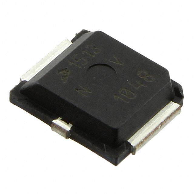
| 产品图片 |
|
| 产品型号 | JCA1048S05 |
| rohs | 无铅 / 符合限制有害物质指令(RoHS)规范要求 |
| 产品系列 | JCA |
| 其它名称 | 1470-1792-5 |
| 功率(W)-制造系列 | 10W |
| 功率(W)-最大值 | 8W |
| 包装 | 管件 |
| 大小/尺寸 | 1.00" 长 x 0.80" 宽 x 0.39" 高 (25.4mm x 20.3mm x 10.0mm) |
| 安装类型 | 通孔 |
| 封装/外壳 | 24-DIP 模块(7 引线) |
| 工作温度 | -40°C ~ 100°C |
| 效率 | 89% |
| 标准包装 | 16 |
| 特性 | OCP,OVP,SCP,UVLO |
| 特色产品 | http://www.digikey.cn/product-highlights/zh/jca10-series-10-w-ultracompact-dcdc-converters/51055http://www.digikey.cn/product-highlights/zh/jca-series/52670 |
| 电压-输入(最大值) | 75V |
| 电压-输入(最小值) | 36V |
| 电压-输出1 | 5V |
| 电压-输出2 | - |
| 电压-输出3 | - |
| 电压-隔离 | 1.5kV(1500V) |
| 电流-输出(最大值) | 1.6A |
| 类型 | 隔离模块 |
| 输出数 | 1 |


PDF Datasheet 数据手册内容提取
10 Watts C xppower.com D JCA Series - C D • Compact 1.0” x 0.8” Metal Package • Industry Standard Pin Out • 2:1 Input Range • Single & Dual Outputs • Operating Temperature -40 °C to +100 °C • UL, CB, & TUV Approval • 3 Year Warranty Specification Input General Input Voltage Range • 5 V (4.5-9.0 VDC) Efficiency • See table 12 V (9-18 VDC) Isolation • 1500 VDC Input to Output, basic insulation 24 V (18-36 VDC) 500 VDC Input to Case 48 V (36-75 VDC) 500 VDC Output to Case Input Current • See table Switching Frequency • 300 kHz typical Input Filter • Pi network Power Density • 31.25 W/in3 Input Reflected • 80 mA, 5 V input models, 30 mA all others MTBF • >950 kHrs to MIL-HDBK-217F at 25 °C, Ripple Current 12 µH inductor, 5 Hz to 20 MHz GB Input Surge • 5 V models 10 V for 1 s max, 12 V models 25 V for 1 s max, Environmental 24 V models 50 V for 1 s max, 48 V models 100 V for 1 s max Operating Temperature • -40 °C to +100 °C output power derates from 100% load at +70 °C linearly to Output 0% load at +100 °C Case Temperature • +100 °C max Output Voltage • See table Storage Temperature • -55 °C to +125 °C Initial Set Accuracy • ±1% max Cooling • Convection cooled Start Up Delay • 30 ms max Operating Humidity • Up to 95% RH, non-condensing Start Up Rise Time • 3.5 ms typical Minimum Load • No minimum load required EMC & Safety Line Regulation • ±0.3% Emissions • EN55022, level A conducted Load Regulation • ±1% (level B with external components, see Cross Regulation • ±5% on dual output models with one application note), level B radiated output at 5% load and other varied from ESD Immunity • EN61000-4-2, level 2 Perf Criteria A 5% to 100% Radiated Immunity • EN61000-4-3, 3 V/m Perf Criteria A Transient Response • 4% max deviation, recovery to within Conducted Immunity • EN61000-4-6, 3 V rms Perf Criteria A 1% in <500 µs for a 25% load change at 1 A/µs Magnetic Fields • EN61000-4-8, 10 A/m, Perf Criteria A Ripple & Noise • 50 mV pk-pk, 20 MHz bandwidth Safety Approvals • IEC60950-1, EN60950-1, UL60950-1, CSA C22.2 No. 60950-1-03, CE Mark LVD Overcurrent Protection • 150% typical, trip and restart (hiccup mode) Short Circuit Protection • Continuous with auto recovery Overvoltage Protection • 150% typical, Recycle input to reset Temperature • ±0.05%/°C Coefficient
JCA10 D Models and Ratings C Input Current(2) Max. Input Voltage(1) Output Voltage Output Current No Load Full Load Efficiency Capacitive Load Model Number - 3.3 VDC 2.42 A 100 mA 1.905 A 82% 3300 µF JCA1005S03 D 5.0 VDC 1.60 A 84 mA 1.839 A 86% 2200 µF JCA1005S05 12.0 VDC 0.83 A 126 mA 2.324 A 85% 1000 µF JCA1005S12 C 4.5-9.0 VDC 15.0 VDC 0.66 A 120 mA 2.271 A 86% 940 µF JCA1005S15 ±5.0 VDC ±0.80 A 129 mA 1.918 A 82% 1000 µF JCA1005D01 ±12.0 VDC ±0.42 A 126 mA 2.388 A 84% 470 µF JCA1005D02 ±15.0 VDC ±0.33 A 105 mA 2.297 A 85% 470 µF JCA1005D03 3.3 VDC 2.42 A 52 mA 0.784 A 84% 3300 µF JCA1012S03 5.0 VDC 1.60 A 49 mA 0.745 A 89% 2200 µF JCA1012S05 12.0 VDC 0.83 A 42 mA 0.930 A 89% 1000 µF JCA1012S12 9-18 VDC 15.0 VDC 0.66 A 42 mA 0.916 A 89% 940 µF JCA1012S15 ±5.0 VDC ±0.80 A 45 mA 0.778 A 85% 1000 µF JCA1012D01 ±12.0 VDC ±0.42 A 44 mA 0.944 A 88% 470 µF JCA1012D02 ±15.0 VDC ±0.33 A 44 mA 0.915 A 89% 470 µF JCA1012D03 3.3 VDC 2.42 A 28 mA 0.388 A 85% 3300 µF JCA1024S03 5.0 VDC 1.60 A 27 mA 0.375 A 88% 2200 µF JCA1024S05 12.0 VDC 0.83 A 19 mA 0.461 A 89% 1000 µF JCA1024S12 18-36 VDC 15.0 VDC 0.66 A 18 mA 0.455 A 90% 940 µF JCA1024S15 ±5.0 VDC ±0.80 A 16 mA 0.387 A 85% 1000 µF JCA1024D01 ±12.0 VDC ±0.42 A 22 mA 0.469 A 89% 470 µF JCA1024D02 ±15.0 VDC ±0.33 A 25 mA 0.455 A 90% 470 µF JCA1024D03 3.3 VDC 2.42 A 13 mA 0.199 A 82% 3300 µF JCA1048S03 5.0 VDC 1.60 A 11 mA 0.186 A 89% 2200 µF JCA1048S05 12.0 VDC 0.83 A 7 mA 0.231 A 89% 1000 µF JCA1048S12 36-75 VDC 15.0 VDC 0.66 A 9 mA 0.229 A 89% 940 µF JCA1048S15 ±5.0 VDC ±0.80 A 5 mA 0.194 A 85% 1000 µF JCA1048D01 ±12.0 VDC ±0.42 A 9 mA 0.236 A 89% 470 µF JCA1048D02 ±15.0 VDC ±0.33 A 10 mA 0.229 A 89% 470 µF JCA1048D03 Notes 1. Nominal input voltage 5, 12, 24 or 48 VDC. 3. Efficiency is measured at nominal input and full load at 25 °C. 2. Input current is at nominal input voltage. Mechanical Details 0.02 (0.5) 0.1 (2.5) 23 2 22 3 0(0.0.52) (01.56.02)(02.29.09) (12.50.40) BOVTIETWOM P2in SingPl-eINV Oi nCuOtpNuNtECTIONS Dual- VOinutput 3 -Vin -Vin 9 No pin Common 16 9 11 N/C -Vout 0.20 14 +Vout +Vout (5.1) 16 -Vout Common 14 11 22 +Vin +Vin 23 +Vin +Vin 0.09 (±0.02) 0.60 (15.2) 1. All dimensions in inches (mm) (2.4 ±0.5) 2. Weight: 0.03 lbs (12 g) 0.4 ±0.02 0.15 0.80 ±0.02 3. Pin diameter tolerance: ±0.00079 (±0.02) (10.0 ± 0.5) (3.8) 4. Pin pitch tolerance: ±0.01 (±0.25) (20.3 ±0.5) 5. Case tolerance: ±0.02 (±0.5) Application Note Input Filter To meet level B conducted emissions. 1 L1 2 +Vin 4.7µF/100V C1 JCA10 4 3 -Vin 470µH Common mode choke 14 April 16