ICGOO在线商城 > 集成电路(IC) > 嵌入式 - CPLD(复杂可编程逻辑器件) > ISPLSI 2032A-80LTN44
 Datasheet下载
- 型号: ISPLSI 2032A-80LTN44
- 制造商: Lattice
- 库位|库存: xxxx|xxxx
- 要求:
| 数量阶梯 | 香港交货 | 国内含税 |
| +xxxx | $xxxx | ¥xxxx |
查看当月历史价格
查看今年历史价格
ISPLSI 2032A-80LTN44产品简介:
ICGOO电子元器件商城为您提供ISPLSI 2032A-80LTN44由Lattice设计生产,在icgoo商城现货销售,并且可以通过原厂、代理商等渠道进行代购。 ISPLSI 2032A-80LTN44价格参考。LatticeISPLSI 2032A-80LTN44封装/规格:嵌入式 - CPLD(复杂可编程逻辑器件), 。您可以下载ISPLSI 2032A-80LTN44参考资料、Datasheet数据手册功能说明书,资料中有ISPLSI 2032A-80LTN44 详细功能的应用电路图电压和使用方法及教程。
Lattice Semiconductor Corporation(莱迪思半导体公司)生产的ISPLSI 2032A-80LTN44是一款嵌入式CPLD(复杂可编程逻辑器件),广泛应用于需要灵活逻辑设计和小型化解决方案的场景。以下是其主要应用场景:

 1. 工业自动化
   - 在工业控制中,ISPLSI 2032A可用于实现复杂的时序逻辑、信号处理和接口转换。例如,用于PLC(可编程逻辑控制器)中的输入输出信号管理和协议转换。
   - 提供高可靠性和低功耗特性,适合在恶劣环境下运行。

 2. 通信设备
   - 适用于小型通信模块或网络设备中,用于信号同步、数据缓冲和接口扩展。
   - 可用作桥接芯片,连接不同标准的通信接口(如UART、SPI、I2C等)。

 3. 消费电子
   - 在消费电子产品中,该器件可用于实现按键扫描、LED驱动、电源管理等功能。
   - 提供定制化的逻辑功能,帮助降低系统复杂度和成本。

 4. 汽车电子
   - 用于车载信息娱乐系统、传感器接口和控制单元中,提供灵活的逻辑配置。
   - 支持信号调理和多路复用,满足汽车电子对可靠性和实时性的要求。

 5. 医疗设备
   - 在便携式医疗设备中,用于信号采集、处理和传输。例如,心率监测仪或血糖仪中的逻辑控制。
   - 其低功耗特性有助于延长电池寿命。

 6. 航空航天与国防
   - 在高可靠性需求的应用中,CPLD可用于实现关键逻辑功能,如信号路由、状态机控制和故障检测。
   - 提供抗辐射选项(部分系列),适用于极端环境。

 7. 嵌入式系统开发
   - 作为原型开发工具,快速实现特定逻辑功能,加速产品上市时间。
   - 通过编程灵活性支持多种应用场景,减少硬件设计变更。

 总结
ISPLSI 2032A-80LTN44凭借其高性能、低功耗和小型封装特点,适合需要高效逻辑控制和接口扩展的应用场景。其典型应用包括工业控制、通信设备、消费电子、汽车电子、医疗设备以及航空航天等领域,能够显著提升系统的灵活性和可靠性。
| 参数 | 数值 |
| 产品目录 | 集成电路 (IC) |
| 描述 | IC CPLD 32MC 15NS 44TQFP |
| 产品分类 | |
| I/O数 | 32 |
| 品牌 | Lattice Semiconductor Corporation |
| 数据手册 | |
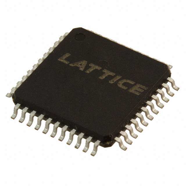
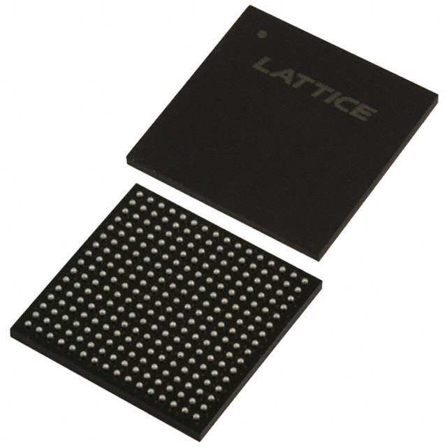
| 产品图片 |
|
| 产品型号 | ISPLSI 2032A-80LTN44 |
| rohs | 无铅 / 符合限制有害物质指令(RoHS)规范要求 |
| 产品系列 | ispLSI® 2000A |
| 供应商器件封装 | 44-TQFP(10x10) |
| 其它名称 | 220-1605 |
| 包装 | 托盘 |
| 可编程类型 | 系统内可编程 |
| 安装类型 | 表面贴装 |
| 宏单元数 | 32 |
| 封装/外壳 | 44-TQFP |
| 工作温度 | 0°C ~ 70°C |
| 延迟时间tpd(1)最大值 | 15.0ns |
| 栅极数 | 1000 |
| 标准包装 | 160 |
| 电源电压-内部 | 4.75 V ~ 5.25 V |
| 逻辑元件/块数 | 8 |


- 商务部:美国ITC正式对集成电路等产品启动337调查
- 曝三星4nm工艺存在良率问题 高通将骁龙8 Gen1或转产台积电
- 太阳诱电将投资9.5亿元在常州建新厂生产MLCC 预计2023年完工
- 英特尔发布欧洲新工厂建设计划 深化IDM 2.0 战略
- 台积电先进制程称霸业界 有大客户加持明年业绩稳了
- 达到5530亿美元!SIA预计今年全球半导体销售额将创下新高
- 英特尔拟将自动驾驶子公司Mobileye上市 估值或超500亿美元
- 三星加码芯片和SET,合并消费电子和移动部门,撤换高东真等 CEO
- 三星电子宣布重大人事变动 还合并消费电子和移动部门
- 海关总署:前11个月进口集成电路产品价值2.52万亿元 增长14.8%

PDF Datasheet 数据手册内容提取
Lead- Free Package ispLSI® 2032/A Options Available! In-System Programmable High Density PLD Features Functional Block Diagram • ENHANCEMENTS — ispLSI 2032A is Fully Form and Function Compatible to the ispLSI 2032, with Identical Timing S Specifcations and Packaging N — ispLSI 2032A is Built on an Advanced 0.35 Micron E2CMOS® Technology G S e • HIGH DENSITY PROGRAMMABLE LOGIC A0 Global Routing Pool I A7 e — 1000 PLD Gates RP) (GRP) S RP) O — 32 I/O Pins, Two Dedicated Inputs O O — 32 Registers us Pool ( A1 DQ E A6 Pool ( us rd S ——— HWMSmiaigdcahehl lSiI nnLpepoesuge,ti dc AG GdBadlltooirnbecgsak sl f S oIDnirzte eeFc rafocosdorte n CRrnsoae,nu cednttotcem.rs L, oSgtaicte Input B Output Routing A2 GLB WLAor rgaicy DDDDQQQ A5 Output Routing Input B ering elect d A3 A4 I • HIGH PERFORMANCE E2CMOS® TECHNOLOGY E n e — fmax = 180 MHz Maximum Operating Frequency fo v N i — tpd = 5.0 ns Propagation Delay r c m e — TTL Compatible Inputs and Outputs s — Electrically Erasable and Reprogrammable R 0139Bisp/2000 a t h — Non-Volatile i O o a — 100% Tested at Time of Manufacture n v — Unused Product Term Shutdown Saves Power F Description e s • IN-SYSTEM PROGRAMMABLE e b E The ispLSI 2032 and 2032A are High Density Program- c e — In-System Programmable (ISP™) 5V Only t e — Increased Manufacturing Yields, Reduced Ti2me-to- mable Logic Devices. The devices contain 32 Registers, io n Market and Improved Product Quality 3 32 Universal I/O pins, two Dedicated Input Pins, three n d • —OFFREeRpSro TgHraEm E SAoSlEde OreFd U DSeEv iAcNesD f FoAr FSaTs St0eYrS PTrEoMtotyping Dinepduitc paitne da nCdlo ac kG Ilnopbuatl RPoinust,i nogn e P doeodl i(cGaRtePd) .G Tlohbea Gl OREP fo is c SPEED OF PLDs WITH THE DENSITY 2AND FLEXIBILITY provides complete interconnectivity between all of these r o p OF FIELD PROGRAMMABLE GATE ARRAYS elements. The ispLSI 2032 and 2032A feature 5V in- n — Complete Programmable DeSvIice Can Combine Glue system programmability and in-system diagnostic ro ti Logic and Structured Designs capabilities. The ispLSI 2032 and 2032A offer non- d n L u u — Enhanced Pin Locking Capability volatile reprogrammability of the logic, as well as the c e — Three Dedicated Clopck Input Pins interconnect to provide truly reconfigurable systems. t d — Synchronous ansd Asynchronous Clocks The basic unit of logic on these devices is the Generic s . — Programmable Output Slew Rate Control to t Minimize Swiitching Noise Logic Block (GLB). The GLBs are labeled A0, A1 .. A7 a t — Flexible PEin Placement (Figure 1). There are a total of eight GLBs in the ispLSI u — Optimized Global Routing Pool Provides Global 2032 and 2032A devices. Each GLB is made up of four s S . Interconnectivity macrocells. Each GLB has 18 inputs, a programmable — LeUad-Free Package Options AND/OR/Exclusive OR array, and four outputs which can be configured to be either combinatorial or registered. Inputs to the GLB come from the GRP and dedicated inputs. All of the GLB outputs are brought back into the GRP so that they can be connected to the inputs of any GLB on the device. Copyright © 2006 Lattice Semiconductor Corp. All brand or product names are trademarks or registered trademarks of their respective holders. The specifications and information herein are subject to change without notice. LATTICE SEMICONDUCTOR CORP., 5555 Northeast Moore Ct., Hillsboro, Oregon 97124, U.S.A. August 2006 Tel. (503) 268-8000; 1-800-LATTICE; FAX (503) 268-8556; http://www.latticesemi.com 2032_11 1
Specifications ispLSI 2032/A Functional Block Diagram Figure 1. ispLSI 2032/A Functional Block Diagram GOE 0 S N G S e I S e O E I/O 0 I/O 31 r I/O 1 A0 A7 I/O 30 d S I/O 2 D I/O 29 e e II//OO 34 ORP) W ORP) II//OO 2287 rin lec II//IIIIOOI/////OOOOO 11 6789015 Input Bus put Routing Pool ( AA12 Global (RGoRuPtin)g Pool N E AA65 put Routing Pool ( Input Bus IIIIIII///////OOOOOOO 22222226543210 g Inform t device I/O 12 Out R Out I/O 19 a s III///OOO 111345 A3 O A4 III///OOO 111876 tio ha SDI/IN 0 F n v SDO/IN 1 s e E K 0K 1K 2 ec be MODE 2 CLCLCL t e ispEN io n 3 n d N o*Yte1s :a nd RESET are multiplexed on2 the s0ame pin Y1S*C/RLEKS/YYE02T fo isc r 0139B(1)isp/2000 p o I n S ro t i The devices also have 32L I/O cells, each of which is All of these signals are made available to the inputs of the d n u u directly connected to anp I/O pin. Each I/O cell can be GLBs. Delays through the GRP have been equalized to c e individually programmed to be a combinatorial input, minimize timing skew. t d output or bi-directiosnal I/O pin with 3-state control. The s . signal levels are TiTL compatible voltages and the output Clocks in the ispLSI 2032 and 2032A devices are se- ta drivers can soEurce 4 mA or sink 8 mA. Each output can lected using the dedicated clock pins. Three dedicated t u clock pins (Y0, Y1, Y2) or an asynchronous clock can be be programmed independently for fast or slow output s S slew rate to minimize overall output switching noise. selected on a GLB basis. The asynchronous or Product . U Term clock can be generated in any GLB for its own clock. Eight GLBs, 32 I/O cells, two dedicated inputs and two ORPs are connected together to make a Megablock (Figure 1). The outputs of the eight GLBs are connected to a set of 32 universal I/O cells by the ORP. Each ispLSI 2032 and 2032A device contains one Megablock. The GRP has as its inputs, the outputs from all of the GLBs and all of the inputs from the bi-directional I/O cells. 2
Specifications ispLSI 2032/A Absolute Maximum Ratings 1 Supply Voltage V ...................................-0.5 to +7.0V cc Input Voltage Applied........................-2.5 to V +1.0V CC Off-State Output Voltage Applied.....-2.5 to V +1.0V CC S Storage Temperature................................-65 to 150°C N Case Temp. with Power Applied ..............-55 to 125°C G S e Max. Junction Temp. (TJ) with Power Applied ... 150°C SI e O 1. Stresses above those listed under the “Absolute Maximum Ratings” may cause permanent damaEge to the device. Functional operation of the device at these or at any other conditions above those indicated in the operational sections of this specification rd S is not implied (while programming, follow the programming specifications). D e e ri le W n c DC Recommended Operating Condition g t d E I n e SYMBOL PARAMETER N MIN. MAX. UNITS fo v i r c VCC Supply Voltage Commercial TAR = 0°C to + 70°C 4.75 5.25 V m es Industrial TA = -40°C to + 85°C 4.5 5.5 V a VIL Input Low Voltage O 0 0.8 V ti h o a VIH Input High Voltage F 2.0 Vcc+1 V n v e Table 2 - 0005/2032 s E e b c e 2 t e Capacitance (TA=25°C, f=1.0 MHz)3 ion n d SYMBOL PARAME0TER TYPICAL UNITS TEST CONDITIONS fo is 2 c C1 Dedicated Input Cap acitance 6 pf VC C = 5.0V, VI N = 2.0V r p o C2 I/O CapacitanceSI 7 pf VC C = 5.0V, VI /O = 2.0V ro nt i C3 Clock CapacLitance 10 pf VC C = 5.0V, VY = 2.0V d n Table 2-0006/2032 u u p c e t d s s . Data Retentioin Specifications t a E t u PARAMETER MINIMUM MAXIMUM UNITS s S . Data Retention 20 – Years U Erase/Reprogram Cycles 10000 – Cycles Table 2-0008A-isp 3
Specifications ispLSI 2032/A Switching Test Conditions Figure 2. Test Load Input Pulse Levels GND to 3.0V Input Rise and Fall Time -135, -150, -180 ≤ 1.5 ns + 5V 10% to 90% -80, -110 ≤ 3 ns R1 Input Timing Reference Levels 1.5V S Output Timing Reference Levels 1.5V Device Test Output NPoint Output Load See Figure 2 3-state levels are measured 0.5V from Table 2-0003/2032 R2 CL* G S steady-state active level. e I S e Output Load Conditions (see Figure 2) O * E CL includes Test Fixture and Probe Capacitance. r d S TEST CONDITION R1 R2 CL D 0213A e e A 470Ω 390Ω 35pF ri le W n c Active High ∞ 390Ω 35pF B g t Active Low 470Ω 390Ω 35pF d E I n e Active High to Z C at VO H -0.5V ∞ 390Ω 5pF N fo vi Active Low to Z r c at VO L +0.5V 470Ω 390Ω 5pF R m es Table 2 - 0004A a O t h i o a F n v DC Electrical Characteristics e s Over RecommeEnded Operating Conditions e b c e SYMBOL PARAMETER 2 CONDITION MIN. TYP.3 MAX. UNITS tio en VOL Output Low Voltage 3IO L = 8 mA – – 0.4 V n d VOH Output High Voltage 0 IO H = -4 mA 2.4 – – V fo is IIL Input or I/O Low Leakage Cur2rent 0V ≤ VI N ≤ VI L (Max.) – – -10 μA r p co IIIIHL-isp IisnppEuNt o Irn Ip/Out HLiogwh LLeeaakkSaaggIee CCuurrrreenntt 30.V5 V≤ V≤I NV ≤I N V≤ ILV CC –– –– -11500 μμAA rod ntin L IIL-PU I/O Active Pull-Up Current 0V ≤ VI N ≤ VIL – – -150 μA u u IOS1 Output Short Cpircuit Current VC C = 5V, VO U T = 0.5V – – -200 mA ct ed ICC2, 4 Operaitings Power Supply Current VI L = 0.0V, VI H = 3.0V Comm. O-1t8h0e,r s-150 –– 4600 –– mmAA sta . f = 1 MHz E TOGGLE t Industrial – 40 – mA u s S Table 2-0007/2032 1. One output at a time for a maximum duration of one second. V = 0.5V was selected to avoid test problems . OUT by teUster ground degradation. Characterized but not 100% tested. 2. Measured using two 16-bit counters. 3. Typical values are at VC C = 5V and TA = 25°C. 4. Maximum I varies widely with specific device configuration and operating frequency. Refer to the Power Consumption CC section of this data sheet and Thermal Management section of the Lattice Semiconductor Data Book or CD-ROM to estimate maximum I . CC 4
Specifications ispLSI 2032/A External Timing Parameters Over Recommended Operating Conditions TEST4 -180 -150 -135 PARAMETER #2 DESCRIPTION1 UNITS COND. MIN. MAX. MIN. MAX. MIN. MAX. tpd1 A 1 Data Prop. Delay, 4PT Bypass, ORP Bypass – 5.0 – 5.5 – 7.5 ns S tpd2 A 2 Data Prop. Delay – 7.5 – 8.0 – 10.0 ns N fmax A 3 Clk Frequency with Internal Feedback3 180 – 154 – 137 – MHz fmax (Ext.) – 4 Clk Frequency with Ext. Feedback ( 1 ) 125 – 111 – 100G – MHz S tsu2 + tco1 fmax (Tog.) – 5 Clk Frequency, Max. Toggle 200 – 167 – I167 – MHz e S e tsu1 – 6 GLB Reg Setup Time before Clk, 4 PT Bypass 3.0 – 3.0 – 4.0 – ns O E tco1 A 7 GLB Reg. Clk to Output Delay, ORP Bypass – 4.0 – 4.5 – 4.5 ns r d S th1 – 8 GLB Reg. Hold Time after Clk, 4 PT Bypass 0.0 – 0D.0 – 0.0 – ns e e tsu2 – 9 GLB Reg. Setup Time before Clk 4.0 – 4.5 – 5.5 – ns ri le W n c tco2 – 10 GLB Reg. Clk to Output Delay – 4.5 – 5.0 – 5.5 ns g t th2 – 11 GLB Reg. Hold Time after Clk 0.E0 – 0.0 – 0.0 – ns I d n e tr1 A 12 Ext. Reset Pin to Output Delay N – 7.0 – 8.0 – 10.0 ns fo v i trw1 – 13 Ext. Reset Pulse Duration 4.0 – 4.5 – 5.0 – ns r c m e tptoeen B 14 Input to Output Enable R – 10.0 – 11.0 – 12.0 ns s a tptoedis C 15 Input to Output Disable O – 10.0 – 11.0 – 12.0 ns t h i o a tgoeen B 16 Global OE Output Enable – 5.0 – 5.0 – 6.0 ns F n v tgoedis C 17 Global OE Output Disable – 5.0 – 5.0 – 6.0 ns e s twh – 18 Ext. Synchronous Clk PulEse Duration, High 2.5 – 3.0 – 3.0 – ns e b c e twl – 19 Ext. Synchronous Clk2 Pulse Duration, Low 2.5 – 3.0 – 3.0 – ns t e io n 1. Unless noted otherwise, all parameters use th3e GRP, 20 PTXOR path, ORP and Y0 clock. Table 2-0030B-180/2032 n d 23.. RSteafnedr atord T 1im6-inbgit Mcooudnetel irn u tshiinsg d GatRaP s hfeeeedt bfoa0rc fku.rther details. fo is 2 c 4. Reference Switching Test Conditions section. r p o I n S ro t i d n L u u p c e t d s s . i t a E t u s S . U 5
Specifications ispLSI 2032/A External Timing Parameters Over Recommended Operating Conditions TEST4 -110 -80 PARAMETER #2 DESCRIPTION1 UNITS COND. MIN. MAX. MIN. MAX. tpd1 A 1 Data Propagation Delay, 4PT Bypass, ORP Bypass – 10.0 – 15.0 ns S tpd2 A 2 Data Propagation Delay – 13.0 – 18.5 ns N fmax A 3 Clock Frequency with Internal Feedback3 111 – 84.0 – MHz fmax (Ext.) – 4 Clock Frequency with External Feedback( t s u 2 1 + t c o 1) 77.0 – 57.0G – MHz S fmax (Tog.) – 5 Clock Frequency, Max. Toggle 125 – I83.0 – MHz e S e tsu1 – 6 GLB Reg. Setup Time before Clock, 4 PT Bypass 5.5 – 7.5 – ns O tco1 A 7 GLB Reg. Clock to Output Delay, ORP Bypass – E5.5 – 8.0 ns r d S th1 – 8 GLB Reg. Hold Time after Clock, 4 PT Bypass 0.D0 – 0.0 – ns e e tsu2 – 9 GLB Reg. Setup Time before Clock 7.5 – 9.5 – ns ri le W n c tco2 – 10 GLB Reg. Clock to Output Delay – 6.5 – 9.5 ns g t th2 – 11 GLB Reg. Hold Time after Clock E 0.0 – 0.0 – ns I d n e tr1 A 12 Ext. Reset Pin to Output Delay N – 13.5 – 19.5 ns fo v trw1 – 13 Ext. Reset Pulse Duration 6.5 – 10.0 – ns r ic m e tptoeen B 14 Input to Output Enable R – 14.5 – 24.0 ns s a tptoedis C 15 Input to Output Disable O – 14.5 – 24.0 ns t h i tgoeen B 16 Global OE Output Enable – 7.0 – 12.0 ns o a F n v tgoedis C 17 Global OE Output Disable – 7.0 – 12.0 ns e s twh – 18 External Synchronous CloEck Pulse Duration, High 4.0 – 6.0 – ns e b c e twl – 19 External Synchronou2s Clock Pulse Duration, Low 4.0 – 6.0 – ns t e 1. Unless noted otherwise, all parameters use the3 GRP, 20 PTXOR path, ORP and Y0 clock. Table 2-0030B-110/2032 ion n d 2. Refer to Timing Model in this data sheet for further details. 3. Standard 16-bit counter using GRP feedba0ck. fo is 4. Reference Switching Test Conditions se2ction. r c p o I n S ro t i d n L u u p c e t d s s . i t a E t u s S . U 6
Specifications ispLSI 2032/A Internal Timing Parameters1 Over Recommended Operating Conditions -180 -150 -135 PARAMETER #2 DESCRIPTION UNITS MIN. MAX. MIN. MAX. MIN. MAX. Inputs S tio 20 Input Buffer Delay – 0.6 – 0.6 – 1.1 ns N tdin 21 Dedicated Input Delay – 1.1 – 1.3 – 2.4 ns G GRP S tgrp 22 GRP Delay – 0.7 – 0.7 I– 1.3 ns e S e GLB O t4ptbpc 23 4 Product Term Bypass Path Delay (Combinatorial) – 2.3 – E2.6 – 3.6 ns r d S t4ptbpr 24 4 Product Term Bypass Path Delay (Registered) – 3.1 D– 3.1 – 3.6 ns e e t1ptxor 25 1 Product Term/XOR Path Delay – 3.6 – 4.3 – 5.0 ns ri le W n c t20ptxor 26 20 Product Term/XOR Path Delay – 4.1 – 4.6 – 5.1 ns g t txoradj 27 XOR Adjacent Path Delay3 –E 4.8 – 5.0 – 5.6 ns I d n e tgbp 28 GLB Register Bypass Delay N – 0.2 – 0.0 – 0.0 ns fo v i tgsu 29 GLB Register Setup Time before Clock 0.5 – 0.7 – 0.3 – ns r c m e tgh 30 GLB Register Hold Time after Clock R 1.8 – 1.8 – 3.0 – ns s a tgco 31 GLB Register Clock to Output Delay O – 0.7 – 0.8 – 0.7 ns t h i o a tgro 32 GLB Register Reset to Output Delay – 1.0 – 1.2 – 1.1 ns F n v tptre 33 GLB Product Term Reset to Register Delay – 2.8 – 2.9 – 4.4 ns e s tptoe 34 GLB Product Term Output Enable Eto I/O Cell Delay – 5.9 – 6.9 – 6.4 ns e b c e tptck 35 GLB Product Term Clock Dela2y 2.5 3.8 2.5 4.1 2.9 5.2 ns t e io n ORP 3 n d ttoorrppbp 3367 OORRPP DByeplaayss Delay20 –– 00..72 –– 00..83 –– 10..33 nnss fo isc r Outputs p o I n tob 38 Output BuffeSr Delay – 1.2 – 1.3 – 1.2 ns ro t i tsl 39 Output SLlew Limited Delay Adder – 10.0 – 10.0 – 10.0 ns d n u u toen 40 I/O Cpell OE to Output Enabled – 2.8 – 2.8 – 3.2 ns c e t d todis 41 sI/O Cell OE to Output Disabled – 2.8 – 2.8 – 3.2 ns s . tgoe 4i2 Global Output Enable – 2.2 – 2.2 – 2.8 ns t a Clocks E t u tgy0 S 43 Clock Delay, Y0 to Global GLB Clock Line (Ref. clock) 1.9 1.9 2.1 2.1 2.3 2.3 ns s . tgy1/U2 44 Clock Delay, Y1 or Y2 to Global GLB Clock Line 1.9 1.9 2.1 2.1 2.3 2.3 ns Global Reset tgr 45 Global Reset to GLB – 4.1 – 4.7 – 6.4 ns 1. Internal Timing Parameters are not tested and are for reference only. Table 2-0036C-180/2032 2. Refer to Timing Model in this data sheet for further details. 3. The XOR adjacent path can only be used by hard macros. 7
Specifications ispLSI 2032/A Internal Timing Parameters1 Over Recommended Operating Conditions -110 -80 PARAMETER #2 DESCRIPTION UNITS MIN. MAX. MIN. MAX. Inputs S tio 20 Input Buffer Delay – 1.7 – 2.2 ns N tdin 21 Dedicated Input Delay – 3.4 – 4.8 ns G GRP S tgrp 22 GRP Delay – 1.7 I– 2.6 ns e S e GLB O E t4ptbpc 23 4 Product Term Bypass Path Delay (Combinatorial) – 4.9 – 7.2 ns r d S t4ptbpr 24 4 Product Term Bypass Path Delay (Registered) –D 4.8 – 7.2 ns e e t1ptxor 25 1 Product Term/XOR Path Delay – 6.2 – 8.8 ns ri le W n c t20ptxor 26 20 Product Term/XOR Path Delay – 6.8 – 9.2 ns g t d txoradj 27 XOR Adjacent Path Delay3 E – 7.5 – 10.2 ns I n e tgbp 28 GLB Register Bypass Delay N – 0.1 – 0.0 ns fo v i tgsu 29 GLB Register Setup Time befor Clock 0.5 – 0.1 – ns r c m e tgh 30 GLB Register Hold Time after Clock R 4.0 – 6.0 – ns s a tgco 31 GLB Register Clock to Output Delay O – 0.6 – 0.4 ns ti h o a tgro 32 GLB Register Reset to Output Delay F – 1.8 – 2.2 ns n v tptre 33 GLB Product Term Reset to Register Delay – 5.9 – 8.8 ns s e tptoe 34 GLB Product Term Output Enable Eto I/O Cell Delay – 7.1 – 12.8 ns e b c e tptck 35 GLB Product Term Clock Dela2y 4.0 7.0 5.5 9.5 ns t e io n ORP 3 n d torp 36 ORP Delay 0 – 1.5 – 2.1 ns fo is torpbp 37 ORP Bypass Delay2 – 0.5 – 0.6 ns r c Outputs p o I n tob 38 Output BuffeSr Delay – 1.2 – 2.4 ns ro ti d n tsl 39 Output SLlew Limited Delay Adder – 10.0 – 10.0 ns u u toen 40 I/O Cpell OE to Output Enabled – 4.0 – 6.4 ns c e t d todis 41 Is/O Cell OE to Output Disabled – 4.0 – 6.4 ns s . tgoe 4i2 Global Output Enable – 3.0 – 5.6 ns ta Clocks E tu tgy0 S 43 Clock Delay, Y0 to Global GLB Clock Line (Ref. clock) 3.2 3.2 4.6 4.6 ns s . tgy1/2U 44 Clock Delay, Y1 or Y2 to Global GLB Clock Line 3.2 3.2 4.6 4.6 ns Global Reset tgr 45 Global Reset to GLB – 9.0 – 12.8 ns 1. Internal Timing Parameters are not tested and are for reference only. Table 2-0036C-110/2032 2. Refer to Timing Model in this data sheet for further details. 3. The XOR adjacent path can only be used by hard macros. 8
Specifications ispLSI 2032/A ispLSI 2032/A Timing Model I/O Cell GRP GLB ORP I/O Cell Feedback S Ded. In Comb 4 PT Bypass #23 #21 N I/O Delay GRP Reg 4 PT Bypass GLB Reg Bypass ORP Bypass #38, I/O Pin I/O Pin #20 #22 #24 #28 #37 G39 (Input) (Output) S 20 PT GLB Reg ORP XOR Delays Delay Delay I e D Q S e #25, 26, 27 #36 RST E O #45 #29, 30, r Reset 31, 32 d S D e e ri le Control RE W n c PTs OE g t #333,5 34, CK E #40, 41 In de Y0,1,2 #43, 44 N fo vi r c GOE 0 #42 m e R 0491/2000 s a O t h i o a Derivations of tsu, th and tco from the Product TeFrm Clock1 n v e tsu = Logic + Reg su - Clock (min) E se b = (tio + tgrp + t20ptxor) + (tgsu) - (tio + tgrp + tptck(min)) c e = (#20+ #22+ #26) + (#29) - (#202+ #22+ #35) t e io n 2.1 ns = (0.6 + 0.7 + 4.1) + (0.5) - (03.6 + 0.7 + 2.5) n d th == C(tiloo c+k t(gmrpa x+) t+p Rtcekg(m h2a -x )L)0o +g i(ctgh) - (tio + tgrp + t20ptxor) fo isc r = (#20+ #22+ #35) + (#30) - (#20+ #22+ #26) p o 1.5 ns = (0.6 + 0.7 + 3.8I) + (1.8) - (0.6 + 0.7 + 4.1) n S ro t tco = Clock (max) + Reg co + Output d in = (tio + tgrLp + tptck(max)) + (tgco) + (torp + tob) u u = (#20+p #22+ #35) + (#31) + (#36 + #38) c e 7.7 ns = (0.6 + 0.7 + 3.8) + (0.7) + (0.7 + 1.2) t d s s . i t a Note: Calculati ons are based upon timing specifications for the ispLSI 2032/A-180L E t u Table 2- 0042-16/2032 s S . U 9
Specifications ispLSI 2032/A Power Consumption Power consumption in the ispLSI 2032 and 2032A de- used. Figure 4 shows the relationship between power vices depends on two primary factors: the speed at which and operating speed. the device is operating and the number of Product Terms Figure 4. Typical Device Power Consumption vs fmax S N G S e I S e 120 O E 110 r d S D ispLSI 2032/A (-150, -180) e e ) 100 ri le mA 90 W n c g t C ( d 80 E I C n e I 70 N fo v i ispLSI 2032/A (-80, -110, -135) r c 60 m e R s a 50 O t h i o a 40 F n v e s E e b 1 20 40 60 80 100 120 140 160 180 c e 2 fmax (MHz) tio en 3Notes: Configuration of Two 16-bit Counters n d 0 Typical Current at 5V, 25° C fo is 2 c r ICC can be estimated for the ispLSI 2032/A using the following equation: p o I n For 2032/A -150, -180: ICC(mA)S = 30 + (# of PTs * 0.46) + (# of nets * Max freq * 0.012) ro ti d n For 2032/A -135, -110, -80: LICC(mA) = 21 + (# of PTs * 0.30) + (# of nets * Max freq * 0.012) u u p c e Where: t d # of PTs = Numbesr of Product Terms used in design s . i t # of nets = Number of Signals used in device a Max freq = EHighest Clock Frequency to the device (in MHz) tu s S The ICC estimate is based on typical conditions (VCC = 5.0V, room temperature) and an assumption of two GLB loads . on aveUrage exists. These values are for estimates only. Since the value of ICC is sensitive to operating conditions and the program in the device, the actual ICC should be verified. 0127A/2032A 10
Specifications ispLSI 2032/A Pin Description 44-PIN PLCC 44-PIN TQFP 48-PIN TQFP NAME PIN NUMBERS PIN NUMBERS PIN NUMBERS DESCRIPTION I/O 0 - I/O 3 15, 16, 17, 18, 9, 10, 11, 12, 9, 10, 11, 13, Input/Output Pins — These are the general purpose I/O 4 - I/O 7 19, 20, 21, 22, 13, 14, 15, 16, 14, 15, 16, 17, I/O pins used by the logic array. I/O 8 - I/O 11 25, 26, 27, 28, 19, 20, 21, 22, 20, 21, 22, 23, S I/O 12 - I/O 15 29, 30, 31, 32, 23, 24, 25, 26, 25, 26, 27, 28, I/O 16 - I/O 19 37, 38, 39, 40, 31 32, 33, 34, 33, 34, 35, 37, N I/O 20 - I/O 23 41, 42, 43, 44, 35, 36, 37, 38, 38, 39, 40, 41, I/O 24 - I/O 27 3, 4, 5, 6, 41, 42, 43, 44, 44, 45, 46, 47, G S I/O 28 - I/O 31 7, 8, 9, 10 1, 2, 3, 4 1, 2, 3, 4 e I GOE 0 2 40 43 Global Output Enable input pin.S e O Y0 11 5 5 Dedicated Clock input. ThEis clock input is connected to one of the clock inputs of all the GLBs on the device. r d S RESET/Y1 35 29 31 This pin performs twoD functions: e e -in tDoe dthicea tCedlo cckl oD cikst riinbpuutito. n T Nheist wcolorkc,k a nindp ucta nis o pbtriooungahllyt ri le be routed to aWny GLB and/or I/O cell on the device. n c g t - Active Low (0) Reset pin which resets all of the GLB d and I/OE registers in the device. I n e ispEN 13 7 7 InpNut — Dedicated in-system programming enable fo v input pin. This pin is brought low to enable the i programming mode. The MODE, SDI, SDO and SCLK r c m e R controls become active. s SDI/IN 02 14 8 8 Input — This pin performs two functions. When ispEN a O is logic low, it functions as an input pin to load ti h programming data into the device. SDI/IN0 also is used o a F as one of the two control pins for the isp state machine. n v When ispEN is high, it functions as a dedicated input e pin. s E e b MODE 36 30 32 Input — When in ISP Mode, controls operation of ISP c e 2 state machine. t e io n SDO/IN 12 24 18 3 19 Output/Input — This pin performs two functions. When n d ispEN is logic low, it functions as an output pin to read 0 serial shift register data. When ispEN is high, it fo is 2 functions as a dedicated input pin. c r SCLK/Y22 33 27 29 Input — This pin performs two functions. When p o I ispEN is logic low, it functions as a clock pin for the n S Serial Shift Register. When ispEN is high, it ro t i functions as a dedicated clock input. This clock input d n L is brought into the Clock Distribution Network and u u can be routed to any GLB and/or I/O cell on the p c e device. t d GND 1,s23 17, 39 18, 42 Ground (GND) s . i t VCC 12, 34 6, 28 6, 30 VCC a NC1 E 12, 24, 36, 48 No Connect. tu s S Table 2-0002A-08isp/2032 1. NC pins are not to be connected to any active signals, VCC or GND. . 2. Pins hUave dual function capability. 11
Specifications ispLSI 2032/A Pin Configuration ispLSI 2032/A 44-Pin PLCC Pinout Diagram 27 26 25 24 E 0 D 23 22 21 20 19 I/O I/O I/O I/O GO GN I/O I/O I/O I/O I/O S 6 5 4 3 2 1 44 43 42 41 40 N G I/O 28 7 39 I/O 18 S I/O 29 8 38 I/O 17 e I I/O 30 9 37 I/O 16 S e I/O 31 10 36 MODE O E Y0 11 35 RESET/Y1 r ispLSI 2032/A d S VCC 12 34 VCC D e e 1SDisI/pINE N0 1134 Top View 3332 SI/OCW L1 K5/Y21 rin lec I/O 0 15 31 I/O 14 g t I/O 1 16 30 I/O 13 d E I I/O 2 17 29 I/O 12 n e N fo v i 18 19 20 21 22 23 24 25 26 27 28 r c m e 3 4 5 6 7 D 1 8 R9 0 1 s I/O I/O I/O I/O I/O GN DO/IN OI/O I/O I/O 1 I/O 1 atio ha S 0123B/2032/A F 1 n v 1. Pins have dual function capability. e s E e b c e 2 t e io n ispLSI 2032/A 44-Pin TQFP Pinout Diagra3m n d 20 O 27 O 26 O 25 O 24 OE 0 ND O 23 O 22 O 21 O 20 O 19 for isc I/ I/ I/ I/ G G I/ I/ I/ I/ I/ p o I n S 44 4342 4140 3938 37 36 35 34 ro t i d n L I/O 28 1 33 I/O 18 u u p I/O 29 2 32 I/O 17 c e I/O 30 3 31 I/O 16 t d s I/O 31 4 30 MODE s . i Y0 5 ispLSI 2032/A 29 RESET/Y1 ta E VCC 6 28 VCC t u ispEN 7 Top View 27 SCLK/Y21 s S 1SDI/IN 0 8 26 I/O 15 . U I/O 0 9 25 I/O 14 I/O 1 10 24 I/O 13 I/O 2 11 23 I/O 12 12 13 14 15 16 17 18 19 20 21 22 3 4 5 6 7 D 1 8 9 0 1 I/O I/O I/O I/O I/O GN O/IN I/O I/O I/O 1 I/O 1 D S 1 0851/2032/A 1. Pins have dual function capability. 12
Specifications ispLSI 2032/A Pin Configuration ispLSI 2032/A 48-Pin TQFP Pinout Diagram 1C O 27 O 26 O 25 O 24 OE 0 ND O 23 O 22 O 21 O 20 O 19 N I/ I/ I/ I/ G G I/ I/ I/ I/ I/ S 48 47 4645 4443 4241 40 39 38 37 N I/O 28 1 36 NC1 I/O 29 2 35 I/O 18 G S I/O 30 3 34 I/O 17 e I I/O 31 4 33 I/O 16 S e Y0 5 32 MODE O VCC 6 ispLSI 2032/A 31 RESET/Y12E r ispEN 7 Top View 30 VCC D d S 2SDI/IN 0 8 29 SCLK/Y22 e e I/O 0 9 28 I/ O 15 ri le W n c I/O 1 10 27 I/O 14 g t I/O 2 11 26 I/O 13 d E I 1NC 12 25 I/O 12 n e 13 14 15 16 17 18 19 20 21 22 2N324 fo v i r c 3 4 5 6 7 D 1 8 9 0 1 C m e I/O I/O I/O I/O I/O GN O/IN I/O RI/O I/O 1 I/O 1 1N a s SDO ti h 2 48-Pin TQFP-2032/A o a 1. NC pins are not to be connFected to any active signal, Vcc or GND. n v 2. Pins have dual functio n capability. s e E e b c e 2 t e io n 3 n d 0 fo is 2 c r p o I n S ro t i d n L u u p c e t d s s . i t a E t u s S . U 13
Specifications ispLSI 2032/A Part Number Description ispLSI XXXX– XXX X XXX X Device Family Grade Blank = Commercial Device Number I = Industrial S 20321 Package N 2032A J = PLCC G T44 = TQFP S Speed e T48 = TQFPI 180 = 180 MHz fmax S e JN = Lead-Free PLCC 150 = 154 MHz fmax O TN48 =E Lead-Free TQFP 113150 == 113171 MMHHzz ffmmaaxx TND48 = Lead-Free TQFP rde Se 80 = 84 MHz fmax P ower ri le W L = Low n c g t 1. Discontinued per PCN #02-06. Contact Rochester Electronics for available inventory. d E I n e N fo v i ispLSI 2032/A Ordering Information r c m e R s Conventional Packaging a O t h i COMMERCIAL o a F n v FAMILY fmax(MHz) tpd(ns) ORDERINGNUMBER PACKAGE e s 180 5.0 E ispLSI 2032A-180LJ44 44-PinPLCC e b c e 180 5.0 2 ispLSI 2032A-180LT44 44-PinTQFP t e 180 5.0 ispLSI 2032A-180LT48 48-PinTQFP io n 154 5.5 3 ispLSI 2032A-150LJ44 44-PinPLCC n d 154 50.5 ispLSI 2032A-150LT44 44-PinTQFP fo is 154 25.5 ispLSI 2032A-150LT48 48-PinTQFP r c 137 I 7.5 ispLSI 2032A-135LJ44 44-PinPLCC p on ispLSI 137 S 7.5 ispLSI 2032A-135LT44 44-PinTQFP ro t i 137 L 7.5 ispLSI 2032A-135LT48 48-PinTQFP d n u u 1p11 10 ispLSI 2032A-110LJ44 44-PinPLCC c e 111 10 ispLSI 2032A-110LT44 44-PinTQFP t d s111 10 ispLSI 2032A-110LT48 48-PinTQFP s . i t 84 15 ispLSI 2032A-80LJ44 44-PinPLCC a E t 84 15 ispLSI 2032A-80LT44 44-PinTQFP u s S 84 15 ispLSI 2032A-80LT48 48-PinTQFP . U Table2-0041A/2032A INDUSTRIAL FAMILY fmax(MHz) tpd(ns) ORDERINGNUMBER PACKAGE 84 15 ispLSI 2032A-80LJ44I 44-PinPLCC ispLSI 84 15 ispLSI 2032A-80LT44I 44-PinTQFP 84 15 ispLSI 2032A-80LT48I 48-PinTQFP Table 2-0041B/2032A 14
Specifications ispLSI 2032/A ispLSI 2032/A Ordering Information (Cont.) Conventional Packaging COMMERCIAL FAMILY fmax(MHz) tpd(ns) ORDERINGNUMBER PACKAGE 180 5.0 ispLSI 2032A-180LJ441 44-PinPSLCC 180 5.0 ispLSI 2032A-180LT441 44-PinTQFP N 180 5.0 ispLSI 2032A-180LT481 48-PinTQFP 154 5.5 ispLSI 2032A-150LJ441 G44-PinPLCC S 154 5.5 ispLSI 2032A-150LT441 44-PinTQFP e I 154 5.5 ispLSI 2032A-150LT481 S 48-PinTQFP e 137 7.5 ispLSI 2032A-135LJ441 E 44-PinPLCC O ispLSI 137 7.5 ispLSI 2032A-135LT441 44-PinTQFP rd S D 137 7.5 ispLSI 2032A-135LT481 48-PinTQFP e e 111 10 ispLSI 2032A-110LJ4 41 44-PinPLCC ri le W n c 111 10 ispLSI 2032A-110LT441 44-PinTQFP g t 111 10 ispLSI 2032A-110LT481 48-PinTQFP d E I 84 15 ispLSI 2032A-80LJ441 44-PinPLCC n e 84 15 ispLSI 20N32A-80LT441 44-PinTQFP fo vi r c 84 15 ispL SI 2032A-80LT481 48-PinTQFP m e 1. Discontinued per PCN #02-06. Contact Rochester Electronics for available invRentory. a s O t h i INDUSTRIAL o a F n v FAMILY fmax(MHz) tpd(ns) ORDERINGNUMBER PACKAGE e 84 15 E ispLSI 2032-80LJI1 44-PinPLCC se b ispLSI 84 15 ispLSI 2032-80LT44I1 44-PinTQFP c e 2 t e 84 15 ispLSI 2032-80LT48I1 48-PinTQFP io n 1. Discontinued per PCN #02-06. Contact Rochester E3lectronics for available inventory. n d 0 fo is 2 c r Lead-Free Packaging I p on S COMMERCIAL ro t i d n L FAMILY fmax(MHz) tpd(ns) ORDERING NUMBER PACKAGE u u 1p80 5.0 ispLSI 2032A-180LJN44 Lead-Free 44-Pin PLCC c e t d s180 5.0 ispLSI 2032A-180LTN44 Lead-Free 44-Pin TQFP s . i 180 5.0 ispLSI 2032A-180LTN48 Lead-Free 48-Pin TQFP t a E 154 5.5 ispLSI 2032A-150LJN44 Lead-Free 44-Pin PLCC t u 154 5.5 ispLSI 2032A-150LTN44 Lead-Free 44-Pin TQFP s S 154 5.5 ispLSI 2032A-150LTN48 Lead-Free 48-Pin TQFP . U 137 7.5 ispLSI 2032A-135LJN44 Lead-Free 44-Pin PLCC ispLSI 137 7.5 ispLSI 2032A-135LTN44 Lead-Free 44-Pin TQFP 137 7.5 ispLSI 2032A-135LTN48 Lead-Free 48-Pin TQFP 111 10 ispLSI 2032A-110LJN44 Lead-Free 44-Pin PLCC 111 10 ispLSI 2032A-110LTN44 Lead-Free 44-Pin TQFP 111 10 ispLSI 2032A-110LTN48 Lead-Free 48-Pin TQFP 84 15 ispLSI 2032A-80LJN44 Lead-Free 44-Pin PLCC 84 15 ispLSI 2032A-80LTN44 Lead-Free 44-Pin TQFP 84 15 ispLSI 2032A-80LTN48 Lead-Free 48-Pin TQFP 15
Specifications ispLSI 2032/A ispLSI 2032/A Ordering Information (Cont.) Lead-Free Packaging INDUSTRIAL FAMILY fmax(MHz) tpd(ns) ORDERINGNUMBER PACKAGE 84 15 ispLSI 2032A-80LJN44I Lead-Free 44-Pin PLCC S ispLSI 84 15 ispLSI 2032A-80LTN44I Lead-Free 44-Pin TQFP 84 15 ispLSI 2032A-80LTN48I Lead-Free 48-Pin TNQFP G S e I Revision History S e O E Date Version Change Summary r d S D — 10 Previous Lattice release. e e August 2006 11 Updated for lead-free package options . ri le W n c g t d E I n e N fo v i r c m e R s a O t h i o a F n v e s E e b c e 2 t e io n 3 n d 0 fo is 2 c r p o I n S ro t i d n L u u p c e t d s s . i t a E t u s S . U 16