ICGOO在线商城 > 隔离器 > 隔离器 - 栅极驱动器 > ISO5500DW
 Datasheet下载
- 型号: ISO5500DW
- 制造商: Texas Instruments
- 库位|库存: xxxx|xxxx
- 要求:
| 数量阶梯 | 香港交货 | 国内含税 |
| +xxxx | $xxxx | ¥xxxx |
查看当月历史价格
查看今年历史价格
ISO5500DW产品简介:
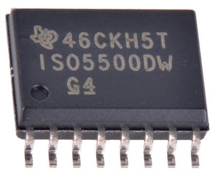
ICGOO电子元器件商城为您提供ISO5500DW由Texas Instruments设计生产,在icgoo商城现货销售,并且可以通过原厂、代理商等渠道进行代购。 ISO5500DW价格参考¥64.87-¥99.55。Texas InstrumentsISO5500DW封装/规格:隔离器 - 栅极驱动器, 2.5A Gate Driver Capacitive Coupling 4243Vrms 1 Channel 16-SOIC。您可以下载ISO5500DW参考资料、Datasheet数据手册功能说明书,资料中有ISO5500DW 详细功能的应用电路图电压和使用方法及教程。
ISO5500DW 是 Texas Instruments(德州仪器)生产的一款高性能双通道隔离式栅极驱动器,广泛应用于需要高压隔离和高效驱动能力的电力电子系统中。其主要应用场景包括:

1. 电机驱动与逆变器系统:用于驱动MOSFET或IGBT,广泛应用于工业电机控制、伺服驱动器和变频器中,提供高隔离电压和抗干扰能力。

2. 太阳能逆变器:在光伏逆变系统中,ISO5500DW 可靠地驱动功率开关器件,确保高压侧与低压侧的电气隔离,提高系统安全性和稳定性。

3. 电动汽车与充电桩:用于车载充电器、DC-DC转换器等高压系统中,实现对功率器件的高速、高可靠性驱动。

4. 工业电源与UPS系统:在不间断电源(UPS)和高压电源模块中,提供隔离驱动,增强系统的抗噪能力和安全性。

该器件具有高绝缘耐压(高达5kVRMS)、低传播延迟和快速驱动能力,适用于高频率开关应用。其双通道独立驱动设计,支持半桥或全桥拓扑结构,是高性能电力电子系统中的关键元件。
| 参数 | 数值 |
| 产品目录 | 集成电路 (IC)半导体 |
| 描述 | IC GATE DRVR IGBT/MOSFET 16SOIC门驱动器 2.5A Iso IGBT/MOSFET Gate Driver |
| 产品分类 | PMIC - MOSFET,电桥驱动器 - 外部开关集成电路 - IC |
| 品牌 | Texas Instruments |
| 产品手册 | http://www.ti.com/litv/sllse64c |
| 产品图片 |
|
| rohs | 符合RoHS无铅 / 符合限制有害物质指令(RoHS)规范要求 |
| 产品系列 | 电源管理 IC,门驱动器,Texas Instruments ISO5500DW- |
| 数据手册 | |
| 产品型号 | ISO5500DW |
| PCN设计/规格 | |
| 上升时间 | 55 ns |
| 下降时间 | 10 ns |
| 产品 | MOSFET Gate Drivers |
| 产品种类 | 门驱动器 |
| 供应商器件封装 | 16-SOIC |
| 其它名称 | 296-34888-5 |
| 制造商产品页 | http://www.ti.com/general/docs/suppproductinfo.tsp?distId=10&orderablePartNumber=ISO5500DW |
| 包装 | 管件 |
| 商标 | Texas Instruments |
| 安装类型 | 表面贴装 |
| 安装风格 | SMD/SMT |
| 封装 | Tube |
| 封装/外壳 | 16-SOIC(0.295",7.50mm 宽) |
| 封装/箱体 | SOIC-16 |
| 工作温度 | -40°C ~ 125°C |
| 工厂包装数量 | 40 |
| 延迟时间 | 200ns |
| 最大功率耗散 | 592 mW |
| 最大工作温度 | + 125 C |
| 最小工作温度 | - 40 C |
| 标准包装 | 40 |
| 激励器数量 | 1 Driver |
| 电压-电源 | 3 V ~ 5.5 V,15 V ~ 30 V |
| 电流-峰值 | 2.5A |
| 电源电压-最大 | 5.5 V |
| 电源电压-最小 | 3 V |
| 电源电流 | 8.5 mA |
| 类型 | Isolated Drivers |
| 系列 | ISO5500 |
| 输入类型 | 反相和非反相 |
| 输出数 | 1 |
| 输出电流 | 2.5 A |
| 输出端数量 | 1 Output |
| 配置 | 高端 |
| 配置数 | 1 |
| 高压侧电压-最大值(自举) | - |

.jpg)


- 商务部:美国ITC正式对集成电路等产品启动337调查
- 曝三星4nm工艺存在良率问题 高通将骁龙8 Gen1或转产台积电
- 太阳诱电将投资9.5亿元在常州建新厂生产MLCC 预计2023年完工
- 英特尔发布欧洲新工厂建设计划 深化IDM 2.0 战略
- 台积电先进制程称霸业界 有大客户加持明年业绩稳了
- 达到5530亿美元!SIA预计今年全球半导体销售额将创下新高
- 英特尔拟将自动驾驶子公司Mobileye上市 估值或超500亿美元
- 三星加码芯片和SET,合并消费电子和移动部门,撤换高东真等 CEO
- 三星电子宣布重大人事变动 还合并消费电子和移动部门
- 海关总署:前11个月进口集成电路产品价值2.52万亿元 增长14.8%


PDF Datasheet 数据手册内容提取
Product Sample & Technical Tools & Support & Folder Buy Documents Software Community ISO5500 SLLSE64D–SEPTEMBER2011–REVISEDJANUARY2015 ISO5500 2.5-A Isolated IGBT, MOSFET Gate Driver 1 Features 3 Description • 2.5-AMaximumPeakOutputCurrent The ISO5500 is an isolated gate driver for IGBTs and 1 MOSFETs with power ratings of up to I = 150 A and • DrivesIGBTsuptoI =150A,V =600V C C CE V = 600 V. Input TTL logic and output power stage CE • CapacitiveIsolatedFaultFeedback are separated by a capacitive, silicon dioxide (SiO ), 2 • CMOS/TTLCompatibleInputs isolation barrier. When used in conjunction with isolated power supplies, the device blocks high • 300-nsMaximumPropagationDelay voltage, isolates ground, and prevents noise currents • SoftIGBTTurnoff from entering the local ground and interfering with or • IntegratedFail-SafeIGBTProtection damagingsensitivecircuitry. – HighVCE(DESAT)Detection The device provides over-current protection (DESAT) – UndervoltageLockout(UVLO)ProtectionWith to an IGBT or MOSFET while an Undervoltage Hysteresis Lockout circuit (UVLO) monitors the output power supply to ensure sufficient gate drive voltage. If the • UserConfigurableFunctions output supply drops below 12 V, the UVLO turns the – Inverting,NoninvertingInputs power transistor off by driving the gate drive output to – Auto-Reset alogiclowstate. – Auto-Shutdown For a DESAT fault, the ISO5500 initiates a soft • WideV Range:3Vto5.5V shutdown procedure that slowly reduces the CC1 IGBT/MOSFET current to zero while preventing large • WideV Range:15Vto30V CC2 di/dt induced voltage spikes. A fault signal is then • OperatingTemperature: –40°Cto125°C transmitted across the isolation barrier, actively • Wide-BodySO-16Package driving the open-drain FAULT output low and disabling the device inputs. The inputs are blocked as • ±50-kV/usTransientImmunityTypical long as the FAULT-pin is low. FAULT remains low • SafetyandRegulatoryApprovals: until the inputs are configured for an output low state, – VDE6000V BasicIsolationperDINVVDE followedbyalogiclowinputontheRESETpin. PK V0884-10(VDEV0884-10)andDINEN The ISO5500 is available in a 16-pin SOIC package 61010-1 and is specified for operating temperatures from – 4243V IsolationforOneMinuteperUL –40°Cto125°C. RMS 1577 DeviceInformation(1) – CSAComponentAcceptanceNotice#5A,IEC 61010-1,andIEC60950-1EndEquipment PARTNUMBER PACKAGE BODYSIZE(NOM) Standards ISO5500 SOIC(16) 10.30mm×7.50mm (1) For all available packages, see the orderable addendum at 2 Applications theendofthedatasheet. • IsolatedIGBTandMOSFETDrivesin FunctionalBlockDiagram – MotorControl – MotionControl VCC1 VREG ISO5500 – IndustrialInverters – Switched-ModePowerSupplies VIN+ +-UVLO VVCCC2 VIN- DELAY Barrier DGarnaivdtee +-DESAT 12.3V DESAT FAULT ISO- LFoaguilct 7.2V Q4 Q1b Q1a VOUT QS VE R RESET Q3 Q2b Q2a GND1 VEE-P VEE-L 1 An IMPORTANT NOTICE at the end of this data sheet addresses availability, warranty, changes, use in safety-critical applications, intellectualpropertymattersandotherimportantdisclaimers.PRODUCTIONDATA.
ISO5500 SLLSE64D–SEPTEMBER2011–REVISEDJANUARY2015 www.ti.com Table of Contents 1 Features.................................................................. 1 8.3 FeatureDescription.................................................17 2 Applications........................................................... 1 8.4 DeviceFunctionalModes........................................25 3 Description............................................................. 1 9 ApplicationandImplementation........................ 26 4 RevisionHistory..................................................... 2 9.1 ApplicationInformation............................................26 9.2 TypicalApplication .................................................26 5 PinConfigurationandFunctions......................... 3 10 PowerSupplyRecommendations..................... 35 6 Specifications......................................................... 4 11 Layout................................................................... 35 6.1 AbsoluteMaximumRatings......................................4 6.2 ESDRatings..............................................................4 11.1 LayoutGuidelines.................................................35 6.3 RecommendedOperatingConditions.......................4 11.2 PCBMaterial.........................................................35 6.4 ThermalInformation..................................................5 11.3 LayoutExample....................................................35 6.5 ElectricalCharacteristics...........................................5 12 DeviceandDocumentationSupport................. 36 6.6 SwitchingCharacteristics..........................................6 12.1 DeviceSupport......................................................36 6.7 TypicalCharacteristics..............................................7 12.2 DocumentationSupport........................................36 7 ParameterMeasurementInformation................12 12.3 Trademarks...........................................................36 12.4 ElectrostaticDischargeCaution............................36 8 DetailedDescription............................................ 16 13 Mechanical,Packaging,andOrderable 8.1 Overview.................................................................16 Information........................................................... 36 8.2 FunctionalBlockDiagram.......................................16 4 Revision History ChangesfromRevisionC(June2013)toRevisionD Page • AddedPinConfigurationandFunctionssection,ESDRatingstable,FeatureDescriptionsection,DeviceFunctional Modes,ApplicationandImplementationsection,PowerSupplyRecommendationssection,Layoutsection,Device andDocumentationSupportsection,andMechanical,Packaging,andOrderableInformationsection .............................. 1 • VDEstandardchangedtoDINVVDEV0884-10(VDEV0884-10):2006-12...................................................................... 1 • AddedFAULTlimitstoAbsoluteMaximumRatings.............................................................................................................. 4 ChangesfromRevisionB(May2013)toRevisionC Page • ChangedV from1200Vto600V........................................................................................................................................ 1 CE • AddedtheThermalInformationtableinsidethedatasheetbelowtheAbsoluteMaximumRatingstable............................ 5 • ChangedrowV andV specificationfromV of1200V to680V ....................................................................... 17 IORM PR IORM pk pk • Changed1200V intheRegulatoryInformationtablefrom1200V to680V ............................................................. 17 PK PK PK • DeletedlastrowoftheIEC60664-1RatingTable............................................................................................................... 18 • AddedIsolationLifetimeataMaximumContinuousWorkingVoltagetable........................................................................ 18 • AddedFunctionTableundertheFunctionalBlockDiagram................................................................................................ 25 ChangesfromRevisionA(July2012)toRevisionB Page • ChangedtheRegulatoryApprovalsList................................................................................................................................. 1 • ChangedtheREGULATORYINFORMATIONtable,VDEColumnFrom:FileNumber:pendingTo:FileNumber: 40016131.............................................................................................................................................................................. 17 • ChangedtheREGULATORYINFORMATIONtable,CSAColumnFrom:FileNumber:pendingTo:FileNumber: 220991.................................................................................................................................................................................. 17 ChangesfromOriginal(September2011)toRevisionA Page • ChangedthedeviceFrom:ProductPreviewTo:Production................................................................................................. 1 2 SubmitDocumentationFeedback Copyright©2011–2015,TexasInstrumentsIncorporated ProductFolderLinks:ISO5500
ISO5500 www.ti.com SLLSE64D–SEPTEMBER2011–REVISEDJANUARY2015 5 Pin Configuration and Functions DWPackage 16-PinSOIC TopView V 1 16 V IN+ E V 2 15 V IN- EE-L V 3 14 DESAT CC1 N O GND1 4 TI 13 VCC2 A RESET 5 OL 12 VC FAULT 6 S 11 V I OUT NC 7 10 V EE-L GND1 8 9 V EE-P PinFunctions PIN I/O DESCRIPTION NO. NAME 1 V I Noninvertinggatedrivevoltagecontrolinput IN+ 2 V I Invertinggatedrivevoltagecontrolinput IN– 3 V Supply Positiveinputsupply(3Vto5.5V) CC1 4,8 GND1 Ground Inputground 5 RESET I FAULTresetinput 6 FAULT O Open-drainoutput.Connectto3.3kpullupresistor 7 NC NC Notconnected 9 V Supply Mostnegativeoutput-supplypotentialofthepoweroutput.Connectexternallytopin10. EE-P Mostnegativeoutput-supplypotentialofthelogiccircuitry.Pin10and15areinternallyconnected. 10,15 V Supply EE-L Connectatleastpin10externallytopin9.Pin15canbefloating. 11 V O Gatedriveoutputvoltage OUT 12 V Supply Gatedriversupply.ConnecttoV . C CC2 13 V Supply Mostpositiveoutputsupplypotential CC2 14 DESAT I Desaturationvoltageinput 16 V Ground Gatedrivecommon.ConnecttoIGBTEmitter. E Copyright©2011–2015,TexasInstrumentsIncorporated SubmitDocumentationFeedback 3 ProductFolderLinks:ISO5500
ISO5500 SLLSE64D–SEPTEMBER2011–REVISEDJANUARY2015 www.ti.com 6 Specifications 6.1 Absolute Maximum Ratings overoperatingfree-airtemperaturerange(unlessotherwisenoted) MIN MAX UNIT Supplyvoltage,V –0.5 6 V CC1 Totaloutputsupplyvoltage,V (V –V ) –0.5 35 V OUT(total) CC2 EE-P 35– Positiveoutputsupplyvoltage,V (V –V ) –0.5 V OUT+ CC2 E (V –V ) E EE-P Negativeoutputsupplyvoltage,V (V –V ) –0.5 V V OUT- E EE-P CC2 DESAT V –0.5 V E CC2 Voltageat V V ,V ,RESET,FAULT –0.5 6 IN+ IN– Peakgatedriveoutputvoltage V –0.5 V V o(peak) CC2 Collectorvoltage,V –0.5 V V C CC2 Outputcurrent,I (1) ±2.8 A O FAULToutputcurrent,I ±20 mA FL Maximumjunctiontemperature,T 170 °C J Storagetemperature,T –65 150 °C stg (1) Maximumpulsewidth=10μs,maximumdutycycle=0.2%. 6.2 ESD Ratings VALUE UNIT Humanbodymodel(HBM),perANSI/ESDA/JEDECJS-001(1) ±4000 Charged-devicemodel(CDM),perJEDECspecificationJESD22- ±1500 V(ESD) Electrostaticdischarge C101(2) V MachinemodelJEDECJESD22-A115-A ±200 (1) JEDECdocumentJEP155statesthat500-VHBMallowssafemanufacturingwithastandardESDcontrolprocess. (2) JEDECdocumentJEP157statesthat250-VCDMallowssafemanufacturingwithastandardESDcontrolprocess. 6.3 Recommended Operating Conditions overoperatingfree-airtemperaturerange(unlessotherwisenoted) MIN NOM MAX UNIT V Supplyvoltage 3 5.5 V CC1 V Totaloutputsupplyvoltage(V –V ) 15 30 V OUT(total) CC2 EE-P 30–(V – V V Positiveoutputsupplyvoltage(V –V ) 15 E OUT+ CC2 E V ) EE-P V Negativeoutputsupplyvoltage(V –V ) 0 15 V OUT– E EE-P V Collectorvoltage V +8 V V C EE-P CC2 t Inputpulsewidth 0.1 μs ui t RESETInputpulsewidth 0.1 μs uiR V High-levelinputvoltage(V ,V ,RESET) 2 V V IH IN+ IN– CC V Low-levelinputvoltage(V ,V ,RESET) 0 0.8 V IL IN+ IN– f Inputfrequency 520(1) kHz INP V SupplySlewRate(V orV –V )(2) 75 V/ms SUP_SR CC1 CC2 EE-P T Junctiontemperature –40 150 °C J T Ambienttemperature -40 25 125 °C A (1) IfT =125°C,V =5.5V,V =30V,R =10Ω,C =1nF A CC1 CC2 G L (2) IfV skewisfasterthan75V/ms(especiallyforthefallingedge)thenV mustbepoweredupafterV andpowereddownbefore CC1 CC2 CC1 V toavoidoutputglitches. CC1 4 SubmitDocumentationFeedback Copyright©2011–2015,TexasInstrumentsIncorporated ProductFolderLinks:ISO5500
ISO5500 www.ti.com SLLSE64D–SEPTEMBER2011–REVISEDJANUARY2015 6.4 Thermal Information ISO5500 THERMALMETRIC(1) DW(SOIC)16 UNIT PINS θ Junction-to-ambientthermalresistance 76 JA θ Junction-to-case(top)thermalresistance 34 JCtop θ Junction-to-boardthermalresistance 36 °C/W JB ψ Junction-to-topcharacterizationparameter 8 JT ψ Junction-to-boardcharacterizationparameter 35 JB T 185 °C SHDN+ ThermalShutdown T 173 °C SHDN- T ThermalShutdownHysteresis 12 °C SHDN-HYS P PowerDissipationSeeEquation2throughEquation6 592 mW D (1) Formoreinformationabouttraditionalandnewthermalmetrics,seetheICPackageThermalMetricsapplicationreport,SPRA953. 6.5 Electrical Characteristics AlltypicalvaluesareatT =25°C,V =5V,V –V =30V,V –V =0V(unlessotherwisenoted) A CC1 CC2 E E EE-P PARAMETER TESTCONDITIONS MIN TYP MAX UNIT ICC1 Supplycurrent Q30u0ieksHceznt VFiIg=urVeC2C,1Foirg0urVe,2N8o,alonaddF,iSgeuereF2ig9ure1, 55..57 88..57 mA ICC2 Supplycurrent Q30u0ieksHceznt VthIr=ouVgChCF1iogru0reV5,,NFoigluoraed3,0S,eaenFdigFuigreur3e31 8.49 1124 mA IOUT=0,SeeFigure27andFigure30 1.3 ICH High-levelcollectorcurrent mA IOUT=–650μA,SeeFigure27andFigure30 1.9 ICL Low-levelcollectorcurrent SeeFigure27andFigure31 0.4 mA IEH VEHigh-levelsupplycurrent SeeFigure6andFigure40 –0.5 –0.3 mA IEL VELow-levelsupplycurrent SeeFigure6andFigure41 –0.8 –0.53 mA IIH High-levelinputleakage 10 INfrom0toVCC μA IIL Low-levelinputleakage –10 IFH High-levelFAULTpinoutputcurrent VSFeAeUFLTig=urVeC3C31,nopull-up, –10 10 μA IFL Low-levelFAULTpinoutputcurrent VFAULT=0.4V,nopull-up,SeeFigure34 5 12 mA VIT+(UVLO) Positive-goingUVLOthresholdvoltage 11.6 12.3 13.5 VIT–(UVLO) Negative-goingUVLOthresholdvoltage SeeFigure32 11.1 12.4 V VHYS(UVLO) UVLOHysteresisvoltage(VIT+–VIT–) 0.7 1.2 VOUT=VCC2–4V(1),SeeFigure7and –1 –1.6 Figure35 IOH High-leveloutputcurrent VOUT=VCC2–15V(2),SeeFigure7and –2.5 A Figure35 VOUT=VEE-P+2.5V(1),SeeFigure8and 1 1.8 Figure36 IOL Low-leveloutputcurrent VOUT=VEE-P+15V(2),SeeFigure8and 2.5 A Figure36 IOF Output-lowfaultcurrent VFiOgUuTre–3V7EE-P=14V,SeeFigure9and 90 140 230 mA IaOnUdTF=ig–u1r0e03m8A,SeeFigure10,Figure11 VC-1.5 VC-0.8 VOH High-leveloutputvoltage V IFOiUgTur=e–36850μA,SeeFigure10,Figure11and VC-0.15 VC-0.05 VOL Low-leveloutputvoltage IFOiUgTur=e13090mA,SeeFigure12,Figure13and 0.2 0.5 V ICHG Blankingcapacitorchargingcurrent VFiDgEuSrAeT4=20Vto6V,SeeFigure14and –180 –270 –380 μA IDSCHG Blankingcapacitordischargecurrent VDESAT=8V,SeeFigure42 20 45 mA (1) Maximumpulsewidthis50μs,maximumdutycycleis0.5% (2) Maximumpulsewidthis10μs,maximumdutycycleis0.2% Copyright©2011–2015,TexasInstrumentsIncorporated SubmitDocumentationFeedback 5 ProductFolderLinks:ISO5500
ISO5500 SLLSE64D–SEPTEMBER2011–REVISEDJANUARY2015 www.ti.com Electrical Characteristics (continued) AlltypicalvaluesareatT =25°C,V =5V,V –V =30V,V –V =0V(unlessotherwisenoted) A CC1 CC2 E E EE-P PARAMETER TESTCONDITIONS MIN TYP MAX UNIT VDSTH DESATthresholdvoltage (FVigCuCr2e–4V2E)>VTH-(UVLO),SeeFigure15and 6.7 7.2 7.7 V CMTI Commonmodetransientimmunity VI=VCC1or0V,VCMat1500V, 25 50 kV/μS SeeFigure43thoughFigure46 6.6 Switching Characteristics AlltypicalvaluesareatT =25°C,V =5V,V –V =30V,V –V =0V(unlessotherwisenoted) A CC1 CC2 E E EE-P PARAMETER TESTCONDITIONS MIN TYP MAX UNIT t ,t PropagationDelay 150 200 300 ns PLH PHL R =10Ω,C =10nF, G G tsk-p PulseSkew|tPHL–tPLH| 50%dutycycle,10kHzinput, 1.7 10 ns tsk-pp Part-to-partskew(1) VCC2–VEE=30V, 45 ns V –V =0V,SeeFigure16 t Part-to-partskew(2) E EE –50 50 ns sk2-pp throughFigure19,Figure26, t Outputsignalrisetime Figure47,Figure49,and 55 ns r Figure50 t Outputsignalfalltime 10 ns f t DESATsenseto90%VOUTdelay 300 550 ns DESAT(90%) tDESAT(10%) DESATsenseto10%VOUTdelay RG=10Ω,CG=10nF, 1.8 2.3 μs V –V =30V, t DESATsensetoFAULTlowoutputdelay CC2 EE-P 290 550 ns DESAT(FAULT) V –V =0V,SeeFigure20 E EE-P DESATsensetoDESATlowpropagation throughFigure25,Figure48and t 180 ns DESAT(LOW) delay Figure51 t RESETtohigh-levelFAULTsignaldelay 3 8.2 13 μs RESET(FAULT) t UVLOtoV highdelay 1msrampfrom0Vto30V 4 μs UVLO(ON) OUT t UVLOtoV lowdelay 1msrampfrom30Vto0V 6 μs UVLO(OFF) OUT Failsafeoutputdelaytimefrominputpower t 2.8 μs FS loss (1) t isthemaximumdifferenceinsameedgepropagationdelaytimes(eitherV toV orV toV )betweentwodevices sk-pp IN+ OUT IN– OUT operatingatthesamesupplyvoltage,sametemperature,andhavingidenticalpackagesandtestcircuits. i.e.max ìïéëtPHL-max(VCC1,VCC2,TA) - tPHL-min(VCC1,VCC2,TA)ùû,ïü í ý ïîëétPLH-max(VCC1,VCC2,TA) - tPLH-min(VCC1,VCC2,TA)ûùïþ (2) t isthepropagationdelaydifferenceinhigh-to-lowtolow-to-hightransition(anyofthecombinationsV toV orV toV ) sk2-pp IN+ OUT IN– OUT betweentwodevicesoperatingatthesamesupplyvoltage,sametemperature,andhavingidenticalpackagesandtestcircuits. i.e. min=t (V V T ) - t (V V T ) PHL-min CC1, CC2, A PLH-max CC1, CC2, A max=t (V V T ) - t (V V T ) PHL-max CC1, CC2, A PLH-min CC1, CC2, A 6 SubmitDocumentationFeedback Copyright©2011–2015,TexasInstrumentsIncorporated ProductFolderLinks:ISO5500
ISO5500 www.ti.com SLLSE64D–SEPTEMBER2011–REVISEDJANUARY2015 6.7 Typical Characteristics 8 7 7 A) A) 6 m 6 m nt ( nt ( 5 e 5 e urr urr C C y 4 y 4 pl pl p p u 3 u S S 3 - - C1 2 C1 IC 1 VVCCCC11== 33 .V3 V VVCCCC11== 45. 5V V IC 2 VCC1= 3.3 V VCC1= 3.6 V VCC1= 5.5 V VCC1= 5 V 0 1 -40 -20 0 20 40 60 80 100 120 140 0 50 100 150 200 250 300 AmbientTemperature (oC) Input Frequency (KHz) Figure1.V SupplyCurrentvs.Temperature Figure2.V SupplyCurrentvs.Frequency CC1 CC1 12 12 No Load 11 A) A) 11 m 10 m nt ( nt ( 10 e 9 e urr urr C C y 8 y 9 pl pl p p u 7 u S S 8 - - C2 6 C2 IC 5 VVCCCC22== 1250 VV IC 7 VVCCCC22== 1250 VV VCC2= 30 V VCC2= 30 V 4 6 -40 -20 0 20 40 60 80 100 120 140 0 50 100 150 200 250 300 AmbientTemperature (oC) Input Frequency (KHz) Figure3.V SupplyCurrentvs.Temperature Figure4.V SupplyCurrentvs.Frequency CC2 CC2 70 0 RG= 10W 60 fINP= 20 kHz A) -0.1 A) m urrent (m 4500 Current ( --00..32 C y y pl -0.4 Suppl 30 - Sup -0.5 I- CC2 1200 VCC2= 15 V I, IEHEL--00..76 IIIEEEHHL,,, VVVEEE--- VVVEEEEEE=== 001 5VV V 0 VCC2= 30 V -0.8 IEL, VE- VEE= 15 V 0 20 40 60 80 100 -40 -20 0 20 40 60 80 100 120 140 Load Capacitance (nF) AmbientTemperature (oC) Figure5.VCC2SupplyCurrentvs.LoadCapacitance Figure6.VESupplyCurrentvs.Temperature Copyright©2011–2015,TexasInstrumentsIncorporated SubmitDocumentationFeedback 7 ProductFolderLinks:ISO5500
ISO5500 SLLSE64D–SEPTEMBER2011–REVISEDJANUARY2015 www.ti.com Typical Characteristics (continued) 0 8 VOUT= 2.5 V ve Current (A)--01-..-5521 k Current (A) 576 VOUT= 15 V Dri-2.5 Sin 4 Output -3-.53 Output 3 - - 2 H -4 L O O I-4.5 VOUT= VC- 4 V I 1 VOUT= VC- 15 V -5 0 -40 -20 0 20 40 60 80 100 120 140 -40 -20 0 20 40 60 80 100 120 140 AmbientTemperature (oC) AmbientTemperature (oC) Figure7.OutputDriveCurrentvs.Temperature Figure8.OutputSinkCurrentvs.Temperature 160 0.1 V) g 150 p ( -0.1 n o I- Output Sink Current DuriOFa Fault Condition (mA) 1111130241890000000 TTTAAA=== -2145205oCooCC -- HiVgh Output Voltage DrOHC-------1000011.......5593731 IIOOUUTT== --615000 mmAA V 0 5 10 15 20 25 30 -40 -20 0 20 40 60 80 100 120 140 Output Voltage (V) AmbientTemperature (oC) Figure9.OutputSinkCurrentDuringaFaultCondition Figure10.HighOutputVoltageDropvs.Temperature vs.OutputVoltage 30 0.35 29.5 TTAA== -2450oCoC IOUT= 100 mA Output Voltage (V) 2278222..55897 TA= 125oC Output Voltage (V) 0.002..532 High 26.5 Low V- OH 252.56 V- OL 0.15 25 0.1 0 0.2 0.4 0.6 0.8 1 1.2 1.4 1.5 -40 -20 0 20 40 60 80 100 120 140 Output DriveCurrent(A) AmbientTemperature (oC) Figure11.HighOutputVoltagevs.OutputDriveCurrent Figure12.LowOutputVoltagevs.Temperature 8 SubmitDocumentationFeedback Copyright©2011–2015,TexasInstrumentsIncorporated ProductFolderLinks:ISO5500
ISO5500 www.ti.com SLLSE64D–SEPTEMBER2011–REVISEDJANUARY2015 Typical Characteristics (continued) 6 -0.15 g -0.17 n 5 gi w Output Voltage (V) 342 nking Capacitor CharCurrent (mA) ------000000......221222599371 o a V- LOL 1 TTAA== -2450oCoC - BlCHG --00..3331 0 TA= 125oC I -0.35 0 0.5 1 1.5 2 2.5 -40 -20 0 20 40 60 80 100 120 140 Output Sink Current (A) AmbientTemperature (oC) Figure13.LowOutputVoltagevs.OutputSinkCurrent Figure14.BlankingCapacitanceChargingCurrentvs. Temperature 7.9 240 RG= 10W, V) 7.7 230 CL= 10 nF atThreshold ( 77..53 n Delay (ns) 222100 Des 7.1 atio V- DSTH 66..97 Propag 210900 tttPPPLHLHHLaaattt VVVCCCCCC111=== 33 5.. 33V VV tPHLat VCC1= 5 V 6.5 180 -40 -20 0 20 40 60 80 100 120 140 -40 -20 0 20 40 60 80 100 120 140 AmbientTemperature (oC) AmbientTemperature (oC) Figure15.DESATThresholdvs.Temperature Figure16.PropagationDelayvs.Temperature 225 230 RG= 10W, RG= 10W, CL= 10 nF 225 CL= 10 nF 220 s) s) 220 n n y ( y ( 215 a 215 a el el n D n D 210 o o ati 210 ati 205 g g a a p p Pro 205 Pro 200 ttPPLHHLaatt VVCCCC11== 33..33 VV tPLH 195 tPLHat VCC1= 5 V tPHL tPHLat VCC1= 5 V 200 190 3 3.5 4 4.5 5 5.5 14 16 18 20 22 24 26 28 30 V Supply Voltage (V) V Supply Voltage (V) CC1 CC2 Figure17.PropagationDelayvs.V SupplyVoltage Figure18.PropagationDelayvs.V SupplyVoltage CC1 CC2 Copyright©2011–2015,TexasInstrumentsIncorporated SubmitDocumentationFeedback 9 ProductFolderLinks:ISO5500
ISO5500 SLLSE64D–SEPTEMBER2011–REVISEDJANUARY2015 www.ti.com Typical Characteristics (continued) 1400 450 RG= 10W s) RG= 10W, 1200 y (n 400 CL= 10 nF a elay (ns) 1080000 VDelOUT 350 D Propagation 6240000000 ttttPPPPLHLHHHLLaaaatttt VVVVCCCCCCCC1111==== 3355.. 33VV VV Desat Sense to 90% 221305500000 VVCCCC22== 1350 VV 0 10 20 30 40 50 60 70 80 90 100 -40 -20 0 20 40 60 80 100 120 140 Load Capacitance (nF) AmbientTemperature (oC) Figure19.PropagationDelayvs.LoadCapacitance Figure20.DESATSenseto90%V DelayvsTemperature OUT 1600 2.5 s) RG= 10W s) RG= 10W, n1400 m ay ( ay ( 2 CL= 10 nF el1200 el D D T T OU1000 OU 1.5 V V % 800 % 0 0 o 9 600 o 1 1 e t e t s s n 400 n Se Se 0.5 Desat 2000 VVCCCC22== 1350 VV Desat 0 VVCCCC22== 1350 VV 0 10 20 30 40 50 60 70 80 90 100 -40 -20 0 20 40 60 80 100 120 140 Load Capacitance (nF) AmbientTemperature (oC) Figure21.DESATSenseto90%V DelayvsLoad Figure22.DESATSenseto10%V DelayvsTemperature OUT OUT Capacitance 18 450 elay (s)m 1154 RG= 10W ay (ns) 400 D el UT 12 w D 350 O o V 10 L % ult 300 10 8 Fa o o e t 6 e t 250 ns ns e 4 e Desat S 02 VVCCCC22== 1350 VV Desat S 210500 VVCCCC22== 1350 VV 0 10 20 30 40 50 60 70 80 90 100 -40 -20 0 20 40 60 80 100 120 140 Load Capacitance (nF) AmbientTemperature (oC) Figure23.DESATSenseto10%V DelayvsLoad Figure24.DESATSensetoFaultLowDelayvsTemperature OUT Capacitance 10 SubmitDocumentationFeedback Copyright©2011–2015,TexasInstrumentsIncorporated ProductFolderLinks:ISO5500
ISO5500 www.ti.com SLLSE64D–SEPTEMBER2011–REVISEDJANUARY2015 Typical Characteristics (continued) 10 9.5 VCC2- VEE= 30 V 9 RG= 0W, s) CL= 10 nF y (m 8.5 ela 8 D ult 7.5 a o F 7 VCC1= 3 V Reset t 6.56 VVVCCCCCC111=== 334...365 VVV V / div 5.5 VCC1= 5 V 5 5 VCC1= 5.5 V -40 -20 0 20 40 60 80 100 120 140 AmbientTemperature (oC) Time 125 ns / div Figure25.ResettoFaultDelayvsTemperature Figure26.OutputWaveform 3 A) m 2.5 nt ( urre 2 C y pl 1.5 p u S - L 1 ICH, IOUT= -500mA , IHC IICCHL,, IIOOUUTT== --11 mmAA IC 0.5 ICL, IOUT= -2 mA 0 -40 -20 0 20 40 60 80 100 120 140 AmbientTemperature (oC) Figure27.V SupplyCurrentvs.Temperature C Copyright©2011–2015,TexasInstrumentsIncorporated SubmitDocumentationFeedback 11 ProductFolderLinks:ISO5500
ISO5500 SLLSE64D–SEPTEMBER2011–REVISEDJANUARY2015 www.ti.com 7 Parameter Measurement Information 1 1 VIN+ VE 16 VIN+ VE 16 5.5V 0µ.F1 ICC1 2 VIN- VEE-L 15 5.5V 0µ.F1 ICC1 2 VIN- VEE-L 15 3 3 VCC1 DESAT 14 VCC1 DESAT 14 4 4 GND1 VCC2 13 GND1 VCC2 13 5 5 RESET VC 12 RESET VC 12 6 6 FAULT VOUT 11 FAULT VOUT 11 7 7 NC VEE-L 10 NC VEE-L 10 8 8 GND1 VEE-P 9 GND1 VEE-P 9 Figure28.I TestCircuit Figure29.I TestCircuit CC1H CC1L 1 16 16 VIN+ VE 1 VIN+ VE 5V 0µ.F1 2 VIN- VEE-L 15 2 VIN- VEE-L 15 3 14 14 VCC1 DESAT 3 VCC1 DESAT ICC2 ICC2 4 13 13 GND1 VCC2 4 GND1 VCC2 IC IC 5 12 12 RESET VC 5 RESET VC 30V 6 FAULT VOUT 11 0µ.1F 6 FAULT VOUT 11 30V 0µ.F1 7 NC VEE-L 10 IOUT 7 NC VEE-L 10 8 9 9 GND1 VEE-P 8 GND1 VEE-P Figure30. I ,I TestCircuit Figure31.I ,I TestCircuit CC2H CH CC2L CL 1 16 1 16 VIN+ VE VIN+ VE 5V 0µ.F1 2 VIN- VEE-L 15 0µ.F1 5.5V 0µ.F1 2 VIN- VEE-L 15 3 VCC1 DESAT 14 SwVe1ep 3 VCC1 DESAT 14 4 13 0.1 4 13 GND1 VCC2 µF GND1 VCC2 5 12 5 12 RESET VC V2 RESET VC 6 FAULT VOUT 11 VOUT 0µ.F1 5.5VIFAULT 6 FAULT VOUT 11 30V 0µ.F1 7 10 7 10 NC VEE-L NC VEE-L 8 9 8 9 GND1 VEE-P GND1 VEE-P Figure32.V TestCircuit Figure33.I TestCircuit IT(UVLO) FH 12 SubmitDocumentationFeedback Copyright©2011–2015,TexasInstrumentsIncorporated ProductFolderLinks:ISO5500
ISO5500 www.ti.com SLLSE64D–SEPTEMBER2011–REVISEDJANUARY2015 Parameter Measurement Information (continued) 1 16 1 16 VIN+ VE VIN+ VE 3V 0µ.F1 2 VIN- VEE-L 15 5V 0µ.F1 2 VIN- VEE-L 15 3 14 3 14 VCC1 DESAT VCC1 DESAT 4 13 4 13 VPULSE GND1 VCC2 GND1 VCC2 5 12 5 12 RESET VC RESET VC 0.1 4.7 0.4V IFAULT 67 FAULT VOUT 1110 30V 0µ.F1 67 FAULT VOUT 1110 IOUT 30V µF µF NC VEE-L NC VEE-L 8 9 8 9 GND1 VEE-P GND1 VEE-P Figure34.I TestCircuit Figure35.I TestCircuit FL OH 16 1 16 1 VIN+ VE VIN+ VE 2 VIN- VEE-L 15 5V 0µ.F1 2 VIN- VEE-L 15 14 3 14 3 VCC1 DESAT VCC1 DESAT 13 4 13 4 GND1 VCC2 GND1 VCC2 12 5 12 0.1 5 RESET VC 30V 0.1 4.7 RESET VC µF 30V 11 VPULSE µF µF 6 11 IOUT 6 FAULT VOUT FAULT VOUT 7 NC VEE-L 10 IOUT 7 NC VEE-L 10 14V 9 8 9 8 GND1 VEE-P GND1 VEE-P Figure36.I TestCircuit Figure37.I TestCircuit OL OF 1 16 1 16 VIN+ VE VIN+ VE 5V 0µ.F1 2 VIN- VEE-L 15 5V 0µ.F1 2 VIN- VEE-L 15 3 14 3 14 VCC1 DESAT VCC1 DESAT 4 13 4 13 GND1 VCC2 GND1 VCC2 5 RESET VC 12 VOUT 0µ.F1 30V 5 RESET VC 12 1m0A0 0µ.F1 30V 6 11 6 11 FAULT VOUT FAULT VOUT VOUT 7 10 7 10 NC VEE-L IOUT NC VEE-L 8 9 8 9 GND1 VEE-P GND1 VEE-P Figure38.V TestCircuit Figure39.V TestCircuit OH OL Copyright©2011–2015,TexasInstrumentsIncorporated SubmitDocumentationFeedback 13 ProductFolderLinks:ISO5500
ISO5500 SLLSE64D–SEPTEMBER2011–REVISEDJANUARY2015 www.ti.com Parameter Measurement Information (continued) 1 16 IE 1 16 IE VIN+ VE VIN+ VE 5V 0µ.F1 2 VIN- VEE-L 15 0µ.F1 5V 0µ.F1 2 VIN- VEE-L 15 0µ.F1 3 14 3 14 VCC1 DESAT V1 VCC1 DESAT V1 4 13 0.1 4 13 0.1 GND1 VCC2 µF GND1 VCC2 µF 5 12 5 12 RESET VC V2 RESET VC V2 0.1 0.1 6 FAULT VOUT 11 µF 6 FAULT VOUT 11 µF 7 10 7 10 NC VEE-L NC VEE-L 8 9 8 9 GND1 VEE-P GND1 VEE-P Figure40.I TestCircuit Figure41.I TestCircuit EH EL 1 16 1 16 VIN+ VE VIN+ VE 5V 0µ.F1 2 VIN- VEE-L 15SWEEP 0µ.F1 5V 0µ.F1 2 VIN- VEE-L 15 3 VCC1 DESAT 14 V1 3 VCC1 DESAT 14 IDESAT 4 GND1 VCC2 13 0µ.F1 4 GND1 VCC2 13 5 RESET VC 12 V2 3k 5 RESET VC 12 0.1 0.1 4.7 30V 6 FAULT VOUT 11 µF SCOPE 6 FAULT VOUT 11 µF µF 7 NC VEE-L 10 100pF 7 NC VEE-L 10 10W 8 GND1 VEE-P 9 8 GND1 VEE-P 9 10 nF VCM Figure42.I ,I ,V TestCircuit Figure43.CMTIV TestCircuit CHG DSCHG DSTH FH 1 16 1 16 VIN+ VE VIN+ VE 5V 0µ.F1 2 VIN- VEE-L 15 5V 0µ.F1 2 VIN- VEE-L 15 3 14 3 14 VCC1 DESAT VCC1 DESAT 4 13 4 13 GND1 VCC2 GND1 VCC2 5 12 5 12 3k RESET VC 3k RESET VC SCOPE 0.1 4.7 30V 0.1 4.7 30V SCOPE 6 FAULT VOUT 11 µF µF 6 FAULT VOUT 11 µF µF 100pF 7 NC VEE-L 10 10W 100pF 7 NC VEE-L 10 10W 8 9 8 9 GND1 VEE-P 10 GND1 VEE-P 10 nF nF VCM VCM Figure44.CMTIV TestCircuit Figure45.CMTIV TestCircuit FL OH 14 SubmitDocumentationFeedback Copyright©2011–2015,TexasInstrumentsIncorporated ProductFolderLinks:ISO5500
ISO5500 www.ti.com SLLSE64D–SEPTEMBER2011–REVISEDJANUARY2015 Parameter Measurement Information (continued) 1 16 1 16 VIN+ VE VIN VIN+ VE 5V 0µ.F1 2 VIN- VEE-L 15 GND1 2 VIN- VEE-L 15 3 VCC1 DESAT 14 3 VCC1 DESAT 14 4 GND1 VCC2 13 4 GND1 VCC2 13 3k 56 RFAEUSLETT VOVUTC 1112 SCOPE 0µ.F1 4µ.F7 30V 5V 0µ.F1 3k 56 FRAEUSLETT VOVUTC 1112 VOUT V1 0µ.F1 4µ.F7 10W 100pF 7 NC VEE-L 10 10W 7 NC VEE-L 10 10 nF 8 GND1 VEE-P 9 10 8 GND1 VEE-P 9 nF VCM Figure46.CMTIV TestCircuit Figure47.t ,t ,t,t TestCircuit OL PLH PHL r f VIN- 0V 1 16 VIN 2 VVIINN+- VEEV-EL 15 1p0F0 0µ.F1 3 VCC1 DESAT 14 V1 0.1 VIN+ 50% 50% DESAT µF 4 GND1 VCC2 13 tr tf 5 12 VOUT RESET VC 0µ.F1 4µ.F7 V2 90% 6 11 5V 3k FAULT VOUT 10W 50% 7 10 0.1 NC VEE-L 10 VOUT 10% µF 8 9 nF GND1 VEE-P tPLH tPHL Figure48.t ,t TestCircuit Figure49.V PropagationDelay,Non-inverting DESAT RESET OUT Configuration A. VIN- tDESAT(FAULT) tDESAT(10%) 50% 50% 7.2V tDESAT(LOW) VIN+ VCC1 VDESAT 50% tDESAT(90%) tr tf VOUT 90% 10% 90% FAULT 50% 50% 50% tRESET(FAULT) VOUT 10% RESET 50% tPLH tPHL Figure50.V PropagationDelay,Inverting Figure51.DESAT,V ,FAULT,RESETDelays OUT OUT Configuration Copyright©2011–2015,TexasInstrumentsIncorporated SubmitDocumentationFeedback 15 ProductFolderLinks:ISO5500
ISO5500 SLLSE64D–SEPTEMBER2011–REVISEDJANUARY2015 www.ti.com 8 Detailed Description 8.1 Overview TheISO5500isanisolatedgatedriverforIGBTsandMOSFETswithpowerratingsofuptoIC=150AandVCE = 600 V. Input TTL logic and output power stage are separated by a capacitive, silicon dioxide (SiO2), isolation barrier. The IO circuitry on the input side interfaces with a micro controller and consists of gate drive control and RESET inputs, and FAULT alarm output. The power stage consists of power transistors to supply 2.5 A pullup and pulldown currents to drive the capacitive load of the external power transistors, as well as DESAT detection circuitry to monitor IGBT collector-emitter overvoltage under short circuit events. The capacitive isolation core consists of transmit circuitry to couple signals across the capacitive isolation barrier, and receive circuitry to convert the resulting low-swing signals into CMOS levels. The ISO5500 also contains undervoltage lockout circuitry to prevent insufficient gate drive to the external IGBT, and soft turnoff feature which ensures graceful reductioninIGBTcurrenttozerowhenashort-circuitisdetected. 8.2 Functional Block Diagram ISO5500 VREG VCC1 - VCC2 VIN+ UVLO + VC VIN- + DESAT Gate DESAT 12.3V er Drive - DELAY arri B and - O 7.2V Q1b Q1a S Fault I Q4 Logic FAULT VOUT Q S VE R RESET Q3 Q2b Q2a GND1 VEE-P VEE-L 16 SubmitDocumentationFeedback Copyright©2011–2015,TexasInstrumentsIncorporated ProductFolderLinks:ISO5500
ISO5500 www.ti.com SLLSE64D–SEPTEMBER2011–REVISEDJANUARY2015 8.3 Feature Description Table1.PackageCharacteristics PARAMETER TESTCONDITIONS MIN TYP MAX UNIT L Minimumairgap(clearance(1)) Shortestterminaltoterminaldistance 8.3 mm (I01) throughair L Minimumexternaltracking(creepage(1)) Shortestterminaltoterminaldistance 8.1 mm (I02) acrossthepackagesurface Minimuminternalgap(internalclearance) Distancethroughtheinsulation 0.012 mm CTI Trackingresistance(comparativetrackingindex) DINIEC60112/VDE0303Part1 400 V R Isolationresistance Inputtooutput,V =500V(2) >1012 Ω IO IO C Barriercapacitanceinput-to-output V =0.4sin(2πft),f=1MHz(2) 1.25 pF IO IO V =V /2+0.4sin(2πft),f=2MHz, C Inputcapacitancetoground I CC 2 pF I V =5V CC (1) Creepageandclearancerequirementsshouldbeappliedaccordingtothespecificequipmentisolationstandardsofanapplication.Care shouldbetakentomaintainthecreepageandclearancedistanceofaboarddesigntoensurethatthemountingpadsoftheisolatoron theprintedcircuitboarddonotreducethisdistance.space Creepageandclearanceonaprintedcircuitboardbecomeequalaccordingtothemeasurementtechniquesshownintheisolation glossary.Techniquessuchasinsertinggroovesand/orribsonaprintedcircuitboardareusedtohelpincreasetheirspecification. (2) Allpinsoneachsideofthebarriertiedtogethercreatingatwo-terminaldevice 8.3.1 InsulationCharacteristicsforDW-16Package Overrecommendedoperatingconditions(unlessnotedotherwise) PARAMETER TESTCONDITIONS SPECIFICATION UNIT MaximumworkinginsulationvoltageperDIN V 679/480 IORM VVDEV0884-10(VDEV0884-10) AfterInput/Outputsafetytestsubgroup2/3, V =1.2xV ,t=10sec, 816/576 PR IORM Partialdischarge<5pC Methoda,Afterenvironmentaltestssubgroup1, InputtooutputtestvoltageperDINVVDEV V V =1.6×V ,t=10sec(qualification) 1088/768 PR 0884-10(VDEV0884-10) PR IORM Partialdischarge<5pC VPEAK/ V Methodb1,100%Productiontest, RMS V =1.875×V ,t=1sec 1275/900 PR IORM Partialdischarge<5pC TransientovervoltageperDINVVDEV V =V ,t=60sec(qualification),t=1sec V TEST IOTM 6000/4243 IOTM 0884-10(VDEV0884-10) (100%production) V =V ,t=60sec(qualification) 6000/4243 TEST ISO V IsolationvoltageperUL1577 ISO V =1.2×V ,t=1sec(100%production) 7200/5092 TEST ISO R Insulationresistance V =500VatT =150°C >109 Ω S IO S Pollutiondegree 2 8.3.2 RegulatoryInformation VDE CSA UL CertifiedaccordingtoDINVVDEV0884-10 ApprovedunderCSAComponent Recognizedunder1577Component (VDEV0884-10) AcceptanceNotice5A RecognitionProgram BasicInsulation MaximumTransientOvervoltage,6000V BasicandReinforcedInsulationperCSA SingleProtection,4243V (1) PK 60950-1-07andIEC60950-1(2ndEd) RMS MaximumWorkingVoltage,680V PK CertificateNumber:40016131 MasterContractNumber:220991 FileNumber:E181974 (1) Productiontested≥5092V for1secondinaccordancewithUL1577. RMS Copyright©2011–2015,TexasInstrumentsIncorporated SubmitDocumentationFeedback 17 ProductFolderLinks:ISO5500
ISO5500 SLLSE64D–SEPTEMBER2011–REVISEDJANUARY2015 www.ti.com 8.3.3 IEC60664-1RatingTable PARAMETER TESTCONDITIONS SPECIFICATION BasicIsolationGroup MaterialGroup II RatedMainsVoltage≤300V I-IV RMS InstallationClassification RatedMainsVoltage≤600V I-III RMS 8.3.4 IsolationLifetimeataMaximumContinuousWorkingVoltage PARAMETER LIFETIME SPECIFICATION UNIT 20years 679/480 BipolarACVoltage 25years 657/465 V /V PEAK RMS 50years 601/425 8.3.5 SafetyLimitingValues Safety limiting intends to prevent potential damage to the isolation barrier upon failure of input or output circuitry. A failure of the I/O can allow low resistance to ground or the supply and, without current limiting, dissipate sufficient power to overheat the die and damage the isolation barrier, potentially leading to secondary system failures. PARAMETER TESTCONDITIONS MIN TYP MAX UNIT θ =76°C/W,V =3.6V,T =170°C,T =25°C 530 JA I J A I SafetyLimitingCurrent θ =76°C/W,V =5.5V,T =170°C,T =25°C 347 mA S JA I J A θ =76°C/W,V =30V,T =170°C,T =25°C 64 JA I J A T CaseTemperature 150 °C S The safety-limiting constraint is the absolute-maximum junction temperature specified in the Absolute Maximum Ratings table. The power dissipation and junction-to-air thermal impedance of the device installed in the application hardware determines the junction temperature. The assumed junction-to-air thermal resistance in the Thermal Information table is that of a device installed in the High-K Test Board for Leaded Surface-Mount Packages.Thepoweristherecommendedmaximuminputvoltagetimesthecurrent.Thejunctiontemperatureis thentheambienttemperatureplusthepowertimesthejunction-to-airthermalresistance. A 600 m nt - 500 V = 3.6V e CC1 r 400 r u C g 300 n VCC1= 5.5V miti 200 Li V - V = 30 V y 100 CC2 EE-P t e af 0 S 0 50 100 150 200 Case Temperature -oC Figure52. DW-16θ ThermalDeratingCurveperDINVVDEV0884-10(VDEV0884-10) JC 18 SubmitDocumentationFeedback Copyright©2011–2015,TexasInstrumentsIncorporated ProductFolderLinks:ISO5500
ISO5500 www.ti.com SLLSE64D–SEPTEMBER2011–REVISEDJANUARY2015 8.3.6 BehavioralModel Figure 53 and Figure 54 show the detailed behavioral model of the ISO5500 for a non-inverting input configurationanditscorrespondingtimingdiagramfornormaloperation,faultcondition,andReset. +HV ISO5500 DESAT 14 1 VIN+ + PWM DIS ISO - 7.2V CBLK 2 VIN- 270μA VCC2 13 μC UVLO - 3 VCC1 DELAY Barrier + 12.3V VREG VC 12 - 3.t3oV ISO Q1b Q1a 15V 5V 6 FAULT VOUT 11 I/P FAULT Q S R VE 16 O/P 5 RESET Q3 Q2b Q2a 15V D 4,8 GND1 A VREG VCC2 VEE-P 9 LO VEE-L 10,15 -HV Figure53. ISO5500BehavioralModel Normal Operation Fault Condition Reset Normal Operation VIN+ 5 ISO 4 VDESAT 7.2V VOUT FAULT 3 D 2el DIS 1 ay FAULT RESET 6 Figure54. CompleteTimingDiagram Copyright©2011–2015,TexasInstrumentsIncorporated SubmitDocumentationFeedback 19 ProductFolderLinks:ISO5500
ISO5500 SLLSE64D–SEPTEMBER2011–REVISEDJANUARY2015 www.ti.com 8.3.7 PowerSupplies V and GND1 are the power supply input and output for the input side of the ISO5500. The supply voltage at CC1 V can range from 3 V up to 5.5 V with respect to GND1, thus supporting the direct interface to state-of-the-art CC1 3.3Vlow-powercontrollersaswellaslegacy5Vcontrollers. V , V and V are the power supply input and supply returns for the output side of the ISO5500. V is CC2 EE-P EE-L EE-P the supply return for the output driver and V is the return for the logic circuitry. With V as the main EE-L EE-P reference potential, V should always be directly connected to V . The supply voltage at V can range EE-L EE-P CC2 from15Vupto30VwithrespecttoV . EE-P A third voltage input, V , serves as reference voltage input for the internal UVLO and DESAT comparators. V E E also represents the common return path for the gate voltage of the external power device. The ISO5500 is designed for driving MOSFETs and IGBTs. Because MOSFETs do not require a negative gate-voltage, the voltagepotentialatV withrespecttoV canrangefrom0VforMOSFETsandupto15VforIGBTs. E EE-P ISO5500 ISO5500 VCC2 VCC2 VCC1 VC +15V VCC1 VC +15V 15V 15V-30V 3V-5.5V 3V-5.5V TION VE PoCwoemr Dmeovnice TION VE PoCwoemr Dmeovnice GND1 LA 0V-15V GND1 LA O O S S 0V-15V I 0-(-15V) I -15V VEE-P VEE-P VEE-L VEE-L Figure55. PowerSupplyConfigurations The output supply configuration on the left uses symmetrical ±15 V supplies for V and V with respect to CC2 EE-P V .ThisconfigurationismostlyappliedwhenderivingtheoutputsupplyfromtheinputsupplyviaanisolatedDC- E DCconverterwithsymmetricalvoltageoutputs.Theconfigurationontheright,havingbothsuppliesreferencedto V ,isfoundinapplicationswherethedeviceoutputsupplyisderivedfromthehigh-voltageIGBTsupplies. EE-P 8.3.8 ControlSignalInputs The two digital, TTL control inputs, V and V , allow for inverting and non-inverting control of the gate driver IN+ IN– output. In the non-inverting configuration V receives the control input signal and V is connected to GND1. In IN+ IN– theinvertingconfigurationV isthecontrolinputwhileV isconnectedtoV . IN– IN+ CC1 ISO5500 ISO5500 3V-5.5V VCC1 VIN+ 3V-5.5V VCC1 VIN+ VCC1 VIN- PWM VIN+ N VIN- GND1 VIN+ N O O TI TI A A VIN- OL PWM VIN- OL S S I I GND1 GND1 VOUT VOUT Figure56. Non-inverting(left)andInverting(right)InputConfigurations 20 SubmitDocumentationFeedback Copyright©2011–2015,TexasInstrumentsIncorporated ProductFolderLinks:ISO5500
ISO5500 www.ti.com SLLSE64D–SEPTEMBER2011–REVISEDJANUARY2015 8.3.9 OutputStage The output stage provides the actual IGBT gate drive by switching the output voltage pin, V , between the OUT mostpositivepotential,typicallyV ,andthemostnegativepotential,V . CC2 EE-P VCC2 ISO5500 VC VIN+ 15V Q1b Q1a 30V GaOten VOUT VOUT Q1 Q2 Q1 Q3 Drive VGE 0V Q2 Off Q3 VE Slow +15V Q2b Q2a Off 15V VEE-P VE VGE VE -15V VEE-L Figure57. OutputStageDesignandTiming This stage consists of an upper transistor pair (Q1a and Q1b) turning the IGBT on, and a lower transistor pair (Q2a and Q2b) turning the IGBT off. Each transistor pair possesses a bipolar transistor for high current drive and aMOSFETforclose-to-railswitchingcapability. An additional, weak MOSFET (Q3) is used to softly turn-off the IGBT in the event of a short circuit fault to preventlargedi/dtvoltagetransientswhichpotentiallycoulddamagetheoutputcircuitry. The output control signals, On, Off, and Slow-Off are provided by the gate-drive and fault-logic circuit which also includesabreak-before-makefunctiontopreventbothtransistorpairsfromconductingatthesametime. By introducing the reference potential for the IGBT emitter, V , the final IGBT gate voltage, V , assumes E GE positiveandnegativevalueswithrespecttoV . E A positive V of typically 15 V is required to switch the IGBT well into saturation while assuring the survival of GE shortcircuitcurrentsofupto5–10timestheratedcollectorcurrentoveratimespanofupto10 μs. Negative values of V , ranging from a required minimum of –5 V up to a recommended –15 V, are necessary to E keep the IGBT turned off and to prevent it from unintentional conducting due to noise transients, particularly during short circuit faults. As previously mentioned, MOSFETs do not require a negative gate-voltage and thus allowtheV -pintobedirectlyconnectedtoV . E EE-P The timing diagram in Figure 57 shows that during normal operation V follows the switching sequence of V OUT IN+ (here shown for the non-inverting input configuration), and only the Q1 and Q2 transistor pairs applying V and CC2 V potentialtotheV -pinrespectively. EE-P OUT In the event of a short circuit fault, however, while the IGBT is actively driven, the Q1 pair is turned off and Q3 turns on to slowly reduce V in a controlled manner down to a level of approximately 2 V above V . At this OUT EE-P voltagelevel,thestrongQ2pairthenconductsholdingV atV potential. OUT EE-P 8.3.10 UndervoltageLockout(UVLO) The Under Voltage Lockout feature prevents the application of insufficient gate voltage (V ) to the power GE-ON devicebyforcingV low(V =V )duringpower-upandwheneverelseV –V dropsbelow12.3V. OUT OUT EE-P CC2 E IGBTs and MOSFETs typically require gate voltages of V = 15 V to achieve their rated, low saturation voltage, GE V . At gate voltages below 13 V typically, their V increases drastically, especially at higher collector CES CE-ON currents. At even lower voltages, i.e. V < 10 V, an IGBT starts operating in the linear region and quickly GE overheats.Figure58showstheprincipleoperationoftheUVLOfeature. Copyright©2011–2015,TexasInstrumentsIncorporated SubmitDocumentationFeedback 21 ProductFolderLinks:ISO5500
ISO5500 SLLSE64D–SEPTEMBER2011–REVISEDJANUARY2015 www.ti.com - VCC2 VCC2 12.3V 11.1V UVLO VC 2V + On 15V VIN+ Gate 12.3V Q1b Q1a Drive VOUT Failsafe VE VGE VOUT Low Q1 Q2 Q1 Q2 Q1 0V Off RPD Q2 Q2b Q2a 15V VE +15V ISO5500 VEE-P VGE VE VEE-L -15V Figure58. UndervoltageLockout(UVLO)Function Because V with respect to V represents the gate-on voltage, V = V – V , the UVLO comparator CC2 E GE-ON CC2 E compares V to a 12.3 V reference voltage that is also referenced to V via the connection of the ISO5500 V - CC2 E E pintotheemitterpotentialofthepowerdevice. The comparator hysteresis is 1.2 V typical and the typical values for the positive and negative going input thresholdvoltagesareV =12.3VandV =11.1V. TH+ TH– The timing diagram shows that at V levels below 2 V V is 0 V. Because none of the internal circuitry CC2 OUT operates at such low supply levels, an internal 100 kΩ pull-down resistor is used to pull V down to V OUT EE-P potential. This initial weak clamping, known as failsafe-low output, strengthens with rising V . Above 2 V the CC2 Q2-pair starts conducting gradually until V reaches 12.3 V at which point the logic states of the control inputs CC2 V andV begintodeterminethestateofV . IN+ IN– OUT Another UVLO event takes place should V drop slightly below 11 V while the IGBT is actively driven. At that CC2 moment the UVLO comparator output causes the gate-drive logic to turn off Q1 and turn on Q2. Now V is OUT clamped hard to V . This condition remains until V returns to above 12.3 V and normal operation EE-P CC2 commences. NOTE AnUndervoltageLockoutdoesnotindicateaFaultcondition. 8.3.11 DesaturationFaultDetection(DESAT) The DESAT fault detection prevents IGBT destruction due to excessive collector currents during a short circuit fault. Short circuits caused by user misconnect, bad wiring, or overload conditions induced by the load can cause a rapid increase in IGBT current, leading to excessive power dissipation and heating. IGBTs become damaged when the current load approaches the saturation current of the device and the collector-emitter voltage, V , CE rises above the saturation voltage level, V . The drastically increased power dissipation overheats and CE-sat destroystheIGBT. To prevent damage to IGBT applications, the implemented fault detection slowly reduces the overcurrent in a controlledmannerduringthefaultcondition. 22 SubmitDocumentationFeedback Copyright©2011–2015,TexasInstrumentsIncorporated ProductFolderLinks:ISO5500
ISO5500 www.ti.com SLLSE64D–SEPTEMBER2011–REVISEDJANUARY2015 VCC2 ISO5500 VC 15V + DESAT VIN+ DESAT - C 7.2V On BLK VDESAT Q4 Gate 7.2V Q1b Q1a Drive VOUT VCE Dschg Q4 VE VOUT Fault Off Slow Q3 Q2b Q2a 15V Off Fault VEE-P VEE-L Figure59. DESATFaultDetectionandProtection TheDESATfaultdetectioninvolvesacomparatorthatmonitorstheIGBT’sV andcomparesittoaninternal7.2 CE Vreference.IfV exceedsthisreferencevoltage,thecomparatorcausesthegate-driveandfault-logictoinitiate CE a fault shutdown sequence. This sequence starts with the immediate generation of a fault signal, which is transmittedacrosstheisolationbarriertowardstheFaultindicatorcircuitattheinputsideoftheISO5500. At the same time the fault logic turns off the power-pair Q1 and turns on the small discharge MOSFETs, Q3 and Q4. Q3 slowly discharges the IGBT gate voltage which causes the high short-circuit current through the IGBT to gradually decrease, thereby preventing large di/dt induced voltage transients. Q4 discharges the blanking capacitor. Once V is sufficiently close to V potential (at approximately 2 V), the large Q2-pair turns on in OUT EE-P additiontoQ3toclamptheIGBTgatetoV . EE-P NOTE The DESAT detection circuit is only active when the IGBT is turned on. When the IGBT is turned off, and its V is at maximum, the fault detection is simply disabled to prevent CE falsetriggeringoffaultsignals. 8.3.12 DESATBlankingTime TheDESATfaultdetectionmustremaindisabledforashorttimeperiodfollowingtheturn-onoftheIGBTtoallow its collector voltage to drop below the 7.2 V DESAT threshold. This time period, called the DESAT blanking time, t , is controlled by an internal charge current of I = 270 μA, the 7.2 V DESAT threshold, V , and an BLK CHG DSTH externalblankingcapacitor,C . BLK ThenominalblankingtimewitharecommendedcapacitorvalueofC =100pFiscalculatedwith: BLK C ´ V 100pF ´ 7.2V t = BLK DSTH = =2.7μs BLK ICHG 270μA (1) The capacitor value can be scaled slightly to adjust the blanking time. However, because the blanking capacitor and the DESAT diode capacitance build a voltage divider that attenuates large voltage transients at DESAT, C values smaller than 100 pF are not recommended. The nominal blanking time also represents the ISO5500 BLK maximumresponsetimetoaDESATfaultcondition. Ifashortcircuitconditionexistspriortotheturn-onoftheIGBT,(causingtheIGBTswitchingintoashort)thesoft shutdown sequence begins after approximately 3 μs. However, if a short circuit condition occurs while the IGBT is already on, the response time is significantly shorter due to the parasitic parallel capacitance of the DESAT diode. The recommended value of 100 pF however, provides sufficient blanking and fault response times for mostapplications. Copyright©2011–2015,TexasInstrumentsIncorporated SubmitDocumentationFeedback 23 ProductFolderLinks:ISO5500
ISO5500 SLLSE64D–SEPTEMBER2011–REVISEDJANUARY2015 www.ti.com The timing diagram in Figure 59 shows the DESAT function for both, normal operation and a short-circuit fault condition.TheuseofV ascontrolinputimpliesnon-invertinginputconfiguration. IN+ During normal operation V will display a small sawtooth waveform every time V goes high. The ramp of DESAT IN+ the sawtooth is caused by the internal current source charging the blanking capacitor. Once the IGBT collector has sufficiently dropped below the capacitor voltage, the DESAT diode conducts and discharges C through BLK theIGBT. In the event of a short circuit fault; however, high IGBT collector voltage prevents the diode from conducting and the voltage at the blanking capacitor continues to rise until it reaches the DESAT threshold. When the output of the DESAT comparator goes high, the gate-drive and fault-logic circuit initiates the soft shutdown sequence and alsoproducesaFaultsignalthatisfedbacktotheinputsideoftheISO5500. 8.3.13 FAULTAlarm The Fault alarm unit consists of three circuit elements, a RS flip-flop to store the fault signal received from the gate-drive and fault-logic, an open-drain MOSFET output signaling the fault condition to the micro controller, and adelaycircuitblockingthecontrolinputsafterthesoftshutdownsequenceoftheIGBThasbeencompleted. Figure 60 shows the ISO5500 in a non-inverting input configuration. Because the FAULT-pin is an open-drain output, it requires a pull-up resistor, R , in the order of 3.3 kΩ to 10 kΩ. The internal signals DIS, ISO, and PU FAULTrepresenttheinput-disablesignal,theisolatoroutputsignal,andthefaultfeedbacksignalrespectively. VCC1 “IGBT ISO5500 3.3V VIN+ On” 5 PWM VIN+ ISO µC RPU VIN- DELDAIYS arrier ISO FAULT ocScuhrosrt 3 4 B I/P FAULT ISO- DIS 1 2Delay FAULT Q S R FAULT RESET O/P GND1 RESET 6 Figure60. FaultAlarmCircuitryandTimingSequence The timing diagram shows that the micro controller initiates an IGBT-on command by taking V high. After IN+ propagatingacrosstheisolationbarrierISOgoeshigh,activatingtheoutputstage. 1. Upon a short circuit condition the gate-drive and fault-logic feeds back a fault signal (FAULT = high) which setstheRS-FFdrivingthe FAULToutputactive-low. 2. After a delay of approximately 3 μs, the time required to shutdown the IGBT, DIS becomes high and blocks thecontrolinputs 3. ThisinturndrivesISOlow 4. which,afterpropagatingthroughtheoutputfault-logic,drives FAULTlow. Atthistimebothflip-flopinputsarelowandthefaultsignalisstored. 5. Once the failure cause has been removed the micro controller must set the control inputs into an "Output- low"statebeforeapplyingtheResetpulse. 6. Taking the RESET-input low resets the flip-flop, which removes the fault signal from the controller by pulling FAULThighandreleasesthecontrolinputsbydrivingDISlow 24 SubmitDocumentationFeedback Copyright©2011–2015,TexasInstrumentsIncorporated ProductFolderLinks:ISO5500
ISO5500 www.ti.com SLLSE64D–SEPTEMBER2011–REVISEDJANUARY2015 8.4 Device Functional Modes Table2.FunctionTable UVLO DESATDETECTEDON PIN6(FAULT) V + V - V IN IN (V –V ) PIN14(DESAT) OUTPUT OUT CC2 E X X Active X X Low X X X Yes Low Low Low X X X X Low X High X X X Low High Low Notactive No High High Copyright©2011–2015,TexasInstrumentsIncorporated SubmitDocumentationFeedback 25 ProductFolderLinks:ISO5500
ISO5500 SLLSE64D–SEPTEMBER2011–REVISEDJANUARY2015 www.ti.com 9 Application and Implementation NOTE Information in the following applications sections is not part of the TI component specification, and TI does not warrant its accuracy or completeness. TI’s customers are responsible for determining suitability of components for their purposes. Customers should validateandtesttheirdesignimplementationtoconfirmsystemfunctionality. 9.1 Application Information The ISO5500 is an isolated gate driver for high power devices such as IGBTs and MOSFETs with power ratings of up to IC = 150 A and VCE = 600 V. It is intended for use in applications such as motor control, industrial inverters and switched-mode power supplies. In these applications, sophisticated PWM control signals are required to turn the power-devices on and off, which at the system level eventually may determine, for example, the speed, position, and torque of the motor or the output voltage, frequency and phase of the inverter. These control signals are usually the outputs of a micro controller, and are at low voltage levels such as 3.3 V or 5.0 V. ThegatecontrolsrequiredbytheMOSFETsandIGBTs,ontheotherhand,areintherangeof15Vto30V,and need high current capability to be able to drive the large capacitive loads offered by those power transistors. Not onlythat,thegatedriveneedstobeappliedwithreferencetotheEmitteroftheIGBT(SourceforMOSFET),and by construction, the Emitter node in a gate drive system swings between 0 to the DC bus voltage, which is several100sofvoltsinmagnitude. The ISO5500 is thus used to level shift the incoming 3.3-V and 5.0-V control signals from the microcontroller to the 15-V to 30-V drive required by the power transistors while ensuring high-voltage isolation between the driver sideandthemicrocontrollerside. 9.2 Typical Application Figure 61 shows the typical application of a three-phase inverter using six ISO5500 isolated gate drivers. Three- phase inverters are used for variable-frequency drives to control the operating speed of AC motors and for high powerapplicationssuchasHigh-VoltageDC(HVDC)powertransmission. The basic three-phase inverter consists of three single-phase inverter switches each comprising two ISO5500 devices that are connected to one of the three load terminals. The operation of the three switches is coordinated so that one switch operates at each 60 degree point of the fundamental output waveform, thus creating a six- step line-to-line output waveform. In this type of applications carrier-based PWM techniques are applied to retain waveformenvelopeandcancelharmonics. ISOLATION BARRIER ISO 5500 ISO 5500 1 2 PWM 3 4 ISO 5500 5 6 3-PHASE INPUT µC M ISO 5500 FAULT ISO 5500 ISO 5500 Figure61. TypicalMotorDriveApplication 26 SubmitDocumentationFeedback Copyright©2011–2015,TexasInstrumentsIncorporated ProductFolderLinks:ISO5500
ISO5500 www.ti.com SLLSE64D–SEPTEMBER2011–REVISEDJANUARY2015 Typical Application (continued) 9.2.1 DesignRequirements Unlike optocoupler based gate drivers which need external current drivers and biasing circuitry to provide the input control signals, the input control to the ISO5500 is TTL and can be directly driven by the microcontroller. Other design requirements include decoupling capacitors on the input and output supplies, a pullup resistor on the common drain FAULT output signal, and a high-voltage protection diode between the IGBT collector and the DESATinput.Furtherdetailsareexplainedinthesubsequentsections. 9.2.2 DetailedDesignProcedure 9.2.2.1 RecommendedISO5500ApplicationCircuit The ISO5500 has both, inverting and non-inverting gate control inputs, an active low reset input, and an open drain fault output suitable for wired-OR applications. The recommended application circuit in Figure 62 illustrates atypicalgatedriveimplementationusingtheISO5500. The four 0.1 μF supply bypass capacitors provide the large transient currents necessary during a switching transition. Because of the transient nature of the charging currents, low current (20 mA) power supplies for V CC2 and V suffice. The 100 pF blanking capacitor disables DESAT detection during the off-to-on transition of the EE-P power device. The DESAT diode and its 100 Ω series resistor are important external protection components for the fault detection circuitry. The 10 Ω gate resistor limits the gate charge current and indirectly controls the IGBT collector voltage rise and fall times. The open-drain fault output has a passive 3.3 kΩ pull-up resistor and a 330pF filtering capacitor. In this application, the IGBT gate driver will shut down when a fault is detected and will notresumeswitchinguntilthemicro-controllerappliesaresetsignal. 1 ISO5500 16 VIN+ VE 100 0.1 0.1 2 VIN- VEE-L 15 pF μF μF DS(opt.) 3 14 100Ω DDESAT 3.3V 0.1 VCC1 DESAT + - μC 3k.Ω3 μF 4 GND1 VCC2 13 4.7 VF Q1 + 5 RESET VC 12 μF 15V VCE 6 11 Rg - FAULT VOUT 0.1 3-PHASE 7 10 μF OUTPUT 330pF NC VEE-L 15V Q2 + 8 9 GND1 VEE-P VCE - Figure62. RecommendedApplicationCircuit 9.2.2.2 FAULTPinCircuitry The FAULT pin is an open-drain output requiring a 3.3 kΩ pull-up resistor to provide logic high when FAULT is inactive. Because fast common mode transients can alter the FAULT-pin voltage during high state, a 330 pF capacitor connected between FAULT and GND1 is recommended to provide sufficient noise margin at the specified CMTI of50kV/μs.Theaddedcapacitancedoesnotincreasethe FAULTresponsetimeduringafaultcondition. Copyright©2011–2015,TexasInstrumentsIncorporated SubmitDocumentationFeedback 27 ProductFolderLinks:ISO5500
ISO5500 SLLSE64D–SEPTEMBER2011–REVISEDJANUARY2015 www.ti.com Typical Application (continued) 1 VIN+ ISO5500 2 VIN- 3 µC 5V 0µ.F1 4 VCC1 3.3 GND1 kW 5 RESET 6 FAULT 7 330pF NC 8 GND1 Figure63. FAULTPinCircuitryforHighCMTI 9.2.2.3 DrivingtheControlInputs The amount of common-mode transient immunity (CMTI) is primarily determined by the capacitive coupling from thehigh-voltageoutputcircuittothelow-voltageinputsideoftheISO5500.FormaximumCMTIperformance,the digital control inputs, V and V , must be actively driven by standard CMOS or TTL, push-pull drive circuits. IN+ IN– This type of low-impedance signal source provides active drive signals that prevent unwanted switching of the ISO5500 output under extreme common-mode transient conditions. Passive drive circuits, such as open-drain configurationsusingpull-upresistors,mustbeavoided. 9.2.2.4 LocalShutdownandReset In applications with local shutdown and reset, the FAULT output of each gate driver is polled separately, and the individualresetlinesareassertedlowindependentlytoresetthemotorcontrollerafterafaultcondition. 1 VIN+ ISO5500 1 VIN+ ISO5500 2 2 VIN- VIN- 3 3 VCC1 VCC1 µC µC 4 4 RF GND1 RF GND1 5 5 RESET RESET 6 6 FAULT FAULT 7 7 NC NC 8 8 GND1 GND1 Figure64. LocalShutdownandResetforNoninverting(left)andInvertingInputConfiguration(right) 9.2.2.5 Global-ShutdownandReset When configured for inverting operation, the ISO5500 can be configured to shutdown automatically in the event of a fault condition by tying the FAULT output to V . For high reliability drives, the open drainFAULT outputs of IN+ multiple ISO5500 devices can be wired together forming a single, common fault bus for interfacing directly to the micro-controller. When any of the six gate drivers of a three-phase inverter detects a fault, the active low FAULT output disables all six gate drivers simultaneously; thereby, providing protection against further catastrophic failures. 28 SubmitDocumentationFeedback Copyright©2011–2015,TexasInstrumentsIncorporated ProductFolderLinks:ISO5500
ISO5500 www.ti.com SLLSE64D–SEPTEMBER2011–REVISEDJANUARY2015 Typical Application (continued) 1 V ISO5500 IN+ 2 V IN- 3 V CC1 µC 4 GND1 5 RESET 6 FAULT 7 NC 8 to other to other GND1 RESETs FAULTs Figure65. GlobalShutdownwithInvertingInputConfiguration 9.2.2.6 Auto-Reset Connecting RESET to the active control input (V for non-inverting, or V for inverting operation) configures IN+ IN– the ISO5500 for automatic reset capability. In this case, the gate control signal at V is also applied to the IN RESET input to reset the fault latch every switching cycle. During normal IGBT operation, asserting RESET low has no effect on the output. For a fault condition, however, the gate driver remains in the latched fault state until thegatecontrolsignalchangestothe'gatelow'stateandresetsthefaultlatch. If the gate control signal is a continuous PWM signal, the fault latch will always be reset before V goes high IN+ again. This configuration protects the IGBT on a cycle by cycle basis and automatically resets before the next 'on' cycle. When the ISO5500 is configured for Auto Reset, the specified minimum FAULT signal pulse width is 3μs. 1 VIN+ ISO5500 1 VIN+ ISO5500 2 2 VIN- VIN- 3 3 VCC1 VCC1 µC µC 4 4 GND1 GND1 5 5 RESET RESET 6 6 FAULT FAULT 7 7 NC NC 8 8 GND1 GND1 Figure66. AutoResetforNon-invertingandInvertingInputConfiguration 9.2.2.7 ResettingFollowingaFaultCondition To resume normal switching operation following a fault condition (FAULT output low), the gate control signal must be driven into a 'gate low' state before asserting RESET low. This can be accomplished with a micro- controller,oranadditionallogicgatethatsynchronizesthe RESETsignalwiththeappropriateinputsignal. Copyright©2011–2015,TexasInstrumentsIncorporated SubmitDocumentationFeedback 29 ProductFolderLinks:ISO5500
ISO5500 SLLSE64D–SEPTEMBER2011–REVISEDJANUARY2015 www.ti.com Typical Application (continued) 1 VIN+ ISO5500 1 VIN+ ISO5500 2 2 VIN- VIN- 3 3 VCC1 VCC1 µC µC 4 4 GND1 GND1 5 5 RESET RESET 6 6 FAULT FAULT 7 7 NC NC 8 8 GND1 GND1 Figure67. AutoResetwithPriorGate-lowAssertionforNon-invertingandInvertingInputConfiguration 9.2.2.8 DESATPinProtection Switching inductive loads causes large instantaneous forward voltage transients across the freewheeling diodes of IGBTs. These transients result in large negative voltage spikes on the DESAT pin which draw substantial current out of the device. To limit this current below damaging levels, a 100 Ω to 1 kΩ resistor is connected in series with the DESAT diode. The added resistance neither alters the DESAT threshold nor the DESAT blanking time. FurtherprotectionispossiblethroughanoptionalSchottkydiode,whoselowforwardvoltageassuresclampingof theDESATinputtoV potentialatlowvoltagelevels. E ISO5500 16 VE 100 + VEE-L 15 pF VFW DS(opt.) DESAT 14 - RS DDESAT 13 VCC2 - 12 VC 15V VFW-inst 11 Rg + VOUT VEE-L 10 15V 9 VEE-P Figure68. DESATPinProtectionwithSeriesResistorandOptionalSchottkyDiode 9.2.2.9 DESATDiodeandDESATThreshold The DESAT diode’s function is to conduct forward current, allowing sensing of the IGBT’s saturated collector-to- emitter voltage, V , (when the IGBT is "on") and to block high voltages (when the IGBT is "off"). During the CESAT short transition time when the IGBT is switching, there is commonly a high dV /dt voltage ramp rate across the CE IGBT.ThisresultsinachargingcurrentI =C xd /dt,chargingtheblankingcapacitor. CHARGE D-DESAT VCE To minimize this current and avoid false DESAT triggering, fast switching diodes with low capacitance are recommended. As the diode capacitance builds a voltage divider with the blanking capacitor, large collector voltagetransientsappearatDESATattenuatedbytheratioof1+C /C . BLANK D-DESAT Table3listsanumberoffast-recoverydiodessuitablefortheuseasDESATdiodes. Because the sum of the DESAT diode forward-voltage and the IGBT collector-emitter voltage make up the voltage at the DESAT-pin, V + V = V , the V level, which triggers a fault condition, can be modified by F CE DESAT CE adding multiple DESAT diodes in series: V = 7.2 V – n x VF (where n is the number of DESAT CE-FAULT(TH) diodes). 30 SubmitDocumentationFeedback Copyright©2011–2015,TexasInstrumentsIncorporated ProductFolderLinks:ISO5500
ISO5500 www.ti.com SLLSE64D–SEPTEMBER2011–REVISEDJANUARY2015 Typical Application (continued) When using two diodes instead of one, diodes with half the required maximum reverse-voltage rating may be chosen. Table3.RecommendedDESATDiodes PARTNUMBER MANUFACTURER t (ns) V (V) PACKAGE rr RRM-max STTH112 STM 75 1200 SMA,SMB,DO-41 MUR100E Motorola 75 1000 59-04(axialleaded) MURS160T3 Motorola 75 600 Case403A(SMD) UF4007 GeneralSemi. 75 1000 DO-204AL(axialleaded) BYM26E Philips 75 1000 SOD64(axialleaded) BYV26E Philips 75 1000 SOD57(axialleaded) BYV99 Philips 75 600 SOD87(axialleaded) 9.2.2.10 DeterminingtheMaximumAvailable,DynamicOutputPower,P OD-max The ISO5500 total power consumption of P = 592 mW consists of the total input power, P , the total output D ID power,P ,andtheoutputpowerunderload,P : OD OL P =P +P +P (2) D ID OD OL With: P =V ×I =5.5V×8.5mA=47mW (3) ID CC1-max CC1-max and: P =(V –V )xI =30V×14mA=420mW (4) OD CC2 EE-P CC2-q then: P =P –P –P =592mW–47mW–420mW=125mW (5) OL D ID OD In comparison to P , the actual dynamic output power under worst case condition, P , depends on a variety OL OL-WC ofparameters: æ r r ö POL-WC =0.5 ´ fINP ´ QG ´ (VCC2 -VEE-P) ´ çr on-m+axR + r off-m+axR ÷ è on-max G off-max G ø where • f =signalfrequencyatthecontrolinputV INP IN(±) • Q =powerdevicegatecharge G • V =positiveoutputsupplywithrespecttoV CC2 E • V =negativeoutputsupplywithrespecttoV EE-P E • r =worstcaseoutputresistanceintheon-state:4Ω on-max • r =worstcaseoutputresistanceintheoff-state:2.5Ω off-max • R =gateresistor (6) G Once RG is determined, Equation 6 is to be used to verify whether P < P . Figure 69 shows a simplified OL-WC OL outputstagemodelforcalculatingP . OL-WC Copyright©2011–2015,TexasInstrumentsIncorporated SubmitDocumentationFeedback 31 ProductFolderLinks:ISO5500
ISO5500 SLLSE64D–SEPTEMBER2011–REVISEDJANUARY2015 www.ti.com ISO5500 V CC2 V C 15V ron-max R V G OUT Q G roff-max 15V V EE-P Figure69. SimplifiedOutputModelforCalculatingP OL-WC 9.2.2.11 DeterminingGateResistor,R G The value of the gate resistor determines the peak charge and discharge currents, I and I . Due to the ON-PK OFF-PK transientnatureofthesecurrents,theirpeakvaluesonlyoccurduringtheon-to-offandoff-to-ontransitionsofthe gate voltage. In order to calculate R for the maximum peak current, r and r must be assumed zero. The G on off resultingchargeanddischargemodelsareshowninFigure70. ISO5500 ISO5500 VCC2 VCC2 VC 15V VC 15V VCC2-VEE-P VCC2-VEE-P VOUT Ion VOUT Ioff RG CG RG CG VE VE 15V 15V VEE-P VEE-P Figure70. SimplifiedGateChargeandDischargeModel 9.2.2.11.1 Off-to-OnTransition In the off-state, the upper plate of the gate capacitance, C , assumes a steady-state potential of –V with G EE-P respect to V . When turning on the power device, V is applied to V and the voltage drop across R results E CC2 OUT G in a peak charge current of I = (V – V )/R . Solving for R then provides the necessary resistor value ON-PK CC2 EE-P G G foradesiredon-currentvia: V - V R = CC2 EE-P G I ON-PK (7) 9.2.2.11.2 On-to-OffTransition When turning the power device off, the current and voltage relations are reversed but the equation for calculating R remainsthesame. G Once R has been calculated, it is necessary to check whether the resulting, worst-case power consumption, G P ,(derivedinEquation6)isbelowthecalculatedmaximum,P =125mW(calculatedinEquation5). OD-WC OL 32 SubmitDocumentationFeedback Copyright©2011–2015,TexasInstrumentsIncorporated ProductFolderLinks:ISO5500
ISO5500 www.ti.com SLLSE64D–SEPTEMBER2011–REVISEDJANUARY2015 9.2.2.12 Example TheexamplebelowconsidersanIGBTdrivewiththefollowingparameters: I =2A,Q =650nC,f =20kHz,V =15V,V =–5V ON-PK G INP CC2 EE-P ApplyingEquation7,thevalueofthegateresistoriscalculatedwith 15V - (-5V) R = =10Ω G 2A (8) Then,calculatingtheworst-caseoutputpowerconsumptionasafunctionofR ,usingEquation6yields G æ 4Ω 2.5 Ω ö POL-WC =0.5´20 kHz´650 nC´(15 V-(-5V))´ç + ÷ =63mW è4Ω +10Ω 2.5 Ω+ 10 Ωø (9) Because P = 63 mW is well below the calculated maximum of P = 125 mW, the resistor value of R = OL-WC OL G 10Ω isfullysuitableforthisapplication. 9.2.2.13 DeterminingCollectorResistor,R C Despite equal charge and discharge currents, many power devices possess longer turn-off propagation and fall times than turn-on propagation and rise times. In order to compensate for the difference in switching times, it mightbenecessarytosignificantlyreducethechargecurrent,I ,versusthedischargecurrent,I . ON-PK OFF-PK Reducing I is accomplished by inserting an external resistor, R , between the V - pin and the V - pin of ON-PK C C CC2 theISO5500. ISO5500 ISO5500 VCC2 VCC2 VC RC VCC2- VC 15V V VOUT Io1n5-Vpk EE-P VOUT Ioff-pk VCC2- VEE-P RG CG RG CG VE VE 15V 15V VEE-P VEE-P Figure71. ReducingI byInsertingResistorR ON-PK C Figure 71 (right) shows that during the on-transition, the (V – V ) voltage drop occurs across the series CC2 EE-P resistanceofR +R ,thusreducingthepeakchargecurrentto:I =(V –V )/(R +R ).SolvingforR C G ON-PK CC2 EE-P C G C provides: V - V R = CC2 EE-P - R C I G ON-PK (10) Tostaybelowthemaximumoutputpowerconsumption,R mustbecalculatedfirstvia: G V - V R = CC2 EE-P G I OFF-PK (11) andthenecessarycomparisonofP versusP mustbecompleted. OL-WC OL OnceR isdetermined,calculateR foradesiredon-currentusingEquation10. G C AnothermethodistoinsertEquation11intoEquation10 andarrivingat: æI ö RC =RG ´ ç OIFF-PK - 1÷ è ON-PK ø (12) Copyright©2011–2015,TexasInstrumentsIncorporated SubmitDocumentationFeedback 33 ProductFolderLinks:ISO5500
ISO5500 SLLSE64D–SEPTEMBER2011–REVISEDJANUARY2015 www.ti.com 9.2.2.13.1 Example ReducingthepeakchargecurrentfromthepreviousexampletoI =1.5A,requiresaR valueof: ON-PK C æ 2A ö RC = 10Ω ´ çè1.5A - 1÷ø =3.33Ω (13) 9.2.2.14 HigherOutputCurrentUsinganExternalCurrentBuffer To increase the IGBT gate drive current, a non-inverting current buffer (such as the npn/pnp buffer shown in Figure 72) may be used. Inverting types are not compatible with the desaturation fault protection circuitry and must be avoided. The MJD44H11/MJD45H11 pair is appropriate for currents up to 8 A, the D44VH10/ D45VH10 pairforupto15Amaximum. ISO5500 16 VE 15 VEE-L 100pF 14 DESAT 13 MJD44H11 VCC2 or 12 D44VH10 VC 10W 15V 4.5W 11 VOUT 2.5W 10 VEE-L MJD45H11 9 or VEE-P D45VH10 15V Figure72. CurrentBufferforIncreasedDriveCurrent 9.2.3 ApplicationCurve VCC2- VEE= 30 V RG= 0W, CL= 10 nF v di V / 5 Time 125 ns / div Figure73. OutputWaveform 34 SubmitDocumentationFeedback Copyright©2011–2015,TexasInstrumentsIncorporated ProductFolderLinks:ISO5500
ISO5500 www.ti.com SLLSE64D–SEPTEMBER2011–REVISEDJANUARY2015 10 Power Supply Recommendations To provide the large transient currents necessary during a switching transition on the gate driver output, 0.1-μF bypass capacitors are recommended between input supply and ground (V and GND1), and between output CC1 supplies and ground (V and V , V and V and V and V ). These capacitors are shown in Figure 62. CC2 E CC2 EE-P EE-P E Thesecapacitorsshouldbeplacedasclosetothesupplyandgroundpinsaspossible. 11 Layout 11.1 Layout Guidelines AminimumoffourlayersisrequiredtoaccomplishalowEMIPCBdesign(seeFigure74).Layerstackingshould be in the following order (top-to-bottom): high-current or sensitive signal layer, ground plane, power plane and low-frequencysignallayer. • Routing the high-current or sensitive traces on the top layer avoids the use of vias (and the introduction of their inductances) and allows for clean interconnects between the gate driver and the microcontroller and power transistors. Gate driver control input, Gate driver output V and DESAT should be routed in the top OUT layer. • Placing a solid ground plane next to the sensitive signal layer provides an excellent low-inductance path for thereturncurrentflow.Onthedriverside,useVEasthegroundplane. • Placing the power plane next to the ground plane creates additional high-frequency bypass capacitance of approximately 100 pF/in2. On the gate-driver V and V can be used as power planes. They can share EE-P CC2 thesamelayeronthePCBaslongastheyarenotconnectedtogether. • Routing the slower speed control signals on the bottom layer allows for greater flexibility as these signal links usuallyhavemargintotoleratediscontinuitiessuchasvias. For more detailed layout recommendations, including placement of capacitors, impact of vias, reference planes, routingetc.seeApplicationNoteSLLA284,DigitalIsolatorDesignGuide. 11.2 PCB Material Standard FR-4 epoxy-glass is recommended as PCB material. FR-4 (Flame Retardant 4) meets the requirements of Underwriters Laboratories UL94-V0, and is preferred over cheaper alternatives due to its lower dielectric losses at high frequencies, less moisture absorption, greater strength and stiffness, and its self- extinguishingflammability-characteristics. 11.3 Layout Example High-speedtraces 10mils Groundplane Keepthis spacefree FR-4 40mils fromplanes, 0r~4.5 traces,pads, andvias Powerplane 10mils Low-speedtraces Figure74. RecommendedLayerStack Copyright©2011–2015,TexasInstrumentsIncorporated SubmitDocumentationFeedback 35 ProductFolderLinks:ISO5500
ISO5500 SLLSE64D–SEPTEMBER2011–REVISEDJANUARY2015 www.ti.com 12 Device and Documentation Support 12.1 Device Support 12.1.1 Third-PartyProductsDisclaimer TI'S PUBLICATION OF INFORMATION REGARDING THIRD-PARTY PRODUCTS OR SERVICES DOES NOT CONSTITUTE AN ENDORSEMENT REGARDING THE SUITABILITY OF SUCH PRODUCTS OR SERVICES OR A WARRANTY, REPRESENTATION OR ENDORSEMENT OF SUCH PRODUCTS OR SERVICES, EITHER ALONEORINCOMBINATIONWITHANYTIPRODUCTORSERVICE. 12.2 Documentation Support 12.2.1 RelatedDocumentation Forrelateddocumentationseethefollowing: • ISO5500EvaluationModule(EVM)User’sGuide,SLLU136 • DigitalIsolatorDesignGuide,SLLA284 12.2.1.1 Glossary SLYZ022—TIGlossary. Thisglossarylistsandexplainsterms,acronyms,anddefinitions. 12.3 Trademarks Alltrademarksarethepropertyoftheirrespectiveowners. 12.4 Electrostatic Discharge Caution Thesedeviceshavelimitedbuilt-inESDprotection.Theleadsshouldbeshortedtogetherorthedeviceplacedinconductivefoam duringstorageorhandlingtopreventelectrostaticdamagetotheMOSgates. SLLA353--IsolationGlossary. 13 Mechanical, Packaging, and Orderable Information The following pages include mechanical, packaging, and orderable information. This information is the most current data available for the designated devices. This data is subject to change without notice and revision of thisdocument.Forbrowser-basedversionsofthisdatasheet,refertotheleft-handnavigation. 36 SubmitDocumentationFeedback Copyright©2011–2015,TexasInstrumentsIncorporated ProductFolderLinks:ISO5500
PACKAGE OPTION ADDENDUM www.ti.com 6-Feb-2020 PACKAGING INFORMATION Orderable Device Status Package Type Package Pins Package Eco Plan Lead/Ball Finish MSL Peak Temp Op Temp (°C) Device Marking Samples (1) Drawing Qty (2) (6) (3) (4/5) ISO5500DW ACTIVE SOIC DW 16 40 Green (RoHS NIPDAU Level-2-260C-1 YEAR -40 to 125 ISO5500DW & no Sb/Br) ISO5500DWR ACTIVE SOIC DW 16 2000 Green (RoHS NIPDAU Level-2-260C-1 YEAR -40 to 125 ISO5500DW & no Sb/Br) (1) The marketing status values are defined as follows: ACTIVE: Product device recommended for new designs. LIFEBUY: TI has announced that the device will be discontinued, and a lifetime-buy period is in effect. NRND: Not recommended for new designs. Device is in production to support existing customers, but TI does not recommend using this part in a new design. PREVIEW: Device has been announced but is not in production. Samples may or may not be available. OBSOLETE: TI has discontinued the production of the device. (2) RoHS: TI defines "RoHS" to mean semiconductor products that are compliant with the current EU RoHS requirements for all 10 RoHS substances, including the requirement that RoHS substance do not exceed 0.1% by weight in homogeneous materials. Where designed to be soldered at high temperatures, "RoHS" products are suitable for use in specified lead-free processes. TI may reference these types of products as "Pb-Free". RoHS Exempt: TI defines "RoHS Exempt" to mean products that contain lead but are compliant with EU RoHS pursuant to a specific EU RoHS exemption. Green: TI defines "Green" to mean the content of Chlorine (Cl) and Bromine (Br) based flame retardants meet JS709B low halogen requirements of <=1000ppm threshold. Antimony trioxide based flame retardants must also meet the <=1000ppm threshold requirement. (3) MSL, Peak Temp. - The Moisture Sensitivity Level rating according to the JEDEC industry standard classifications, and peak solder temperature. (4) There may be additional marking, which relates to the logo, the lot trace code information, or the environmental category on the device. (5) Multiple Device Markings will be inside parentheses. Only one Device Marking contained in parentheses and separated by a "~" will appear on a device. If a line is indented then it is a continuation of the previous line and the two combined represent the entire Device Marking for that device. (6) Lead/Ball Finish - Orderable Devices may have multiple material finish options. Finish options are separated by a vertical ruled line. Lead/Ball Finish values may wrap to two lines if the finish value exceeds the maximum column width. Important Information and Disclaimer:The information provided on this page represents TI's knowledge and belief as of the date that it is provided. TI bases its knowledge and belief on information provided by third parties, and makes no representation or warranty as to the accuracy of such information. Efforts are underway to better integrate information from third parties. TI has taken and continues to take reasonable steps to provide representative and accurate information but may not have conducted destructive testing or chemical analysis on incoming materials and chemicals. TI and TI suppliers consider certain information to be proprietary, and thus CAS numbers and other limited information may not be available for release. In no event shall TI's liability arising out of such information exceed the total purchase price of the TI part(s) at issue in this document sold by TI to Customer on an annual basis. Addendum-Page 1
PACKAGE OPTION ADDENDUM www.ti.com 6-Feb-2020 Addendum-Page 2
PACKAGE MATERIALS INFORMATION www.ti.com 12-Feb-2019 TAPE AND REEL INFORMATION *Alldimensionsarenominal Device Package Package Pins SPQ Reel Reel A0 B0 K0 P1 W Pin1 Type Drawing Diameter Width (mm) (mm) (mm) (mm) (mm) Quadrant (mm) W1(mm) ISO5500DWR SOIC DW 16 2000 330.0 16.4 10.75 10.7 2.7 12.0 16.0 Q1 PackMaterials-Page1
PACKAGE MATERIALS INFORMATION www.ti.com 12-Feb-2019 *Alldimensionsarenominal Device PackageType PackageDrawing Pins SPQ Length(mm) Width(mm) Height(mm) ISO5500DWR SOIC DW 16 2000 350.0 350.0 43.0 PackMaterials-Page2
GENERIC PACKAGE VIEW DW 16 SOIC - 2.65 mm max height 7.5 x 10.3, 1.27 mm pitch SMALL OUTLINE INTEGRATED CIRCUIT This image is a representation of the package family, actual package may vary. Refer to the product data sheet for package details. 4224780/A www.ti.com
PACKAGE OUTLINE DW0016B SOIC - 2.65 mm max height SCALE 1.500 SOIC C 10.63 SEATING PLANE TYP 9.97 A PIN 1 ID 0.1 C AREA 14X 1.27 16 1 10.5 2X 10.1 8.89 NOTE 3 8 9 0.51 16X 0.31 7.6 B 7.4 0.25 C A B 2.65 MAX NOTE 4 0.33 TYP 0.10 SEE DETAIL A 0.25 GAGE PLANE 0.3 0 - 8 0.1 1.27 0.40 DETAIL A (1.4) TYPICAL 4221009/B 07/2016 NOTES: 1. All linear dimensions are in millimeters. Dimensions in parenthesis are for reference only. Dimensioning and tolerancing per ASME Y14.5M. 2. This drawing is subject to change without notice. 3. This dimension does not include mold flash, protrusions, or gate burrs. Mold flash, protrusions, or gate burrs shall not exceed 0.15 mm, per side. 4. This dimension does not include interlead flash. Interlead flash shall not exceed 0.25 mm, per side. 5. Reference JEDEC registration MS-013. www.ti.com
EXAMPLE BOARD LAYOUT DW0016B SOIC - 2.65 mm max height SOIC SYMM SYMM 16X (2) 16X (1.65) SEE SEE DETAILS DETAILS 1 1 16 16 16X (0.6) 16X (0.6) SYMM SYMM 14X (1.27) 14X (1.27) 8 9 8 9 R0.05 TYP R0.05 TYP (9.3) (9.75) IPC-7351 NOMINAL HV / ISOLATION OPTION 7.3 mm CLEARANCE/CREEPAGE 8.1 mm CLEARANCE/CREEPAGE LAND PATTERN EXAMPLE SCALE:4X METAL SOLDER MASK SOLDER MASK METAL OPENING OPENING 0.07 MAX 0.07 MIN ALL AROUND ALL AROUND NON SOLDER MASK SOLDER MASK DEFINED DEFINED SOLDER MASK DETAILS 4221009/B 07/2016 NOTES: (continued) 6. Publication IPC-7351 may have alternate designs. 7. Solder mask tolerances between and around signal pads can vary based on board fabrication site. www.ti.com
EXAMPLE STENCIL DESIGN DW0016B SOIC - 2.65 mm max height SOIC SYMM SYMM 16X (2) 16X (1.65) 1 1 16 16 16X (0.6) 16X (0.6) SYMM SYMM 14X (1.27) 14X (1.27) 8 9 8 9 R0.05 TYP R0.05 TYP (9.3) (9.75) IPC-7351 NOMINAL HV / ISOLATION OPTION 7.3 mm CLEARANCE/CREEPAGE 8.1 mm CLEARANCE/CREEPAGE SOLDER PASTE EXAMPLE BASED ON 0.125 mm THICK STENCIL SCALE:4X 4221009/B 07/2016 NOTES: (continued) 8. Laser cutting apertures with trapezoidal walls and rounded corners may offer better paste release. IPC-7525 may have alternate design recommendations. 9. Board assembly site may have different recommendations for stencil design. www.ti.com
IMPORTANTNOTICEANDDISCLAIMER TI PROVIDES TECHNICAL AND RELIABILITY DATA (INCLUDING DATASHEETS), DESIGN RESOURCES (INCLUDING REFERENCE DESIGNS), APPLICATION OR OTHER DESIGN ADVICE, WEB TOOLS, SAFETY INFORMATION, AND OTHER RESOURCES “AS IS” AND WITH ALL FAULTS, AND DISCLAIMS ALL WARRANTIES, EXPRESS AND IMPLIED, INCLUDING WITHOUT LIMITATION ANY IMPLIED WARRANTIES OF MERCHANTABILITY, FITNESS FOR A PARTICULAR PURPOSE OR NON-INFRINGEMENT OF THIRD PARTY INTELLECTUAL PROPERTY RIGHTS. These resources are intended for skilled developers designing with TI products. You are solely responsible for (1) selecting the appropriate TI products for your application, (2) designing, validating and testing your application, and (3) ensuring your application meets applicable standards, and any other safety, security, or other requirements. These resources are subject to change without notice. TI grants you permission to use these resources only for development of an application that uses the TI products described in the resource. Other reproduction and display of these resources is prohibited. No license is granted to any other TI intellectual property right or to any third party intellectual property right. TI disclaims responsibility for, and you will fully indemnify TI and its representatives against, any claims, damages, costs, losses, and liabilities arising out of your use of these resources. TI’s products are provided subject to TI’s Terms of Sale (www.ti.com/legal/termsofsale.html) or other applicable terms available either on ti.com or provided in conjunction with such TI products. TI’s provision of these resources does not expand or otherwise alter TI’s applicable warranties or warranty disclaimers for TI products. Mailing Address: Texas Instruments, Post Office Box 655303, Dallas, Texas 75265 Copyright © 2020, Texas Instruments Incorporated