ICGOO在线商城 > ISL76120ARTZ

 Datasheet下载
- 型号: ISL76120ARTZ
- 制造商: Intersil
- 库位|库存: xxxx|xxxx
- 要求:
| 数量阶梯 | 香港交货 | 国内含税 |
| +xxxx | $xxxx | ¥xxxx |
查看当月历史价格
查看今年历史价格
ISL76120ARTZ产品简介:
ICGOO电子元器件商城为您提供ISL76120ARTZ由Intersil设计生产,在icgoo商城现货销售,并且可以通过原厂、代理商等渠道进行代购。 提供ISL76120ARTZ价格参考以及IntersilISL76120ARTZ封装/规格参数等产品信息。 你可以下载ISL76120ARTZ参考资料、Datasheet数据手册功能说明书, 资料中有ISL76120ARTZ详细功能的应用电路图电压和使用方法及教程。
| 参数 | 数值 |
| 产品目录 | 集成电路 (IC) |
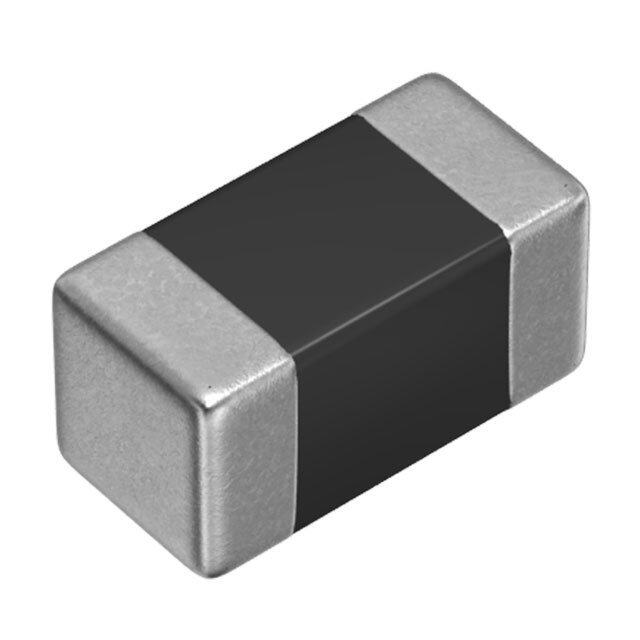
| 描述 | IC MULTIPLEXER DUAL SPDT 10TDFN |
| 产品分类 | |
| 品牌 | Intersil |
| 数据手册 | |
| 产品图片 |
|
| 产品型号 | ISL76120ARTZ |
| PCN组件/产地 | |
| rohs | 无铅 / 符合限制有害物质指令(RoHS)规范要求 |
| 产品系列 | - |
| 产品目录页面 | |
| 供应商器件封装 | 10-TDFN/MLP(3x3) |
| 功能 | 多路复用器 |
| 包装 | 管件 |
| 安装类型 | 表面贴装 |
| 导通电阻 | 10 欧姆 |
| 封装/外壳 | 10-VFDFN 裸露焊盘 |
| 工作温度 | -40°C ~ 105°C |
| 标准包装 | 100 |
| 电压-电源,单/双 (±) | 2.7 V ~ 5.5 V |
| 电压源 | 单电源 |
| 电流-电源 | 20nA |
| 电路 | 2 x SPDT |


- 商务部:美国ITC正式对集成电路等产品启动337调查
- 曝三星4nm工艺存在良率问题 高通将骁龙8 Gen1或转产台积电
- 太阳诱电将投资9.5亿元在常州建新厂生产MLCC 预计2023年完工
- 英特尔发布欧洲新工厂建设计划 深化IDM 2.0 战略
- 台积电先进制程称霸业界 有大客户加持明年业绩稳了
- 达到5530亿美元!SIA预计今年全球半导体销售额将创下新高
- 英特尔拟将自动驾驶子公司Mobileye上市 估值或超500亿美元
- 三星加码芯片和SET,合并消费电子和移动部门,撤换高东真等 CEO
- 三星电子宣布重大人事变动 还合并消费电子和移动部门
- 海关总署:前11个月进口集成电路产品价值2.52万亿元 增长14.8%


PDF Datasheet 数据手册内容提取
DATASHEET ISL76120 FN6711 Automotive Grade USB 2.0 High/Full Speed Multiplexer Rev 3.00 January 9, 2015 The Intersil ISL76120 dual 2:1 multiplexer IC is a single supply Features part that can operate from a single 2.7V to 5.5V supply. It contains two SPDT (Single Pole/Double Throw) switches • High speed (480Mbps) and full speed (12Mbps) signaling configured as a DPDT. The part was designed for switching capability per USB 2.0 between USB high-speed and USB full-speed sources in portable • 1.8V logic compatible (2.7V to +3.6V supply) battery powered products. • Enable pin to open all switches, simplifies multiple USB The normally-closed (NC) FSx switches can swing rail-to-rail and client management were specifically designed to pass USB full speed data signals • -3dB frequency (12Mbps) that range from 0V to 3.6V. The normally-open (NO) - HSx switches. . . . . . . . . . . . . . . . . . . . . . . . . . . . . . . . . . 880MHz HSx switches have high bandwidth and low capacitance and were specifically designed to pass USB high speed data signals - FSx switches. . . . . . . . . . . . . . . . . . . . . . . . . . . . . . . . . . 550MHz (480Mbps) with minimal distortion. • Crosstalk at 1MHz . . . . . . . . . . . . . . . . . . . . . . . . . . . . . . -70dB The part can be used in a variety of automotive entertainment • Off-isolation at 100kHz. . . . . . . . . . . . . . . . . . . . . . . . . . -98dB and infotainment applications where consumer USB devices • Single supply operation (VDD). . . . . . . . . . . . . . . . . 2.7V to 5.5V such as Portable Media Players (PMPs) are to be connected to embedded systems. The product allows switching between a • Available in TDFN package high-speed transceiver and a full-speed transceiver while • Robust ESD rating . . . . . . . . . . . . . . . . . . . . . . . . > 8.5kV HBM connected to a single USB host. Additionally, the part can be • Ultra-low operating current . . . . . . . . . . . . . . . . . . . . . . . 60nA used for charge control of PMPs. • -40°C to +105°C Operation The digital logic inputs are 1.8V logic compatible when operated with a 2.7V to 3.6V supply. The part has an enable pin to open • AEC-Q100 qualified component all switches. It can be used to facilitate proper bus disconnect • Pb-Free (RoHS Compliant) and connection when switching between the USB sources. Applications The ISL76120 is available in a 10 Ld 3mmx3mm TDFN package. It operates across a temperature range of -40°C to • Automotive +105°C. - USB docks - MP3 and PMP player attach kits - Infotainment systems • After market automotive options 3.3V µCONTROLLER VDD ISL76120 IN EN VBUS LOGIC CIRCUITRY R 4MΩ USB O HIGH-SPEED NECT D- HHSSDD12 TRANSCEIVER N COMD1 O C B D+ FSD1 USB S U COMD2 FULL-SPEED FSD2 TRANSCEIVER GND GND PORTABLE MEDIA DEVICE FIGURE 1. APPLICATION BLOCK DIAGRAM FN6711 Rev 3.00 Page 1 of 15 January 9, 2015
ISL76120 Pin Configuration ISL76120 (10 LD TDFN) TOP VIEW VDD 1 LOGIC 10 EN CONTROL 4M IN 2 9 HSD1 COMD1 3 8 HSD2 COMD2 4 7 FSD1 GND 5 6 FSD2 NOTE: 1. ISL76120 Switches Shown for IN = Logic “0” and EN = Logic “1”. Truth Table Pin Descriptions ISL76120 ISL76120 EN IN FSD1, FSD2 HSD1, HSD2 PIN NUMBER NAME FUNCTION 1 0 ON OFF 1 VDD Power Supply 1 1 OFF ON 2 IN Select Logic Control Input 0 X OFF OFF 3 COMD1 USB Common Port Logic “0” when 0.5V, Logic “1” when 1.4V with a 2.7V to 3.6V Supply. X = Don’t Care 4 COMD2 USB Common Port 5 GND Ground Connection 6 FSD2 Full Speed USB Differential Port 7 FSD1 Full Speed USB Differential Port 8 HSD2 High Speed USB Differential Port 9 HSD1 High Speed USB Differential Port 10 EN Bus Switch Enable Ordering Information PART NUMBER TEMP. RANGE PACKAGE (Notes2, 3, 4) PART MARKING (°C) (RoHS Compliant) PKG. DWG. # ISL76120ARTZ 6120 -40 to +105 10 Ld 3x3 TDFN L10.3x3A NOTES: 2. Add “-T*” suffix for tape and reel. Please refer to TB347 for details on reel specifications. 3. These Intersil Pb-free plastic packaged products employ special Pb-free material sets, molding compounds/die attach materials, and 100% matte tin plate plus anneal (e3 termination finish, which is RoHS compliant and compatible with both SnPb and Pb-free soldering operations). Intersil Pb-free products are MSL classified at Pb-free peak reflow temperatures that meet or exceed the Pb-free requirements of IPC/JEDEC J STD-020. 4. For Moisture Sensitivity Level (MSL), please see product information page for ISL76120. For more information on MSL, please see tech brief TB363. FN6711 Rev 3.00 Page 2 of 15 January 9, 2015
ISL76120 Absolute Maximum Ratings Thermal Information VDD to GND . . . . . . . . . . . . . . . . . . . . . . . . . . . . . . . . . . . . . . . . . -0.3V to 6.0V Thermal Resistance (Typical) JA (°C/W) JC (°C/W) Input Voltages 10 Ld 3x3 TDFN Package (Notes6, 7). . . . 50 9 FSD2, FSD1, HSD2, HSD1 (Note5) . . . . . . . . . . . . . - 1V to ((VDD) +0.3V) Maximum Junction Temperature (Plastic Package) . . . . . . . . . . . +150°C IN, EN (Note5) . . . . . . . . . . . . . . . . . . . . . . . . . . . . -0.3V to ((VDD) +0.3V) Maximum Storage Temperature Range. . . . . . . . . . . . . . . . . -65°C to +150°C Output Voltages Pb-Free Reflow Profile . . . . . . . . . . . . . . . . . . . . . . . . . . . . . . . . . . see TB493 COMD1, COMD2 (Note5) . . . . . . . . . . . . . . . . . . . . . . . . . . . . . . -1V to 5V Continuous Current (HSD2, HSD1, FSD2, FSD1) . . . . . . . . . . . . . . . ±40mA Operating Conditions Peak Current (HSD2, HSD1, FSD2, FSD1) (Pulsed 1ms, 10% Duty Cycle, Max). . . . . . . . . . . . . . . . . . . . . . ±100mA Temperature Range. . . . . . . . . . . . . . . . . . . . . . . . . . . . . . -40°C to +105°C VDD Supply Voltage Range . . . . . . . . . . . . . . . . . . . . . . . . . . . . 2.7V to 5.5V CAUTION: Do not operate at or near the maximum ratings listed for extended periods of time. Exposure to such conditions may adversely impact product reliability and result in failures not covered by warranty. NOTES: 5. Signals on FSD1, FSD2, HSD1, HSD2, COMD1, COMD2, EN, IN exceeding VDD or GND by specified amount are clamped. Limit current to maximum current ratings. 6. JA is measured in free air with the component mounted on a high effective thermal conductivity test board with “direct attach” features. See Tech Brief TB379. 7. For JC, the “case temp” location is the center of the exposed metal pad on the package underside. Electrical Specifications Test Conditions: VDD = +3.3V, GND = 0V, VINH = 1.4V, VINL = 0.5V, VENH = 1.4V, VENL = 0.5V, (Note8). Boldface limits apply across the operating temperature range, -40°C to +105°C. TEMP MIN MAX PARAMETER TEST CONDITIONS (°C) (Notes9, 10) TYP (Notes9, 10) UNITS ANALOG SWITCH CHARACTERISTICS NC Switches (FSD1, FSD2) Analog Signal Voltage Range, VANALOG VDD = 3.3V, IN = 0V, EN = 3.3V Full 0 - VDD V ON-Resistance, rON VDD = 3.3V, IN = 0.5V, EN = 1.4V, ICOMx = 40mA, +25 - 7 10 Ω VFSD1 or VFSD2 = 0V to 3.3V (see Figure5) Full - 7.8 15 Ω rON Matching Between Channels, rON VDD = 3.3V, IN = 0.5V, EN = 1.4V, ICOMx = 40mA, +25 - 0.1 1.2 Ω VFSD1 or VFSD2 = Voltage at max rON over signal range of 0V Full - 0.7 1.4 Ω to 3.3V (Note12) rON Flatness, rFLAT(ON) VDD = 3.3V, IN = 0.5V, EN = 1.4V, ICOMx = 40mA, +25 - 4 6 Ω VFSD1 or VFSD2 = 0V to 3.3V (Note11) Full - 4.1 8 Ω OFF Leakage Current, IFSX(OFF) V+ = 3.6V, IN = 3.6V, EN = 0V and 3.6V, VCOMx = 0.3V, 3V, +25 -20 0.4 20 nA VFSX = 3V, 0.3V Full -70 0.6 70 nA ON Leakage Current, IFSX(ON) V+ = 3.6V, IN = 0V, EN = 3.6V, VCOMx = 0.3V, 3V, +25 -20 2 20 nA VFSX = 0.3V, 3V Full -70 4.7 70 nA NO Switches (HSD1, HSD2) Analog Signal Voltage Range, VANALOG VDD = 3.3V, IN = 3.3V, EN = 3.3V Full 0 - VDD V ON-Resistance, rON VDD = 3.3V, IN = 1.4V, EN = 1.4V, ICOMx = 1mA, +25 - 25 30 Ω VHSD2 or VHSD1 = 3.3V (see Figure4) Full - 29 35 Ω ON-Resistance, rON VDD = 3.3V, IN = 1.4V, EN = 1.4V, ICOMx = 40mA, VHSD2 or +25 - 4.5 6 Ω VHSD1 = 0V to 400mV (see Figure4) Full - 5.1 9 Ω rON Matching Between Channels, rON VDD = 3.3V, IN = 1.4V, EN = 1.4V, ICOMx = 40mA, +25 - 0.2 1.3 Ω VHSD2 or VHSD1 = Voltage at max rON, Voltage at max rON Full - 0.7 1.5 Ω over signal range of 0V to 400mV (Note12) rON Flatness, rFLAT(ON) VDD = 3.3V, IN = 1.4V, EN = 1.4V, ICOMx = 40mA, VHSD2 or +25 - 0.4 1 Ω VHSD1 = 0V to 400mV (Note11) Full - 0.43 1.5 Ω FN6711 Rev 3.00 Page 3 of 15 January 9, 2015
ISL76120 Electrical Specifications Test Conditions: VDD = +3.3V, GND = 0V, VINH = 1.4V, VINL = 0.5V, VENH = 1.4V, VENL = 0.5V, (Note8). Boldface limits apply across the operating temperature range, -40°C to +105°C. (Continued) TEMP MIN MAX PARAMETER TEST CONDITIONS (°C) (Notes9, 10) TYP (Notes9, 10) UNITS OFF Leakage Current, IHSD2(OFF) or VDD = 3.6V, IN = 0V, EN = 0 and 3.6V, VCOMD1 or +25 -20 0.3 20 nA IHSD1(OFF) VCOMD2=3V, 0.3V, VHSD2 or VHSD1 = 0.3V, 3V Full -70 1 70 nA ON Leakage Current, IHSD2(ON) or VDD = 3.6V, IN = 3.6V, EN = 3.6V, VCOMD1 or +25 -20 4.8 20 nA IHSD1(ON) VCOMD2 = 0.3V, 3.0V, VHSD2 or VHSD1 = 0.3V, 3.0V Full -70 5 70 nA DYNAMIC CHARACTERISTICS Turn-ON Time, tON VDD = 3.3V, RL = 45Ω, CL = 10pF (see Figure2) +25 - 25 - ns Turn-OFF Time, tOFF VDD = 3.3V, RL = 45Ω, CL = 10pF (see Figure2) +25 - 15 - ns Break-Before-Make Time Delay, tD VDD = 3.3V, RL = 45Ω, CL = 10pF (see Figure3) +25 - 7 - ns Skew, tSKEW VDD = 3.3V, IN = 3.3V, EN = 3.3V, RL = 45Ω,CL = 10pF, +25 - 50 - ps (HSx Switch) tR=tF= 720ps at 480Mbps, (Duty Cycle = 50%) (see Figure8) Total Jitter, tJ VDD =3.3V, IN = 3.3V, EN = 3.3V, RL = 45Ω,CL = 10pF, +25 - 210 - ps (HSx Switch) tR=tF= 720ps at 480Mbps Propagation Delay, tPD VDD = 3.3V, IN = 3.3V, EN = 3.3V, RL = 45Ω,CL = 10pF +25 - 250 - ps (HSx Switch) seeFigure8) Skew, tSKEW VDD = 3.3V, IN = 0V, EN = 3.3V, RL = 39Ω,CL = 50pF, +25 - 0.15 - ns (FSx Switch) tR = tF = 12ns at 12Mbps, (Duty Cycle = 50%) (see Figure8) Rise/Fall Time Mismatch, tM VDD = 3.3V, IN = 0V, EN = 3.3V, RL = 39Ω,CL = 50pF, +25 - 10 - % (FSx Switch) tR = tF = 12ns at 12Mbps, (Duty Cycle = 50%) Total Jitter, tJ VDD = 3.3V, IN = 0V, EN = 3.3V, RL = 39Ω,CL = 50pF, +25 - 1.6 - ns (FSx Switch) tR = tF = 12ns at 12Mbps Propagation Delay, tPD VDD = 3.3V, IN = 0V, EN = 3.3V, RL = 39Ω,CL = 50pF +25 - 0.9 - ns (FSx Switch) seeFigure8) Crosstalk VDD = 3.3V, RL = 45Ω, f = 1MHz (see Figure7) +25 - -70 - dB Off Isolation VDD = 3.3V, RL = 45Ω, f = 100kHz +25 - -98 - dB FSx Switch -3dB Bandwidth Signal = -10dBm, 1.0VDC offset, RL = 45Ω,CL = 5pF +25 - 550 - MHz HSx Switch -3dB Bandwidth Signal = -10dBm, 0.2VDC offset, RL = 45Ω,CL = 5pF +25 - 880 - MHz HSx OFF Capacitance, CHSxOFF f = 1MHz, VDD = 3.3V, IN = 0V, EN = 3.3V, VHSD1 or +25 - 6 - pF VHSD2=VCOMx = 0V (see Figure6) FSx OFF Capacitance, CFSxOFF f = 1MHz, VDD = 3.3V, IN = 3.3V, EN = 3.3V, VFSD1 or +25 - 9 - pF VFSD2= VCOMx = 0V (see Figure6) COM ON Capacitance, CCOMX(ON) f = 1MHz, VDD = 3.3V, IN = 3.3V, EN = 3.3V, VHSD1 or +25 - 12 - pF VHSD2= VCOMx = 0V (see Figure6) COM ON Capacitance, CCOMX(ON) f = 1MHz, VDD = 3.3V, IN = 0V, EN = 3.3V, VFSD1 or +25 - 15 - pF VFSD2=VCOMx = 0V (see Figure6) POWER SUPPLY CHARACTERISTICS Power Supply Range, VDD Full 2.7 - 5.5 V Positive Supply Current, IDD VDD = 3.6V, IN = 0V or 3.6V, EN = 0V or 3.6V +25 - 20 60 nA Full - 114 250 nA FN6711 Rev 3.00 Page 4 of 15 January 9, 2015
ISL76120 Electrical Specifications Test Conditions: VDD = +3.3V, GND = 0V, VINH = 1.4V, VINL = 0.5V, VENH = 1.4V, VENL = 0.5V, (Note8). Boldface limits apply across the operating temperature range, -40°C to +105°C. (Continued) TEMP MIN MAX PARAMETER TEST CONDITIONS (°C) (Notes9, 10) TYP (Notes9, 10) UNITS DIGITAL INPUT CHARACTERISTICS Input Voltage Low, VINL, VENL VDD = 2.7V to 3.6V +25 - - 0.5 V Input Voltage High, VINH, VENH VDD = 2.7V to 3.6V +25 1.4 - - V Input Current, IINL, IENL VDD = 3.6V, IN = 0V, EN = 0V Full - 10 - nA Input Current, IINH VDD = 3.6V, IN = 3.6V Full - 10 - nA Input Current, IENH VDD = 3.6V, EN = 3.6V Full - 1 - µA NOTES: 8. VLOGIC = Input voltage to perform proper function. 9. The algebraic convention, whereby the most negative value is a minimum and the most positive a maximum, is used in this datasheet. 10. Parameters with MIN and/or MAX limits are 100% tested at +25°C, unless otherwise specified. Temperature limits established by characterization and are not production tested. 11. Flatness is defined as the difference between maximum and minimum value of on-resistance over the specified analog signal voltage range. 12. rON matching between channels is calculated by subtracting the channel with the highest max rON value from the channel with lowest max rON value, between HSD2 and HSD1 or between FSD2 and FSD1. Test Circuits and Waveforms VINH tr < 20ns VDD LOGIC 50% tf < 20ns INPUT VINL EN tOFF VINPUT HSx or FSx VOUT SWITCH INPUT COMx SWITCH INPUTVINPUT VOUT IN 90% 90% VIN GND RL CL SWITCH 45Ω 10pF OUTPUT 0V tON Logic input waveform is inverted for switches that have the opposite Repeat test for all switches. CL includes fixture and stray logic sense. capacitance. V = V ---------R-----L---------- OUT (INPUT) R +r L ON FIGURE 2A. MEASUREMENT POINTS FIGURE 2B. TEST CIRCUIT FIGURE 2. SWITCHING TIMES FN6711 Rev 3.00 Page 5 of 15 January 9, 2015
ISL76120 Test Circuits and Waveforms (Continued) VDD C VINH EN LOGIC INPUT FSD1 or FSD2 VINL VINPUT COMx VOUT HSD1 or HSD2 RL CL IN 45Ω 10pF SWITCH 90% OUTPUT VIN GND VOUT 0V tD Repeat test for all switches. CL includes fixture and stray capacitance. FIGURE 3A. MEASUREMENT POINTS FIGURE 3B. TEST CIRCUIT FIGURE 3. BREAK-BEFORE-MAKE TIME VDD VDD C C rON = V1/ICOMx rON = V1/40mA HSx FSx VHSX VFSX V1 IN 1.4V V1 IN 0.5V ICOMx COMx 40mA COMx GND EN GND EN 1.4V 1.4V Repeat test for all switches. Repeat test for all switches. FIGURE 4. HSx SWITCH rON TEST CIRCUIT FIGURE 5. FSx SWITCH rON TEST CIRCUIT FN6711 Rev 3.00 Page 6 of 15 January 9, 2015
ISL76120 Test Circuits and Waveforms (Continued) VDD VDD C C EN EN SIGNAL HSx OR FSx GENERATOR HSx COMx 45Ω IN IN IMPEDANCE ANALYZER VINL OR VIN VINH COMx GND COMx FSx ANALYZER NC GND RL Repeat test for all switches. Signal direction through switch is reversed, worst case values are recorded. Repeat test for all switches. FIGURE 6. CAPACITANCE TEST CIRCUIT FIGURE 7. CROSSTALK TEST CIRCUIT tri 90% 50% 10% DIN+ VDD tskew_i C DIN- 90% 50% 10% EN tfi VIN VIN tro 90% 15.8Ω COMD2 D2 OUT+ DIN+ OUT+ 10% 50% 143Ω CL 45Ω tskew_o 15.8Ω COMD1 D1 OUT- OUT- 50% DIN- 90% 143Ω CL 45Ω 10% tf0 GND |tro-tri| Change Due to Switch for Rising Input and Rising Output Signals. |tfo-tfi| Change Due to Switch for Falling Input and Falling Output Signals. |tskew_0| Skew through the Switch for Output Signals. |tskew_i| Skew through the Switch for Input Signals. FIGURE 8A. MEASUREMENT POINTS FIGURE 8B. TEST CIRCUIT FIGURE 8. SKEW TEST FN6711 Rev 3.00 Page 7 of 15 January 9, 2015
ISL76120 Application Block Diagram 3.3V µCONTROLLER VDD ISL76120 IN EN VBUS LOGIC CIRCUITRY 4MΩ USB OR HIGH-SPEED T HSD1 C D- TRANSCEIVER E HSD2 N COMD1 N O C B D+ FSD1 USB S U FULL-SPEED COMD2 FSD2 TRANSCEIVER GND GND PORTABLE MEDIA DEVICE FN6711 Rev 3.00 Page 8 of 15 January 9, 2015
ISL76120 Detailed Description The HSx switches can also pass USB full-speed signals (12Mbps) with minimal distortion and meet all the USB requirements for The ISL76120 device is a dual single pole/double throw (SPDT) USB 2.0 full-speed signaling (see Figure12). analog switch that operates from a single DC power supply in the The maximum signal range for the HSx switches is from -1V to range of 2.7V to 5.5V. It was designed to function as a dual 2-to-1 multiplexer to select between a USB high-speed transceiver and VDD. The signal voltage should not be allow to exceed the VDD voltage rail or go below ground by more than -1V. a USB full-speed transceiver in automotive applications. It is offered in a TDFN package for use in automotive Portable Media The HSx switches are active (turned ON) whenever the IN voltage Player docking stations and Apple iPod type players. The device is ≥1.4V and the EN logic voltage is ≥1.4V when operated with a has an enable pin to open all switches. 2.7V to 3.6V supply. The part consists of two full speed (FSx) switches and two ISL76120 Operation high-speed (HSx) switches. The FSx switches can swing from 0V to VDD. They were designed to pass USB full-speed (12Mbps) The discussion that follows will discuss using the ISL76120 in the differential data signals with minimal distortion. The HSx “Application Block Diagram” on page8. switches have high bandwidth and low capacitance to pass USB POWER high-speed (480Mbps) differential data signals with minimal edge and phase distortion. The power supply connected at the VDD (pin 1) provides the DC bias voltage required by the ISL76120 part for proper operation. The ISL76120 was designed for automotive USB applications The ISL76120 can be operated with a VDD voltage in the range of such as docking stations for Portable Media Players and other 2.7V to 5.5V. When used in a USB application, the VDD voltage general purpose USB connections that have both high-speed and should be kept in the range of 3.0V to 5.5V to ensure you get the full-speed transceivers and need to multiplex between these USB proper signal levels for good signal quality. sources to a single USB host (computer). This functionality is shown in the “Application Block Diagram” on page8. A 0.01µF or 0.1µF decoupling capacitor should be connected from the VDD pin to ground to filter out any power supply noise A detailed description of the two types of switches are provided from entering the part. The capacitor should be located as close in the following sections. to the VDD pin as possible. FSx Switches (FSD1, FSD2) LOGIC CONTROL The two FSx switches (FSD1, FSD2) are bidirectional switches The state of the ISL76120 device is determined by the voltage at that can pass rail-to-rail signals. They were specifically designed the IN pin (pin 2) and the EN pin (pin 10). IN is only active when to pass USB full-speed (12Mbps) differential signals and meet the EN pin is logic “1” (High). Refer to the “Truth Table” on page2. the USB 2.0 full-speed signal quality specifications see Figure9. The EN pin is internally pulled low through a 4MΩresistor to The FSx switches can also pass USB high speed signals ground. For logic “0” (Low) it can be driven low or allowed to (480Mbps) but do not quite meet the USB 2.0 high speed signal Float. The IN pin must be driven low or high and cannot be left quality eye diagram compliance requirement. floating. The maximum signal range for the FSx switches is from -1V to Logic Control Voltage Levels VDD. The signal voltage should not be allowed to exceed the VDD voltage rail or go below ground by more than -1V. EN = Logic “0” (Low) when VEN ≤0.5V or Floating. EN = Logic “1” (High) when VEN ≥1.4V When operated with a 2.7V to 3.6V supply, the FSx switches are IN = Logic “0” (Low) when VIN ≤0.5V. active (turned ON) whenever the IN logic control voltage is ≤0.5V IN = Logic “1” (High) when VIN ≥1.4V and the EN logic voltage ≥1.4V. HSx Switches (HSD1, HSD2) The two HSx switches (HSD2, HSD1) are bidirectional switches that can pass rail-to-rail signals. The ON-resistance is low and well matched between the HSD1 and HSD2 switches over the USB high-speed signal range, ensuring minimal impact by the switches to USB high-speed signal transitions. As the signal level increases, the rON switch resistance increases. The HSx switches were specifically designed to pass USB 2.0 high-speed (480Mbps) differential signals typically in the range of 0V to 400mV. They have low capacitance and high bandwidth to pass the USB high-speed signals with minimum edge and phase distortion to meet USB 2.0 high-speed signal quality specifications (see Figures10 and 11). FN6711 Rev 3.00 Page 9 of 15 January 9, 2015
ISL76120 Full-speed Mode If the IN pin = Logic “0” and the EN pin = Logic “1”, the part will be in the full-speed mode. In this mode, the FSD1 and FSD2 switches are ON and the HSD1 and HSD2 switches are OFF (high impedance). In a typical application, VDD will be in the range of 2.8V to 3.6V and will be connected to the battery or LDO of the portable media device. When a computer or USB hub is plugged into the common USB connector and the part is in the full-speed mode, a link will be established between the full-speed driver section of the media player and the computer. The device will be able to transmit and receive data from the computer at a data rate of 12Mbps. High-speed Mode If the IN pin = Logic “1” and the EN pin = Logic “1”, the part will go into high-speed mode. In high-speed mode, the HSD1 and HSD2 switches are ON and the FSD1 and FSD2 switches are OFF (high impedance). When a USB cable from a computer or USB hub is connected at the common USB connector and the part is in the high-speed mode, a link will be established between the high-speed driver section of the media player and the computer. The device will be able to transmit and receive data from the computer at a data rate of 480Mbps. All Switches OFF Mode If the IN pin = Logic “0” or Logic “1” and the EN pin = Logic “0”, all of the switches will turn OFF (high impedance). The all OFF state can be used to switch between the two USB sections of the media player. When disconnecting from one USB device to the other USB device, you can momentarily put the ISL76120 switch in the “all off” state in order to get the computer to disconnect from the one device so it can properly connect to the other USB device when that channel is turned ON. FN6711 Rev 3.00 Page 10 of 15 January 9, 2015
ISL76120 Typical Performance Curves TA = +25°C, Unless Otherwise Specified. VDD = 3.3V FIGURE 9. EYE PATTERN: 12MBPS USB SIGNAL WITH FSx SWITCHES IN THE SIGNAL PATH VDD = 3.3V FIGURE 10. EYE PATTERN WITH FAR END MASK: 480MBPS USB SIGNAL WITH HSx SWITCHES IN THE SIGNAL PATH FN6711 Rev 3.00 Page 11 of 15 January 9, 2015
ISL76120 Typical Performance Curves TA = +25°C, Unless Otherwise Specified. (Continued) VDD = 3.3V FIGURE 11. EYE PATTERN WITH NEAR END MASK: 480MBPS USB SIGNAL WITH HSx SWITCHES IN THE SIGNAL PATH VDD = 3.3V FIGURE 12. EYE PATTERN: 12MBPS USB SIGNAL WITH HSx SWITCHES IN THE SIGNAL PATH FN6711 Rev 3.00 Page 12 of 15 January 9, 2015
ISL76120 Typical Performance Curves TA = +25°C, Unless Otherwise Specified. (Continued) 5.5 -10 RL = 45Ω +105°C -20 VIN = 0.2VP-P TO 2VP-P 5.0 -30 +85°C B) -40 4.5 N (d AI -50 ()N4.0 +25°C ED G -60 O Z r ALI -70 M 3.5 R O -80 N -40°C -90 3.0 -110 2.5 0 0.1 0.2 0.3 0.4 0.001M 0.01M 0.1M 1M 10M 100M 500M VCOM (V) FREQUENCY (Hz) FIGURE 13. HSx SWITCH ON-RESISTANCE vs SWITCH VOLTAGE FIGURE 14. OFF-ISOLATION -10 RL = 45Ω -20 VIN = 0.2VP-P TO 2VP-P -30 dB) -40 N ( AI -50 G D E -60 Z LI A -70 M R O -80 N -90 -110 0.001M 0.01M 0.1M 1M 10M 100M 500M FREQUENCY (Hz) FIGURE 15. CROSSTALK Die Characteristics SUBSTRATE POTENTIAL (POWERED UP): GND (TDFN Paddle Connection: Tie to GND or Float) TRANSISTOR COUNT: 98 PROCESS: Submicron CMOS FN6711 Rev 3.00 Page 13 of 15 January 9, 2015
ISL76120 Revision History The revision history provided is for informational purposes only and is believed to be accurate, but not warranted. Please go to the web to make sure that you have the latest revision. DATE REVISION CHANGE January 9, 2015 FN6711.3 Converted to new template and implemented Intersil Standards. Added Revision History. In “Thermal Information” on page3 changed theta JA from 55°C/W to 50°C/W. Added theta JC of 9°C/W. Revised Note6 with new statement: Theta-JA is measured in free air with the component mounted on a high effective thermal conductivity test board with “direct attach” features. See Tech Brief TB379. Added Note7: For theta-JC, the "case temperature" location is the center of the exposed metal pad on the package underside. Updated POD L10.3x3A with following changes: Added Typical Recommended Land Pattern Converted to new format by moving dimensions from table onto drawing (no dimension changes). About Intersil Intersil Corporation is a leading provider of innovative power management and precision analog solutions. The company's products address some of the largest markets within the industrial and infrastructure, mobile computing and high-end consumer markets. For the most updated datasheet, application notes, related documentation and related parts, please see the respective product information page found at www.intersil.com. You may report errors or suggestions for improving this datasheet by visiting www.intersil.com/ask. Reliability reports are also available from our website at www.intersil.com/support © Copyright Intersil Americas LLC 2008-2015. All Rights Reserved. All trademarks and registered trademarks are the property of their respective owners. For additional products, see www.intersil.com/en/products.html Intersil Automotive Qualified products are manufactured, assembled and tested utilizing TS16949 quality systems as noted in the quality certifications found at www.intersil.com/en/support/qualandreliability.html Intersil products are sold by description only. Intersil may modify the circuit design and/or specifications of products at any time without notice, provided that such modification does not, in Intersil's sole judgment, affect the form, fit or function of the product. Accordingly, the reader is cautioned to verify that datasheets are current before placing orders. Information furnished by Intersil is believed to be accurate and reliable. However, no responsibility is assumed by Intersil or its subsidiaries for its use; nor for any infringements of patents or other rights of third parties which may result from its use. No license is granted by implication or otherwise under any patent or patent rights of Intersil or its subsidiaries. For information regarding Intersil Corporation and its products, see www.intersil.com FN6711 Rev 3.00 Page 14 of 15 January 9, 2015
ISL76120 Package Outline Drawing L10.3x3A 10 LEAD THIN DUAL FLAT NO-LEAD PLASTIC PACKAGE Rev 5, 3/10 2.0 REF 3.00 A 6 PIN 1 8X 0.50 BSC INDEX AREA B 1 5 6 PIN 1 10X 0 . 30 INDEX AREA 3.00 1.50 0.15 (4X) 0.10 M C A B 10 5 0.05 M C 4 10 X 0.25 TOP VIEW 2.30 ( 2.30 ) BOTTOM VIEW 0 .80 MAX SEE DETAIL "X" 0.10C C (2.90) SEATING PLANE (1.50) 0.08 C SIDE VIEW (10 X 0.50) 5 0 . 2 REF ( 8X 0 .50 ) C ( 10X 0.25 ) 0 . 00 MIN. 0 . 05 MAX. TYPICAL RECOMMENDED LAND PATTERN DETAIL "X" NOTES: 1. Dimensions are in millimeters. Dimensions in ( ) for Reference Only. 2. Dimensioning and tolerancing conform to ASME Y14.5m-1994. 3. Unless otherwise specified, tolerance : Decimal ± 0.05 Angular ±2.50° 4. Dimension applies to the metallized terminal and is measured between 0.15mm and 0.30mm from the terminal tip. 5. Tiebar shown (if present) is a non-functional feature. 6. The configuration of the pin #1 identifier is optional, but must be located within the zone indicated. The pin #1 identifier may be either a mold or mark feature. 7. Compliant to JEDEC MO-229-WEED-3 except exposed pad length (2.30mm). FN6711 Rev 3.00 Page 15 of 15 January 9, 2015