ICGOO在线商城 > ISL6423BERZ
 Datasheet下载
- 型号: ISL6423BERZ
- 制造商: Intersil
- 库位|库存: xxxx|xxxx
- 要求:
| 数量阶梯 | 香港交货 | 国内含税 |
| +xxxx | $xxxx | ¥xxxx |
查看当月历史价格
查看今年历史价格
ISL6423BERZ产品简介:
ICGOO电子元器件商城为您提供ISL6423BERZ由Intersil设计生产,在icgoo商城现货销售,并且可以通过原厂、代理商等渠道进行代购。 提供ISL6423BERZ价格参考以及IntersilISL6423BERZ封装/规格参数等产品信息。 你可以下载ISL6423BERZ参考资料、Datasheet数据手册功能说明书, 资料中有ISL6423BERZ详细功能的应用电路图电压和使用方法及教程。
ISL6423BERZ 是瑞萨电子(Renesas Electronics America Inc.)推出的专用电源管理IC(PMIC),属于“稳压器—特殊用途”类别。其核心应用场景为单芯片双路输出卫星调谐器(Satellite Tuner)供电方案,广泛用于数字卫星接收设备(如DVB-S/S2机顶盒、卫星电视调谐模块、高清卫星接收卡等)。

该器件集成了两路高性能DC-DC稳压器:一路为可调输出(0.6V–3.3V,最大1.5A),专为给射频(RF)前端的低噪声放大器(LNA)和混频器供电;另一路为固定3.3V输出(最大300mA),用于为数字解调芯片或微控制器供电。它支持I²C接口配置,具备精确的电压调节、快速瞬态响应、过流/过温保护,并内置LNB(Low-Noise Block downconverter)供电所需的22kHz音调信号发生器和13/18V极化电压切换功能——这使其成为符合EN 50494/EN 50607标准的单线缆(Unicable™/JESS)卫星系统的关键电源芯片。

典型应用还包括便携式卫星通信终端、车载卫星导航接收模块及专业级卫星信号分析设备中的紧凑型、高集成度电源设计。其高效率(>90%)、小尺寸QFN封装(5×5mm)及低EMI特性,特别适合空间受限且对供电精度与可靠性要求严苛的射频系统。
| 参数 | 数值 |
| 产品目录 | 集成电路 (IC) |
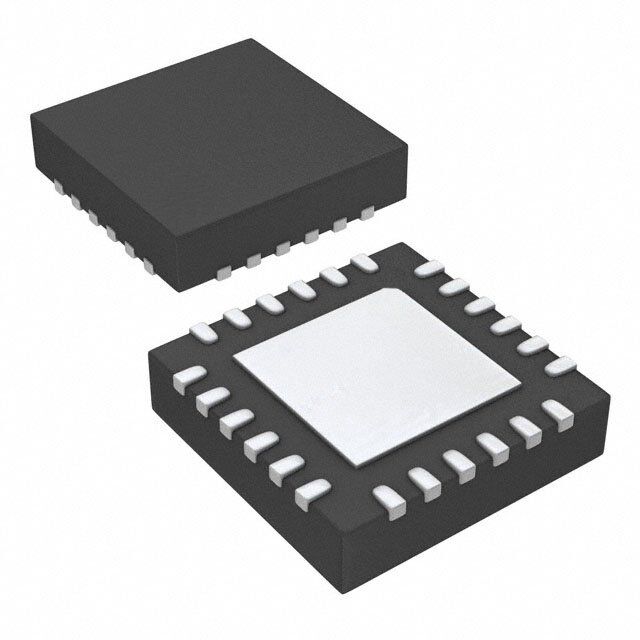
| 描述 | IC VREG SGL LNB W/I2C 24-QFN |
| 产品分类 | |
| 品牌 | Intersil |
| 数据手册 | |
| 产品图片 |
|
| 产品型号 | ISL6423BERZ |
| PCN设计/规格 | |
| rohs | 无铅 / 符合限制有害物质指令(RoHS)规范要求 |
| 产品系列 | - |
| 供应商器件封装 | 24-QFN-EP (4x4) |
| 包装 | 管件 |
| 安装类型 | 表面贴装 |
| 封装/外壳 | 24-VFQFN 裸露焊盘 |
| 工作温度 | -20°C ~ 85°C |
| 应用 | 转换器,卫星信号接收机顶盒设计 |
| 标准包装 | 75 |
| 电压-输入 | 8 V ~ 14 V |
| 电压-输出 | 13.3 V ~ 18.3 V,14.3 V ~ 19.3 V |
| 输出数 | 1 |


- 商务部:美国ITC正式对集成电路等产品启动337调查
- 曝三星4nm工艺存在良率问题 高通将骁龙8 Gen1或转产台积电
- 太阳诱电将投资9.5亿元在常州建新厂生产MLCC 预计2023年完工
- 英特尔发布欧洲新工厂建设计划 深化IDM 2.0 战略
- 台积电先进制程称霸业界 有大客户加持明年业绩稳了
- 达到5530亿美元!SIA预计今年全球半导体销售额将创下新高
- 英特尔拟将自动驾驶子公司Mobileye上市 估值或超500亿美元
- 三星加码芯片和SET,合并消费电子和移动部门,撤换高东真等 CEO
- 三星电子宣布重大人事变动 还合并消费电子和移动部门
- 海关总署:前11个月进口集成电路产品价值2.52万亿元 增长14.8%

PDF Datasheet 数据手册内容提取
DATASHEET ISL6423B FN6412 Single Output LNB Supply and Control Voltage Regulator with I2C Interface for Rev 1.00 Advanced Satellite Set-Top Box Designs Apr 10, 2007 The ISL6423B is a highly integrated voltage regulator and Features interface IC, specifically designed for supplying power and • Single Chip Power solution control signals from advanced satellite set-top box (STB) - Operation for 1-Tuner/1-Dish Applications modules to the low noise blocks (LNBs) of singe antenna - Integrated DC/DC Converter and I2C Interface ports. The device consists of a current-mode boost PWM and a low-noise linear regulator along with the circuitry • Switch-Mode Power Converter for Lowest Dissipation required for 22kHz tone generation, modulation and I2C - Boost PWMs with >92% Efficiency device interface. The device makes the total LNB supply - Selectable 13.3V or 18.3V Outputs design simple, efficient and compact with low external - Digital Cable Length Compensation (1V) component count. - I2C and Pin Controllable Output The current-mode boost converters provides the linear • Output Back Bias Capability of 28V regulator with input voltage that is set to the final output • I2C Compatible Interface for Remote Device Control voltages, plus typically 0.8V to insure minimum power dissipation across each linear regulator. This maintains • Registered Slave Address 0001 00XX constant voltage drop across the linear pass element while • 2.5V, 3.3V, 5V Logic Compatible permitting adequate voltage range for tone injection. • External Pin to Toggle Between V and H Polarization The final regulated output voltage is available at output • Built-In Tone Oscillator Factory Trimmed to 22kHz terminals to support the operation of an antenna port for - Facilitates DiSEqC (EUTELSAT) Encoding single tuners. The outputs for each PWM can be controlled in two ways, full control from I2C using the VTOP and VBOT - External Modulation Input bits or set the I2C to the lower range i.e., 13V/14V, and • Internal Over-Temperature Protection and Diagnostics switch to higher range i.e., 18V/19V, with the SELVTOP pin. • Internal OV, UV, Overload and Overtemp Flags All the functions on this IC are controlled via the I2C bus by (Visible on I2C) writing 8 bits words onto the System Registers (SR). The same register can be read back, and five I2C bits will report • FLT signal the diagnostic status. Separate enable command sent on the • LNB Short-Circuit Protection and Diagnostics I2C bus provides for standby mode control for the PWM and • QFN, EPTSSOP Packages linear combination, disabling the output and forcing a shutdown mode. The output channel is capable of providing 750mA of • Pb-Free Available (RoHS Compliant) continuous current. The overcurrent limit can be digitally Applications programmed to four levels. The External modulation input EXTM can accept a • LNB Power Supply and Control for Satellite Set-Top Box modulated Diseqc command and transfer it symmetrically to Ordering Information the output. Alternatively the EXTM pin can be used to modulate the continuos internal tone. PART PART TEMP. PKG. NUMBER* MARKING (°C) PACKAGE DWG. # The FLT pin serves as an interrupt for the processor when ISL6423BERZ 6423BERZ -20 to +85 24 Ld 4x4 QFN L24.4x4D any condition turns OFF the LNB controller (Over (Note) (Pb-free) Temperature, Overcurrent, Disabled). The nature of the Disable can be read of the I2C registers. ISL6423BEVEZ ISL6423BEVEZ -20 to +85 28 Ld EPTSSOPM28.173B (Note) (Pb-free) NOTE: Intersil Pb-free plus anneal products employ special Pb-free material sets; molding compounds/die attach materials and 100% matte tin plate termination finish, which are RoHS compliant and compatible with both SnPb and Pb-free soldering operations. Intersil Pb-free products are MSL classified at Pb-free peak reflow temperatures that meet or exceed the Pb-free requirements of IPC/JEDEC J STD-020. Add “-T” suffix for tape and reel. FN6412 Rev 1.00 Page 1 of 16 Apr 10, 2007
ISL6423B Pinouts ISL6423B (28 LD EPTSSOP) TOP VIEW VCC 1 28 CPSWIN NC 2 27 CPSWOUT FLT 3 26 CPVOUT SGND 4 25 EXTM SGND 5 24 SDA TCAP 6 23 SCL ADDR0 7 22 TDOUT ADDR1 8 21 TDIN BYPASS 9 20 VO PGND 10 19 NC GATE 11 18 NC VSW 12 17 AGND NC 13 16 SELVTOP CS 14 15 TXT ISL6423B (24 LD QFN) TOP VIEW T D WIN WOU OUT GN LT CC PS PS PV S F V C C C 24 23 22 21 20 19 SGND 1 18 EXTM TCAP 2 17 SDA ADDR0 3 16 SCL ADDR1 4 15 TDOUT BYPASS 5 14 TDIN PGND 6 13 VO 7 8 9 10 11 12 ATE SW S XT VTOP GND G V C T L A E S FN6412 Rev 1.00 Page 2 of 16 Apr 10, 2007
ApFN Block Diagram IS r 10, 206412R 11 17 16 3 4 23 L6423B 0e OLF/BCF 7v 1.00 COUNTER LOOPVGREIOCRT CSEUCCRHTREIOEMNNET 1 DCL VTOP SDA SCL ADDR0 ADDR1 FLT PWM OC1 SEL UVF LOGIC O GATE 7 Q CLK1 S SDA SCL ADDR0 OUVF ADDR1 6 PGND ISELL&H OLF/BCF OTF STHHUETRDMOAWLN EN I2C ENT INTERFACE TTH CS ILIM1 +- DCL AMP VTOP VBOT CS 9 SLOPE CLK1 OSC. COMPENSATION BAND GAP REF VOLTAGE TDOUT BGV 15 DIV & WAVE SHAPING TXT -+ TONE REF DECODER VOLTAGE TDIN TTH VREF1 ADJ1 INT 14 TONE TONE INJ CKT VSW 8 1 L E 13 VO MS + - AGND 12 EXT TONE CKT VCC 22 ON CHIP LINEAR SGND 1 UVLO SGND POR ENT1 24 SOFT-START T Page BYPASS ESINONT1F 5/TEV-NS2TART TXT TCAP EXTM CPSWOU CPSWIN CHARGE CPPUVMOPUT 3 o f 16 NOTE: 5 10 2 18 20 21 19 1. Pinouts shown are for the QFN package.
ApFN Typical Application Schematic QFN IS r 10, 206412R L6423B 0e VIN 7v 1 .0 RTN 0 0 FLT BAR EXTM C29 R11 100 1n SDA C24 C2547n R12 100 1µF 0 SCL L4 220µH 1 2 0 432109 222221 C15 0.22µF DTCNTT D6 C27 0.22µF 12 SGND SGNFLVCCPSWICPSWOUCPVOU EXTM 1187 C0.218µFCMS06 R1023k R7 15 VLNB TCAP SDA 3 16 M6 ADDR0 U2 SCL 4 15 NDS356AP C562µ3F R1180 0 C26 1µF 56 ABPGDYPNDARDS1SISL6423OPER TDTODVUIONT 1143 R4.274k D1.85KE24 0 123 0 7GATE8VSW9CS10TXT11SELVT12AGND C101n6 R13R4.272k Q2N42222A RTN 2 TPC6002 47k Q2 R9 470 L5 TXT 15µH R8 C21 TDOUT 1 654 0.1 100pF SELVTOP D7 CMS06 0 0 D5 L6 4.7µH 1 2 NOTE : SDA and SCL require pull up to the required logic level. CMS06 C22 C18 C19 C20 56µF 10µF 10µF 10µF P a g 0 0 0 0 e 4 o f 1 6
ISL6423B Absolute Maximum Ratings Thermal Information Supply Voltage, VCC . . . . . . . . . . . . . . . . . . . . . . . . . .8.0V to 18.0V Thermal Resistance (Typical, Notes 2, 3) JA (°C/W) JC (°C/W) Logic Input Voltage Range QFN Package (Notes 2, 3). . . . . . . . . . 38 4.5 (SDA, SCL, ENT, DSQIN 1 and 2, SEL18V 1 and 2). -0.5V to 7V EPTSSOP Package (Notes 2, 3) . . . . . 35 2.5 Maximum Junction Temperature (Note 4) . . . . . . . . . . . . . . .+150°C Maximum Storage Temperature Range. . . . . . . . . .-40°C to +150°C Operating Temperature Range . . . . . . . . . . . . . . . . .-20°C to +85°C CAUTION: Stresses above those listed in “Absolute Maximum Ratings” may cause permanent damage to the device. This is a stress only rating and operation of the device at these or any other conditions above those indicated in the operational sections of this specification is not implied. NOTES: 2. JA is measured in free air with the component mounted on a high effective thermal conductivity test board with “direct attach” features. See Tech Brief TB379. 3. For JC, the "case temp" location is the center of the exposed metal pad on the package underside. 4. +150°C max junction temperature is intended for short periods of time to prevent shortening the lifetime. Operation close to +150°C junction may trigger the shutdown of the device even before +150°C, since this number is specified as typical. Electrical Specifications VCC = 12V, TA = -20°C to +85°C, unless otherwise noted. Typical values are at TA = +25°C. EN = H, VTOP VBOT = L, ENT = L, DCL = L, IOUT = 12mA, unless otherwise noted. See software description section for I2C access to the system. PARAMETER SYMBOL TEST CONDITIONS MIN TYP MAX UNITS Operating Supply Voltage Range 8 12 14 V Standby Supply Current EN = L - 1.5 3.0 mA Supply Current IIN EN = VTOP = VBOT = ENT = H, No Load - 4.0 8.0 mA UNDERVOLTAGE LOCKOUT Start Threshold 7.5 - 7.95 V Stop Threshold 7.0 - 7.55 V Start to Stop Hysteresis 350 400 500 mV SOFT-START COMP Rise Time (Note 5) (Note 5) - 8196 - Cycles Output Voltage (Note 5) VO1 (Refer to Table 1) 13.04 13.3 13.56 V VO1 (Refer to Table 1) 14.02 14.3 14.58 V VO1 (Refer to Table 1) 17.94 18.3 18.66 V VO1 (Refer to Table 1) 19.00 19.3 19.68 V Line Regulation DVO1, VIN = 8V to 14V; VO = 13.3V - 4.0 40.0 mV DVO2 VIN = 8V to 14V; VO = 18.3V - 4.0 60.0 mV Load Regulation DVO1, IO = 0mA to 350mA - 50 80 mV DVO2 IO = 0mA to 750mA - 100 200 mV Dynamic Output Current Limiting IMAX DCL = 0, ISEL H = 0, ISEL L = 0 (Note 8) 275 305 345 mA DCL = 0, ISEL H = 0, ISEL L = 1 (Note 8) 515 570 630 mA DCL = 0, ISEL H = 1, ISEL L = 0 (Note 8) 635 705 775 mA DCL = 0, ISEL H = 1, ISEL L = 1 (Note 8) 800 890 980 mA Dynamic Overload Protection Off Time TOFF DCL = 0, Output Shorted (Note 8) - 900 - ms Dynamic Overload Protection On Time TON - 51 - ms Static Output Current Limiting IMAX DCL = 1 (Note 8) - 1000 - mA Cable Fault CABF Threshold ICAB EN = 1, VO = 19V, No Tone. 2 10 20 mA FN6412 Rev 1.00 Page 5 of 16 Apr 10, 2007
ISL6423B Electrical Specifications VCC = 12V, TA = -20°C to +85°C, unless otherwise noted. Typical values are at TA = +25°C. EN = H, VTOP VBOT = L, ENT = L, DCL = L, IOUT = 12mA, unless otherwise noted. See software description section for I2C access to the system. (Continued) PARAMETER SYMBOL TEST CONDITIONS MIN TYP MAX UNITS TONE OSCILLATOR Tone Frequency ftone ENT = H 20.0 22.0 24.0 kHz Tone Amplitude Vtone ENT = H, IO = 5mA 500 680 800 mV Tone Duty Cycle dctone ENT = H, 40 50 60 % Tone Rise or Fall Time Tr, Tf ENT = H, 5 10 14 s TONE DECODER Input Amplitude Vtdin 200 - 1000 mV Frequency Capture Range Ftdin 17.5 - 26.5 kHz Input Impedance Zdet - 8.6 - k Detector Output Voltage Vtdout_L Tone Present, ILOAD = 3mA - - 0.4 V Detector Output Leakage Itdout_H Tone absent, VO = 6V - - 10 A Tone Decoder Rx Threshold VRXth TXT = L and TTH = 0 (Note 9) 100 150 200 mV Tone Decoder Tx Threshold VTXth TXT = H and TTH = 0 (Note 9) 400 450 500 mV LINEAR REGULATOR Drop-out Voltage IOUT = 750mA - 0.8 1.05 V Output Backward Leakage Current IBKLK EN = 0; VOBK = 27V - 2.0 3.0 mA Output Backward Leakage Current IBKLK EN = 0; VOBK = 28V - 3.0 17 mA Output Backward Current Threshold IBKTH EN = 1; VOFAULT = 19V (Note 7) - 140 - mA Output Backward Current Limit IBKLM EN = 1; VOFAULT = 19V (Note 7) - 350 - mA Output Backward Voltage VOBK EN = 0 - - 27 V Output Under Voltage OUVF bit is asserted high, Measured from -6 - -2 % (Asserted high during soft-start) the typ. output set value Output Over Voltage OUVF bit is asserted high, Measured from +2 - +6 % (Asserted high during soft-start) the typ. output set value TXT, EXTM, SELVTOP AND ADDR 0/1 INPUT PINs (Note 8) Asserted LOW - - 0.8 V Asserted HIGH 1.7 - - V Input Current - 25 - A CURRENT SENSE (CS pin) Input Bias Current IBIAS - 700 - nA Overcurrent Threshold VCS Static current mode, DCL = H 325 450 500 mV ERROR AMPLIFIER Open Loop Voltage Gain AOL - 93 - dB Gain Bandwidth Product GBP - 14 - MHz PWM Maximum Duty Cycle 90 93 - % Minimum Pulse Width - 20 - ns FN6412 Rev 1.00 Page 6 of 16 Apr 10, 2007
ISL6423B Electrical Specifications VCC = 12V, TA = -20°C to +85°C, unless otherwise noted. Typical values are at TA = +25°C. EN = H, VTOP VBOT = L, ENT = L, DCL = L, IOUT = 12mA, unless otherwise noted. See software description section for I2C access to the system. (Continued) PARAMETER SYMBOL TEST CONDITIONS MIN TYP MAX UNITS OSCILLATOR Oscillator Frequency fo Fixed at (20)(ftone) 396 440 484 kHz Thermal Shutdown Temperature Shutdown Threshold - 150 - °C Temperature Shutdown Hysteresis - 20 - °C OTFI FLT (released) VO = 6V - - 10 A FLT (asserted) ISINK = 3.2mA - - 0.4 V NOTES: 5. Internal digital soft-start 6. EXTM, TXT and SELVTOP and addr 0/1 pins have 200k internal pulldown resistors. 7. On exceeding this backward current limit threshold for a period of 2ms, the device enters the Backward dynamic current limit mode (350mA typ) and the BCF I2C bit is set. The dynamic current limit duty ratio during a back current fault is ON = 2ms/OFF = 50ms. The output will remain clamped to the fault output voltage till released. On removal of the fault condition the device returns to normal operation 8. In the Dynamic current limit mode the output is ON for 51ms and OFF for 900ms. But remains continuously ON in the Static mode. When tone is ON the minimum current limit is 50mA lower the values indicated in the table. Tone Waveform ENT I2C MSEL I2C EXTM PIN VOUT PIN 22kHz 22kHz 22kHz 22kHz 22kHz 22kHz INTERNAL TONE INTERNAL TONE EXTERNAL TONE RETURNS TO NOMINAL VOUT ~1 PERIOD Tr = 10µs TYP Tr = 10µs TYP AFTER THE LAST EXTM RISING EDGE T > 55µs; NOTES: 9. The signal pin TXT changes the decoder threshold during tone transmit and receive. TTH allows threshold control through I2C. 10. The tone rise and fall times are not shown due to resolution of graphics. It is 10µs typ for 22kHz. 11. The EXTM pins have input thresholds of Vil(max) = 0.8V and Vih(min) = 1.7V FIGURE 1. TONE WAVEFORM FN6412 Rev 1.00 Page 7 of 16 Apr 10, 2007
ISL6423B Typical Performance Curves 0.80 0.80 0.70 0.70 0.60 0.60 IOUT_max IOUT_max 0.50 0.50 A) A) (UT 0.40 (UT 0.40 O O I 0.30 I 0.30 0.20 0.20 0.10 0.10 0.00 0.00 0 20 40 60 80 0 20 40 60 80 TEMPERATURE (°C) TEMPERATURE (°C) FIGURE 2. OUTPUT CURRENT DERATING (EPTSSOP) FIGURE 3. OUTPUT CURRENT DERATING (4x4 QFN) Functional Pin Description SYMBOL FUNCTION SDA Bidirectional data from/to I2C bus. SCL Clock from I2C bus. VSW Input of the linear post-regulator. PGND Dedicated ground for the output gate driver of respective PWM. CS Current sense input; connect the sense resistor Rsc at this pin for desired peak overcurrent value for the boost FET. The set peak limit is effective in the static mode current limit only i.e., DCL = HIGH. SGND Small signal ground for the IC. TCAP Capacitor for setting rise and fall time of the output voltage. Typical value is 0.1µF. BYPASS Bypass capacitor for internal 5V. TXT TXT is the Tone Transmit signal input used to change the Tone Decoder Threshold from TXT = 0, 200mV max during Receive to TXT = 1, 400mV min during Transmit. VCC Main power supply to the chip. GATE This output drives the boost FET gate. The output is held low when VCC is below the UVLO threshold. VO Output voltage for the LNB is available at VO pin. ADDR0 & ADDR1 Logic combination at the ADDR0 & 1 can select four different chip select addresses. EXTM This pin can be used in two ways: 1) As an input for externally modulated Diseqc tone signal which is transferred to the symmetrically onto VOUT 2) Alternatively apply a Diseqc modulation envelope which modulates an internal tone and then transfers it symmetrically onto VOUT FLT This is an Open Drain output from the controller. When the FLT goes low it indicates that an Over Temperature, Over load fault, UVLO, or an I2C reset condition has occurred. The processor should then look at the I2C register to get the actual cause of the error. A high on the FLT indicates that the device is functioning normally. CPVOUT, CPSWIN A 47n charge pump decoupling capacitor is to be connected to CPVOUT. Connect a 1.5n capacitor between CPSWIN and CPSWOUT CPSWOUT SELVTOP When this pin is low the VOUT is in the 13V, 14V range selected by the I2C bit VBOT. When this pin is high the 18V, 19V range selected by the I2C bit VTOP. The Voltage select pin enable VSPEN I2C bit must be set low for the SELVTOP pins to be active. Setting VSPEN high disables this pins and voltage selection will be done using the I2C bits VBOT and VTOP only. TDIN, TDOUT TDIN is the tone decoder input and TDOUT is the tone detector output. TDOUT is an open drain output FN6412 Rev 1.00 Page 8 of 16 Apr 10, 2007
ISL6423B Functional Description Linear Regulator The ISL6423B single output voltage regulator makes an The output linear regulator will sink and source current. This ideal choice for advanced satellite set-top box and personal feature allows full modulation capability into capacitive loads video recorder applications. The device utilizes built-in as high as 0.75F. In order to minimize the power DC/DC step up converters that, operates from a single dissipation, the output voltage of the internal step-up supply source ranging from 8V to 14V, and generates the converter is adjusted to allow the linear regulator to work at voltage needed to enable the linear post-regulator to work minimum dropout. with a minimum of dissipated power. An undervoltage When the device is put in the shutdown mode (EN =LOW), lockout circuit disables the device when VCC drops below a the PWM power block is disabled. When the regulator blocks fixed threshold (7.5V typ). are active (EN = HIGH and VSPEN = LOW), the output can DiSEqC Encoding be controlled via I2C logic to be 13V/14V or 18V/19V (typical) by means of the VTOP and VBOT bits (Voltage The internal oscillator is factory-trimmed to provide a tone of Select) for remote controlling of non-DiSEqC LNBs. 22kHz in accordance with DiSEqC (EUTELSAT) standards. No further adjustment is required. The tone oscillator can be When the regulator blocks are active (EN = HIGH and controlled either by the I2C interface (ENT bit) or by a VSPEN = HIGH), the VBOT and SELVTOP pin will control dedicated pin (EXTM) that allows immediate DiSEqC data the output between 13V and 14V and the VTOP and encoding separately for each LNB. All the functions of this IC SELVTOP pin will control the output between 18V and 19V. are controlled via the I2C bus by writing to the system Output Timing registers. The same registers can be read back, and four bits The output voltage rise and fall times can be set by an the will report the diagnostic status. The internal oscillator external capacitor on the TCAP pin. The output rise and fall operates the converters at twenty times the 22k tone frequency. The device offers full I2C compatibility, and times is given by the equation: supports 2.5V, 3.3V or 5V logic, up to an operational speed of 327.6T C = ------------------- (EQ. 1) 400kHz. V Where C is the TCAP value in nF, T is the required transition If the Tone Enable (ENT) bit is set LOW and the MSEL bits set LOW through I2C, then the EXTM terminal activates the time in ms and V is the differential transition voltage from low output voltage range to the high output range in Volts. internal tone signal, modulating the DC output with a 680mVPP typical symmetrical tone waveform. The presence The maximum recommended value for TCAP is 0.15µF. Too of this signal usually provides the LNB with information large a value of TCAP prevents the output from rising to the about the band to be received. nominal value, within the soft-start time when the error amplifier is released. Too small a value of the TCAP can cause Burst coding of the tone can be accomplished due to the fast high peak currents in the boost circuit. For example, a 10V/ms response of the EXTM input and rapid tone response. This slew on a 80µF VSW capacitor with an inductor of 15µH can allows implementation of the DiSEqC (EUTELSAT) cause a peak inductor current of approximately 2.3A. protocols. Current Limiting When the ENT bit is set HIGH, a continuous 22kHz tone is generated regardless of the EXTM pin logic status for the Dynamic current limiting block has four thresholds that can regulator channel LNB-A. The ENT bit must be set LOW be selected by the ISEL H and ISEL L bits of the SR. Refer when the EXTM pin is used for DiSEqC encoding. to Table 8 and Table 9 for threshold selection using these bits. The DCL bit has to be set to low for this mode of The EXTM accepts an externally modulated tone command operation. In the dynamic overcurrent mode a fault when the MSEL I2C bit is set HIGH and ENT is set LOW. exceeding the selected overcurrent threshold for a period DiSEqC Decoder greater than 51ms, will shutdown the output for 900ms, TDIN is the input to the tone decoder. It accepts and the tone during which the I2C bit OLF is set high. At the end of 900ms signal derived from the VOUT thru the 10nF decoupling the OLF bit is returned to the low state, a soft-start cycle capacitor. The detector threshold can be set to 200mV max (~20ms long) is initiated to ramp VSW and VOUT back up. If in the Receive mode and to 400mV min in the Transmit the fault is still present the overcurrent will be reached early mode by means of the logic presented to the TXT pin. If tone in the soft-start cycle and the 51ms shutdown timer will be is detected the open drain pin TDOUT is asserted low. This started again. If the fault is still present at the end of the enables the tone diagnostics to be performed, apart from the 51ms, the OLF bit is again set high and the device once normal tone detection function. again enters the 900ms OFF time. This dynamic operation greatly reduces the power dissipation in a short circuit condition, while still ensuring excellent power-on start-up in most conditions. FN6412 Rev 1.00 Page 9 of 16 Apr 10, 2007
ISL6423B 2 However, there could be some cases in which a highly I C Bus Interface for ISL6423B capacitive load on the output may cause a difficult start-up (Refer to Philips I2C Specification, Rev. 2.1) when the dynamic protection is selected. This can be solved by initiating any power start-up in static mode (DCL=HIGH) Data transmission from main microprocessor to the ISL6423B and then switching to the dynamic mode (DCL=LOW) after and vice versa takes place through the two wire I2C bus a predetermined interval. When in static mode, the OLF bit interface, consisting of the two lines SDA and SCL. Both SDA goes HIGH when the current clamp limit is reached and and SCL are bidirectional lines, connected to a positive supply returns LOW at the end of initial power-on soft-start. In the voltage via a pull up resistor. (Pull up resistors to positive supply Static mode the output current through the linears is limited to voltage must be externally connected). When the bus is free, a 990mA typ. both lines are HIGH. The output stages of ISL6423B will have an open drain/open collector in order to perform the wired-AND When a 19.3V line is connected onto a VOUT1 or 2 that has function. Data on the I2C bus can be transferred up to 100Kbps been set to 13.3V the linear will then enter a back current in the standard-mode or up to 400Kbps in the fast-mode. The limited state. When a back current of greater than 140mA level of logic “0” and logic “1” is dependent of associated value typical is sensed at the lower FET of the linear for a period of VDD as per electrical specification table. One clock pulse is greater that 2ms the output is disabled for a period of 50ms generated for each data bit transferred. and the BCF bit is set. If the 19.3V remains connected, the output will cycle through the ON = 2ms/OFF = 50ms. The Data Validity output will return to the setpoint when the fault is removed. The data on the SDA line must be stable during the HIGH BCF bit is set high during the 50ms OFF period. period of the clock. The HIGH or LOW state of the data line can only change when the clock signal on the SCL line is Thermal Protection LOW. Refer to Figure 4. This IC is protected against overheating. When the junction temperature exceeds +150°C (typical), the step-up converter and the linear regulator are shut off and the OTF bit of the SDA SR is set HIGH. When the junction is cooled down to +130°C (typical), normal operation is resumed and the OTF bit is reset LOW. If a part is repeatedly driven to the overtemp SCL shutdown temperature the chip is latched off after the fourth occurrence and the I2C OTF bit is latched high and FLT_bar DATA LINE CHANGE STABLE OF DATA low. This OTF counter and FLT_bar can be reset and the DATA VALID ALLOWED chip restarted by either a power down/up and reload the I2C or power can be left on and the reset accomplished by FIGURE 4. DATA VALIDITY toggling the I2C bit EN low then back high. START and STOP Conditions External Output Voltage Selection As shown in Figure 5, START condition is a HIGH to LOW When the I2C bit VSPEN is set high the output voltage can transition of the SDA line while SCL is HIGH. be selected by the I2C bus. Additionally, the package offers the pin SELVTOP for independent 13 thru 19V output The STOP condition is a LOW to HIGH transition on the SDA voltage selection., when the VSPEN bit is set low. A line while SCL is HIGH. A STOP condition must be sent summary of the voltage control is given in Table 1. For before each START condition. further details refer to the individual registers SR1 and SR3 TABLE 1. SDA VSPEN VTOP VBOT SELVTOP VOUT 0 x 0 0 13.3V 0 x 1 0 14.3V SCL S P 0 0 x 1 18.3V START STOP 0 1 x 1 19.3V CONDITION CONDITION 1 0 0 x 13.3V FIGURE 5. START AND STOP WAVEFORMS 1 0 1 x 14.3V 1 1 0 x 18.3V 1 1 1 x 19.3V FN6412 Rev 1.00 Page 10 of 16 Apr 10, 2007
ISL6423B Byte Format ISL6423B Software Description Every byte put on the SDA line must be eight bits long. The Interface Protocol number of bytes that can be transmitted per transfer is The interface protocol is comprised of the following, as unrestricted. Each byte has to be followed by an shown below in Table 2: acknowledge bit. Data is transferred with the most significant bit first (MSB). • A start condition (S) Acknowledge • A chip address byte (MSB on left; the LSB bit determines The master (microprocessor) puts a resistive HIGH level on read (1) or write (0) transmission) (the assigned I2C slave address for the ISL6423B is 0001 0XXX) the SDA line during the acknowledge clock pulse (Figure 6). The peripheral that acknowledges has to pull down (LOW) • A sequence of data (1 byte + Acknowledge) the SDA line during the acknowledge clock pulse, so that the • A stop condition (P) SDA line is stable LOW during this clock pulse. (Of course, set-up and hold times must also be taken into account.) TABLE 2. INTERFACE PROTOCOL S 0 0 0 1 0 A1 A0 R/W ACK Data (8 bits) ACK P The peripheral which has been addressed has to generate an acknowledge after the reception of each byte, otherwise System Register Format the SDA line remains at the HIGH level during the ninth clock pulse time. In this case, the master transmitter can • R, W = Read and Write bit generate the STOP information in order to abort the transfer. • R = Read-only bit The ISL6423B will not generate the acknowledge if the All bits reset to 0 at Power-On POWER OK signal from the UVLO is LOW. TABLE 3. STATUS REGISTER (SR1) SCL R, W R, W R, W R R R R R 1 2 8 9 SR1H SR1M SR1L OTF CABF OUVF OLF BCF SDA TABLE 4. TONE REGISTER (SR2) MSB R, W R, W R, W R, W R, W R, W R, W R, W START ACKNOWLEDGE FROM SLAVE SR2H SR2M SR2L ENT MSEL TTH X X FIGURE 6. ACKNOWLEDGE ON THE I2C BUS TABLE 5. COMMAND REGISTER (SR3) R, W R, W R, W R, W R, W R, W R, W R, W Transmission Without Acknowledge Avoiding detection of the acknowledgement, the SR3H SR3M SR3L DCL VSPEN X ISELH ISELL microprocessor can use a simpler transmission; it waits one clock without checking the slave acknowledging, and sends TABLE 6. CONTROL REGISTER (SR4) the new data. R, W R, W R, W R, W R, W R, W R, W R, W This approach, though, is less protected from error and SR4H SR4M SR4L EN VTOP VBOT decreases the noise immunity. Transmitted Data (I2C bus WRITE mode) When the R/W bit in the chip is set to 0, the main microprocessor can write on the system registers (SR2 thru SR4) of the ISL6423B via I2C bus. These will be written by the microprocessor as shown below. The spare bits of registers can be used for other functions. FN6412 Rev 1.00 Page 11 of 16 Apr 10, 2007
ISL6423B TABLE 7. STATUS REGISTER SR1 CONFIGURATION SR1H SR1M SR1L OTF CABF OUVF OLF BCF FUNCTION 0 0 0 X X X X X SR1 is selected 0 0 0 X X X 0 X IOUT set limit, Normal Operation 0 0 0 X X X 1 X IOUT > Static/Dynamic Limiting Mode/Power blocks disabled 0 0 0 X X X X 0 Iobck set limit, Normal Operation 0 0 0 X X X X 1 Iobck > Dynamic Limiting Mode / Power blocks disabled 0 0 0 X X 0 X X VIN/VOUT within specified range 0 0 0 X X 1 X X VIN/VOUT is not within specified range 0 0 0 X 0 X X X Cable is connected, Io is >20mA 0 0 0 X 1 X X X Cable is open, Io <2mA 0 0 0 0 X X X X TJ 130°C, Normal operation 0 0 0 1 X X X X TJ >150°C, Power blocks disabled TABLE 8. TONE REGISTER SR2 CONFIGURATION SR2H SR2M SR2L ENT MSEL TTH X X FUNCTION 0 0 1 X X X X X SR2 is selected 0 0 1 0 0 X X X Int Tone = 22kHz, modulated by EXTM, Tr, Tf = 10µs typ 0 0 1 0 1 X X X Ext 22k modulated input, Tr, Tf = 10µs typ 0 0 1 1 0 X X X Int Tone = 22kHz, modulated by ENT bit, Tr, Tf = 10µs typ 0 0 1 X X 0 X X TXT = 0; Decoder Rx threshold is set at 200mV max 0 0 1 X X 1 X X TXT = 0; Decoder Tx threshold is set at 400mV min NOTE: X indicates “Read Only” and is a “Don’t Care” for the Write mode. TABLE 9. COMMAND REGISTER SR3 CONFIGURATION SR3H SR3M SR3L DCL VSPEN X ISELH ISELL FUNCTION 0 1 0 X X X X X SR3 is selected 0 1 0 0 X X 0 0 IOUT limit threshold = 305mA typ. 0 1 0 0 X X 0 1 IOUT limit threshold = 570mA typ. 0 1 0 0 X X 1 0 IOUT limit threshold = 705mA typ. 0 1 0 0 X X 1 1 IOUT limit threshold = 890mA typ. 0 1 0 1 X X X X Dynamic current limit NOT selected 0 1 0 0 X X X Dynamic current limit selected 0 1 0 X 0 X X X SELVTOP H/W pin Enabled 0 1 0 X 1 X X X SELVTOP H/W pin Disabled NOTE: X indicates “Read Only” and is a “Don’t Care” for the Write mode. FN6412 Rev 1.00 Page 12 of 16 Apr 10, 2007
ISL6423B TABLE 10. CONTROL REGISTER SR4 CONFIGURATION SR4H SR4M SR4L EN X X VTOP VBOT FUNCTION 0 1 1 1 X X 0 0 SR4 is selected 0 1 1 1 X X 0 0 VSPEN = SELVTOP = 0, VOUT = 13V, VBOOST = 13V + VDROP 0 1 1 1 X X 0 1 VSPEN = SELVTOP = 0, VOUT = 14V, VBOOST = 14V + VDROP 0 1 1 1 X X 1 0 VSPEN = SELVTOP = 0, VOUT = 13V, VBOOST = 13V + VDROP 0 1 1 1 X X 1 1 VSPEN = SELVTOP = 0, VOUT = 14V, VBOOST = 14V + VDROP 0 1 1 1 X X 0 0 VSPEN = 0,SELVTOP = 1, VOUT = 18V, VBOOST = 18V + VDROP 0 1 1 1 X X 0 1 VSPEN = 0,SELVTOP = 1, VOUT = 18V, VBOOST = 18V + VDROP 0 1 1 1 X X 1 0 VSPEN = 0,SELVTOP = 1, VOUT = 19V, VBOOST = 19V + VDROP 0 1 1 1 X X 1 1 VSPEN = 0,SELVTOP = 1, VOUT = 19V, VBOOST = 19V + VDROP 0 1 1 1 X X 0 0 VSPEN = 1,SELVTOP = X VOUT = 13V, VBOOST = 13V + VDROP 0 1 1 1 X X 0 1 VSPEN = 1,SELVTOP = X VOUT = 14V, VBOOST = 14V + VDROP 0 1 1 1 X X 1 0 VSPEN = 1,SELVTOP = X VOUT = 18V, VBOOST = 18V + VDROP 0 1 1 1 X X 1 1 VSPEN = 1,SELVTOP = X VOUT = 19V, VBOOST = 19V + VDROP 0 1 1 0 X X X X PWM and Linear for channel 1 disabled NOTE: X indicates “Read Only” and is a “Don’t Care” for the Write mode. Received Data (I2C bus READ MODE) ADDR0 and ADDR1 Pins The ISL6423B can provide to the master a copy of the Connecting these pin to GND the chip I2C interface address system register information via the I2C bus in read mode. is 0001000, but, it is possible to choose between four The read mode is Master activated by sending the chip different addresses by setting these pins to the logic levels address with R/W bit set to 1. At the following Master indicated in Table 11. generated clock bits, the ISL6423B issues a byte on the TABLE 11. ADDRESS PIN CHARACTERISTICS SDA data bus line (MSB transmitted first). VADDR ADDR1 ADDR0 At the ninth clock bit the MCU master can: VADDR-1 “0001000” 0 0 • Acknowledge the reception, starting in this way the transmission of another byte from the ISL6423B. VADDR-2 “0001001” 0 1 • Not acknowledge, stopping the read mode VADDR-3 “0001010” 1 0 communication. VADDR-4 “0001011” 1 1 The read only bits of the register SR1 convey diagnostic information about the ISL6423B, as indicated in the Table 7. 2 Power–On I C Interface Reset The I2C interface built into the ISL6423B is automatically reset at power-on. The I2C interface block will receive a Power OK logic signal from the UVLO circuit. This signal will go HIGH when chip power is OK. As long as this signal is LOW, the interface will not respond to any I2C commands and the system register SR1 thru SR4 are all initialized to all zero, thus keeping the power blocks disabled. Once the VCC rises above UVLO, the POWER OK signal to the I2C is asserted high, and the I2C interface becomes operative and the SR’s can be configured by the main microprocessor. About 400mV of hysteresis is provided in the UVLO threshold to avoid false triggering of the Power-On reset circuit. (I2C comes up with EN = 0; EN goes HIGH at the same time as (or later than) all other I2C data for that PWM becomes valid). FN6412 Rev 1.00 Page 13 of 16 Apr 10, 2007
ISL6423B 2 2 I C Bit Description I C Electrical Characteristics TABLE 12. BIT NAME DESCRIPTION TEST PARAMETER CONDITION MIN TYP MAX EN ENable Output for channels 1 and 2 Input Logic SDA, SCL 2.0V VTOP Voltage TOP select i.e. 18V, 19V for channels 1 and 2 High, VIH VBOT Voltage BOTtom select i.e. 13V, 14V for channels 1 and 2 Input Logic SDA, SCL 0.8V ENT ENable Tone Low, VIL MSEL Modulation SELect Input Logic SDA, SCL; 10A Current, IIL 0.4V < VDD< 3.3V DCL Dynamic Current Limit select Input Logic VOL = 0.4V 3mA VSPEN Voltage Select Pin ENable Current IOL ISELH Current limit “I” SELect High and Low bit Input SDA, SCL 165mV 200mV 235mV and ISELL Hysteresis OTF Over Temperature Fault bit SCL Clock 0 100kHz 400kHz CABF CABle Fault or open status bit Frequency OUVF Over and Under Voltage Fault status bit Input Filter 50ns Spike reject OLF Over Load Fault status bit BCF Backward Current Fault bit TTH Tone THreshold is the OR of the signal pin TXT © Copyright Intersil Americas LLC 2006-2007. All Rights Reserved. All trademarks and registered trademarks are the property of their respective owners. For additional products, see www.intersil.com/en/products.html Intersil products are manufactured, assembled and tested utilizing ISO9001 quality systems as noted in the quality certifications found at www.intersil.com/en/support/qualandreliability.html Intersil products are sold by description only. Intersil may modify the circuit design and/or specifications of products at any time without notice, provided that such modification does not, in Intersil's sole judgment, affect the form, fit or function of the product. Accordingly, the reader is cautioned to verify that datasheets are current before placing orders. Information furnished by Intersil is believed to be accurate and reliable. However, no responsibility is assumed by Intersil or its subsidiaries for its use; nor for any infringements of patents or other rights of third parties which may result from its use. No license is granted by implication or otherwise under any patent or patent rights of Intersil or its subsidiaries. For information regarding Intersil Corporation and its products, see www.intersil.com FN6412 Rev 1.00 Page 14 of 16 Apr 10, 2007
ISL6423B Package Outline Drawing L24.4x4D 24 LEAD QUAD FLAT NO-LEAD PLASTIC PACKAGE Rev 2, 10/06 4X 2.5 4.00 A 20X 0.50 B PIN #1 CORNER 19 24 (C 0 . 25) PIN 1 INDEX AREA 18 1 00 2 . 50 ± 0 . 15 4. 13 (4X) 0.15 12 7 TOP VIEW 24X 0 . 4 ± 0 . 1 0.10 M C A B 24X 0 . 23 +- 00 .. 0057 4 BOTTOM VIEW SEE DETAIL "X" 0.10 C 0 . 90 ± 0 . 1 C BASE PLANE ( 3 . 8 TYP ) SEATING PLANE SIDE VIEW 0.08 C ( 2 . 50 ) ( 20X 0 . 5 ) C 0 . 2 REF 5 ( 24X 0 . 25 ) 0 . 00 MIN. ( 24X 0 . 6 ) 0 . 05 MAX. DETAIL "X" TYPICAL RECOMMENDED LAND PATTERN NOTES: 1. Dimensions are in millimeters. Dimensions in ( ) for Reference Only. 2. Dimensioning and tolerancing conform to AMSE Y14.5m-1994. 3. Unless otherwise specified, tolerance : Decimal ± 0.05 4. Dimension b applies to the metallized terminal and is measured between 0.15mm and 0.30mm from the terminal tip. 5. Tiebar shown (if present) is a non-functional feature. 6. The configuration of the pin #1 identifier is optional, but must be located within the zone indicated. The pin #1 indentifier may be either a mold or mark feature. FN6412 Rev 1.00 Page 15 of 16 Apr 10, 2007
ISL6423B Thin Shrink Small Outline Exposed Pad Plastic Packages (EPTSSOP) M28.173B N 28 LEAD THIN SHRINK SMALL OUTLINE PLASTIC PACKAGE INDEX E 0.25(0.010) M B M AREA E1 INCHES MILLIMETERS GAUGE SYMBOL MIN MAX MIN MAX NOTES -B- PLANE A - 0.047 - 1.20 - 1 2 3 A1 0.002 0.006 0.05 0.15 - TOP VIEW L A2 0.031 0.051 0.80 1.05 - 0.25 b 0.0075 0.0118 0.19 0.30 9 0.010 0.05(0.002) SEATING PLANE c 0.0035 0.0079 0.09 0.20 - -A- D A D 0.378 0.386 9.60 9.80 3 E1 0.169 0.177 4.30 4.50 4 -C- e 0.026 BSC 0.65 BSC - A2 e c E 0.246 0.256 6.25 6.50 - A1 L 0.0177 0.0295 0.45 0.75 6 b 0.10(0.004) N 28 28 7 0.10(0.004) M C A M B S 0° 8° 0° 8° - P - 0.138 - 5.50 11 1 2 3 P1 - 0.118 - 3.0 11 Rev. 0 6/05 NOTES: P1 1. These package dimensions are within allowable dimensions of JEDEC MO-153-AET, Issue E. 2. Dimensioning and tolerancing per ANSI Y14.5M-1982. N 3. Dimension “D” does not include mold flash, protrusions or gate P burrs. Mold flash, protrusion and gate burrs shall not exceed BOTTOM VIEW 0.15mm (0.006 inch) per side. 4. Dimension “E1” does not include interlead flash or protrusions. Interlead flash and protrusions shall not exceed 0.15mm (0.006 inch) per side. 5. The chamfer on the body is optional. If it is not present, a visual index feature must be located within the crosshatched area. 6. “L” is the length of terminal for soldering to a substrate. 7. “N” is the number of terminal positions. 8. Terminal numbers are shown for reference only. 9. Dimension “b” does not include dambar protrusion. Allowable dambar protrusion shall be 0.08mm (0.003 inch) total in excess of “b” dimension at maximum material condition. Minimum space between protrusion and adjacent lead is 0.07mm (0.0027 inch). 10. Controlling dimension: MILLIMETER. Converted inch dimen- sions are not necessarily exact. (Angles in degrees) 11. Dimensions “P” and “P1” are thermal and/or electrical enhanced variations. Values shown are maximum size of exposed pad within lead count and body size. FN6412 Rev 1.00 Page 16 of 16 Apr 10, 2007