ICGOO在线商城 > 集成电路(IC) > PMIC - 电源控制器,监视器 > ISL62392CHRTZ
/ISL62392CHRTZ.jpg)
 Datasheet下载
- 型号: ISL62392CHRTZ
- 制造商: Intersil
- 库位|库存: xxxx|xxxx
- 要求:
| 数量阶梯 | 香港交货 | 国内含税 |
| +xxxx | $xxxx | ¥xxxx |
查看当月历史价格
查看今年历史价格
ISL62392CHRTZ产品简介:
ICGOO电子元器件商城为您提供ISL62392CHRTZ由Intersil设计生产,在icgoo商城现货销售,并且可以通过原厂、代理商等渠道进行代购。 ISL62392CHRTZ价格参考。IntersilISL62392CHRTZ封装/规格:PMIC - 电源控制器,监视器, Power Supply Controller Power Supply Controller, Notebook Computers 28-TQFN (4x4)。您可以下载ISL62392CHRTZ参考资料、Datasheet数据手册功能说明书,资料中有ISL62392CHRTZ 详细功能的应用电路图电压和使用方法及教程。
ISL62392CHRTZ是Renesas Electronics America Inc.推出的一款高性能电源控制器,主要应用于笔记本电脑、超极本和其他便携式计算设备的CPU核心供电系统。该器件专为动态电压调节和高效多相降压转换设计,可支持英特尔和AMD等主流处理器的电源管理需求。

其典型应用场景包括移动工作站、高性能笔记本电脑及嵌入式计算平台,尤其适用于需要高能效、小体积和高可靠性的系统。ISL62392CHRTZ支持快速瞬态响应,能够根据CPU负载实时调整输出电压,确保处理器在高负载下稳定运行,在空闲时降低功耗,提升电池续航能力。

此外,该芯片集成多种保护功能,如过压、欠压、过流和过热保护,增强了系统的安全性与可靠性。其紧凑的封装(如28引脚QFN)有助于节省PCB空间,适合空间受限的便携设备设计。整体上,ISL62392CHRTZ广泛用于对电源效率和动态性能要求较高的消费类电子和工业级便携计算设备中。
| 参数 | 数值 |
| 产品目录 | 集成电路 (IC)半导体 |
| 描述 | IC PWR SUPPLY CTRLR 28TQFN开关控制器 JAZZ QD-OUTPUT CNTRL R 4X4 TQFN |
| 产品分类 | |
| 品牌 | Intersil |
| 产品手册 | |
| 产品图片 |
|
| rohs | 符合RoHS无铅 / 符合限制有害物质指令(RoHS)规范要求 |
| 产品系列 | 电源管理 IC,开关控制器 ,Intersil ISL62392CHRTZ- |
| 数据手册 | |
| 产品型号 | ISL62392CHRTZ |
| PCN组件/产地 | |
| 产品种类 | 开关控制器 |
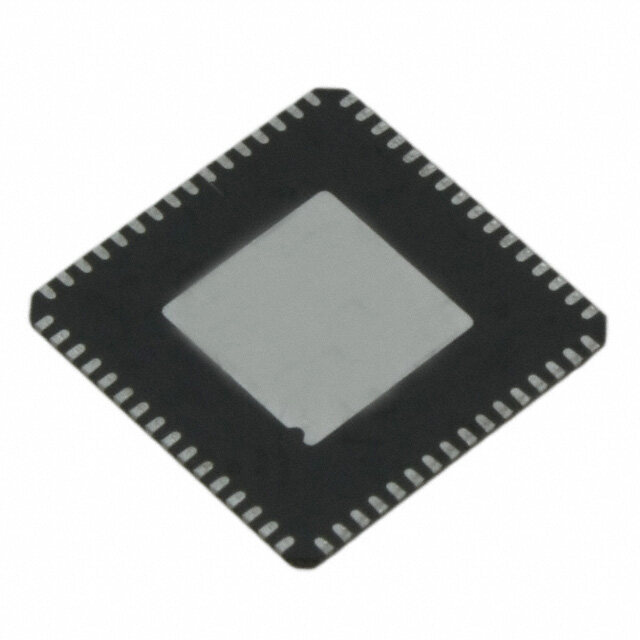
| 供应商器件封装 | 28-TQFN(4x4) |
| 包装 | 管件 |
| 商标 | Intersil |
| 安装类型 | 表面贴装 |
| 封装 | Tube |
| 封装/外壳 | 28-WFQFN 裸露焊盘 |
| 封装/箱体 | TQFN EP |
| 工作温度 | -10°C ~ 100°C |
| 工厂包装数量 | 75 |
| 应用 | 电源控制器,笔记本电脑 |
| 开关频率 | 28 kHz |
| 最大工作温度 | + 100 C |
| 最小工作温度 | - 10 C |
| 标准包装 | 75 |
| 电压-电源 | 5.5 V ~ 25 V |
| 电压-输入 | - |
| 电流-电源 | 150µA |
| 系列 | ISL62392 |
| 输出电压 | 0.6 V to 5.5 V, 0.6 V to 5.5 V |
| 输出电流 | 20 A, 20 A |
| 输出端数量 | 2 Output |
| 配用 | /product-detail/zh/ISL62392LOEVAL1Z/ISL62392LOEVAL1Z-ND/1975893/product-detail/zh/ISL62392HIEVAL1Z/ISL62392HIEVAL1Z-ND/1975892 |


PDF Datasheet 数据手册内容提取
DATASHEET ISL62391, ISL62392, ISL62391C, ISL62392C FN6666 High-Efficiency, Triple-Output System Power Supply Controller for Notebook Rev 8.00 Computers August 25, 2015 The ISL62391, ISL62392, ISL62391C and ISL62392C Features controller generate supply voltages for battery-powered • High Performance R3 Technology systems. It includes two pulse-width modulation (PWM) controllers, adjustable from 0.6V to 5.5V, and a linear • Fast Transient Response regulator (LDO3) that generates a fixed 3.3V and can deliver • ±1% Output Voltage Accuracy up to 100mA. The ISL62391, ISL62392, ISL62391C and ISL62392C include on-board power-up sequencing, a • 2 Fully Programmable Switch-Mode Power Supplies power-good (PGOOD) output, digital soft-start, and internal • Programmable Switching Frequency soft-stop output discharge that prevents negative voltages on shutdown. • Fixed 3.3V LDO Output The patented R3 PWM control scheme provides a low jitter • Internal Soft-Start and Soft-Stop Output Discharge system with fast response to load transients. Light-load • Wide Input Voltage Range: 5.5V to 25V efficiency is improved with period-stretching discontinuous • Full and Ultrasonic Pulse-Skipping Mode conduction mode (DCM) operation. To eliminate noise in audio frequency applications, an ultrasonic DCM mode is included, • Power-Good Indicator which limits the minimum switching frequency to 28kHz. • Overvoltage, Undervoltage and Overcurrent Protection The ISL62391, ISL62391C and ISL62392, ISL62392C are • Thermal Monitor and Protection identical except for how their overvoltage protection is • Pb-Free (RoHS Compliant) handled. The ISL62391 and ISL62391C utilize a tri-state overvoltage scheme, whereas the ISL62392 and ISL62392C Applications employ a soft-crowbar method. • Notebook and Sub-Notebook Computers The ISL62391, ISL62392, ISL62391C and ISL62392C are available in a 28Ld4x4 TQFN package and operate over • PDAs and Mobile Communication Devices the extended temperature range (-40°C to +100°C). • 3-Cell and 4-Cell Li+ Battery-Powered Devices Pinout ISL62391, ISL62392, ISL62391C, ISL62392C (28 LD 4X4 TQFN) TOP VIEW 2 2 2 2 T E E FB2 VOUT ISEN2 OCSE EN2 PHAS UGAT 28 27 26 25 24 23 22 PGOOD 1 21 BOOT2 FSET2 2 20 LGATE2 FCCM 3 19 PGND VCC 4 18 PVCC LDO3EN 5 17 VIN FSET1 6 16 LDO3 CENTER PAD: GND FB1 7 15 LGATE1 8 9 10 11 12 13 14 1 1 1 1 1 1 1 T N T N E E T U E E E S T O O S S A A O V I C H G B O P U FN6666 Rev 8.00 Page 1 of 22 August 25, 2015
ISL62391, ISL62392, ISL62391C, ISL62392C Ordering Information PART NUMBER PACKAGE PKG. (Notes 1, 2) PART MARKING TEMP RANGE (°C) (Pb-Free) DWG. # ISL62391HRTZ (Note 3) 623 91HRTZ -10 to +100 28 Ld 4x4 TQFN L28.4x4 ISL62392HRTZ (Note 3) 623 92HRTZ -10 to +100 28 Ld 4x4 TQFN L28.4x4 ISL62391CHRTZ (No longer available or 62391C HRTZ -10 to +100 28 Ld 4x4 TQFN L28.4x4 supported) ISL62392CHRTZ 62392C HRTZ -10 to +100 28 Ld 4x4 TQFN L28.4x4 ISL62391IRTZ (Note3) 623 91IRTZ -40 to +100 28 Ld 4x4 TQFN L28.4x4 ISL62392IRTZ (Note3) 623 92IRTZ -40 to +100 28 Ld 4x4 TQFN L28.4x4 ISL62391CIRTZ (No longer available or 62391C IRTZ -40 to +100 28 Ld 4x4 TQFN L28.4x4 supported) ISL62392CIRTZ 62392C IRTZ -40 to +100 28 Ld 4x4 TQFN L28.4x4 NOTES: 1. Add “-T*” suffix for tape and reel. Please refer to TB347 for details on reel specifications. 2. These Intersil Pb-free plastic packaged products employ special Pb-free material sets, molding compounds/die attach materials, and 100% matte tin plate plus anneal (e3 termination finish, which is RoHS compliant and compatible with both SnPb and Pb-free soldering operations). Intersil Pb-free products are MSL classified at Pb-free peak reflow temperatures that meet or exceed the Pb-free requirements of IPC/JEDEC J STD- 020. 3. Not Recommended for New Designs. No Recommended Replacement. FN6666 Rev 8.00 Page 2 of 22 August 25, 2015
ISL62391, ISL62392, ISL62391C, ISL62392C Absolute Maximum Ratings Thermal Information VIN to GND . . . . . . . . . . . . . . . . . . . . . . . . . . . . . . . . .-0.3V to +28V Thermal Resistance (Typical, Notes 4, 5) JA (°C/W) JC (°C/W) VCC, PGOOD, PVCC to GND. . . . . . . . . . . . . . . . . . -0.3V to +7.0V TQFN Package . . . . . . . . . . . . . . . . . . 37 3.5 EN1, 2, LDO3EN . . . . . . . . . . . . . . . . . . .-0.3V to GND, VCC +0.3V Junction Temperature Range. . . . . . . . . . . . . . . . . .-55C to +150°C VOUT1,2, FB1,2, FSET1,2 . . . . . . . . . . . .-0.3V to GND, VCC +0.3V Operating Temperature Range PHASE1,2 to GND. . . . . . . . . . . . . . . . . . . . . . . (DC) -0.3V to +28V ISL62391IRTZ). . . . . . . . . . . . . . . . . . . . . . . . . . .-40C to +100°C (<100ns Pulse Width, 10µJ). . . . . . . . . . . . . . . . . . . . . . . . . -5.0V ISL62392IRTZ). . . . . . . . . . . . . . . . . . . . . . . . . . .-40C to +100°C BOOT1,2 to GND. . . . . . . . . . . . . . . . . . . . . . . . . . . . .-0.3V to +33V Operating Temperature Range BOOT1,2 to PHASE1,2 . . . . . . . . . . . . . . . . . . . . . . . . .-0.3V to +7V ISL62391HRTZ). . . . . . . . . . . . . . . . . . . . . . . . . .-10C to +100°C UGATE1,2 . . . . . . . . . . . .(DC) -0.3V to PHASE1,2, BOOT1,2 +0.3V ISL62392HRTZ). . . . . . . . . . . . . . . . . . . . . . . . . .-10C to +100°C (<200ns Pulse Width, 20µJ) . . . . . . . . . . . . . . . . . . . . . . . . -4.0V Storage Temperature. . . . . . . . . . . . . . . . . . . . . . . .-65C to +150°C LGATE1,2. . . . . . . . . . . . . . . . . . . (DC) -0.3V to GND, PVCC +0.3V Pb-Free Reflow Profile. . . . . . . . . . . . . . . . . . . . . . . . .see link below (<100ns Pulse Width, 4µJ). . . . . . . . . . . . . . . . . . . . . . . . . . -2.0V http://www.intersil.com/pbfree/Pb-FreeReflow.asp LDO3 Current (Internal Regulator) Continuous . . . . . . . . . +100mA Recommended Operating Conditions Ambient Temperature Range ISL62391IRTZ). . . . . . . . . . . . . . . . . . . . . . . . . . .-40°C to +100°C ISL62392IRTZ). . . . . . . . . . . . . . . . . . . . . . . . . . .-40°C to +100°C Ambient Temperature Range ISL62391HRTZ). . . . . . . . . . . . . . . . . . . . . . . . . .-10°C to +100°C ISL62392HRTZ). . . . . . . . . . . . . . . . . . . . . . . . . .-10°C to +100°C Supply Voltage (VIN to GND) . . . . . . . . . . . . . . . . . . . . 5.5V to 25V CAUTION: Do not operate at or near the maximum ratings listed for extended periods of time. Exposure to such conditions may adversely impact product reliability and result in failures not covered by warranty. NOTES: 4. JA is measured in free air with the component mounted on a high effective thermal conductivity test board with “direct attach” features. See Tech Brief TB379. 5. For JC, the “case temp” location is the center of the exposed metal pad on the package underside. Electrical Specifications VIN=12V, EN=VCC, TA=-40°C to +100°C, unless otherwise noted. Typical values are at TA=+25°C. Boldface limits apply over the operating temperature range. MIN MAX PARAMETER CONDITIONS (Note 7) TYP (Note 7) UNITS LINEAR REGULATOR VIN Power-on Reset Rising Threshold 5.3 5.4 5.5 V Hysteresis 20 80 150 mV VIN Shutdown Supply Current EN1 = EN2 = LDO3EN = 0 6 15 µA VIN Standby Supply Current EN1 = EN2 = 0, LDO3EN = 1 150 250 µA LDO3 Output Voltage I_LDO3 = 100mA 3.25 3.3 3.35 V I_LDO3 = 0mA 3.25 3.3 3.35 V LDO3 Short-Circuit Current LDO3 = GND 180 mA LDO3EN Input Voltage Rising edge 1.1 2.5 V Falling edge 0.94 1.06 V LDO3EN Input Leakage Current LDO3EN = 0 or VCC -1 1 µA LDO3 Discharge ON-resistance LDO3EN = 0 36 60 PVCC POR Threshold 4.2 V SMPS2 to PVCC Switchover Threshold 4.63 4.8 4.93 V SMPS2 to PVCC Switchover Resistance VOUT2 to PVCC, VOUT2 = 5V 2.5 3.2 MAIN SMPS CONTROLLERS VCC Input Bias Current EN1 = EN2 = 1, FB1 = FB2 = 0.65V 2 mA VCC Start-up Voltage EN1 = EN2 = LDO3EN = GND 3.45 3.6 3.75 V FN6666 Rev 8.00 Page 3 of 22 August 25, 2015
ISL62391, ISL62392, ISL62391C, ISL62392C Electrical Specifications VIN=12V, EN=VCC, TA=-40°C to +100°C, unless otherwise noted. Typical values are at TA=+25°C. Boldface limits apply over the operating temperature range. (Continued) MIN MAX PARAMETER CONDITIONS (Note 7) TYP (Note 7) UNITS VCC POR Threshold Rising Edge 4.33 4.50 4.55 V Rising Edge (ISL62391HRTZ, ISL62392HRTZ, 4.35 4.50 4.55 V TA=-10°C to +100°C) Falling Edge 4.08 4.20 4.30 V Falling Edge (ISL62391HRTZ, ISL62392HRTZ, 4.10 4.20 4.30 V TA=-10°C to +100°C) Reference Voltage 0.6 V Regulation Accuracy VOUT regulated to 0.6V -1 1 % FB Input Bias Current FB = 0.6V -12 30 nA FB = 0.6V (ISL62391HRTZ, ISL62392HRTZ, -10 30 nA TA=-10°C to +100°C) Frequency Range 200 600 kHz Frequency Set Accuracy FSW = 300kHz (Note 6) -12 12 % VOUT Voltage Adjust Range VIN 6V for VOUT = 5.5V 0.6 5.5 V VOUT Soft-discharge Resistance 14 50 PGOOD Pull-down Impedance 32 50 PGOOD Leakage Current PGOOD = VCC 0 1 µA Maximum PGOOD Sink Current 5 mA PGOOD Soft-start Delay EN1 = EN2 = 1 2.20 2.75 3.70 ms (From first EN = 1 to PGOOD = 1) EN1 = 1, EN2 = Floating or EN1 = Floating, EN2 =1 4.50 5.60 7.60 ms EN1 = 1, EN2 = Floating or EN1 = Floating, EN2 =1 4.50 5.60 7.50 ms (ISL62391HRTZ, ISL62392HRTZ, TA=-10°C to +100°C) UGATE Pull-up ON-resistance 200mA source current 1.0 1.5 UGATE Source Current UGATE-PHASE = 2.5V 2.0 A UGATE Pull-down ON-resistance 250mA source current 1.0 1.5 UGATE Sink Current UGATE-PHASE = 2.5V 2.0 A LGATE Pull-up ON-resistance 250mA source current 1.0 1.5 LGATE Source Current LGATE-PGND = 2.5V 2.0 A LGATE Pull-down ON-resistance 250mA source current 0.5 0.9 LGATE Sink Current LGATE-PGND = 2.5V 4.0 A UGATE to LGATE Deadtime UG falling to LG rising, no load 21 ns LGATE to UGATE Deadtime LG falling to UG rising, no load 21 ns Bootstrap Diode Forward Voltage 2mA forward diode current 0.58 V Bootstrap Diode Reverse Leakage Current VR = 25V 0.2 1 µA FCCM Input Voltage Low Level (DCM enabled) 0.8 V Float Level (audio filter enabled) 1.9 2.1 V High Level (forced CCM) 2.4 V FCCM Input Leakage Current FCCM = GND or VCC -2 2 µA Audio Filter Switching Frequency FCCM floating 28 kHz EN Input Voltage Low Level (Clear fault level/SMPS off) 0.8 V Float Level (Delayed start) 1.9 2.1 V High Level (SMPS on) 2.4 V FN6666 Rev 8.00 Page 4 of 22 August 25, 2015
ISL62391, ISL62392, ISL62391C, ISL62392C Electrical Specifications VIN=12V, EN=VCC, TA=-40°C to +100°C, unless otherwise noted. Typical values are at TA=+25°C. Boldface limits apply over the operating temperature range. (Continued) MIN MAX PARAMETER CONDITIONS (Note 7) TYP (Note 7) UNITS EN Input Leakage Current EN = GND or VCC -3.5 3.5 µA ISEN Input Impedance EN = VCC 600 k ISEN Input Leakage Current EN = GND 0.1 µA OCSET Input Impedance EN = VCC 600 k OCSET Input Leakage Current EN = GND 0.1 µA OCSET Current Source EN = VCC 8.7 10.0 10.5 µA EN = VCC (ISL62391HRTZ, ISL62392HRTZ, 9 10.0 10.5 µA TA=-10°C to +100°C) OCP (OCSET-ISEN) Threshold -1.75 0.0 1.75 mV UVP Threshold Falling edge, referenced to FB 80.9 84 87 % Falling edge, referenced to FB (ISL62391HRTZ, 81 84 87 % ISL62392HRTZ, TA=-10°C to +100°C) OVP Threshold Rising edge, referenced to FB 113 116 120 % Falling edge, referenced to FB 99.5 103 106 % OTP Threshold Rising edge 150 °C Falling edge 135 NOTES: 6. FSW accuracy reflects IC tolerance only; it does not include frequency variation due to VIN, VOUT, LOUT, ESRCOUT, or other application specific parameters. 7. Compliance to datasheet limits is assured by one or more methods: production test, characterization and/or design. FN6666 Rev 8.00 Page 5 of 22 August 25, 2015
ISL62391, ISL62392, ISL62391C, ISL62392C Functional Pin Description PIN NAME FUNCTION 1 PGOOD Open-drain power-good status outputs. Connect to VCC through a 100k resistor. Output will be high when all outputs are within regulation with no faults detected. 2 FSET2 Frequency control input for SMPS2. Connect a resistor to ground to program the switching frequency. The pin output is a pulsed current and requires a decoupling capacitor to average the signal. 3 FCCM Logic input to control efficiency mode. Logic high forces continuous conduction mode (CCM). Logic low allows full discontinuous conduction mode (DCM). Float this pin for ultrasonic DCM operation. 4 VCC Analog power supply input for reference voltages and currents. Bypass to ground with a 1µF ceramic capacitor near the IC. 5 LDO3EN Logic input for enabling and disabling the LDO3 linear regulator. Positive logic input. 6 FSET1 Frequency control input for SMPS1. Connect a resistor to ground to program the switching frequency. The pin output is a pulsed current and requires a decoupling capacitor to average the signal. 7 FB1 SMPS1 feedback input used for output voltage programming and regulation. 8 VOUT1 SMPS1 output voltage sense input. Used for soft-discharge. 9 ISEN1 SMPS1 DCR current sense input. Used for overcurrent protection and R3 regulation. 10 OCSET1 Input from DCR current-sensing network used to program the overcurrent shutdown threshold for SMPS1. 11 EN1 Logic input to enable and disable SMPS1. A logic high will immediately enable SMPS1. Floating this pin will enable SMPS1 only after SMPS2 has been enabled and achieved regulation. A logic low disables SMPS1. 12 PHASE1 SMPS1 switching node for high-side gate drive return and synthetic ripple modulation. Connect to the switching NMOS source, the synchronous NMOS drain, and the output inductor for SMPS1. 13 UGATE1 High-side NMOS gate drive output for SMPS1. Connect to the gate of the SMPS1 switching FET. 14 BOOT1 SMPS1 bootstrap input for the switching NMOS gate drivers. Connect to SMPS1 PHASE with a ceramic capacitor of 0.22µF. 15 LGATE1 Low-side NMOS gate drive output for SMPS1. Connect to the gate of the SMPS1 synchronous FET. 16 LDO3 3.3V linear regulator output, capable of providing 100mA continuous current. Bypass to ground with a 4.7µF ceramic capacitor. 17 VIN Feed-forward input for line voltage transient compensation. Connect to the power train input voltage. 18 PVCC 5V power source for SMPS gate drive current. Bypass to ground with a 4.7µF ceramic capacitor. 19 PGND Power ground for SMPS1 and SMPS2. This provides a return path for synchronous FET switching currents. 20 LGATE2 Low-side NMOS gate drive output for SMPS2. Connect to the gate of the SMPS2 synchronous FET. 21 BOOT2 SMPS2 bootstrap input for the switching NMOS gate drivers. Connect to SMPS2 PHASE with a ceramic capacitor of 0.22µF. 22 UGATE2 High-side NMOS gate drive output for SMPS2. Connect to the gate of the SMPS2 switching FET. 23 PHASE2 SMPS2 switching node for high-side gate drive return and synthetic ripple modulation. Connect to the switching NMOS source, the synchronous NMOS drain, and the output inductor for SMPS2. 24 EN2 Logic input to enable and disable SMPS2. A logic high will immediately enable SMPS2. Floating this pin will enable SMPS2 only after SMPS1 has been enabled and achieved regulation. A logic low disables SMPS2. 25 OCSET2 Input from DCR current-sensing network used to program the overcurrent shutdown threshold for SMPS2. 26 ISEN2 SMPS2 DCR current sense input. Used for overcurrent protection and R3 regulation. 27 VOUT2 SMPS2 output voltage sense input. Used for soft-discharge and switchover for PVCC 5V LDO. 28 FB2 SMPS2 feedback input used for output voltage programming and regulation. Bottom GND Analog ground for analog and logic signals. Pad FN6666 Rev 8.00 Page 6 of 22 August 25, 2015
ISL62391, ISL62392, ISL62391C, ISL62392C Typical Application Circuits The typical application circuits generate the 5V/8A and 3.3V/8A (system regulator), or 1.05V/15A and 1.5V/15A (chip set) supplies in a notebook computer. The input supply (VBAT) range is 5.5V to 25V. VBAT 4x10µF BOOT1 VIN BOOT2 0.22µF 0.22µF 3.3V 4.7µH IRF7821 UGATE1 UGATE2 IRF7821 4.7µH 5V PHASE1 PHASE2 330µF 0.022µF14k 14k 0.022µF 330µF LGATE1 LGATE2 IRF7832 IRF7832 14k 14k 750 750 OCSET1 OCSET2 45.3k ISEN1 ISEN2 68.1k 1200pF 1200pF VOUT1 VOUT2 FB1 FB2 9.09k ISL62391, ISL62392 10k ISL62391C, ISL62392C 100k LDO3 PGOOD PVCC 4.7µF EN1 EN2 LDO3EN PVCC FCCM 1µF VCC FSET1 1µF FSET2 PGND PAD 24.3k 0.01µF 19.6k 0.01µF FIGURE 1. TYPICAL SYSTEM REGULATOR APPLICATION CIRCUIT WITH INDUCTOR DCR CURRENT SENSE VBAT BOOT1 VIN BOOT2 4x10µF 0.22µF IRF7821 IRF7821 0.22µF 3.3V 4.7µH UGATE1 UGATE2 4.7µH 0.001 5V PHASE1 PHASE2 330µF 0.001 1k IRF7832 IRF7832 330µF 1k LGATE1 LGATE2 1k 1k 750 750 OCSET1 OCSET2 1200pF 45.3k ISEN1 ISEN2 68.1k 1200pF VOUT1 VOUT2 FB1 FB2 9.09k 10k ISL62391, ISL62392 ISL62391C, ISL62392C 100k PGOOD PVCC 3.3V EN1 LDO3 EN2 LDO3EN 4.7µF PVCC FCCM 1µF VCC FSET1 1µF FSET2 PGND GND 24.3k 0.01µF 19.6k 0.01µF FIGURE 2. TYPICAL SYSTEM REGULATOR APPLICATION CIRCUIT WITH RESISTOR SENSE FN6666 Rev 8.00 Page 7 of 22 August 25, 2015
ISL62391, ISL62392, ISL62391C, ISL62392C Typical Application Circuits (Continued) VBAT 4x10µF BOOT1 VIN BOOT2 0.22µF 0.22µF IRF7821 IRF7821 1.05V 2.2µH 2x UGATE1 UGATE2 2x 2.2µH 1.5V PHASE1 PHASE2 2x330µF 0.022µF 14k 14k 0.022µF 2x330µF LGATE1 LGATE2 2x IRF7832 IRF7832 2x 14k 14k 590 590 OCSET1 OCSET2 1800pF 36.5k ISEN1 ISEN2 36.5k 1800pF VOUT1 VOUT2 FB1 FB2 48.7k ISL62391, ISL62392 24.3k ISL62391C, ISL62392C 100k LDO3 PGOOD PVCC 4.7µF EN1 EN2 LDO3EN PVCC FCCM 1µF VCC FSET1 1µF FSET2 PGND PAD 17.4k 0.01µF 14k 0.01µF FIGURE 3. TYPICAL CHIP SET APPLICATION CIRCUIT WITH INDUCTOR DCR CURRENT SENSE VBAT 4x10µF BOOT1 VIN BOOT2 0.22µF IRF7821 IRF7821 0.22µF 1.05V 2.2µH 2x UGATE1 UGATE2 2x 2.2µH 0.001 1.5V PHASE1 PHASE2 2x330µF 0.001 1k IRF7832 IRF7832 2x330µF 1k 2x LGATE1 LGATE2 2x 1k 1k 590 590 OCSET1 OCSET2 1800pF 36.5k ISEN1 ISEN2 36.5k 1800pF VOUT1 VOUT2 FB1 FB2 24.3k ISL62391, ISL62392 48.7k ISL62391C, ISL62392C 100k PGOOD PVCC 3.3V EN1 LDO3 EN2 LDO3EN 4.7µF PVCC FCCM 1µF VCC FSET1 1µF FSET2 PGND GND 17.4k 0.01µF 14k 0.01µF FIGURE 4. TYPICAL CHIP SET APPLICATION CIRCUIT WITH RESISTOR SENSE FN6666 Rev 8.00 Page 8 of 22 August 25, 2015
ISL62391, ISL62392, ISL62391C, ISL62392C Block Diagram VIN VOUT2* FSET1/2 4.8V 5V FB1/2 LDO R3 PVCC MODULATOR VREF 0.6V BOOT1/2 FCCM PWM UGATE UGATE1/2 DRIVER VOUT1/2 PHASE1/2 SOFT DISCHARGE LGATE DRIVER LGATE1/2 PGND EN1 START-UP PGOOD AND EN2 SHUTDOWN LOGIC LDO3EN VCC BIAS AND 10µA REFERENCE OCSET1/2 OCP T-PAD ISEN1/2 PROTECTION LOGIC OVP/UVP/OCP/OTP VREF + 16% UVP PVCC 3.3V FB1/2 LDO LDO3 OVP VREF - 16% THERMAL MONITOR SOFT DISCHARGE *In addition to being used for regulation, VOUT2 will also provide power for PVCC when it is programmed to 5V. FN6666 Rev 8.00 Page 9 of 22 August 25, 2015
ISL62391, ISL62392, ISL62391C, ISL62392C Typical Performance Curves 100 100 95 VIN = 7V 95 VIN = 7V 90 90 %) 85 VIN = 12V %) 85 VIN = 12V Y ( 80 VIN = 19V Y ( 80 VIN = 19V C C N 75 N 75 E E FICI 70 FICI 70 EF 65 EF 65 60 60 55 55 50 50 0.10 1.00 10.00 0.01 0.10 1.00 10.00 IOUT (A) IOUT (A) FIGURE 5. CHANNEL 1 EFFICIENCY AT VO=3.3V, DEM FIGURE 6. CHANNEL 2 EFFICIENCY AT VO=5V, DEM OPERATION. HIGH-SIDE 1xIRF7821, OPERATION. HIGH-SIDE 1xIRF7821, rDS(ON)=9.1m; LOW-SIDE 1xIRF7832, rDS(ON)=9.1m; LOW-SIDE 1xIRF7832, rDS(ON)=4m; L=4.7µH, DCR = 14.3m; CCM rDS(ON)=4m; L=4.7µH, DCR=14.3m; CCM FSW=270kHz FSW=330kHz VO1 VO1 FB1 FB1 PGOOD PGOOD PHASE1 PHASE1 FIGURE 7. POWER-ON, VIN=12V, LOAD=5A, VO=3.3V FIGURE 8. POWER-OFF, VIN=12V, IO=5A, VO=3.3V VO1 VO1 FB1 FB1 PGOOD PGOOD EN1 EN1 FIGURE 9. ENABLE CONTROL, EN1 = HIGH, VIN=12V, FIGURE 10. ENABLE CONTROL, EN1 = LOW, VIN=12V, VO=3.3V, IO=5A VO=3.3V, IO=5A FN6666 Rev 8.00 Page 10 of 22 August 25, 2015
ISL62391, ISL62392, ISL62391C, ISL62392C Typical Performance Curves (Continued) VO1 VO1 PHASE1 PHASE1 VO2 VO2 PHASE2 PHASE2 FIGURE 11. CCM STEADY-STATE OPERATION, VIN=12V, FIGURE 12. DCM STEADY-STATE OPERATION, VIN=12V, VO1=3.3V, IO1=5A, VO2=5V, IO2=5A VO1=3.3V, IO1= 0.2A, VO2=5V, IO2= 0.2A VO1 VO1 PHASE1 PHASE1 VO2 PHASE2 IO1 FIGURE 13. AUDIO FILTER OPERATION, VIN=12V, FIGURE 14. TRANSIENT RESPONSE, VIN=12V, VO=3.3V, VO1=3.3V, VO2=5V, NO LOAD IO=0.1A/8.1A @ 2.5A/µs VO1 VO1 PHASE1 PHASE1 IO1 IO1 FIGURE 15. LOAD INSERTION RESPONSE, VIN=12V, FIGURE 16. LOAD RELEASE RESPONSE, VIN=12V, VO=3.3V, IO=0.1A/8.1A @ 2.5A/µs VO=3.3V, IO=0.1A/8.1A @ 2.5A/µs FN6666 Rev 8.00 Page 11 of 22 August 25, 2015
ISL62391, ISL62392, ISL62391C, ISL62392C Typical Performance Curves (Continued) EN1 EN2 VO1 VO1 VO2 VO2 FIGURE 17. DELAYED START, VIN=12V, VO1=3.3V, VO2=5V, FIGURE 18. DELAYED START, VIN=12V, VO1=3.3V, VO2=5V, EN2 = FLOAT, NO LOAD EN1 = FLOAT, NO LOAD VO1 VO1 PGOOD IO1 VO2 PGOOD FIGURE 19. DELAYED START, VIN=12V, VO1=3.3V, VO2=5V, FIGURE 20. OVERCURRENT PROTECTION, VIN=12V, EN1 = 1, EN2 = FLOAT, NO LOAD VO=3.3V VO1 VO1 UGATE1-PHASE1 UGATE1-PHASE1 LGATE1 LGATE1 PGOOD PGOOD FIGURE 21. CROWBAR OVERVOLTAGE PROTECTION, FIGURE 22. TRI-STATE OVERVOLTAGE PROTECTION, VIN=12V, VO=3.3V, NO LOAD VIN=12V, VO=3.3V, NO LOAD FN6666 Rev 8.00 Page 12 of 22 August 25, 2015
ISL62391, ISL62392, ISL62391C, ISL62392C Theory of Operation A window voltage VW is referenced with respect to the error amplifier output voltage VCOMP, creating an envelope into Three Output Controller which the ripple voltage VR is compared. The amplitude of VW The ISL62391, ISL62392, ISL62391C and ISL62392C generate is set by a resistor, RW, connected across the FSET and GND three regulated output voltages. Two are produced with switch- pins. The VR, VCOMP, and VW signals feed into a window mode power supplies (SMPS), and the third by a low dropout comparator in which VCOMP is the lower threshold voltage and linear regulator (LDO). An additional 5V LDO (PVCC) is used to VW is the higher threshold voltage. Figure 23 shows PWM power the chip during operation, allowing the ISL62391, pulses being generated as VR traverses the VW and VCOMP ISL62392, ISL62391C and ISL62392C to regulate all outputs thresholds. The PWM switching frequency is proportional to from a single power source (VIN) with no need for a separate the slew rates of the positive and negative slopes of VR; it is quiescent supply. This makes the ISL62391, ISL62392, inversely proportional to the voltage between VW and VCOMP. ISL62391C and ISL62392C an ideal choice as system regulator Equation 3 illustrates how to calculate the window size based for notebook PCs. Because the two SMPS channels are on output voltage and frequency set resistor. identical and almost entirely independent, all conclusions drawn V = g V 1–DR (EQ. 3) apply to both channels unless otherwise noted. W m OUT W Modulator and Switching Frequency The frequency can be expressed in Equation 4: The ISL62391, ISL62392, ISL62391C and ISL62392C F = --------1---------- (EQ. 4) SW KR modulator feature Intersil’s R3 technology, a hybrid of fixed W frequency PWM and variable frequency hysteretic control. Inverting Equation 4 allows easy selection of RW for a desired Intersil’s R3 technology can simultaneously affect the PWM FSW: switching frequency and PWM duty cycle in response to input 1 voltage and output load transients. The R3 modulator RW = K---------F------------ (EQ. 5) SW synthesizes an AC signal, VR, which is an analog representation of the output inductor ripple current. The duty- For Equations 3 through 5: cycle of VR is the result of charge and discharge current gm = 1.66µs through a ripple capacitor, CR. The current through CR is K = 1.7 x 10⁻¹⁰ (±20%) provided by a transconductance amplifier that measures the VIN and VO pin voltages. The positive slope of VR can be D = VOUT/VIN written as Equation 1: Power-On Reset V = g V –V (EQ. 1) The ISL62391, ISL62392, ISL62391C and ISL62392C are RPOS m IN OUT disabled until the voltage at the VIN pin has increased above The negative slope of VR can be written as Equation 2: the rising power-on reset (POR) threshold. Conversely, the V = g V (EQ. 2) controller will be disabled when the voltage at the VIN pin RNEG m OUT decreases below the falling POR threshold. Where gm is the gain of the transconductance amplifier. In addition to VIN POR, the PVCC pin is also monitored. If its voltage falls below 4.2V, the SMPS outputs will be shut down. This ensures that there is sufficient BOOT voltage to enhance RIPPLE CAPACITOR VOLTAGE CR WIND(WORWT VVOCLOTMAPG)E VW the upper MOSFET. EN, Soft-Start and PGOOD The ISL62391, ISL62392, ISL62391C and ISL62392C use a digital soft-start circuit to ramp the output voltage of each SMPS to the programmed regulation setpoint at a predictable ERROR AMPLIFIER slew rate. The slew rate of the soft-start sequence has been VOLTAGE VCOMP selected to limit the in-rush current through the output capacitors as they charge to the desired regulation voltage. When the EN pins are pulled above their rising thresholds, the PWM PGOOD Soft-Start Delay, tSS, starts and the output voltage begins to rise. The FB pin ramps to 0.6V in approximately 1.5ms and the PGOOD pin goes to high impedance approximately 1.25ms after the FB pin voltage reaches 0.6V. FIGURE 23. MODULATOR WAVEFORMS DURING LOAD TRANSIENT FN6666 Rev 8.00 Page 13 of 22 August 25, 2015
ISL62391, ISL62392, ISL62391C, ISL62392C above the 4.2V VCC POR threshold, VCC will switchover to 1.5ms PVCC internally. tSOFTSTART VO After VIN is applied, the VCC start-up 3.6V voltage can be used VCC AND PVCC as the logic high signal of any of EN1, EN2 and LDO3EN to enable PVCC if there is no other power supply on the board. EN MOSFET Gate-Drive Outputs LGATE and UGATE FB The ISL62391, ISL62392, ISL62391C and ISL62392C have internal gate-drivers for the high-side and low-side N-Channel PGOOD MOSFETs. The low-side gate-drivers are optimized for low 2.75ms duty-cycle applications where the low-side MOSFET PGOOD DELAY conduction losses are dominant, requiring a low rDS(ON) MOSFET. The LGATE pull-down resistance is small in order to FIGURE 24. SOFT-START SEQUENCE FOR ONE SMPS clamp the gate of the MOSFET below the VGS(th) at turn-off. The The PGOOD pin indicates when the converter is capable of current transient through the gate at turn-off can be considerable supplying regulated voltage. It is an undefined impedance if VIN because the gate charge of a low rDS(ON) MOSFET can be large. is not above the rising POR threshold or below the POR falling Adaptive shoot-through protection prevents a gate-driver output threshold. When a fault is detected, the ISL62391, ISL62392, from turning on until the opposite gate-driver output has fallen ISL62391C and ISL62392C will turn on the open-drain NMOS, below approximately 1V. The dead-time shown in Figure 25 is which will pull PGOOD low with a nominal impedance of 32 extended by the additional period that the falling gate voltage This will flag the system that one of the output voltages is out of stays above the 1V threshold. The typical dead-time is 21ns. The regulation. high-side gate-driver output voltage is measured across the UGATE and PHASE pins while the low-side gate-driver output Separate enable pins allow for full soft-start sequencing. voltage is measured across the LGATE and PGND pins. The Because low shutdown quiescent current is necessary to power for the LGATE gate-driver is sourced directly from the prolong battery life in notebook applications, the PVCC 5V LDO PVCC pin. The power for the UGATE gate-driver is sourced from is held off until any of the three enable signals (EN1, EN2 or a “boot” capacitor connected across the BOOT and PHASE pins. LDO3EN) are pulled high. Soft-start of all outputs will only start The boot capacitor is charged from the 5V PVCC supply through until after PVCC is above the 4.2V POR threshold. In addition to a “boot diode” each time the low-side MOSFET turns on, pulling user-programmable sequencing, the ISL62391, ISL62392, the PHASE pin low. The ISL62391, ISL62392, ISL62391C and ISL62391C and ISL62392C include a pre-programmed ISL62392C have integrated boot diodes connected from the sequential SMPS soft-start feature. Table 1 shows the SMPS PVCC pins to BOOT pins. enable truth table. TABLE 1. SMPS ENABLE SEQUENCE LOGIC EN1 EN2 START-UP SEQUENCE tLGFUGR tUGFLGR 0 0 All SMPS outputs OFF 0 FLOAT All SMPS outputs OFF 50% 0 1 SMPS1 OFF, SMPS2 ON UGATE FLOAT 0 All SMPS outputs OFF FLOAT FLOAT All SMPS outputs OFF LGATE FLOAT 1 SMPS1 enables after SMPS2 is in regulation 50% 1 0 SMPS1 ON, SMPS2 OFF 1 FLOAT SMPS2 enables after SMPS1 is in regulation 1 1 All SMPS outputs ON simultaneously FIGURE 25. LGATE AND UGATE DEAD-TIME VCC Diode Emulation The VCC nominal operation voltage is 5V. If EN1, EN2 and LDO3EN are all logic low, the VCC start-up voltage is 3.6V FCCM is a logic input that controls the power state of the when VIN is applied on ISL62391, ISL62392, ISL62391C and ISL62391, ISL62392, ISL62391C and ISL62392C. If forced ISL62392C. PVCC is held off until any of the three enable high, the ISL62391, ISL62392, ISL62391C and ISL62392C will signals (EN1, EN2 or LDO3EN) is pulled high. When PVCC is operate in forced continuous-conduction-mode (CCM) over the entire load range. This will produce the best transient response FN6666 Rev 8.00 Page 14 of 22 August 25, 2015
ISL62391, ISL62392, ISL62391C, ISL62392C to all load conditions, but will have increased light-load power allow DEM at light loads, but will prevent the switching loss. If FCCM is forced low, the ISL62391, ISL62392, frequency from going below ~28kHz to prevent noise injection ISL62391C and ISL62392C will automatically operate in Diode to the audio band. A timer is reset each PWM pulse. If the Emulation Mode (DEM) at light load to optimize efficiency in the timer exceeds 30µs, LGATE is turned on, causing the ramp entire load range. The transition is automatically achieved by voltage to reduce until another UGATE is commanded by the detecting the load current and turning off LGATE when the voltage loop. inductor current reaches 0A. Overcurrent Protection Positive-going inductor current flows from either the source of The overcurrent protection (OCP) setpoint is programmed with the high-side MOSFET, or the drain of the low-side MOSFET. resistor, ROCSET, that is connected across the OCSET and Negative-going inductor current flows into the drain of the low- PHASE pins. side MOSFET. When the low-side MOSFET conducts positive inductor current, the phase voltage will be negative with L respect to the GND and PGND pins. Conversely, when the DCR IL VO low-side MOSFET conducts negative inductor current, the PHASE1 _ + VDCR phase voltage will be positive with respect to the GND and PGND pins. The ISL62391, ISL62392, ISL62391C and IISSLL6622339912, ROCSET CSEN CO ISL62392C monitor the phase voltage when the low-side MOSFET is conducting inductor current to determine its 10µAOCSET1 + VROCSET_ direction. RO When the output load current is greater than or equal to ½ the ISEN1 inductor ripple current, the inductor current is always positive, and the converter is always in CCM. The ISL62391, ISL62392, FIGURE 26. OVERCURRENT-SET CIRCUIT ISL62391C and ISL62392C minimize the conduction loss in Figure 26 shows the overcurrent-set circuit for SMPS1. The this condition by forcing the low-side MOSFET to operate as a inductor consists of inductance L and the DC resistance synchronous rectifier. (DCR). The inductor DC current IL creates a voltage drop across DCR, which is given by Equation 6: When the output load current is less than ½ the inductor ripple current, negative inductor current occurs. Sinking negative VDCR = ILDCR (EQ. 6) inductor through the low-side MOSFET lowers efficiency through unnecessary conduction losses. The ISL62391, The ISL62391, ISL62392, ISL62391C and ISL62392C sink a ISL62392, ISL62391C and ISL62392C automatically enter 10µA current into the OCSET1 pin, creating a DC voltage drop DEM after the PHASE pin has detected positive voltage and across the resistor ROCSET, which is given by Equation7: LGATE was allowed to go high for 8 consecutive PWM switching cycles. The ISL62391, ISL62392, ISL62391C and VROCSET = 10AROCSET (EQ. 7) ISL62392C will turn off the low-side MOSFET once the phase Resistor RO is connected between the ISEN1 pin and the voltage turns positive, indicating negative inductor current. The actual output voltage of the converter. During normal ISL62391, ISL62392, ISL62391C and ISL62392C will return to operation, the ISEN1 pin is a high impedance path, therefore CCM on the following cycle after the PHASE pin detects there is no voltage drop across RO. The DC voltage difference negative voltage, indicating that the body diode of the low-side between the OCSET1 pin and the ISEN1 pin can be MOSFET is conducting positive inductor current. established using Equation 8: Efficiency can be further improved with a reduction of unnecessary switching losses by reducing the PWM frequency. VOCSET1–VISEN1 = ILDCR–10AROCSET It is characteristic of the R3 architecture for the PWM (EQ. 8) frequency to decrease while in diode emulation. The extent of The ISL62391, ISL62392, ISL62391C and ISL62392C monitor the frequency reduction is proportional to the reduction of load the OCSET1 pin and the ISEN1 pin voltages. Once the current. Upon entering DEM, the PWM frequency makes an OCSET1 pin voltage is higher than the ISEN1 pin voltage for initial step-reduction because of a 33% step-increase of the more than 10µs, the ISL62391, ISL62392, ISL62391C and window voltage VW. ISL62392C declare an OCP fault. The value of ROCSET is then Because the switching frequency in DEM is a function of load written as Equation 9: cinutorr ethnet, avuedryio li gbhatn ldo.a Tdh ciso ncdainti obnes p craonb lpermodauticc eif fareuqduibelnec nieosis we eisll ROCSET = -I-O-----1C---0----D----A-C-----R--- (EQ. 9) coupled into audio amplifier circuits. To prevent this from occurring, the ISL62391, ISL62392, ISL62391C and ISL62392C allow the user to float the FCCM input. This will FN6666 Rev 8.00 Page 15 of 22 August 25, 2015
ISL62391, ISL62392, ISL62391C, ISL62392C Where: until the EN pin has been pulled below the falling EN threshold - ROCSET () is the resistor used to program the voltage, or until VIN has decayed below the falling POR overcurrent setpoint threshold. During the latch condition, the ISL62391 and - IOC is the output current threshold that will activate the ISL62391C will tri-state the PHASE node by turning both OCP circuit UGATE and LGATE off until the latch is cleared. - DCR is the inductor DC resistance Although latched, the ISL62392 and ISL62392C LGATE gate- For example, if IOC is 20A and DCR is 4.5m, the choice of driver output will retain the ability to toggle the low-side ROCSET is ROCSET = 20A x 4.5m/10µA = 9k MOSFET on and off in response to the output voltage transversing the OVP rising and falling thresholds. The LGATE Resistor ROCSET and capacitor CSEN form an R-C network to gate-driver will turn on the low-side MOSFET to discharge the sense the inductor current. To sense the inductor current output voltage, thus protecting the load from potentially correctly, not only in DC operation but also during dynamic damaging voltage levels. The LGATE gate-driver will turn off the operation, the R-C network time constant ROCSET-CSEN low-side MOSFET once the FB pin voltage is lower than the needs to match the inductor time constant L/DCR. The value of falling overvoltage threshold for more than 2µs. The falling CSEN is then written as Equation 10: overvoltage threshold is typically 106% of the reference voltage, L or 1.06*0.6V = 0.636V. This soft-crowbar process repeats as C = ----------------------------------------- SEN ROCSETDCR (EQ. 10) long as the output voltage fault is present, allowing the ISL62392 and ISL62392C to protect against persistent overvoltage For example, if L is 1.5µH, DCR is 4.5m, and ROCSET is 9k conditions. the choice of CSEN = 1.5µH/(9kx 4.5m) = 0.037µF Undervoltage Protection Upon converter start-up, the CSEN capacitor bias is 0V. To The UVP fault detection circuit triggers after the FB pin voltage is prevent false OCP during this time, a 10µA current source below the undervoltage threshold for more than 2µs. The flows out of the ISEN1 pin, generating a voltage drop on the undervoltage threshold is typically 86% of the reference voltage, RO resistor, which should be chosen to have the same or 0.86*0.6V = 0.516V. If a UVP fault is declared, the PGOOD resistance as ROCSET. When the PGOOD pin goes high, the pin will pull-down with 32and latch-off the converter. The fault ISEN1 pin current source will be removed. will remain latched until the EN pin has been pulled below the When an OCP fault is declared, the PGOOD pin will pull-down falling enable threshold, or if VIN has decayed below the falling to 32and latch-off the converter. The fault will remain latched POR threshold. until the EN pin has been pulled below the falling EN threshold Programming the Output Voltage voltage, or until VIN has decayed below the falling POR threshold. When the converter is in regulation, there will be 0.6V between the FB and GND pins. Connect a two-resistor voltage divider When using a discrete current sense resistor, inductor across the OUT and GND pins with the output node connected time-constant matching is not required. Equation 7 remains to the FB pin, as shown in Figure 27. Scale the voltage-divider unchanged, but Equation 8 is modified in Equation 11: network such that the FB pin is 0.6V with respect to the GND pin when the converter is regulating at the desired output VOCSET1–VISEN1 = ILRSENSE–10AROCSET (EQ. 11) voltage. The output voltage can be programmed from 0.6V to 5.5V. Furthermore, Equation 9 is changed in Equation 12: Programming the output voltage is written as Equation 13: ROCSET = I--O-----C-----1--R-0----S----EA----N----S----E-- (EQ. 12) VOUT = VREF1+R-----B--R--O---T-T--O--T---P-O----M---- (EQ. 13) Where RSENSE is the series power resistor for sensing inductor current. For example, with an RSENSE = 1m and an Where: OCP target of 10A, ROCSET = 1k - VOUT is the desired output voltage of the converter - The voltage to which the converter regulates the FB pin is Overvoltage Protection the VREF (0.6V) The OVP fault detection circuit triggers after the FB pin voltage - RTOP is the voltage-programming resistor that connects is above the rising overvoltage threshold for more than 2µs. from the FB pin to the converter output. In addition to The FB pin voltage is 0.6V in normal operation. The rising setting the output voltage, this resistor is part of the loop overvoltage threshold is typically 116% of that value, or compensation network 1.16*0.6V = 0.696V. - RBOTTOM is the voltage-programming resistor that connects from the FB pin to the GND pin For ISL62391, ISL62392, ISL62391C and ISL62392C, when an OVP fault is declared, the PGOOD pin will pull-down with 32 Choose RTOP first when compensating the control loop, and and latch-off the converter. The OVP fault will remain latched then calculate RBOTTOM according to Equation 14: FN6666 Rev 8.00 Page 16 of 22 August 25, 2015
ISL62391, ISL62392, ISL62391C, ISL62392C power dissipation. The outputs will remain off until the junction R = --V----R----E----F-------R----T----O----P---- (EQ. 14) temperature has fallen below +135°C. BOTTOM V –V OUT REF General Application Design Guide Compensation Design This design guide is intended to provide a high-level explanation Figure 27 shows the recommended Type-II compensation circuit. of the steps necessary to design a single-phase power The FB pin is the inverting input of the error amplifier. The COMP converter. It is assumed that the reader is familiar with many of signal, the output of the error amplifier, is inside the chip and the basic skills and techniques referenced in the following unavailable to users. CINT is a 100pF capacitor integrated inside section. In addition to this guide, Intersil provides complete the IC that connects across the FB pin and the COMP signal. reference designs that include schematics, bills of materials, and RTOP, RFB, CFB and CINT form the Type-II compensator. The example board layouts. frequency domain transfer function is given by Equation 15: 1+sRTOP+RFBCFB Selecting the LC Output Filter G s = ------------------------------------------------------------------------------------------- (EQ. 15) COMP sRTOPCINT1+sRFBCFB The duty cycle of an ideal buck converter is a function of the input and the output voltage. This relationship is written as Equation 16: CINT = 100pF RFB CFB D = -V-----O--- (EQ. 16) V IN RTOP The output inductor peak-to-peak ripple current is written as - VO FB Equation 17: COMP EA + RBOTTOM IPP = V-----O--f--S----W--1-----–-L---D------ (EQ. 17) REF A typical step-down DC/DC converter will have an IP-P of 20% ISL62391, ISL62392 to 40% of the maximum DC output load current. The value of IP-P is selected based upon several criteria, such as MOSFET FIGURE 27. COMPENSATION REFERENCE CIRCUIT switching loss, inductor core loss, and the resistive loss of the The LC output filter has a double pole at its resonant frequency inductor winding. The DC copper loss of the inductor can be that causes rapid phase change. The R3 modulator used in the estimated by Equation 18: ISL62391, ISL62392, ISL62391C and ISL62392C make the LC 2 PCOPPER = ILOAD DCR (EQ. 18) output filter resemble a first order system in which the closed loop stability can be achieved with the recommended Type-II Where ILOAD is the converter output DC current. compensation network. Intersil provides a PC-based tool The copper loss can be significant so attention has to be given (example page is shown later) that can be used to calculate to the DCR selection. Another factor to consider when compensation network component values and help simulate choosing the inductor is its saturation characteristics at the loop frequency response. elevated temperature. A saturated inductor could cause 3.3V Linear Regulator destruction of circuit components, as well as nuisance OCP faults. In addition to the two SMPS outputs, the ISL62391, ISL62392, ISL62391C and ISL62392C also provide a fixed 3.3V LDO output A DC/DC buck regulator must have output capacitance CO into (LDO3) capable of sourcing 100mA continuous current. LDO3 which ripple current IP-P can flow. Current IP-P develops a draws its power from PVCC and can be independently enabled corresponding ripple voltage VP-P across CO, which is the sum from both SMPS channels. of the voltage drop across the capacitor ESR and of the voltage change stemming from charge moved in and out of the LDO3 also has a current limit feature with a nominal level of capacitor. These two voltages are written as Equation 19: 180mA. Currents in excess of the limit will cause the LDO3 (EQ. 19) voltage to drop dramatically, limiting the power dissipation. VESR = IP-PESR Thermal Monitor and Protection and Equation 20: LDO3 and PVCC LDOs can dissipate non-trivial power inside the V = ----------I--P-------P----------- (EQ. 20) ISL62391, ISL62392, ISL62391C and ISL62392C at high input- C 8COfSW to-output voltage ratios and full load conditions. To protect the If the output of the converter has to support a load with high silicon, ISL62391, ISL62392, ISL62391C and ISL62392C pulsating current, several capacitors will need to be paralleled to continually monitor the die temperature. If the temperature exceeds +150°C, all outputs will be turned off to sharply curtail reduce the total ESR until the required VP-P is achieved. The inductance of the capacitor can cause a brief voltage dip if the FN6666 Rev 8.00 Page 17 of 22 August 25, 2015
ISL62391, ISL62392, ISL62391C, ISL62392C load transient has an extremely high slew rate. Low inductance MOSFET Selection and Considerations capacitors should be considered in this scenario. A capacitor Typically, a MOSFET cannot tolerate even brief excursions dissipates heat as a function of RMS current and frequency. Be beyond their maximum drain to source voltage rating. The sure that IP-P is shared by a sufficient quantity of paralleled MOSFETs used in the power stage of the converter should capacitors so that they operate below the maximum rated RMS have a maximum VDS rating that exceeds the sum of the upper current at fSW. Take into account that the rated value of a voltage tolerance of the input power source and the voltage capacitor can fade as much as 50% as the DC voltage across it spike that occurs when the MOSFET switches off. increases. There are several power MOSFETs readily available that are Selection of the Input Capacitor optimized for DC/DC converter applications. The preferred The important parameters for the bulk input capacitance are high-side MOSFET emphasizes low gate charge so that the the voltage rating and the RMS current rating. For reliable device spends the least amount of time dissipating power in operation, select bulk capacitors with voltage and current the linear region. Unlike the low-side MOSFET, which has the ratings above the maximum input voltage and capable of drain-source voltage clamped by its body diode during turn off, supplying the RMS current required by the switching circuit. the high-side MOSFET turns off with a VDS of approximately Their voltage rating should be at least 1.25x greater than the VIN-VOUT, plus the spike across it. The preferred low-side maximum input voltage, while a voltage rating of 1.5x is a MOSFET emphasizes low rDS(ON) when fully saturated to preferred rating. Figure 28 is a graph of the input RMS ripple minimize conduction loss. It should be noted that this is an current (normalized relative to output load current) as a function optimal configuration of MOSFET selection for low duty cycle of duty cycle and is adjusted for a converter efficiency of 80%. applications (D < 50%). For higher output, low input voltage The ripple current calculation is written as Equation21: solutions, a more balanced MOSFET selection for high- and 2 low-side devices may be warranted. I = D–D2+D-x----- (EQ. 21) IN_RMSNORMALIZED 12 For the low-side (LS) MOSFET, the power loss can be assumed to be conductive only and is written as Equation 23: Where: 2 - IMAX is the maximum continuous ILOAD of the converter PCON_LSILOAD rDSON_LS1–D (EQ. 23) - x is a multiplier (0 to 1) corresponding to the inductor peak-to-peak ripple amplitude expressed as a percentage For the high-side (HS) MOSFET, the conduction loss is written of IMAX (0% to 100%) as Equation 24: - D is the duty cycle that is adjusted to take into account the 2 efficiency of the converter which is written as Equation 22. PCON_HS = ILOAD rDSON_HSD (EQ. 24) V D = --------------O------------ (EQ. 22) For the high-side MOSFET, the switching loss is written as V EFF IN Equation 25: In addition to the bulk capacitance, some low ESL ceramic capacitance is recommended to decouple between the drain of VINIVALLEYtONfSW VINIPEAKtOFFfSW P = -----------------------------------------------------------------+------------------------------------------------------------- the high-side MOSFET and the source of the low-side SW_HS 2 2 MOSFET. (EQ. 25) Where: T N 0.60 - IVALLEY is the difference of the DC component of the E RR 0.55 inductor current minus 1/2 of the inductor ripple current U C 0.50 - IPEAK is the sum of the DC component of the inductor LE 0.45 current plus 1/2 of the inductor ripple current P RIP 0.40 - tON is the time required to drive the device into saturation MS 0.35 - tOFF is the time required to drive the device into cut-off R 0.30 T x = 1 Selecting The Bootstrap Capacitor PU 0.25 x = 0.75 N x = 0.50 The selection of the bootstrap capacitor is written as Equation D I 0.20 x = 0.25 ZE 0.15 x = 0 26: LI A 0.10 Q ORM 0.05 CBOOT = -----V----B----O-g---O-----T-- (EQ. 26) N 0 0 0.1 0.2 0.3 0.4 0.5 0.6 0.7 0.8 0.9 1.0 DUTY CYCLE FIGURE 28. NORMALIZED RMS INPUT CURRENT FN6666 Rev 8.00 Page 18 of 22 August 25, 2015
ISL62391, ISL62392, ISL62391C, ISL62392C Where: Co - Qg is the total gate charge required to turn on the high-side MOSFET PIN 18 (PVCC) L2 - VBOOT, is the maximum allowed voltage decay across PIN 4 (VCC) the boot capacitor each time the high-side MOSFET is L2 U2 switched on ISL6239 Ci As an example, suppose the high-side MOSFET has a total LINE OF SYMMETRY gate charge Qg, of 25nC at VGS=5V, and a VBOOT of 200mV. The calculated bootstrap capacitance is 0.125µF; for a Ci comfortable margin, select a capacitor that is double the calculated capacitance. In this example, 0.22µF will suffice. L1 U1 Use an X7R or X5R ceramic capacitor. PGND PLANE L1 Layout Considerations PHASE PLANES VOUT PLANES As a general rule, power should be on the bottom layer of the VIN PLANE Co PCB and weak analog or logic signals are on the top layer of FIGURE 30. SYMMETRIC LAYOUT GUIDE the PCB. The ground-plane layer should be adjacent to the top layer to provide shielding. The ground plane layer should have VIN (Pin 17) an island located under the IC, the compensation components, The VIN pin should be connected close to the drain of the high- and the FSET components. The island should be connected to side MOSFET, using a low resistance and low inductance path. the rest of the ground plane layer at one point. VCC (Pin 4) VVIIAASS T TOO GGNNDD GROUND GROUND OOUUTTPPUUTT For best performance, place the decoupling capacitor very PLANE PLANE CCAAPPAACCIITTOORRSS close to the VCC and GND pins. SSCCHHOOTTTTKKYY VOUT DDIIOODDEE PVCC (Pin 18) ININDDUUCCTTOORR PPNNHHOOAADDSSEEEE LMOLMOOWOSWS-FSF-ESEITDITDSESE For best performance, place the decoupling capacitor very close to the PVCC and respective PGND pin, preferably on the HHIIGGHH-S-SIDIDEE MMOOSSFEFTESTS INIPNPUUTT same side of the PCB as the ISL62391, ISL62392, ISL62391C VVININ CACAPPAACCITITOORRSS and ISL62392C ICs. FIGURE 29. TYPICAL POWER COMPONENT PLACEMENT EN (Pins 11 and 24), and PGOOD (Pin 1) Because there are two SMPS outputs and only one PGND pin, These are logic signals that are referenced to the GND pin. the power train of both channels should be laid out Treat as a typical logic signal. symmetrically. The line of bilateral symmetry should be drawn OCSET (Pins 10 and 25) and ISEN (Pins 9 and 26) through pins 4 and 18. This layout approach ensures that the For DCR current sensing, the current-sense network, controller does not favor one channel over another during critical switching decisions. Figure 29 illustrates one example consisting of ROCSET and CSEN, needs to be connected to the of how to achieve proper bilateral symmetry. inductor pads for accurate measurement. Connect ROCSET to the phase-node side pad of the inductor, and connect CSEN to Signal Ground and Power Ground the output side pad of the inductor. The ISEN resistor should The bottom of the ISL62391, ISL62392, ISL62391C and also be connected to the output pad of the inductor with a ISL62392C TQFN package is the signal ground (GND) separate trace. Connect the OCSET pin to the common node terminal for analog and logic signals of the IC. Connect the of node of ROCSET and CSEN. GND pad of the ISL62391, ISL62392, ISL62391C and For resistive current sensing, connect ROCSET from the ISL62392C to the island of ground plane under the top layer OCSET pin to the inductor side of the resistor pad. The ISEN using several vias for a robust thermal and electrical resistor should be connected to the VOUT side of the resistor conduction path. Connect the input capacitors, the output pad. capacitors, and the source of the lower MOSFETs to the power ground plane. In both current-sense configurations, the resistor and capacitor sensing elements, with the exclusion of the current sense PGND (Pin 19) power resistor, should be placed near the corresponding IC This is the return path for the pull-down of the LGATE low-side pin. The trace connections to the inductor or sensing resistor MOSFET gate driver. Ideally, PGND should be connected to should be treated as Kelvin connections. the source of the low-side MOSFET with a low-resistance, low- inductance path. FN6666 Rev 8.00 Page 19 of 22 August 25, 2015
ISL62391, ISL62392, ISL62391C, ISL62392C FB (Pins 7 and 28), and VOUT (Pins 8 and 27) BOOT (Pins 14 and 21), UGATE (Pins 13 and 22), and The VOUT pin is used to generate the R3 synthetic ramp PHASE (Pins 12 and 23) voltage and for soft-discharge of the output voltage during The signals going through these traces are both high dv/dt and shutdown events. This signal should be routed as close to the high di/dt, with high peak charging and discharging current. regulation point as possible. The input impedance of the FB pin Route the UGATE and PHASE pins in parallel with short and is high, so place the voltage programming and loop wide traces. There should be no other weak signal traces in compensation components close to the VOUT, FB, and GND proximity with these traces on any layer. pins, keeping the high impedance trace short. Copper Size for the Phase Node FSET (Pins 2 and 6) The parasitic capacitance and parasitic inductance of the This pin requires a quiet environment. The resistor RFSET and phase node should be kept very low to minimize ringing. It is capacitor CFSET should be placed directly adjacent to this pin. best to limit the size of the PHASE node copper in strict Keep fast moving nodes away from this pin. accordance with the current and thermal management of the application. An MLCC should be connected directly across the LGATE (Pins 15 and 20) drain of the upper MOSFET and the source of the lower The signal going through this trace is both high dv/dt and high MOSFET to suppress the turn-off voltage spike. di/dt, with high peak charging and discharging current. Route this trace in parallel with the trace from the PGND pin. These two traces should be short, wide, and away from other traces. There should be no other weak signal traces in proximity with these traces on any layer. FN6666 Rev 8.00 Page 20 of 22 August 25, 2015
ISL62391, ISL62392, ISL62391C, ISL62392C Revision History The revision history provided is for informational purposes only and is believed to be accurate, but not warranted. Please go to the web to make sure that you have the latest revision. DATE REVISION CHANGE August 25, 2015 FN6666.8 Updated Ordering Information table on page2. Added Revision History and About Intersil sections. Updated Package Outline Drawing L28.4X4 to the latest revision. -Revision 0 to Revision 1 changes - Added +/- 0.05 tolerances to each dimension in Top View and Bottom View. Added 2 degrees to Bottom view pin 1 index area dimension About Intersil Intersil Corporation is a leading provider of innovative power management and precision analog solutions. The company's products address some of the largest markets within the industrial and infrastructure, mobile computing and high-end consumer markets. For the most updated datasheet, application notes, related documentation and related parts, please see the respective product information page found at www.intersil.com. You may report errors or suggestions for improving this datasheet by visiting www.intersil.com/ask. Reliability reports are also available from our website at www.intersil.com/support. © Copyright Intersil Americas LLC 2008-2015. All Rights Reserved. All trademarks and registered trademarks are the property of their respective owners. For additional products, see www.intersil.com/en/products.html Intersil products are manufactured, assembled and tested utilizing ISO9001 quality systems as noted in the quality certifications found at www.intersil.com/en/support/qualandreliability.html Intersil products are sold by description only. Intersil may modify the circuit design and/or specifications of products at any time without notice, provided that such modification does not, in Intersil's sole judgment, affect the form, fit or function of the product. Accordingly, the reader is cautioned to verify that datasheets are current before placing orders. Information furnished by Intersil is believed to be accurate and reliable. However, no responsibility is assumed by Intersil or its subsidiaries for its use; nor for any infringements of patents or other rights of third parties which may result from its use. No license is granted by implication or otherwise under any patent or patent rights of Intersil or its subsidiaries. For information regarding Intersil Corporation and its products, see www.intersil.com FN6666 Rev 8.00 Page 21 of 22 August 25, 2015
ISL62391, ISL62392, ISL62391C, ISL62392C Package Outline Drawing L28.4x4 28 LEAD THIN QUAD FLAT NO-LEAD PLASTIC PACKAGE Rev 1, 6/15 4.00 ±0.05 A 2.50 ±0.05 PIN #1 INDEX AREA PIN 1 B 0.40 ±0.05 CHAMFER INDEX AREA 22 28 0.400 ±0.05 x 45° ±2° 21 1 F E 4.00 ±0.05 2.50 ±0.05 0.40 ±0.05x 6 = 2.40 R 3.20 ±0.05 4 0. 15 7 0.10 2x 14 8 0.20 ±0.05 0.10 M C A B 0.4 x 6 = 2.40 REF TOP VIEW 3.20 ±0.05 BOTTOM VIEW SEE DETAIL X'' 0.10 C (3.20) PACKAGE C OUTLINE MAX. 0.80 SEATING PLANE (28x 0.20) 0.00 - 0.05 0.20 REF 0.08 C SIDE VIEW 0) 0) 5 2 2. 3. ( ( (0.40) 0.20 REF C 5 (0.40) 0 ~ 0.05 (2.50) (28x 0.60) DETAIL "X" TYPICAL RECOMMENDED LAND PATTERN NOTES: 1. Controlling dimensions are in mm. Dimensions in ( ) are for reference only. 2. Unless otherwise specified, tolerance : Decimal ±0.05 Angular ±2° 3. Dimensioning and tolerancing conform to AMSE Y14.5M-1994. 4. Bottom side Pin#1 ID is diepad chamfer as shown. 5. Tiebar shown (if present) is a non-functional feature. FN6666 Rev 8.00 Page 22 of 22 August 25, 2015