ICGOO在线商城 > 开发板,套件,编程器 > 评估板 - 运算放大器 > ISL55210IRTZ-EVALZ

 Datasheet下载
- 型号: ISL55210IRTZ-EVALZ
- 制造商: Intersil
- 库位|库存: xxxx|xxxx
- 要求:
| 数量阶梯 | 香港交货 | 国内含税 |
| +xxxx | $xxxx | ¥xxxx |
查看当月历史价格
查看今年历史价格
ISL55210IRTZ-EVALZ产品简介:
ICGOO电子元器件商城为您提供ISL55210IRTZ-EVALZ由Intersil设计生产,在icgoo商城现货销售,并且可以通过原厂、代理商等渠道进行代购。 ISL55210IRTZ-EVALZ价格参考。IntersilISL55210IRTZ-EVALZ封装/规格:评估板 - 运算放大器, ISL55210 1 - Single Channels per IC Differential Amplifier Evaluation Board。您可以下载ISL55210IRTZ-EVALZ参考资料、Datasheet数据手册功能说明书,资料中有ISL55210IRTZ-EVALZ 详细功能的应用电路图电压和使用方法及教程。
Renesas Electronics America Inc.的ISL55210IRTZ-EVALZ是用于评估ISL55210运算放大器的评估板。该运算放大器属于高性能、低噪声、高速运算放大器,适用于对信号完整性要求较高的应用场景。

该评估板主要面向通信系统、工业自动化、测试与测量设备、医疗成像设备、高速数据采集系统等对信号处理性能要求较高的领域。例如,在通信基础设施中,可用于射频前端或中频放大;在工业控制中,可作为高精度传感器信号调理电路的一部分;在测试设备中,可作为高带宽、低失真信号处理链的关键组件。

该评估板设计便于用户快速评估ISL55210的电气性能,包括其带宽、噪声特性、失真水平及电源抑制比等关键参数。通过该评估板,工程师可以更高效地完成原型设计和系统验证,缩短开发周期。
| 参数 | 数值 |
| -3db带宽 | 2.2GHz |
| 产品目录 | 编程器,开发系统嵌入式解决方案 |
| 描述 | BOARD EVAL FOR ISL55210放大器 IC 开发工具 ISL55210I EVAL BOARD |
| 产品分类 | |
| 品牌 | Intersil |
| 产品手册 | |
| 产品图片 | |
| rohs | 符合RoHS无铅 / 符合限制有害物质指令(RoHS)规范要求 |
| 产品系列 | 模拟与数字IC开发工具,放大器 IC 开发工具,Intersil ISL55210IRTZ-EVALZ- |
| 数据手册 | |
| 产品型号 | ISL55210IRTZ-EVALZ |
| 产品 | Evaluation Boards |
| 产品种类 | 放大器 IC 开发工具 |
| 使用的IC/零件 | ISL55210 |
| 其它名称 | ISL55210IRTZEVALZ |
| 压摆率 | 5600 V/µs |
| 可用增益调整 | 100 dB |
| 商标 | Intersil |
| 封装 | Bulk |
| 工作温度 | -40°C ~ 85°C |
| 工作电源电压 | 3 V to 4.2 V |
| 工作电源电流 | 36 mA |
| 工具用于评估 | ISL55210 |
| 应用说明 | |
| 所含物品 | 板 |
| 描述/功能 | Wideband, low-power, ultra-high dynamic range differential amplifier |
| 放大器类型 | 差分 |
| 最大工作温度 | + 85 C |
| 最小工作温度 | - 40 C |
| 板类型 | 完全填充 |
| 标准包装 | 1 |
| 每IC通道数 | 1 - 单 |
| 用于 | ISL55210 |
| 电压-电源,单/双 (±) | 3 V ~ 4.2 V |
| 电流-电源(主IC) | 35mA |
| 电流-输出/通道 | 45mA |
| 类型 | Differential Amplifiers |
| 系列 | ISL55210 |
| 输出类型 | 差分 |


- 商务部:美国ITC正式对集成电路等产品启动337调查
- 曝三星4nm工艺存在良率问题 高通将骁龙8 Gen1或转产台积电
- 太阳诱电将投资9.5亿元在常州建新厂生产MLCC 预计2023年完工
- 英特尔发布欧洲新工厂建设计划 深化IDM 2.0 战略
- 台积电先进制程称霸业界 有大客户加持明年业绩稳了
- 达到5530亿美元!SIA预计今年全球半导体销售额将创下新高
- 英特尔拟将自动驾驶子公司Mobileye上市 估值或超500亿美元
- 三星加码芯片和SET,合并消费电子和移动部门,撤换高东真等 CEO
- 三星电子宣布重大人事变动 还合并消费电子和移动部门
- 海关总署:前11个月进口集成电路产品价值2.52万亿元 增长14.8%
PDF Datasheet 数据手册内容提取
DATASHEET ISL55210 FN7811 Wideband, Low-Power, Ultra-High Dynamic Range Differential Amplifier Rev 2.00 Jun 6, 2013 The ISL55210 is a very wide band, Fully Differential Amplifier Features (FDA) intended for high dynamic range ADC input interface applications. This voltage feedback FDA design includes an • Gain Bandwidth Product. . . . . . . . . . . . . . . . . . . . . . . . 4.0GHz independent output common mode voltage control. • Input Voltage Noise . . . . . . . . . . . . . . . . . . . . . . . 0.85nV/√(Hz) Intended for very high dynamic range ADC interface • Differential Slew Rate. . . . . . . . . . . . . . . . . . . . . . . 5,600V/µs applications, at the lowest quiescent power (115mW), the • 2VP-P, 2-tone IM3 (200Ω) 100MHz . . . . . . . . . . . . . . -109dBc ISL55210 offers a 4.0GHz Gain Bandwidth Product with a very • Supply Voltage Range . . . . . . . . . . . . . . . . . . . . . . 3.0V to 4.2V low input noise of 0.85nV/√(Hz). In a balanced differential I/O configuration, with 2VP-P output into a 200Ω load configured • Quiescent Power (3.3V Supply) . . . . . . . . . . . . . . . . . .115mW for a gain of 15dB, the IM3 terms are <-100dBc through Applications 110MHz. With a minimum operating gain of 2V/V (6dB), the ISL55210 supports a wide range of higher gains with minimal • Low Power, High Dynamic Range ADC Interface BW or SFDR degradation. Its ultra high differential slew rate of 5,600V/µs ensures clean large signal SFDR performance or a • Differential Mixer Output Amplifier fast settling step response. • SAW Filter Pre/Post Driver The ISL55210 requires only a single 3.3V (max 4.2V) power • Differential Comms-DAC Output Driver supply with 35mA typical quiescent current. This industry leading low current solution can be further reduced when Related Products and needed using the optional power shutdown to <0.4mA supply Literature current. External feedback and gain setting resistors give maximum flexibility and accuracy. A companion device, the •ISL55211 - Fixed Gain Version of the ISL55210 ISL55211, includes on-chip feedback and 3 possible gain •ISLA112P50 - 12-bit, 500MSPS ADC (<500mW) setting connections where an internally fixed gain solution is •ISLA214P50 - 14-bit, 500MSPS ADC (<850mW) preferred. The ISL55210 is available in a leadless, 16 Ld TQFN package and is specified for operation over the -40ºC to +85ºC •AN1649 - Designer’s Guide to the ISL55210 and ISL55211 ambient temperature range. Evaluation Boards •AN1725 - Ultra Low Power Broadband 8 to 14-Bit Data Acquisition Platform •AN1837 - Ultra High Performance Broadband 12 to 16-Bit Data Acquisition Platform •AN1831 - Designer's Guide to the ISL55210-ABEVAL1Z Active Balun Evaluation Board +3.3V 35mA 495 (115mW) SNRFS = 64.9dBFS 105MHz SINGLE TONE 180mVpp for -1dBFS 10k 500kHz 180MHz SPAN ISLA112P50 HHDD23 == --8834ddBBcc 12 Bit 100 + 40.2 V+ <500mW ENOBFS = 10.5 Bits Vi 1:2 0.1µF 33nH 20pF PD 210 50 0.1µF Vcm ISL55210 Vb Vdiff 210 ADT4-1WT 0.1µF 33nH 2V0p-F - 40.2 100 CLK 500MSPS Vdiff 20log ( )= 17.3dB gain 495 Vi FIGURE 1. TYPICAL APPLICATION CIRCUIT Pin Configuration FN7811 Rev 2.00 Page 1 of 19 Jun 6, 2013
ISL55210 ISL55210 (3x3 16 LD TQFN) TOP VIEW GND VS+ VCM GND 16 15 14 13 FB+ 1 12 VO+ Vi- 2 - 11 NC VCM Vi+ 3 + 10 NC FB- 4 9 VO- 5 6 7 8 GND VS+ GPNDD GND Pin Descriptions PIN NUMBER SYMBOL DESCRIPTION 1 FB+ Positive Output Feedback resistor connection 2 Vi- Inverting Amplifier Input 3 Vi+ Noninverting Amplifier Input 4 FB- Negative Output Feedback resistor connection 5, 8, 13, 16 GND Supply Ground (Thermal Pad Electrically Connected) 6, 15 VS+ Positive power supply (3.0V~4.5V) 7 PD Power-down: PD = logic low puts part into low power mode, PD = logic high or 1kΩ to VS+ for normal operation 9 VO- Inverting Amplifier Output 10, 11 NC No Internal Connection 12 VO+ Noninverting Amplifier Output 14 VCM Common-mode Voltage Input Ordering Information PART NUMBER TEMP RANGE PACKAGE TRANSPORT PKG. (Notes 1, 2, 3) PART MARKING (°C) (Pb-free) MEDIA, QUANTITY DWG. # ISL55210IRTZ 5210 -40 to +85 16 Ld 3x3 TQFN L16.3x3D ISL55210IRTZ-T7 5210 -40 to +85 16 Ld 3x3 TQFN Tape and Reel, 1000 L16.3x3D ISL55210IRTZ-T7A 5210 -40 to +85 16 Ld 3x3 TQFN Tape and Reel, 250 L16.3x3D ISL55210IRTZ-EVALZ Evaluation Board (Contact local sales) NOTES: 1. Please refer to TB347 for details on reel specifications. 2. These Intersil Pb-free plastic packaged products employ special Pb-free material sets, molding compounds/die attach materials, and 100% matte tin plate plus anneal (e3 termination finish, which is RoHS compliant and compatible with both SnPb and Pb-free soldering operations). Intersil Pb- free products are MSL classified at Pb-free peak reflow temperatures that meet or exceed the Pb-free requirements of IPC/JEDEC J STD-020. 3. For Moisture Sensitivity Level (MSL), please see device information page for ISL55210. For more information on MSL please see techbrief TB363. FN7811 Rev 2.00 Page 2 of 19 Jun 6, 2013
ISL55210 Absolute Maximum Ratings Thermal Information (TA = +25°C) Supply Voltage from VS+ to GND . . . . . . . . . . . . . . . . . . . . . . . . . . . . . . .4.5V Thermal Resistance (Typical) JA (°C/W) JC (°C/W) Input Voltage. . . . . . . . . . . . . . . . . . . . . . . . . . . . . . . .VS+ +0.3V to GND-0.3V 16 Ld TQFN Package (Notes 4, 5) . . . . . . . 63 16.5 Power Dissipation (See “Power Supply, Shutdown, and Thermal Storage Temperature. . . . . . . . . . . . . . . . . . . . . . . . . . . . . .-65°C to +125°C Considerations” on page13) Maximum Continuous Operating Junction Temperature. . . . . . . . . . .+135°C ESD Rating Pb-Free Reflow Profile . . . . . . . . . . . . . . . . . . . . . . . . . . . . . . . see link below Human Body Model (Per MIL-STD-883 Method 3015.7). . . . . . . .3500V http://www.intersil.com/pbfree/Pb-FreeReflow.asp Machine Model (Per EIAJ ED-4701 Method C-111) . . . . . . . . . . . . .250V Charged Device Model. . . . . . . . . . . . . . . . . . . . . . . . . . . . . . . . . . . .1500V Recommended Operating Conditions Latch up (Per JESD-78; Class II; Level A). . . . . . . . . . . . . . . . . . . . . . 100mA Ambient Operating Temperature . . . . . . . . . . . . . . . . . . . . .-40°C to +85°C CAUTION: Do not operate at or near the maximum ratings listed for extended periods of time. Exposure to such conditions may adversely impact product reliability and result in failures not covered by warranty. NOTES: 4. JA is measured in free air with the component mounted on a high effective thermal conductivity test board with “direct attach” features. See Tech Brief TB379. 5. For JC, the “case temp” location is the center of the exposed metal pad on the package underside. Electrical Specifications VS+ = +3.3V Test Conditions: G = 12dB, VCM = open, VO = 2VP-P, RF = 200Ω, RL = 200Ω differential, TA=+25°C, differential input, differential output, input and output referenced to internal default VCM (1.2V nominal) unless otherwise specified. MIN MAX TESTED PARAMETER CONDITIONS (Note 6) TYP (Note 6) UNIT (Note 7) AC PERFORMANCE Small-Signal Bandwidth (4-port S G = 12dB, VO = 100mVP-P 2,200 MHz parameter, Test Circuit #2) G = 18dB, VO = 100mVP-P 700 MHz G = 24dB, VO = 100mVP-P 300 MHz Gain-Bandwidth Product G = 18dB 4.0 GHz Bandwidth for 0.1-dB Flatness G = 12dB, VO = 100mVP-P 200 MHz Large-Signal Bandwidth G = 12dB, VO = 2VP-P 1.2 GHz Slew Rate (Differential) 5,600 V/µs Differential Rise/Fall Time 2-V step 0.17 ns 2nd-order Harmonic Distortion f = 20MHz, VO = 2VP-P -105 dBc f = 50MHz, VO = 2VP-P -88 dBc f = 100MHz, VO = 2VP-P -72 dBc 3rd-order Harmonic Distortion f = 20MHz, VO = 2VP-P -120 dBc f = 50MHz, VO = 2VP-P -107 dBc f = 100MHz, VO = 2VP-P -95 dBc 2nd-order Intermodulation Distortion fc = 70MHz, 200kHz spacing (2VP-P envelope) -80 dBc fc = 140MHz, 200kHz spacing (2VP-P envelope) -68 dBc 3rd-order Intermodulation Distortion fc = 70MHz, 200kHz spacing (2VP-P envelope) -102 dBc fc = 140MHz, 200kHz spacing (2VP-P envelope) -94 dBc Input Voltage Noise f > 1MHz, Differential 0.85 nV/√HZ Input Current Noise f > 1MHz, Each Input 5.0 pA/√HZ FN7811 Rev 2.00 Page 3 of 19 Jun 6, 2013
ISL55210 Electrical Specifications VS+ = +3.3V Test Conditions: G = 12dB, VCM = open, VO = 2VP-P, RF = 200Ω, RL = 200Ω differential, TA=+25°C, differential input, differential output, input and output referenced to internal default VCM (1.2V nominal) unless otherwise specified. (Continued) MIN MAX TESTED PARAMETER CONDITIONS (Note 6) TYP (Note 6) UNIT (Note 7) DC PERFORMANCE Open-loop Voltage Gain (AOL) Differential 86 100 dB * Input Offset Voltage TA = +25°C -1.4 ±0.1 +1.4 mV * TA = -40°C to +85°C -1.6 ±0.1 +1.6 mV Average Offset Voltage Drift TA = -40°C to +85°C ±3 µV/°C Input Bias Current TA = +25°C, positive current into the pin +50 +120 µA * TA = -40°C to +85°C +50 +140 µA Average Bias Current Drift TA = -40°C to +85°C +200 nA/°C Input Offset Current TA = +25°C -5 ±1 +5 µA * TA = -40°C to +85°C -6 ±1 +6 µA Average Offset Current Drift TA = -40°C to +85°C ±8 nA/°C INPUT Common-mode Input Range High 1.7 V * Common-mode Input Range Low 1.1 V * Common-mode Rejection Ratio f < 10MHz, common mode to differential 56 75 dB * output Differential Input Impedance 1 2 kΩpF OUTPUT Maximum Output Voltage Each output (with 200Ωdifferential load) 2.15 2.35 V * Linear Operation Minimum Output Voltage 0.45 0.63 V * Differential Output Voltage Swing TA = +25°C 3.04 3.8 VP-P * TA = -40°C to +85°C 2.95 V Differential Output Current Drive RL = 10Ω[sourcing or sinking] 40 45 mA * Closed-loop Output Impedance f < 10MHz, differential 0.6 Ω OUTPUT COMMON-MODE VOLTAGE CONTROL Small-signal Bandwidth From VCM pin to Output VCM 30 MHz Slew Rate Rising/Falling 150 V/µs Gain VCM input pin 1.0V to 1.4V 0.995 0.999 V/V * Output Common-Mode Offset from CM Input -8 ±1 +8 mV * CM Default Voltage Output VCM with VCM pin floating 1.18 1.2 1.22 V * CM Input Bias Current At control pin 2 µA CM Input Voltage Range At control pin 0.9 1.9 V * CM Input Impedance At control pin 1550 kΩpF POWER SUPPLY Specified Operation Voltage 3 3.3 4.2 V Quiescent Current TA = +25°, VS+ = 3.3V, VS- = 0V 33 35 37 mA * TA = -40°C to +85°C 30.5 36 39.5 mA Power-supply Rejection (PSRR) VS+ 3.0V - 4.5V range 56 90 dB * FN7811 Rev 2.00 Page 4 of 19 Jun 6, 2013
ISL55210 Electrical Specifications VS+ = +3.3V Test Conditions: G = 12dB, VCM = open, VO = 2VP-P, RF = 200Ω, RL = 200Ω differential, TA=+25°C, differential input, differential output, input and output referenced to internal default VCM (1.2V nominal) unless otherwise specified. (Continued) MIN MAX TESTED PARAMETER CONDITIONS (Note 6) TYP (Note 6) UNIT (Note 7) POWER-DOWN Referenced to GND Enable Voltage Threshold Assured on above 1.55V 1.3 1.55 V * Disable Voltage Threshold Assured off below 0.54V 0.54 0.7 V * Power-down Quiescent Current TA = +25°C 0.2 0.3 0.4 mA * TA = -40°C to +85°C 0.15 0.3 0.45 mA Input Bias Current PD = 0V, current positive into pin -2 µA Input Impedance 25 MΩpF Turn-on Time Delay Measured to output on 200 ns Turn-off Time Delay Measured to output off 400 ns NOTES: 6. Compliance to datasheet limits is assured by one or more methods: production test, characterization, and/or design. 7. Parameters denoted by an “*” are ATE tested. FN7811 Rev 2.00 Page 5 of 19 Jun 6, 2013
ISL55210 Typical Performance Curves VS+ = 3.3V, TA +25°C, unless otherwise noted. 6 18 3 VO = 3VP-P 15dB SLEW LIMITING 0 15 B) 21dB N (d -3 INPUT TRANSFORMER GAI -6 B) 12 ED -9 N (d VO = 1VP-P LIZ -12 27dB GAI 9 +2VP-P A M R -15 O N 33dB -18 6 -21 TEST CIRCUIT #1, RL = 200Ω, TEST CIRCUIT #1 VO = 500mVP-P DIFFERENTIAL -24 3 107 108 109 106 107 108 109 FREQUENCY (Hz) FREQUENCY (Hz) FIGURE 2. FREQUENCY RESPONSE vs GAIN SETTING FIGURE 3. FREQUENCY RESPONSE vs OUTPUT SWING -65 6.0 -75 NT 5.5 RIOUS (dBc) -85 IM2 21dBI MG2A I1N5dB GAIN ESSION POIRENTIAL) 5.0 RL =R 1L0 =0 Ω200Ω TONE IM SPU-1-0955 IM3 21dIBM 3G 1A5INdB GAIN TPUT COMPR(V, DIFFEP-P44..05 RL = 50Ω 2--115 OU 3.5 TEST CIRCUIT #1, RL = 200Ω, VOP-P = 1VP-P EACH TONE TEST CIRCUIT #1 -125 3.0 50 100 150 200 250 50 100 150 200 250 TEST FREQUENCIES CENTER (MHz) FREQUENCY (MHz) FIGURE 4. IM2 AND IM3 vs GAIN FIGURE 5. OUTPUT VP-P FOR -1dB GAIN COMPRESSION 12 12 11 11 GAIN = 15dB GAIN = 18dB B) B) d 10 d 10 RE ( RE ( GAIN = 24dB U U G 9 G 9 E FI GAIN = 21dB E FI S S OI 8 OI 8 N N 7 7 TEST CIRCUIT #1 WITH ADT4-1T INPUT AND RG = 100Ω, RF = 400Ω TEST CIRCUIT #1 6 6 50 200 350 500 50 200 350 500 FREQUENCY (MHz) FREQUENCY (MHz) FIGURE 6. NOISE FIGURE FIGURE 7. NOISE FIGURE AT HIGHER GAINS FN7811 Rev 2.00 Page 6 of 19 Jun 6, 2013
ISL55210 Typical Performance Curves VS+ = 3.3V, TA +25°C, unless otherwise noted. (Continued) -60 -60 TEST CIRCUIT #1, RL = 200Ω TEST CIRCUIT #1, RL = 200Ω -70 HD2 3VP-P c) -70 IM2 3VP-P US (dBc) -80 HD2 2VP-P OUS (dB -80 IM2 1VP-P IM2 2VP-P O HD3 3VP-P RI SPURI -90 HD2 1VP-P 3 SPU -90 IM3 3VP-P 3 M HD-100 D I -100 HD2/-110 HD3 1VP-P IM2 AN -110 IM3 2VP-P HD3 2VP-P IM3 1VP-P -120 -120 20 100 200 20 100 200 FREQUENCY (MHz) TEST FREQUENCIES CENTER (MHz) FIGURE 8. HD2/HD3 vs VOPP FIGURE 9. IM2 AND IM3 vs OUTPUT SWING -65 -60 TEST CIRCUIT #1 TEST CIRCUIT #1 Bc) -70 HD2, GAIN = 15dB c) -75 IM2 GAIN = 15dB d B ORTION ( -80 GAINH D=2 2,7dBHHDD22,, GGAAIINN == 2211ddBB RIOUS (d -85 IM3 GAIN = 21dB T U D3 DIS -90 GAINH D=3 1,5dB M3 SP -95 IM3 GAIN = 27dB ND H-100 HD3, AND I-105 IM3 GAIN = 27dB IM3 D2 A-110 GAIN = 21dB IM2 -115 GAIN = 21dB H IM3 GAIN = 15dB HD3, GAIN = 27dB -120 -125 20 100 200 20 100 200 FREQUENCY (MHz) TEST FREQUENCIES CENTER (MHz) FIGURE 10. HD2 AND HD3 vs GAIN FIGURE 11. IM2 AND IM3 vs GAIN -50 -50 HD2, 50Ω IM2, 100Ω -60 HD2, 100Ω -60 IM2, 50Ω c) -70 Bc) -70 B d N (d -80 HD2, 200Ω US ( -80 O HD3, 50Ω O IM3, 100Ω TI RI OR -90 HD2, 500Ω PU -90 T S DIS-100 HD3, 100Ω IM -100 IM2, 200Ω HD3, 200Ω IM3, 500Ω -110 -110 IM2, 500Ω HD3, 500Ω IM3, 200Ω -120 -120 20 100 200 20 100 200 FREQUENCY (MHz) CENTER FREQUENCY (MHz) FIGURE 12. HD2 AND HD3 vs RLOAD FIGURE 13. IM2 AND IM3 vs RLOAD FN7811 Rev 2.00 Page 7 of 19 Jun 6, 2013
ISL55210 Typical Performance Curves VS+ = 3.3V, TA +25°C, unless otherwise noted. (Continued) 180 1.7 10.0 GROUP DELAY, G = 27dB 165 1.6 D 150 1.5 ANz) IN (EACH INPUT) PHASE (°)11190320550 GRGO U=P 2 D1dEBLAY PHASE, G = 15dB 1111....1234ROUP DELAY (ns) GE NOISE (nV/√Hz) RENT NOISE (pA/√H1.0 EN (DIFFERENTIAL) G AR GROUP DELAY TU 75 G = 15dB PHASE 1.0 OLC G = 21dB V 60 PHASE 0.9 TEST CIRCUIT #2 G = 27dB 45 0.8 0.1 10 40 70 100 130 160 190 105 106 107 108 FREQUENCY (MHz) FREQUENCY (Hz) FIGURE 14. PHASE AND GROUP DELAY vs GAIN FIGURE 15. INPUT VOLTAGE AND CURRENT SPOT NOISE 3 10 N (dB) 0 RF = 402Ω RF = 200Ω CE (Ω) 9 SIMULATED TEST, TEST CIRCUIT #2 GAI -3 DAN 8 AL RF = 1.6kΩ PE 7 ERENTI --96 RF = 806Ω TPUT IM 56 GAINS 12dB TO 30dB F U D DIF -12 OP O 4 E O 3 NORMALIZ --1185 4-PORT S21 TEST, TEST CIRCUIT #2 CLOSED L 12 -21 0 107 108 109 1 10 100 1000 FREQUENCY (Hz) FREQUENCY (MHz) FIGURE 16. SMALL SIGNAL RESPONSE vs GAIN FIGURE 17. DIFFERENTIAL OUTPUT IMPEDANCE 3 -45 TEST CIRCUIT #3 COMMON MODE AC OUTPUT MEASUREMENTS 0 -50 B) -3 d 200mVP-P 10mVP-P (FF -55 B) -6 VDI d s AIN ( -9 vCM -60 G V -12 UT -65 P -15 UT O -70 -18 TEST CIRCUIT #3 COMMON MODE AC OUTPUT -21 -75 1 10 100 200 2 10 100 200 FREQUENCY (MHz) TEST FREQUENCY (MHz) FIGURE 18. VCM PIN INPUT FREQUENCY RESPONSE TO OUTPUT FIGURE 19. OUTPUT BALANCE ERROR COMMON MODE FN7811 Rev 2.00 Page 8 of 19 Jun 6, 2013
ISL55210 Typical Performance Curves VS+ = 3.3V, TA +25°C, unless otherwise noted. (Continued) 0.15 1.5 OUTPUT OUTPUT 0.10 1.0 V) 0.05 V) 0.5 E ( INPUT E ( INPUT D D U 0 U 0 T T LI LI P P M M A-0.05 A-0.5 -0.10 -1.0 TEST CIRCUIT #1, 50MHz SQUARE WAVE INPUT TEST CIRCUIT #1, 50MHz SQUARE WAVE INPUT -0.15 -1.5 0 10 20 30 40 50 0 5 10 15 20 25 30 35 40 45 50 TIMEBASE (ns) TIME (ns) FIGURE 20. SMALL SIGNAL STEP RESPONSE FIGURE 21. LARGE SIGNAL STEP RESPONSE 0 100MHz OUTPUT TEST CIRCUIT #1 -2 B) -4 100mVP-P INPUT d H ( -6 G U ENABLED RO -8 H PD DT-10 E E F-12 DISABLED 2VP-P INPUT -14 -16 TEST CIRCUIT #1 1 10 100 2µs/DIV FREQUENCY (MHz) FIGURE 22. ENABLE/DISABLE TIMES FIGURE 23. DISABLED FEEDTHROUGH 2.5 95 OUTPUT PSRR TO VO (DIFFERENTIAL) V) 2.0 S ( 85 M 1.5 R O EF 1.0 INPUT B) 75 WAF 0.5 R (d CMRR TO VO (DIFFERENTIAL) UT 0 MR 65 P C UT -0.5 RR/ D O -1.0 PS 55 N A UT -1.5 45 NP -2.0 TEST CIRCUIT #1 SIMULATED, I TEST CIRCUIT #1 EXACT EXTERNAL R’s -2.5 35 0 20 40 60 80 100 120 140 160 180 200 1 10 100 1000 TIME (ns) FREQUENCY (MHz) FIGURE 24. OVERDRIVE RECOVERY FIGURE 25. PSRR/CMRR TO DIFFERENTIAL VO FN7811 Rev 2.00 Page 9 of 19 Jun 6, 2013
ISL55210 Typical Performance Curves VS+ = 3.3V, TA +25°C, unless otherwise noted. (Continued) 6 45 TEST CIRCUIT #1 TEST CIRCUIT #1 44 43 TA = +85°C AND (V)P5 mA) 4412 EFAULT V CMRENTIAL VOP34 MOUATXPIMUUTM U SDIINFFGE DREEFNATUIALLT VVPC-MP Y CURRENT ( 3333467890 TA = +25°C DE L UTPUT AX DIFF 2 SUPP 333345 TA = -40°C OM 32 INTERNALLY SET VCM 31 1 30 3.0 3.1 3.2 3.3 3.4 3.5 3.6 3.7 3.8 3.9 4.0 4.1 4.2 4.3 4.4 4.5 3.0 3.1 3.2 3.3 3.4 3.5 3.6 3.7 3.8 3.9 4.0 4.1 4.2 4.3 4.4 4.5 SUPPLY VOLTAGE (V) SINGLE SUPPLY VOLTAGE (V) FIGURE 26. DEFAULT VCM AND MAX VOPP vs SUPPLY VOLTAGE FIGURE 27. SUPPLY CURRENT vs SUPPLY VOLTAGE Applications values. Since the ISL55210 is a VFA design, increasing the feedback resistor to get higher gain does not directly reduce the Basic Operation bandwidth as it would with a CFA based design. This gives increased flexibility in the input turns ratio and overall gain The ISL55210 is a very wideband, voltage feedback based, setting (while holding a matched input impedance) over differential amplifier including an output common mode control alternate solutions. loop and optional power shutdown feature. Intended for very low distortion differential signal driving, this non-unity gain stable +3.3V device also delivers extremely low input noise terms of 33mA 110mW 0.85nV/√Hz and 5pA/√Hz. Most applications are intended for AC 200 coupled I/O using a single 3.3V supply. It will operate over a RF 10k single supply range of 3.0V to 4.2V. Where DC coupled operation is desired, using split power supplies will allow the ISL55210 I/O 50 + 85 common mode range limits to be observed while giving either a 50 1:1.4 RG 1µF 35 1:1 50 differential I/O or single to differential configuration. VI 1µF 200 VCM PD VO2L0O0A D 1µF VM Most applications behave as a differential inverting op amp design. 0.1uF ISL55210 There is, therefore, an input gain resistor on each side of the inputs ADT2-1T 35 ADT1-1WT that must be driven. To retain overall low output noise, these RG - 1µF 85 resistors are normally of low value. The device can be powered down 50 to <400µA supply current using the optional disable pin. To operate RF normally, this pin should be asserted high using a simple logic gate 200 to +VS or tied high through a 10kΩ resistor to +VS. When disabled, FIGURE 28. TEST CIRCUIT #1 the power dissipation drops to <1mW but, due to the inverting op amp type architecture, the input signal will feed forward through the Working with a transformer coupled input as shown in Figure 28, external resistors giving limited isolation. or with two DC blocking caps from a differential source, means the output common mode voltage set by either the default Application and Characterization Circuits internal VCM setting, or a voltage applied to the VCM control pin, The circuit of Figure 28 forms a starting point for many of the will also appear as the input common mode voltage. This characterization curves for the ISL55210. Since most lab sources provides a very easy way to control the ISL55210 I/O common and measurement devices are single-ended, this circuit converts mode operating voltages for an AC coupled signal path. The to differential at the input through a wideband transformer and internal common mode loop holds the output pins to VCM and, would also be a typical application circuit coming from a single since there is no DC path for an ICM current back towards the ended source. Assuming the source is a 50Ω impedance, the RG input in Figure 28, that VCM setting will also appear as the input resistors are set to provide both the input termination and the common mode voltage. It is useful, for this reason, to leave any gain. Since the inverting summing nodes act as virtual ground input transformer secondary centertap unconnected. The points for AC signal analysis, the total termination impedance internally set VCM voltage is referenced from the negative supply across the input transformer secondary will be 2*RG. Setting pin. With a single 3.3V supply, it is very close to 1.2V but will this equal to n2*RS will give a matched input impedance inside change with total supply voltage across the device as shown in the bandwidth of the transformer (where "n" is the turns ratio). Figure 26. The amplifier gain is then set by adjusting the feedback resistors FN7811 Rev 2.00 Page 10 of 19 Jun 6, 2013
ISL55210 Most of the characterization curves start with Figure 28 then get impedance that increases with signal gain setting. The ISL55210 different gains by changing the feedback resistor, RF, use holds a more constant response vs gain due to internal design different input transformers where then the RG is also adjusted elements unique to this device. to hold an input match, or vary the loading. For load tests below Common mode output measurements are made using the circuit the 200Ω shown in Figure 28, a simple added shunt resistor is Figure 30. Here, the outputs are summed together through two placed across the output pins. For loads >200Ω, the series and 100Ω resistors (still a 200Ω differential load) to a center point shunt load R's are adjusted to show that total load (including the where the average, or common mode, output voltage may be 50Ω measurement load reflected through the 1:1 output sensed. This is coupled through a 1µF DC blocking capacitor and measurement port transformer) and provide an apparent 50Ω measured using 50Ω test equipment. The common mode source differential source to that transformer. This output side impedance for this circuit is the parallel combination of the transformer is for measurement purposes only and is not 2Ω-100Ω elements, or 50Ω. Figure 18 uses this circuit to necessary for final applications circuits. There are output interface designs that do benefit from a transformer as part of measure the small and large signal response from the VCM control pin to the output common mode. This pin includes an the signal path, but the one shown at the right of Figure 28 is internal 50pF capacitor on the default bias network (to filter used only for characterization to get a doubly terminated 50Ω supply noise when there is no connection to this pin) which measurement path going differential to single ended. bandlimits the response to approximately 30MHz. This is far Where just the amplifier is tested, a 4 port network analyzer is lower than the actual bandwidth of the common mode loop. used and the very simple test circuit of Figure 29 is Figure 19 uses this output CM measurement circuit with a large implemented. This is used to extract the differential S21 curves signal (2VP-P) differential output voltage (generated through the and differential output impedance vs gain. Changing the gain is a Vi path of Figure 30) to measure the differential to common simple matter of adjusting the two RF resistors of Figure 29. This mode conversion. circuit depends on the two AC coupled source 50Ω of the 4 port network analyzer and presents an AC coupled differential 100Ω +3.3V load to the amplifier as the input impedance of the remaining two ports of the network analyzer. 200 10k +3.3V 50 + 100 RF Vi 1:1.4 OUTPUT 10k PD VCM 1µF 50 1µF VCM ISL55210 50 50 + ADT2-1T 50 PD - S1/-2P AORFA AM 4E-pToErRt VCM ISL55210 1S/2-P OAFR AA M4-EPTOERRT 50 100 VCM INPUT 200 - 50 50 50 50 FIGURE 30. TEST CIRCUIT #3 COMMON MODE AC OUTPUT RF MEASUREMENTS FIGURE 29. TEST CIRCUIT #2 4-PORT S-PARAMETER MEASUREMENTS Single Supply, Input Transformer Coupled, Design Considerations Using this measurement allows the full small single bandwidth of the ISL55210 to be exposed. Many of the other measurements are The characterization circuit of Figure 28 shows one possible using I/O transformers that are limiting the apparent bandwidth to input stage interface that offers several advantages. The reduced level. Figure 16 shows a series of normalized differential ISL55210 can also support a DC coupled differential to S21 curves for gains of 12dB to 30dB in 6dB steps. These are differential or single ended input to differential requirement if simply stepping two feedback resistor values (RF) up from 200Ω to needed. Where AC coupling is adequate, the circuit of Figure 28 1600Ω in 2X steps. The lowest gain of 12dB (4V/V) is showing a simplifies the input common mode voltage control. If the source 2.2GHz small signal bandwidth. This response gets some coming into this stage is single ended, the input transformer bandwidth extension due to phase margin <60degree effects, but provides a zero power conversion to differential. The two gain by the gain of 24dB (16V/V), the bandwidth is following a Gain resistors (RG in Figure 28) provide both the input termination Bandwidth type characteristic showing 300MHz bandwidth or impedance and the gain element for the amplifier. For minimum >4GHz Gain Bandwidth Product (GBP). noise, only RG should be used and set to achieve the desired input impedance. Since the ISL55210 is a VFA device, these The closed loop differential output impedance of Figure 17 is resistor values can be scaled up and down a bit more freely than simulated using Figure 29 in ADS. This shows a relatively low a current feedback based FDA. output impedance (<1Ω through 100MHz) constant with signal gain setting. Typical FDA outputs show a closed loop output FN7811 Rev 2.00 Page 11 of 19 Jun 6, 2013
ISL55210 For instance, if a minimum noise configuration is not required, The examples shown are using the transformer to convert from but it is desirable to increase the feedback resistors to reduce the single to differential. However, if the source is already added loading they present to the output stage, the RG and RF differential, these same transformer input circuits can drive the resistors can be scaled up to achieve the same gain with an transformer differentially still providing impedance scaling if additional termination resistance added across the input needed and common mode rejection for both DC and AC transformer to adjust the termination impedance. Figure 31 common mode issues. A good example would be differential shows an example using a 1:2 input turns ratio where the RG and mixer outputs or SAW filter outputs. Those differential sources RF elements have been scaled up and a shunt termination could also be connected into the ISL55210 RG resistors through resistance added. This example provides a single to differential blocking caps as well eliminating the input transformer. The AC signal gain of 20dB and input impedance of 50Ω to the source. termination impedance for the differential source will then be The 1:2 turn ratio transformer needs a 200Ω differential the sum of the two RG resistors when simple blocking caps are secondary impedance to provide an input side 50Ω match. This is used. provided here by the parallel combination of the 2Ω-200Ω RG Amplifier I/O Range Limits resistors and the 400Ω parallel impedance at the transformer secondary. The ISL55210 is intended principally to give the lowest IM3 performance on the lowest power for a differential I/O +3.3V application. The amplifier will work DC coupled and over a relatively wide supply range of 3.0V to 4.2V supplies. The outputs 1k have both a differential and common mode operating range RF while the input pins have a common operating range. For single 200 supply operation, the ground pins are at ground as is the exposed + 50 1:2 RG metal pad on the underside of the package. The ISL55210 can operate split supply where then the ground pins will be a Vi 1µF 400 VCM ISL55210 VO negative supply voltage and the exposed metal pad is either connected to this negative supply or left unconnected on an ADT4- 1WT insulating board layer. RG - Briefly, the I/O and VCM limits are: 200 1. Maximum VCM setting = -VS + 2V RF 2. Input common mode operating range of -VS + 1.1V or the 1k output VCM + 0.5V FIGURE 31. SINGLE TO DIFFERENTIAL WITH REDUCED FEEDBACK 3. Output VO minimum (on each side) is either -VS + 0.3V or LOADING output VCM - 0.9V 4. Output VO maximum (on each side) is +VS - 1.5V This circuit has scaled the feedback resistor up to 1kΩ to still The output swing limits are often asymmetrical around the VCM achieve the amplifier gain of 5V/V which gives the overall gain of voltage. The maximum single ended swings are set by these two 10V/V (20dB) when the 1:2 step up at the input is considered. limits: The particular transformer shown is typical of 1:2 turns ratio broadband transformers, but there a many alternates with the VOMIN is either -VS + 0.3V or VCM - 0.9V whichever is less. So for similar or improved characteristics. instance on a single 3.3V supply with the default VCM voltage of 1.2V, these two limits give the same result and the output pins This input interface also simplifies the input common mode can swing down to 0.3V above -VS = 0V. If, however, the VCM pin control. The VCM pin controls the output common mode voltage. is raised to 1.5V, then the minimum output voltage will become In most DC coupled FDA applications, the input common mode 1.5V - 0.9V = 0.6V. voltage is determined by both this output common mode and the source signal. In a configuration like Figure 31, there is no path VOMAX is set by a headroom limit to the positive supply to be: for a common mode current to flow from output to input, so the input common mode voltage equals the output. A similar effect VOMAX = +VS - 1.5V. Again, on a 3.3V single supply and the could be achieved with just two blocking caps on the two RG dgreofuanudlt o1u.2tpVu VtC pMin s veottltinagg,e tsh cisa nm beea n3 .t3hVe -m1a.5xVim =u +m1 r.8eVfe orer n0c.e6dV to resistors. A DC coupled, single to differential, configuration will also have a common mode input that is moving with the input above the default VCM voltage. signal. Converting to just a differential signal at the amplifier, as Using these default conditions, and the maximum positive in Figure 31, removes any input signal related artifacts from the excursion of 0.6V above the 1.2V output VCM setting, the input common mode making the ISL55210 behave as a maximum differential VP-P swing will be 4X this 0.6V single differential only VFA amplifier. There is only a very small ended limit or 2.4VP-P. Where +VS is increased the limit then differential error signal at the inputs set by the loop gain, as in a becomes the 0.9V below VCM, but then the absolute maximum normal single ended VFA application, but no common mode differential VP-P is then 4X 0.9V to 3.6VP-P. So, for instance, to signal related terms. get this maximum output swing, increase the supply voltage until +VS - 1.5V > VCM + 0.9V. If we assume a VCM voltage of 1.3V for instance, then 1.3V + 0.9V + 1.5V = 3.7V will give an unclipped FN7811 Rev 2.00 Page 12 of 19 Jun 6, 2013
ISL55210 3.6VP-P output capability. The VP-P reported in Figure 26 is an +5V ±5% asymmetrically clipped maximum swing. Going 10% above this 3.7V target to 4.1V will be within the recommended operating 24.3 range and give some tolerancing headroom that would also 35 55mA 3.4 4.4V + 2.2µF suggest the VCM voltage be moved up to approximately 1.5V. This 10nF coincides with the default output VCM from Figure 26. Operating RF 10k at +4.1V single supply in a Figure 28 type configuration will give the maximum linear available output swing of 3.6VP-P. + Cin 1:n RG RO The differential inputs of the ISL55210 also have operating PD range limits relative to the supply voltages. Operating in an AC Vi VCM ISL55210 VO coupled circuit like Figure 28 will produce an input common mode voltage equal to the outputs. The inputs can operate with RO full linearity with this VCM voltage down to 1.1V above the GND RG - connection (or -VS supply). On the default 1.2V output VCM on +3.3V supplies this gives a 100mV guardband on the input VCM voltages. Overriding the default VCM by applying a control voltage RF to the VCM pin should be done with care in going towards the negative supply due to this limit. On the + side, the maximum FIGURE 32. OPERATING FROM A SINGLE +5V SUPPLY VCM above the -VS supply is 2V so there is more room to move the output VCM up than down from the default value. The ISL55210 includes a power shutdown feature that can be When operated as a DC coupled single to differential amplifier, used to reduce system power dissipation when signal path the input common mode voltage will move with the input signal operation is not required. This pin (PD) is referenced to the and will be different than the output common mode voltage ground pins and must be asserted low to activate the shutdown when the external resistors are set for gain. When the input feature. When not used, a 10kΩ external resistor to +VS should common mode can be different than the output, the additional be used to assert a high level at this pin. Digital control on this constraint that must be observed is that the input common mode pin can be either an open collector output (using that 10kΩ voltage cannot be > output VCM +0.5V. This would only occur if pullup) or a CMOS logic line running off the same +VS as the the single source was coming from a higher voltage than the amplifier. For split supply operation, the PD pins must be pulled output VCM setting. to below -VS + 0.54V to disable. Power Supply, Shutdown, and Thermal Since the ISL55210 operates as a differential inverting op amp, there is only modest signal path isolation when disabled as Considerations shown in Figure 23. For small input signals, Figure 23 shows The ISL55210 is intended for single supply operation from 3.0V about 5dB to 6dB isolation while for large signals, back to back to 4.2V with an absolute maximum setting of 4.5V. The 3.3V protection diodes across the inputs compress the signal to show supply current is trimmed to be nominally 35mA at +25°C actually an improved isolation. This is intended to protect any ambient. Figure 27 shows the supply current for nominal +25°C subsequent devices from large input signals during shutdown. and -40°C to +85°C operation over the specified maximum Those diodes limit the maximum overdrive voltage across the supply range. The input stage is biased from an internal voltage input to approximately 0.5V in each polarity. The RG resistors of referenced from the negative supply giving the exceptional 90dB Test Circuit #1 limit the current into those diodes under this low frequency PSRR shown in Figure 25. condition. Since the input stage bias is from a re-regulated internal supply, The supply current in shutdown does not reduce to zero as a simple approach to single +5V operation can be supported as internal circuitry is still active to hold the output common mode shown in Figure 32. Here, a simple IR drop from the +5V supply voltage at the VCM control input voltage even during shutdown (or will bring the operating supply voltage for the ISL55210 into its the default value). This is intended to hold the ISL55210 output allowed range. Figure 32 shows example calculations for the near the desired common mode output level during shutdown. voltage range at the ISL55210 +VS pin assuming a ±5% This improves turn on characteristic and keeps the output tolerance on the +5V supply and a 35mA to 55mA range on the voltages in a safe range for downstream circuitry. total supply current. Considering the 34mA to 44mA quiescent DISABLED OPERATION WARNING IN DC COUPLED DESIGNS current range from Figure 27 over the -40°C to +85°C ambient, When disabled, the output stage provides a nominal DC voltage and the 3.4V to 4.4V supply voltage range assumed here, this is at the Vcm control pin input or the default internal 1.2V value. designing for a 1mA to 11mA average load current which should Being very low power, any external circuit condition that can be adequate for most intended application loads. Good supply cause the output pins to source or sink DC current can move the decoupling at the device pins is required for this simple solution ISL55210 internal operating points into regions from which it to still provide exceptional SFDR performance. may not recover when the device is enabled. If the external circuitry can force >20µA into the output pins or pull > 1.5mA out of the output pins correct operation is not guaranteed. For designs that might force current into the output stage during disable, adding a resistor to ground on the outputs might provide FN7811 Rev 2.00 Page 13 of 19 Jun 6, 2013
ISL55210 an effective means of turning that into a low sourcing current With equal feedback and gain resistors, the total output noise condition with minimal impact to the desired signal path expression becomes very simple. This is: operation when enabled. 2 2 The very low internal power dissipation of the ISL55210, along e0 = eniNG +2inRf +24kTRfNG (EQ. 1) with the excellent thermal conductivity of the QFN package when the exposed metal pad is tied to a conductive plate, reduces the The NG term in Equation 1 is the Noise Gain = 1+RF/RG. The TJ rise above ambient to very modest levels. Assuming a nominal last term in Equation 1 captures both the RF and RG resistor 115mW dissipation and using the +63°C/W measured thermal noise terms. If we assume a 50Ω source in Test Circuit #1, the impedance from Junction to ambient, gives a rise of only total RG resistor value will be 100Ω as that 50Ω will come 0.12*63 = +7.6°C. Operation at elevated ambient through the transformer to look like a 50Ω source on each side. temperatures is easily supported given this very low internal rise This gives a lower noise gain (3V/V) than signal gain (4V/V) for to junction. just the amplifier. The total gain in Test Circuit #1 is still approximately 1.4 * 4 = 5.6V/V including the transformer step The maximum internal junction temperatures would occur at up. maximum supply voltage, +85°C maximum ambient operating, and where the QFN exposed pad is not tied to a conductive layer. Putting in NG = 3, RF = 200Ω, RG = 100Ω with the ISL55210 Where the QFN must be mounted with an insulating layer to the noise terms of eni = 0.85nV/√Hz and In = 5pA/√Hz into Equation1 exposed metal plate, such as in a split supply application, device (4kT= 1.6E-20J) gives a total output differential noise measurements show an increased thermal impedance junction voltage= 5.26nV/√Hz. Input referring this to the input side of the to ambient of +120°C/W. Using this, and a maximum quiescent transformer of Test Circuit #1 gives an input referred spot noise internal power on 4.5V absolute maximum, which shows 45mA of only 0.88nV/√Hz. This extremely low input referred noise is a for +85°C maximum operating ambient from Figure 27, we get combination of low amplifier noise terms and the effect of the 4.5V*45mA*+120°C/W = +24°C rise above +85°C or input transformer configuration. approximately +109°C operating TJ maximum - still well below Driving Cap and Filter Loads the specified Absolute Maximum operating junction temperature of +135°C. Most applications will drive a resistive or filter load. The ISL55210 is robust to direct capacitive load on the outputs up to Noise Analysis approximately 10pF. For frequency response flatness, it is best to The decompensated voltage feedback design of the ISL55210 avoid any output pin capacitance as much as possible - as that provides very low input voltage and current noise. While a capacitance increases, the high frequency portion of the detailed noise model using arbitrary external resistors can be ISL55210 (>1GHz) response will start to show considerable made, most applications will have a balanced feedback network peaking. No oscillations were observed up through 10pF load on with the two RF (feedback) resistors equal and the two RG (gain) each output. resistors equal. Figure 33 shows the test circuit used to measure For AC coupled applications, an output network that is a small the output noise with the noise terms detailed. The aim here was series resistor (10Ω to 50Ω) into a blocking cap is preferred. This to measure the output noise with two different resistor settings series resistor will isolate parasitic capacitance to ground from to extract out a model for the input referred En and In terms for the internally closed loop output stage of the amplifier and just the amplifier itself. de-queue the self resonance of the blocking capacitors. Once the output stage sees this resistive element first, the remaining part 4kT*Rf of the filter design can be done without fear of amplifier instability. RF 4kT*Rg eni + Driving ADCs 1µF RG in * 25 1:1 1µF Mpoawneyr o, vf ethrye hinigthen ddyenda mapicp lriacantgioe,n lsa fsot rs tthaeg eIS iLn5te5r2fa1c0e atore h aigsh a low ISL55210 eO ADT1-1WT 50 performance ADCs. The lowest power ADCs, such as the * ISLA112P50 shown on the front page, include an innovative in "Femto-Charge" internal architecture that eliminates op amps 25 4kT*Rg RG from the ADC design and only passes signal charge from stage to - stage. This greatly reduces the required quiescent power for 1µF these ADCs but then that signal charge has to be provided by the * RF external circuit at the two input pins. This appears on an ADC like the ISLA112P50 as a clock rate dependent common mode input 4kTRf current that must be supplied by the interface circuit. At 500MHz, this DC current is 1.3mA on each input for the FIGURE 33. NOISE MODEL AND TEST CIRCUIT ISLA112P50. Most interfaces will also include an interstage noise power bandlimiting filter between the amplifier and the ADC. This filter needs to be designed considering the loading of the amplifier, FN7811 Rev 2.00 Page 14 of 19 Jun 6, 2013
ISL55210 any VCM level shifting that needs to take place, the filter shape, the ADC inputs. These bias inductors do limit the low and this ICM issue into the ADC input pins. Here are 4 example frequency end of the operation where, with 1µH values, topologies suitable for different situations. operation from 10MHz to 200MHz is supported using the approach of Figure 35. 1. AC coupled, broadband RLC interstage filter design. This approach lets the amplifier operate at its desired output 3. AC coupled with output side transformer. This design includes common mode, then provides the ADC common mode an output side transformer, very similar to ADC voltage and current through a bias path as part of the filter characterization circuits. This approach allows a slightly lower design’s last stage R values. The VB is set to include the IR amplifier output swing (if N>1 is used) and very easy 2nd loss from that voltage to the ADC inputs due to the ICM order low pass responses to be implemented. It also provides current. This circuit is the one shown on the front page where the ICM and VCM bias to the ADC through the transformer we get a usable frequency range from about 500kHz to centertap. This approach would be attractive for higher ADC 150MHz. input swing targets and more aggressive noise power bandwidth control needs. 2. AC coupled, higher frequency range interstage filter design. This design replaces the Rt resistors in Figure 34 with large 4. DC coupled with ADC VCM and ICM provided from the valued inductors and implements the filter just using shunt amplifier. Here, DC to very high frequency interstage low pass resistors at the end of the RLC filter (here, that is just the ADC filters can be provided. Again, the RS element must be low to internal differential Rin). In this case, the ADC VCM can be tied reduce the IR drop from the VCM of the converter, which now to the centerpoint of the bias path inductors (very much like a shows up on the output of the ISL55210, to the ADC input Bias-T) to provide the common mode voltage and current to pins. In this case, split supplies are required to satisfy the amplifier output and input common mode range limits discussed earlier. Rf RF ADC ADC +3.3V Ls Icm IN+ +3.3V LS ICM IN+ ISL55210 Vcm1 1.2V Rs Cb Vb Rt Ct Rin Cin VCM1 ISL552101.2V RS Cb RT LP Ct RinCin Rs Cb Ls Rt Ct IN- RS Cb LS LP Ct Rf IN- RtRtRsRs Icm Vcm2o r= 10V.535 RF ICM VCM2 = 0.535 vB–VIbcmIcmRt=RtVcmVc2m 2 or 1V LpLs FIGURE 34. AC COUPLED, BROADBAND RLC INTERSTAGE FILTER DE FIGURE 35. AC COUPLED, HIGHER FREQUENCY RLC FILTER DESIGN SIGN RF Rf ADC ADC +3.3V ICM +3.0V Ls Icm IN+ IN+ ISL55210 ISL55210 RS Cb 1:n Rt Rs VCM1 1.2V Ct Cin Vcm Ct Cin Rin Rt Rin RS Cb Ct Rs Ls Ct Rt IN- -1.1V IN- RF Rf Icm ICM VCM2 = 0.535 or 1V Rs30 Vcm = 0.535V Rt30 or 1V 2ICM FIGURE 36. AC COUPLED WITH OUTPUT SIDE TRANSFORMER FIGURE 37. DC COUPLED WITH A COMMON VCM VOLTAGE FROM THE ADC FN7811 Rev 2.00 Page 15 of 19 Jun 6, 2013
ISL55210 Layout Considerations voltage can be overridden by populating the two resistors and potentiometer shown as R19 to R21 above. The ISL55210 pinout is organized to isolate signal I/O along one axis of the package with ground, power and control pins on the The primary test purpose for this board is to implement different other axis. Ground and power should be planes coming into the interstage differential passive filters intended for the ADC upper and lower sides of the package (see the Pin Configuration interface along with the ADC input impedances. The board is on page1). The signal I/O should be laid out as tight as possible delivered with only the output R's loaded to give a 200Ω with parasitic C to the ground and/or power planes reduced as differential load. This is done using the two 85Ω resistors as R9 much as possible by opening up those planes under the I/O and R10, then the 4 zero ohm elements (R10, R12, R24, and R25) elements. and finally the two shunt elements R13 and R14 set to 35.5Ω. Including the 50Ω measurement load on the output side of the 1:1 The ground pins and package backside metal contact should be transformer reflecting in parallel with the two 35Ω resistors takes connected into a good ground plane. The power supply should the nominal AC shunt impedance to 71Ω||50Ω = 29.3Ω. This adds have both a large value electrolytic cap to ground, then a high to the two 85Ω series output elements to give a total load across frequency ferrite beads, then 0.01µF SMD ceramic caps at the the amplifier outputs of 170Ω + 29.3Ω = 199.3Ω. supply pins. Some improvement in HD2 performance may be experienced by placing and X2Y cap between the two VS+ pins To test a particular ADC interface RLC filter and converter input and ground underneath the package on the board back side. This impedance, replace R11 and R12 with RF chip inductors, load is 4 terminal device that is included in the EVM board layout. C10 and C11 with the specified ADC input capacitance and R26 with the specified ADC differential input R. With these loaded, EVM Board (Rev. C) the remaining resistive elements (R24, R25, R13, R14) are set to Test circuit #1 (Figure 28) is implemented on an Evaluation hit a desired total parallel impedance to implement the desired Module Board available from Intersil. This board includes a filter (must be < than the ADC input differential R since that sits number of optional features that are not populated as the board in parallel with any "external" elements) and achieve a 25Ω is delivered. The full EVM board circuit is shown in Figure 38 source looking into each side of the tap point transformer. where unloaded (optional) elements are shown in green. This EVM board includes a user's manual showing a number of The nominal supply voltage for the board and device is a single example circuits and tested results. Available on the Intersil web 3.3V supply. From this, the ISL55210, ISL55211 generates an site in the ISL55210 Product Information Page. internal common mode voltage of approximately 1.2V. That Revision History The revision history provided is for informational purposes only and is believed to be accurate, but not warranted. Please go to web to make sure you have the latest revision. DATE REVISION CHANGE June 6, 2013 FN7811.2 Added Related Literature on page 1. Updated Figure “NOISE MODEL AND TEST CIRCUIT” on page14 that was incorrectly drawn. July 30, 2012 FN7811.1 Added 6th paragraph to section “Power Supply, Shutdown, and Thermal Considerations” on page13 describing the outputs can not source or sink current during disable mode. March 2, 2011 FN7811.0 Initial Release FN7811 Rev 2.00 Page 16 of 19 Jun 6, 2013
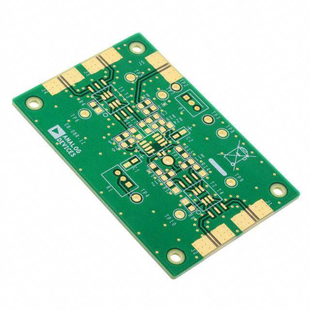
JuFN IS n 678 L55 , 211 21 01R 0 3e v 2 L1 VCC R21 .00 +Vs C1001 + BEAD C1002 C3 100nF 200Ω/DNP GND 4.7µF 1.0µF C2 1k/DRN1P9 C11 100nF DNP R17 R18 TP1 R26 DNP 200Ω C9 50Ω TEST POINT 100nF R20 C10 200Ω/DNP DNP 6 5 4 3 1 1 1 1 U1 Cterm1 D + m D IN C1µ1F ADT2-1T RRD01NPR503Ω2.2pF RR5602Ω00Ω 12 FVbi-+GN Vs Vc GNVNoC+ 1112 1Cµ7F 8R59Ω R01Ω1 R02Ω4 R351.35RΩ28 ADT1-1WT 1Cµ8F OUT DNP R4 R70Ω 34 Vi+ NC 910 C6 R10 R12 R25 R351.450ΩΩ/DNP R0Ω27 Fb- Vo- R0Ω23 R2 50Ω R8200Ω GND Vs+ PD GND 1µF 85Ω 0Ω 0Ω DNP Cterm2 ISL55210, 2.2pF 5 6 7 8 ISL55211 C4 R15 50Ω C5 TP2 DIFPROBE 100nF R16 100nF 50Ω 1 5 PD NC VCC 2 R22 A 50Ω 3 4 GND Y 74AHC1G04 P a g e FIGURE 38. SCHEMATIC FOR ISL55210, ISL55211 SINGLE INPUT TRANSFORMER EVM REV. C 1 7 o f 1 9
ISL55210 About Intersil Intersil Corporation is a leader in the design and manufacture of high-performance analog, mixed-signal and power management semiconductors. The company's products address some of the largest markets within the industrial and infrastructure, personal computing and high-end consumer markets. For more information about Intersil, visit our website at www.intersil.com. For the most updated datasheet, application notes, related documentation and related parts, please see the respective product information page found at www.intersil.com. You may report errors or suggestions for improving this datasheet by visiting www.intersil.com/en/support/ask-an-expert.html. Reliability reports are also available from our website at http://www.intersil.com/en/support/qualandreliability.html#reliability © Copyright Intersil Americas LLC 2011-2013. All Rights Reserved. All trademarks and registered trademarks are the property of their respective owners. For additional products, see www.intersil.com/en/products.html Intersil products are manufactured, assembled and tested utilizing ISO9001 quality systems as noted in the quality certifications found at www.intersil.com/en/support/qualandreliability.html Intersil products are sold by description only. Intersil may modify the circuit design and/or specifications of products at any time without notice, provided that such modification does not, in Intersil's sole judgment, affect the form, fit or function of the product. Accordingly, the reader is cautioned to verify that datasheets are current before placing orders. Information furnished by Intersil is believed to be accurate and reliable. However, no responsibility is assumed by Intersil or its subsidiaries for its use; nor for any infringements of patents or other rights of third parties which may result from its use. No license is granted by implication or otherwise under any patent or patent rights of Intersil or its subsidiaries. For information regarding Intersil Corporation and its products, see www.intersil.com FN7811 Rev 2.00 Page 18 of 19 Jun 6, 2013
ISL55210 Package Outline Drawing L16.3x3D 16 LEAD THIN QUAD FLAT NO-LEAD PLASTIC PACKAGE Rev 0, 3/10 4X 1.50 3.00 A 12X 0.50 6 B PIN #1 13 16 INDEX AREA 6 PIN 1 12 1 INDEX AREA 0 0 1.60 SQ 3. 9 4 (4X) 0.15 8 5 0.10 MCAB 16X 0.40±0.10 TOP VIEW 4 16X 0.23 ±0.05 BOTTOM VIEW SEE DETAIL “X” 0.10C C 0.75 ±0.05 0.08C SIDE VIEW (12X 0.50) (2.80 TYP)( 1.60) (16X 0.23) C 0 . 2 REF 5 (16X 0.60) 0 . 02 NOM. 0 . 05 MAX. TYPICAL RECOMMENDED LAND PATTERN DETAIL "X" NOTES: 1. Dimensions are in millimeters. Dimensions in ( ) for Reference Only. 2. Dimensioning and tolerancing conform to ASME Y14.5m-1994. 3. Unless otherwise specified, tolerance : Decimal ± 0.05 4. Dimension applies to the metallized terminal and is measured between 0.15mm and 0.25mm from the terminal tip. 5. Tiebar shown (if present) is a non-functional feature. 6. The configuration of the pin #1 identifier is optional, but must be located within the zone indicated. The pin #1 identifier may be either a mold or mark feature. 7. JEDEC reference drawing: MO-220 WEED. FN7811 Rev 2.00 Page 19 of 19 Jun 6, 2013
Mouser Electronics Authorized Distributor Click to View Pricing, Inventory, Delivery & Lifecycle Information: R enesas Electronics: ISLA214P50-55210EV1Z ISL55210IRTZ-EVALZ