ICGOO在线商城 > 集成电路(IC) > 线性 - 放大器 - 仪表,运算放大器,缓冲器放大器 > ISL28134IBZ-T7A
 Datasheet下载
- 型号: ISL28134IBZ-T7A
- 制造商: Intersil
- 库位|库存: xxxx|xxxx
- 要求:
| 数量阶梯 | 香港交货 | 国内含税 |
| +xxxx | $xxxx | ¥xxxx |
查看当月历史价格
查看今年历史价格
ISL28134IBZ-T7A产品简介:
ICGOO电子元器件商城为您提供ISL28134IBZ-T7A由Intersil设计生产,在icgoo商城现货销售,并且可以通过原厂、代理商等渠道进行代购。 ISL28134IBZ-T7A价格参考。IntersilISL28134IBZ-T7A封装/规格:线性 - 放大器 - 仪表,运算放大器,缓冲器放大器, 零漂移 放大器 1 电路 满摆幅 8-SOIC。您可以下载ISL28134IBZ-T7A参考资料、Datasheet数据手册功能说明书,资料中有ISL28134IBZ-T7A 详细功能的应用电路图电压和使用方法及教程。
ISL28134IBZ-T7A 是瑞萨电子(Renesas Electronics America Inc.)生产的一款高精度、低噪声、低输入偏置电流的双通道运算放大器,属于线性放大器中的精密运算放大器类别。其主要应用场景包括:

1. 传感器信号调理:适用于压力、温度、称重等传感器的微弱信号放大,得益于其低噪声和高精度特性。

2. 工业自动化与控制系统:用于工业仪表、PLC(可编程逻辑控制器)中的模拟信号处理与放大。

3. 医疗设备:如心电图仪、血糖仪等便携式或精密医疗设备中的信号采集与处理。

4. 测试与测量设备:用于万用表、示波器、信号发生器等仪器中的精密信号放大和缓冲。

5. 音频与模拟电路设计:在高保真音频设备中用于前置放大或模拟信号处理。

6. 电池供电设备:该器件具有低功耗特性,适合用于便携式或低功耗系统中。

该运放采用8引脚TDFN封装,易于集成于高密度PCB设计中,具备良好的温度稳定性和长期可靠性,适用于对精度和稳定性要求较高的场合。
| 参数 | 数值 |
| -3db带宽 | - |
| 产品目录 | 集成电路 (IC)半导体 |
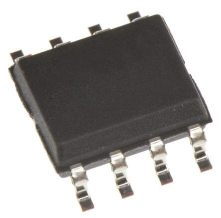
| 描述 | IC OPAMP CHOPPER 3.5MHZ 8SOIC精密放大器 ISL28134IBZ 5V ULTRA LW NOISE RAIL |
| 产品分类 | Linear - Amplifiers - Instrumentation, OP Amps, Buffer Amps集成电路 - IC |
| 品牌 | Intersil |
| 产品手册 | |
| 产品图片 |
|
| rohs | 符合RoHS无铅 / 符合限制有害物质指令(RoHS)规范要求 |
| 产品系列 | 放大器 IC,精密放大器,Intersil ISL28134IBZ-T7A- |
| 数据手册 | |
| 产品型号 | ISL28134IBZ-T7A |
| PCN组件/产地 | |
| 产品培训模块 | http://www.digikey.cn/PTM/IndividualPTM.page?site=cn&lang=zhs&ptm=25968 |
| 产品种类 | 精密放大器 |
| 供应商器件封装 | 8-SOIC |
| 共模抑制比—最小值 | 135 dB |
| 其它名称 | ISL28134IBZ-T7ATR |
| 包装 | 带卷 (TR) |
| 压摆率 | 1.5 V/µs |
| 可用增益调整 | 174 dB |
| 商标 | Intersil |
| 增益带宽生成 | 3.5 MHz |
| 增益带宽积 | 3.5MHz |
| 安装类型 | 表面贴装 |
| 安装风格 | SMD/SMT |
| 封装 | Reel |
| 封装/外壳 | 8-SOIC(0.154",3.90mm 宽) |
| 封装/箱体 | SOIC-8 |
| 工作温度 | -40°C ~ 85°C |
| 工作电源电压 | 2.25 V to 6 V |
| 工厂包装数量 | 250 |
| 放大器类型 | 断路器(零漂移) |
| 最大双重电源电压 | +/- 3 V |
| 最大工作温度 | + 85 C |
| 最小双重电源电压 | 1.125 V |
| 最小工作温度 | - 40 C |
| 标准包装 | 250 |
| 电压-电源,单/双 (±) | 2.25 V ~ 6 V, ±1.125 V ~ 3 V |
| 电压-输入失调 | 0.2µV |
| 电压增益dB | 174 dB |
| 电流-电源 | 675µA |
| 电流-输入偏置 | 120pA |
| 电流-输出/通道 | 65mA |
| 电源电压-最大 | 6 V |
| 电源电压-最小 | 2.25 V |
| 电源电流 | 675 uA |
| 电源类型 | Single, Dual |
| 电路数 | 1 |
| 系列 | ISL28134 |
| 输入偏压电流—最大 | 300 pA |
| 输入补偿电压 | 3.4 uV |
| 输出电流 | 65 mA |
| 输出类型 | 满摆幅 |
| 通道数量 | 1 Channel |


PDF Datasheet 数据手册内容提取
DATASHEET ISL28134 FN6957 5V Ultra Low Noise, Zero Drift Rail-to-Rail Precision Op Amp Rev 6.00 October 14, 2014 The ISL28134 is a single, chopper-stabilized zero drift Features operational amplifier optimized for single and dual supply operation from 2.25V to 6.0V and ±1.125V and ±3.0V. The • Rail-to-rail inputs and outputs ISL28134 uses auto-correction circuitry to provide very low - CMRR at VCM = 0.1V beyond VS. . . . . . . . . . . . . 135dB, typ input offset voltage, drift and a reduction of the 1/f noise - VOH and VOL . . . . . . . . . . . . . . . . . . . . . . .10mV from VS, typ corner below 0.1Hz. The ISL28134 achieves ultra low offset • No 1/f noise corner down to 0.1Hz voltage, offset temperature drift, wide gain bandwidth and rail- to-rail input/output swing while minimizing power - Input noise voltage . . . . . . . . . . . . . . . . .10nV/Hz at 1kHz consumption. - 0.1Hz to 10Hz noise voltage. . . . . . . . . . . . . . . . . 250nVP-P The ISL28134 is ideal for amplifying the sensor signals of • Low offset voltage . . . . . . . . . . . . . . . . . . . . . . . . . . 2.5µV, Max analog front-ends that include pressure, temperature, medical, • Superb offset drift . . . . . . . . . . . . . . . . . . . . . . . 15nV/°C, Max strain gauge and inertial sensors down to the µV levels. • Single supply . . . . . . . . . . . . . . . . . . . . . . . . . . . .2.25V to 6.0V The ISL28134 can be used over standard amplifiers with high stability across the industrial temperature range of -40°C to • Dual supply . . . . . . . . . . . . . . . . . . . . . . . . . ±1.125V to ±3.0V +85°C and the full industrial temperature range of -40°C to • Low ICC . . . . . . . . . . . . . . . . . . . . . . . . . . . . . . . . . . . 675µA, typ +125°C. The ISL28134 is available in an industry standard • Wide bandwidth. . . . . . . . . . . . . . . . . . . . . . . . . . . . . . . 3.5MHz pinout SOIC and SOT-23 packages. • Operating temperature range Applications - Industrial. . . . . . . . . . . . . . . . . . . . . . . . . . . .-40°C to +85°C • Medical instrumentation - Full industrial . . . . . . . . . . . . . . . . . . . . . . .-40°C to +125°C • Sensor gain amps • Packaging • Precision low drift, low frequency ADC drivers - Single: SOIC, SOT-23 • Precision voltage reference buffers Related Literature • Thermopile, thermocouple, and other temperature sensors •AN1641, “ISL28134SOICEVAL1Z Evaluation Board User’s front-end amplifiers Guide” • Inertial sensors •AN1560, “Making Accurate Voltage Noise and Current Noise • Process control systems Measurements on Operational Amplifiers Down to 0.1Hz” • Weight scales and strain gauge sensors 1600 1400 Vs = ±2.5V +5 ISL28134 ISL26102 FIERS 1200 NVT C ==M -2 4=70 90°6CV to +125°C LI 350Ω ISL22316 +- 50Ω 24-BIT ADC F AMP 1080000 50kΩ R O 350Ω 350Ω DCP - 50kΩ 50Ω IS5LV2 1V0R1E0F NUMBE 460000 + 200 ISL28134 0 -2.5 -2.0 -1.5 -1.0 -0.5 0 0.5 1.0 1.5 2.0 2.5 FIGURE 1. PRECISION WEIGH SCALE / STRAIN GAUGE FIGURE 2. VOS HISTOGRAM VS = 5V FN6957 Rev 6.00 Page 1 of 25 October 14, 2014
ISL28134 Pin Configurations ISL28134 ISL28134 (5 LD SOT-23) (8 LD SOIC) TOP VIEW TOP VIEW OUT 1 5 V+ NC 1 8 NC V- 2 + - IN- 2 - + 7 V+ IN+ 3 4 IN- IN+ 3 6 OUT V- 4 5 NC Pin Descriptions ISL28134 ISL28134 PIN (8 Ld SOIC) (5 Ld SOT-23) NAME FUNCTION EQUIVALENT CIRCUIT 2 4 IN- Inverting input (See Circuit 1) 3 3 IN+ Non-inverting input V+ - + - IN+ + IN- CLOCK GEN + DRIVERS V- Circuit 1 4 2 V- Negative supply 6 1 OUT Output V+ OUT V- Circuit 2 7 5 V+ Positive supply 1, 5, 8 - NC No Connect Pin is floating. No connection made to IC. FN6957 Rev 6.00 Page 2 of 25 October 14, 2014
ISL28134 Ordering Information PART NUMBER PART TEMP RANGE PACKAGE PKG. (Note4) MARKING (°C) (Pb-Free) DWG. # ISL28134IBZ (Notes1, 3) 28134 IBZ -40°C to +85°C 8 Ld SOIC M8.15E ISL28134FHZ-T7 (Notes2, 3) BEEA (Note5) -40°C to +125°C 5 Ld SOT-23 P5.064A ISL28134FHZ-T7A (Notes2, 3) BEEA (Note5) -40°C to +125°C 5 Ld SOT-23 P5.064A ISL28134ISENSEV1Z Evaluation Board ISL28134SOICEVAL1Z Evaluation Board NOTES: 1. Add “-T*” suffix for tape and reel. Please refer to TB347 for details on reel specifications. 2. Please refer to TB347 for details on reel specifications. 3. These Intersil Pb-free plastic packaged products employ special Pb-free material sets, molding compounds/die attach materials, and 100% matte tin plate plus anneal (e3 termination finish, which is RoHS compliant and compatible with both SnPb and Pb-free soldering operations). Intersil Pb-free products are MSL classified at Pb-free peak reflow temperatures that meet or exceed the Pb-free requirements of IPC/JEDEC J STD-020. 4. For Moisture Sensitivity Level (MSL), please see device information page for ISL28134. For more information on MSL please see techbrief TB363. 5. The part marking is located on the bottom of the part. FN6957 Rev 6.00 Page 3 of 25 October 14, 2014
ISL28134 Absolute Maximum Ratings Thermal Information Supply Voltage V+ to V- . . . . . . . . . . . . . . . . . . . . . . . . . . . . . . . . . . . . . . .6.5V Thermal Resistance (Typical) JA (°C/W) JC (°C/W) Voltage VIN to GND. . . . . . . . . . . . . . . . . . . . . . . . (V- - 0.3V) to (V+ + 0.3V) V 5 Ld SOT-23 (Notes6, 7) . . . . . . . . . . . . . . . 225 116 Input Differential Voltage . . . . . . . . . . . . . . . . . . . . . . . . . . . . . . . . . . . . 6.5V 8 Ld SOIC (Notes6, 7) . . . . . . . . . . . . . . . . . 125 77.2 Input Current . . . . . . . . . . . . . . . . . . . . . . . . . . . . . . . . . . . . . . . . . . . . . 20mA Maximum Storage Temperature Range . . . . . . . . . . . . . .-65°C to +150°C Voltage VOUT to GND (10s) . . . . . . . . . . . . . . . . . . . . . . . . . . . . . . .(V+) or (V-) Pb-Free Reflow Profile . . . . . . . . . . . . . . . . . . . . . . . . . . . . . . . . . . see TB493 dv/dt Supply Slew Rate. . . . . . . . . . . . . . . . . . . . . . . . . . . . . . . . . . .100V/µs ESD Rating Operating Conditions Human Body Model (Tested per JED22-A114F). . . . . . . . . . . . . . . . . 4kV Machine Model (Tested per JED22-A115B). . . . . . . . . . . . . . . . . . . .300V Ambient Operating Temperature Range Charged Device Model (Tested per JED22-C110D) . . . . . . . . . . . . . . 2kV Industrial Grade Package . . . . . . . . . . . . . . . . . . . . . . . . -40°C to +85°C Latch-up (Passed Per JESD78B). . . . . . . . . . . . . . . . . . . . . . . . . . . . +125°C Full Industrial Grade Package. . . . . . . . . . . . . . . . . . . . .-40°C to +125°C Operating Voltage Range. . . . . . . . . . . . . . . . .2.25V (±1.125V) to 6V (±3V) CAUTION: Do not operate at or near the maximum ratings listed for extended periods of time. Exposure to such conditions may adversely impact product reliability and result in failures not covered by warranty. NOTES: 6. JA is measured with the component mounted on a high effective thermal conductivity test board in free air. See Tech Brief TB379 for details. 7. For JC, the “case temp” location is taken at the package top center. Electrical Specifications VS = 5V, VCM = 2.5V, TA = +25°C, unless otherwise specified. Boldface limits apply across the specified operating temperature range. MIN MAX PARAMETER DESCRIPTION TEST CONDITIONS (Note8) TYP (Note8) UNITS DC SPECIFICATIONS VOS Input Offset Voltage -2.5 -0.2 2.5 µV TA = -40°C to +85°C -3.4 - 3.4 µV TA = -40°C to +125°C -4 - -4 µV TCVOS Input Offset Voltage Temperature TA = -40°C to +125°C -15 -0.5 15 nV/°C Coefficient IB Input Bias Current -300 ±120 300 pA TA = -40°C to +85°C -300 - 300 pA TA = -40°C to +125°C -550 - 550 pA TCIB Input Bias Current Temperature TA = -40°C to +85°C - ±1.4 - pA/°C Coefficient TA = -40°C to +125°C - ±2 - pA/°C IOS Input Offset Current -600 ±240 600 pA TA = -40°C to +85°C -600 - 600 pA TA = -40°C to +125°C -750 - 750 pA TCIOS Input Offset Current Temperature Coefficient TA = -40°C to +85°C - ±2.8 - pA/°C TA = -40°C to +125°C - ±4 - pA/°C Common Mode Input V+ = 5.0V, V- = 0V -0.1 - 5.1 V Voltage Range Guaranteed by CMRR CMRR Common Mode Rejection Ratio VCM = -0.1V to 5.1V 120 135 - dB VCM = -0.1V to 5.1V 115 - - dB PSRR Power Supply Rejection Ratio VS = 2.25V to 6.0V 120 135 - dB VS = 2.25V to 6.0V 120 - - dB VS Supply Voltage (V+ to V-) Guaranteed by PSRR 2.25 - 6.0 V FN6957 Rev 6.00 Page 4 of 25 October 14, 2014
ISL28134 Electrical Specifications VS = 5V, VCM = 2.5V, TA = +25°C, unless otherwise specified. Boldface limits apply across the specified operating temperature range. (Continued) MIN MAX PARAMETER DESCRIPTION TEST CONDITIONS (Note8) TYP (Note8) UNITS IS Supply Current Per Amplifier RL = OPEN - 675 900 µA RL = OPEN - - 1075 µA TA = -40°C to +85°C RL = OPEN - - 1150 µA TA = -40°C to +125°C ISC Short Circuit Output Source Current RL = Short to V- - 65 - mA Short Circuit Output Sink Current RL = Short to V+ - -65 - mA VOH Output Voltage Swing, HIGH RL = 10kΩto VCM 15 10 - mV From VOUT to V+ RL = 10kΩto VCM 15 - - mV VOL Output Voltage Swing, LOW RL = 10kΩto VCM - 10 15 mV From V- to VOUT RL = 10kΩto VCM - - 15 mV AOL Open Loop Gain RL = 1MΩ - 174 - dB AC SPECIFICATIONS CIN Input Capacitance Differential - 5.2 - pF Common Mode - 5.6 - pF eN Input Noise Voltage f = 0.1Hz to 10Hz - 250 400 nVP-P f = 10Hz - 8 - nV/Hz f = 1kHz - 10 - nV/Hz IN Input Noise Current f = 1kHz - 200 - fA/Hz GBWP Gain Bandwidth Product - 3.5 - MHz EMIRR EMI Rejection Ratio AV = +1, VIN = 200mVp-p, VCM = 0V, - 75 - dB V+=2.5V, V- = -2.5V TRANSIENT RESPONSE SR Positive Slew Rate V+ = 5V, V- = 0V, VOUT = 1V to 3V, RL = 100kΩ, - 1.5 - V/µs CL=3.7pF Negative Slew Rate - 1.0 - V/µs tr, tf, Small Signal Rise Time, tr 10% to 90% V+ = 5V, V- = 0V, VOUT = 0.1VP-P, RF= 0Ω, - 0.07 - µs RL = 100kΩ, CL=3.7pF Fall Time, tf 10% to 90% - 0.17 - µs tr, tf Large Signal Rise Time, tr 10% to 90% V+ = 5V, V- = 0V, VOUT = 2VP-P, RF=0Ω, - 1.3 - µs RL = 100kΩ, CL=3.7pF Fall Time, tf 10% to 90% - 2.0 - µs ts Settling Time to 0.1%, 2VP-P Step AV = -1, RF = 1kΩ, CL = 3.7pF - 100 - µs trecover Output Overload Recovery Time, Recovery AV = +2, RF = 10kΩ, RL=100k, CL = 3.7pF - 3.1 - µs to 90% of Output Saturation VOS Input Offset Voltage -2.5 -0.2 2.5 µV TA = -40°C to +85°C -3.4 - 3.4 µV TA = -40°C to +125°C -4 - -4 µV TCVOS Input Offset Voltage Temperature TA = -40°C to +125°C -15 -0.5 15 nV/°C Coefficient FN6957 Rev 6.00 Page 5 of 25 October 14, 2014
ISL28134 Electrical Specifications VS = 2.5V, VCM = 1.25V, TA = +25°C, unless otherwise specified. Boldface limits apply over the specified operating temperature range. MIN MAX PARAMETER DESCRIPTION TEST CONDITIONS (Note8) TYP (Note8) UNITS DC SPECIFICATIONS IB Input Bias Current -300 ±120 300 pA TA = -40°C to +85°C -300 - 300 pA TA = -40°C to +125°C -550 - 550 pA TCIB Input Bias Current Temperature TA = -40°C to +85°C - ±1.4 - pA/°C Coefficient TA = -40°C to +125°C - ±2 - pA/°C IOS Input Offset Current -600 ±240 600 pA TA = -40°C to +85°C -600 - 600 pA TA = -40°C to +125°C -750 - 750 pA TCIOS Input Offset Current Temperature TA = -40°C to +85°C - ±2.8 - pA/°C Coefficient TA = -40°C to +125°C - ±4 - pA/°C Common Mode Input V+ = 2.5V, V- = 0V -0.1 - 2.6 V Voltage Range Guaranteed by CMRR CMRR Common Mode Rejection Ratio VCM = -0.1V to 2.6V 120 135 - dB VCM = -0.1V to 2.6V 115 - - dB IS Supply Current per Amplifier RL = OPEN - 715 940 µA RL = OPEN - - 1115 µA TA = -40°C to +85°C RL = OPEN - - 1190 µA TA = -40°C to +125°C ISC Short Circuit Output Source Current RL = Short to Ground - 65 - mA Short Circuit Output Sink Current RL = Short to V+ - -65 - mA VOH Output Voltage Swing, HIGH RL = 10kΩ to VCM 15 10 - mV From VOUT to V+ RL = 10kΩ to VCM 15 - - mV VOL Output Voltage Swing, LOW RL = 10kΩ to VCM - 10 15 mV From V- to VOUT RL = 10kΩ to VCM - - 15 mV AC SPECIFICATIONS CIN Input Capacitance Differential - 5.2 - pF Common Mode - 5.6 - pF eN Input Noise Voltage f = 0.1Hz to 10Hz - 250 400 nVP-P f = 10Hz - 8 - nV/Hz f = 1kHz - 10 - nV/Hz IN Input Noise Current f = 1kHz - 200 - fA/Hz GBWP Gain Bandwidth Product - 3.5 - MHz FN6957 Rev 6.00 Page 6 of 25 October 14, 2014
ISL28134 Electrical Specifications VS = 2.5V, VCM = 1.25V, TA = +25°C, unless otherwise specified. Boldface limits apply over the specified operating temperature range. (Continued) MIN MAX PARAMETER DESCRIPTION TEST CONDITIONS (Note8) TYP (Note8) UNITS TRANSIENT RESPONSE SR Positive Slew Rate V+ = 2.5V, V- = 0V, VOUT = 0.25V to 2.25V, - 1.5 - V/µs RL= 100kΩ, CL=3.7pF Negative Slew Rate - 1.0 - V/µs tr, tf, Small Signal Rise Time, tr 10% to 90% V+ = 2.5V, V- = 0V, VOUT = 0.1VP-P, - 0.07 - µs RF= 0Ω, RL = 100kΩ, CL=3.7pF Fall Time, tf 10% to 90% - 0.17 - µs tr, tf Large Signal Rise Time, tr 10% to 90% V+ = 2.5V, V- = 0V, VOUT = 2VP-P, RF=0Ω, - 1.3 - µs RL= 100kΩ, CL=3.7pF Fall Time, tf 10% to 90% - 2.0 - µs ts Settling Time to 0.1%, 2VP-P Step AV = -1, RF = 1kΩ, CL = 3.7pF - 100 - µs trecover Output Overload Recovery Time, Recovery AV = +2, RF = 10kΩ, RL=100k, - 1.5 - µs to 90% of Output Saturation CL = 3.7pF NOTE: 8. Compliance to datasheet limits is assured by one or more methods: production test, characterization and/or design. Typical Performance Curves TA = +25°C, VCM = 0V Unless otherwise specified. 2.0 2.0 1.5 1.5 GE (µV) 01..50 GE (µV) 01..50 OLTA 0 OLTA 0 OFFSET V --10..05 OFFSET V --10..05 VS = ±2.5V -1.5 VS = ±1.125V -1.5 VCM = 0V VCM = 0V -2.0 -2.0 -50 -20 10 40 70 100 130 -50 -20 10 40 70 100 130 TEMPERATURE (°C) TEMPERATURE (°C) FIGURE 3. VOS vs TEMPERATURE, VS = ±2.5V FIGURE 4. VOS vs TEMPERATURE, VS = ±1.125V 1600 160 Vs = ±2.5V 1400 Vs = ±2.5V 140 VCM = 0V VCM = 0V T = -40°C to +125°C ERS 1200 NT == -24709°6C to +125°C ERS 120 N = 480 FI FI LI 1000 LI 100 P P M M F A 800 F A 80 O O ER 600 ER 60 B B M M NU 400 NU 40 200 20 0 0 -2.5 -2.0 -1.5 -1.0 -0.5 0 0.5 1.0 1.5 2.0 2.5 -10 -8 -6 -4 -2 0 2 4 6 8 10 VOS (µV) TCVOS (nV/°C) FIGURE 5. VOS HISTOGRAM VS = 5V FIGURE 6. TCVOS HISTOGRAM VS = 5V FN6957 Rev 6.00 Page 7 of 25 October 14, 2014
ISL28134 Typical Performance Curves TA = +25°C, VCM = 0V Unless otherwise specified. (Continued) 1400 120 1200 VVsC M= ±=1 0.2V5V 100 VVsC M= ±=1 0.2V5V S T = -40°C to +125°C S T = -40°C to +125°C ER 1000 N = 2325 ER N = 310 FI FI 80 LI LI MP 800 MP A A F F 60 O O R 600 R E E B B 40 M 400 M U U N N 20 200 0 0 -2.5 -2.0 -1.5 -1.0 -0.5 0 0.5 1.0 1.5 2.0 2.5 -10 -8 -6 -4 -2 0 2 4 6 8 10 VOS (µV) TCVOS (nV/°C) FIGURE 7. VOS HISTOGRAM VS = 2.5V FIGURE 8. TCVOS HISTOGRAM VS = 2.5V 4 4 3 3 V) 2 V) 2 µ µ E ( 1 Vs = ±2.5V E ( 1 G G A A T T OL 0 OL 0 V V T T E -1 E -1 S S F F F F O -2 O -2 Vs = ±1.125V -3 -3 -4 -4 -3.2 -2.4 -1.6 -0.8 0 0.8 1.6 2.4 3.2 1.0 1.5 2.0 2.5 3.0 3.5 COMMON MODE VOLTAGE (V) SUPPLY VOLTAGE (V) FIGURE 9. VOS vs VCM FIGURE 10. VOS vs SUPPLY VOLTAGE 500 600 400 IB+ Vs = ±2.5V 500 A) 300 IB+ Vs = ±1.125V pA) T (p 200 NT ( 400 N E E 100 R R R 300 S CUR 0.00 IB- Vs = ±2.5V IB- Vs = ±1.125V ET CU 200 Vs = ±2.5V A -100 S BI FF T -200 O U T 100 P U IN -300 NP I -100 -400 Vs = ±1.125V -500 -200 -3 -2 -1 0 1 2 3 -3 -2 -1 0 1 2 3 COMMON MODE VOLTAGE (V) COMMON MODE VOLTAGE (V) FIGURE 11. IB vs VCM FIGURE 12. IOS vs VCM FN6957 Rev 6.00 Page 8 of 25 October 14, 2014
ISL28134 Typical Performance Curves TA = +25°C, VCM = 0V Unless otherwise specified. (Continued) 350 350 300 IB+ 300 NT (pA) 220500 IB+VS = ±2.5V ENT (pA) 220500 VS = ±2.5V RE VS = ±1.125V RR 150 R 150 U BIAS CU 100 VIBS- = ±1.125V VIBS- = ±2.5V FFSET C 15000 VS = ±1.125V T 50 O U T 0 P U N 0 P I N -50 I -50 -100 -100 -150 -40 -20 0 20 40 60 80 100 120 140 -40 -20 0 20 40 60 80 100 120 140 TEMPERATURE (°C) TEMPERATURE (°C) FIGURE 13. IB vs TEMPERATURE FIGURE 14. IOS vs TEMPERATURE 160 1000 T = +125°C 150 PSRR 900 T = +85°C A) µ R (dB) 140 ENT ( 800 T = +25°C R R S 130 R P U R/ C R CMRR Y 700 CM 120 PPL U PSRR CMRR S 600 110 T = -40°C VS = ±1.125V TO ±3V VS =±2.5V VCM = 0V VCM = -2.6V TO +2.6V 100 500 -40 -20 0 20 40 60 80 100 120 140 2.0 3.0 4.0 5.0 6.0 TEMPERATURE (°C) SUPPLY VOLTAGE (V) FIGURE 15. CMRR and PSRR vs TEMPERATURE FIGURE 16. SUPPLY CURRENT vs SUPPLY VOLTAGE 1000 1000 VS = ±2.5V VS = ±2.5V T = -40°C to +125°C T = -40°C to +125°C mV) mV) V+ RAIL ( 100 V- RAIL ( 100 M M O O R R F F E E G 10 G 10 A A T T L L O O V V 1 1 0.01 0.1 1.0 10 100 0.01 0.1 1.0 10 100 LOAD CURRENT (mA) LOAD CURRENT (mA) FIGURE 17. OUTPUT HIGH OVERHEAD VOLTAGE vs LOAD CURRENT FIGURE 18. OUTPUT LOW OVERHEAD VOLTAGE vs LOAD CURRENT FN6957 Rev 6.00 Page 9 of 25 October 14, 2014
ISL28134 Typical Performance Curves TA = +25°C, VCM = 0V Unless otherwise specified. (Continued) 1.0 1.0 V) VRSL == O±2U.5TV to GND RL = 1kΩ V) VRSL == O±2U.5TV to GND RL = 1kΩ m m AIL ( 0.1 AIL ( 0.1 R R V+ V- M M O O R R F F E E G 0.01 G 0.01 A A LT LT O O V RL = 12.5kΩ V RL = 12.5kΩ 0.001 0.001 -40 -20 0 20 40 60 80 100 120 140 -40 -20 0 20 40 60 80 100 120 140 TEMPERATURE (°C) TEMPERATURE (°C) FIGURE 19. VOH vs TEMPERATURE FIGURE 20. VOL vs TEMPERATURE 100 300 200 z) V) 100 H n V√ E ( E (n 10 TAG 0.00 S L OI O N V -100 VS = ±2.5V -200 AV = 10,000 Rg = 10, Rf = 100k 1 -300 0.001 0.01 0.1 1 10 0 1 2 3 4 5 6 7 8 9 10 FREQUENCY (Hz) TIME (s) FIGURE 21. INPUT NOISE VOLTAGE DENSITY vs FREQUENCY FIGURE 22. INPUT NOISE VOLTAGE 0.1Hz TO 10Hz 1000 140 CIN+ = 0pF VAVS == 1±2.5V 120 GAIN PHASE z) RS = 5MΩ 100 A/√H E (°) T NOISE (f 100 dB) / PHAS 6800 URREN CIN+ =100pF GAIN ( 40 C 20 VS = ±2.5V 0 RL = 10MΩ SIMULATION 10 -20 0.1 1 10 100 1000 10k 100k 0.1 1 10 100 1k 10k 100k 1M 10M 100M FREQUENCY (Hz) FREQUENCY (Hz) FIGURE 23. INPUT NOISE CURRENT DENSITY vs FREQUENCY FIGURE 24. OPEN LOOP GAIN AND PHASE, RL = 10M FN6957 Rev 6.00 Page 10 of 25 October 14, 2014
ISL28134 Typical Performance Curves TA = +25°C, VCM = 0V Unless otherwise specified. (Continued) 140 90 GAIN PHASE 80 AV = 10,000 Rg = 10, Rf = 100k 120 70 100 60 AV = 1000 Rg = 100, Rf = 100k SE (°) 80 4500 AV = 100 VS = ± 2.5V B) / PHA 60 AIN (dB) 2300 AV = 10 Rg = 1k, Rf = 100k VCROLL U==T 31 =.07 01pk0FmVP-P AIN (d 40 G 100 AV = 1 Rg = 10k, Rf = 100k G 20 VS = ±2.5V -10 Rg = OPEN, Rf = 0 0 RL = 10kΩ -20 SIMULATION -30 -20 -40 0.1 1 10 100 1k 10k 100k 1M 10M 100M 10 100 1k 10k 100k 1M 10M 100M FREQUENCY (Hz) FREQUENCY (Hz) FIGURE 25. OPEN LOOP GAIN AND PHASE, RL = 10k FIGURE 26. FREQUENCY RESPONSE vs CLOSED LOOP GAIN 2 4 1 2 0 RL > 10kΩ 1 0 B) -2 B) -2 GAIN (d --43 RL > 10kΩ GAIN (d -4 RL = 1kΩ RL = 1kΩ -5 -6 --67 CVAVLS === 31±.V 71p.2F5V -8 CVAVLS === 31±.V 72p.5FV VOUT = 10mVP-P VOUT = 10mVP-P -8 -10 10k 100k 1M 10M 100k 1M 10M 100M FREQUENCY (Hz) FREQUENCY (Hz) FIGURE 27. GAIN vs FREQUENCY vs RL, VS = 2.5V FIGURE 28. GAIN vs FREQUENCY vs RL, VS = 5.0V 15 2 VS = ± 2.5V Rg = 100k, Rf = 100k AV = 2V 0 10 RL = 100k B) VOUT = 10mVP-P d N ( Rg = 10k, Rf = 10k -2 GAI 5 B) ALIZED 0 Rg = 1k, Rf = 1k GAIN (d -4 15V0P0-mPVP-P M OR -6 250mVP-P N -5 -8 VAVS == 1±V 2.5V 100mVP-P RL = OPEN 10mVP-P CL = 3.7pF -10 -10 100 1k 10k 100k 1M 10M 100M 10 100 1k 10k 100k 1M 10M 100M FREQUENCY (Hz) FREQUENCY (Hz) FIGURE 29. GAIN vs FREQUENCY vs FEEDBACK RESISTOR VALUES FIGURE 30. GAIN vs FREQUENCY vs VOUT Rf/Rg FN6957 Rev 6.00 Page 11 of 25 October 14, 2014
ISL28134 Typical Performance Curves TA = +25°C, VCM = 0V Unless otherwise specified. (Continued) 12 2 824pF 10 VAVS == 1±V 2.5V 1nF ±1.5V ±3.0V 0 RL = 100k 474pF 8 VOUT = 10mVP-P 6 -2 104pF dB) 4 dB) N ( N ( -4 ±0.8V AI 2 AI G G 0 51pF -6 VOUT = 10mVP-P -2 AV = 1V -4 3.7pF -8 RL = 100k CL = 3.7pF -6 -10 10k 100k 1M 10M 100M 1M 10M FREQUENCY (Hz) FREQUENCY (Hz) FIGURE 31. GAIN vs FREQUENCY vs CL FIGURE 32. GAIN vs FREQUENCY vs SUPPLY VOLTAGE 120 100 B) 80 d + ( R IN 60 R MI E 40 20 0 10 100 1k 10k FREQUENCY (MHz) FIGURE 33. EMIRR AT IN+ PIN vs FREQUENCY 160 160 140 140 120 120 dB) 100 dB) 100 R ( R ( R R M 80 M 80 C C 60 60 VS = ±2.5V VS = ±1.25V 40 VCM = 0V 40 VCM = 0V SIMULATION SIMULATION 20 20 1m 0.1 10 1k 100k 10M 1m 0.1 10 1k 100k 10M FREQUENCY (Hz) FREQUENCY (Hz) FIGURE 34. CMRR vs FREQUENCY, VS = 5V FIGURE 35. CMRR vs FREQUENCY, VS = 2.5V FN6957 Rev 6.00 Page 12 of 25 October 14, 2014
ISL28134 Typical Performance Curves TA = +25°C, VCM = 0V Unless otherwise specified. (Continued) 140 120 120 -PSRR 100 +PSRR 100 80 -PSRR +PSRR B) 80 B) d d N ( N ( 60 GAI 60 GAI 40 40 VS = ± 2.5VDC VS = ± 1.25VDC AV = 1V AV = 1V 20 RL = 100k 20 RL = 100k VIN = 1VP-P VIN = 1VP-P 0 0 10 100 1k 10k 100k 1M 10M 10 100 1k 10k 100k 1M 10M FREQUENCY (Hz) FREQUENCY (Hz) FIGURE 36. PSRR vs FREQUENCY, VS = 5V FIGURE 37. PSRR vs FREQUENCY, VS = 2.5V 4 4.5 3 4.0 2 3.5 INPUT 3.0 VOLTAGE (V) -101 VS = ±2.5V VOLTAGE (V) 22..05 OUTPUT AV = 1V 1.5 -2 RL = 1MΩ VS = 5VDC VIN = -3V TO 3V 1.0 AV = 1V -3 RL = 100k 0.5 VIN = 1V TO 4V -4 0.0 0 5 10 15 20 0 5 10 15 20 TIME (ms) TIME (µs) FIGURE 38. NO PHASE INVERSION FIGURE 39. LARGE SIGNAL STEP RESPONSE (3V) 1.2 0.10 1.0 0.08 0.8 V) INPUT V) 0.06 OUTPUT E ( E ( AG 0.6 AG 0.04 LT LT INPUT O O V 0.4 OUTPUT V 0.02 0.2 VVARVISLN === = 115 0V0V.01DkVC TO 1.1V -0.020 VVARVSILN == == ±1 102V0V.05 kTVOD C0.1V 0 -0.04 0 2 4 6 8 10 0 2 4 6 8 10 TIME (µs) TIME (µs) FIGURE 40. LARGE SIGNAL STEP RESPONSE (1V) FIGURE 41. SMALL SIGNAL STEP RESPONSE (100mV) FN6957 Rev 6.00 Page 13 of 25 October 14, 2014
ISL28134 Typical Performance Curves TA = +25°C, VCM = 0V Unless otherwise specified. (Continued) 60 55 55 50 50 - OS 45 - OS %) 45 %) 40 OVERSHOOT ( 334050 +OS OVERSHOOT ( 233505 +OS 25 20 VAVS == 1±V2.5V 20 VAVS == ±11V.25V 15 VROL U=T 1 =0 01k00mVp-p 15 VROL U=T 1 =0 01k00mVp-p 10 10 10 100 1000 10 100 1000 LOAD CAPACITANCE (pF) LOAD CAPACITANCE (pF) FIGURE 42. SMALL SIGNAL OVERSHOOT vs LOAD CAPACITANCE, FIGURE 43. SMALL SIGNAL OVERSHOOT vs LOAD CAPACITANCE, VS = ±2.5V VS = ±1.25V Applications Information 0.01µF or larger high frequency decoupling capacitor is placed across the power supply pins of the IC to maintain high performance Functional Description of the amplifier. The ISL28134 is a single 5V rail-to-rail input/output amplifier Rail-to-rail Input and Output (RRIO) that operates on a single or dual supply. The ISL28134 uses a Unlike some amplifiers whose inputs may not be taken to the power proprietary chopper-stabilized technique that combines a 3.5MHz supply rails or whose outputs may not drive to the supply rails, the main amplifier with a very high open loop gain (174dB) chopper ISL28134 features rail-to-rail inputs and outputs. This allows the amplifier to achieve very low offset voltage and drift (0.2µV, amplifier inputs to have a wide common mode range (100mV 0.5nV/°C) while having a low supply current (675µA). The very low beyond supply rails) while maintaining high CMRR (135dB) and 1/f noise corner <0.1Hz and low input noise voltage (8nV/√Hz at maximizes the signal to noise ratio of the amplifier by having the 100Hz) of the amplifier makes it ideal for low frequency precision applications requiring very high gain and low noise. VOH and VOL levels be at the V+ and V- rails, respectively. Low Input Voltage Noise Performance This multi-path amplifier architecture contains a time continuous main amplifier whose input DC offset is corrected by a In precision applications, the input noise of the front end parallel-connected, high gain chopper stabilized DC correction amplifier is a critical parameter. Combined with a high DC gain to amplifier operating at 100kHz. From DC to ~10kHz, both amplify the small input signal, the input noise voltage will result amplifiers are active with the DC offset correction active with in an output error in the amplifier. A 1µVP-P input noise voltage most of the low frequency gain provided by the chopper with an amplifier gain of 10,000V/V will result in an output offset amplifier. A 10kHz crossover filter cuts off the low frequency in the range of 10mV, which can be an unacceptable error chopper amplifier path leaving the main amplifier active out to source. With only 250nVP-P at the input, along with a flat noise the -3dB frequency (3.5MHz GBWP). response down to 0.1Hz, the ISL28134 can amplify small input signals with minimal output error. The key benefits of this architecture for precision applications are rail-to-rail inputs/outputs, high open loop gain, low DC offset and The ISL28134 has the lowest input noise voltage compared to temperature drift, low 1/f noise corner and low input noise other competitor Zero Drift amplifiers with similar supply voltage. The noise is virtually flat across the frequency range currents (see Table1). The overall input referred voltage noise of from a few MHz out to 100kHz, except for the narrow noise peak an amplifier can be expressed as a sum of the input noise at the amplifier crossover frequency (10kHz). voltage, input noise current of the amplifier and the Johnson noise of the gain-setting resistors used. The product of the input Power Supply Considerations noise current and external feedback resistors along with the The ISL28134 features a wide supply voltage operating range. The Johnson noise, increases the total output voltage noise as the ISL28134 operates on single (+2.25V to +6.0V) or dual (±1.125 to value of the resistance goes up. For optimizing noise ±3.0V) supplies. Power supply voltages greater than the +6.5V performance, choose lower value feedback resistors to minimize absolute maximum (specified in the “Absolute Maximum Ratings” the effect of input noise current. Although the ISL28134 features on page4) can permanently damage the device. Performance of a very low 200fA/Hz input noise current, at source impedances the device is optimized for supply voltages greater than 2.5V. This >100kΩ, the input referred noise voltage will be dominated by makes the ISL28134 ideal for portable 3V battery applications that the input current noise. Keep source input impedances under require the precision performance. It is highly recommended that a 10kΩ for optimum performance. FN6957 Rev 6.00 Page 14 of 25 October 14, 2014
ISL28134 TABLE 1. IN+ and IN- Protection VOLTAGE NOISE AT 0.1Hz TO 10Hz PEAK-TO-PEAK The ISL28134 is capable of driving the input terminals up to and PART 100Hz VOLTAGE NOISE beyond the supply rails by about 0.5V. Back biased ESD diodes from the input pins to the V+ and V- rails will conduct current Competitor A 22nV/√Hz 600nVP-P when the input signals go more than 0.5V beyond the rail (see Competitor B 16nV/√Hz 260nVP-P Figure45). The ESD protection diodes must be current limited to 20mA or less to prevent damage of the IC. This current can be Competitor C 90nV/√Hz 1500nVP-P reduced by placing a resistor in series with the IN+ and IN- inputs ISL28134 8nV/√Hz 250nVP-P in the event the input signals go beyond the rail. High Source Impedance Applications IN- The input stage of Chopper Stabilized amplifiers do not behave - like conventional amplifier input stages. The ISL28134 uses RIN IN+ VOUT VIN + switches at the chopper amplifier input that continually ‘chops’ RL the input signal at 100kHz to reduce input offset voltage down to ESD 1µV. The dynamic behavior of these switches induces a charge DIODES V+ injection current to the input terminals of the amplifier. The V- charge injection current has a DC path to ground through the resistances seen at the input terminals of the amplifier. Higher FIGURE 45. INPUT CURRENT LIMITING input impedance cause an apparent shift in the input bias current of the amplifier. Input impedances larger than 10kΩ EMI Rejection begin to have significant increases in the bias currents. To minimize the effect of impedance on input bias currents, an Electromagnetic Interference (EMI) can be a problem in high input resistance of <10kΩ is recommended. frequency applications for precision amplifiers. The op amp pins are susceptible to EMI signals which can rectify high frequency Because the chopper amplifier has charge injection currents at inputs beyond the amplifier bandwidth and present itself as a each terminal, the input impedance should be balanced across shift in DC offset voltage. Long trace leads to op amp pins may each input (see Figure44). The input impedance of the amplifier act as an antenna for radiated RF signals, which result in a total should be matched between the IN+ and IN- terminals to conductive EMI noise into the op amp inputs. minimize total input offset current. Input offset currents show up as an additional output offset voltage, as shown in Equation1: The most susceptible pin is the non-inverting IN+ input therefore, EMI rejection (EMIR) on this pin is important for RF type VOSTOT = VOS - RF*IOS (EQ. 1) applications. The ability of the amplifier output to reject EMI is called EMI Rejection Ratio (EMIRR) and is computed as: If the offset voltage of the amplifier is negative, the input offset currents will add to the total output offset. For a 10,000V/V gain EMIRR (dB) = 20 log (VIN_PEAK/ΔVOS amplifier using 1MΩ feedback resistor, a 500pA total input offset The test circuit for measuring the DC offset of the amplifier with current will have an additional output offset voltage of 0.5mV. By an RF signal input to the IN+ pin is shown in Figure46. The keeping the input impedance low and balanced across the EMIRR performance of the ISL28134 at the IN+ pin across a amplifier inputs, the input offset current is kept below 100pA, frequency of 10MHz to 2.4GHz is plotted on Figure33. The resulting in an offset voltage 0.1mV or less. ISL28134 shows a typical EMIRR of 75dB at 1GHz. For better EMI immunity, a small RFI filter can be placed at the input to RI RF attenuate out of band signals and reduce DC offset shift from +2.5V high frequency RF signals into the IN+ pin. For example, a 15Ω and 100pF RC filter will roll off signals above 100MHz for better EMIRR performance. - RS VOUT VIN + RL +2.5V IN- Rg - -2.5V VIN = 200mVP-P IN+ VOUT + RL= 10kΩ -2.5V RF//RI = RS//Rg FIGURE 44. CIRCUIT IMPLEMENTATION FOR REDUCING INPUT BIAS CURRENTS FIGURE 46. CIRCUIT TESTING EMIRR FN6957 Rev 6.00 Page 15 of 25 October 14, 2014
ISL28134 Output Phase Reversal ISL28134 SPICE Model The Output phase reversal is the unexpected inversion of the Figure48 shows the SPICE model schematic and Figure49 shows amplifier output signal when the inputs exceed the common the net list for the SPICE model. The model is a simplified version mode input range. Since the ISL28134 is a rail-to-rail input of the actual device and simulates important AC and DC amplifier, the ISL28134 is specifically designed to prevent output parameters. The AC parameters incorporated into the model are: phase reversal within its common mode input range. In fact, the 1/f and flat band noise voltage, slew rate, CMRR, and gain and ISL28134 will not phase invert even when the input signals go phase. The DC parameters are IOS, VOS, total supply current, 0.5V beyond the supply rails (see Figure38). If input signals are output voltage swing and output current limit (65mA). The model expected to go beyond the rails, it is highly recommended to uses typical parameters given in the “Electrical Specifications” minimize the forward biased ESD diode current to prevent phase table beginning on page4. The AVOL is adjusted for 174dB with inversion by placing a resistor in series with the input. the dominant pole at 6.5mHz. The CMRR is set at 135dB, f=200Hz. The input stage models the actual device to present an High Gain, Precision DC-Coupled Amplifier accurate AC representation. The model is configured for an Precision applications that need to amplify signals in the range ambient temperature of +25°C. of a few µV require gain in the order of thousands of V/V to get a Figures50 through 63 show the characterization vs simulation good signal to the Analog to Digital Converter (ADC). This can be results for the noise voltage, open loop gain phase, closed loop achieved by using a very high gain amplifier with the appropriate gain vs frequency, CMRR, large signal 3V step response, large open loop gain and bandwidth. signal 1V step response, and output voltage swing VOH/VOL ±2.5V supplies (no phase inversion). In addition to the high gain and bandwidth, it is important that the amplifier have low VOS and temperature drift along with a LICENSE STATEMENT low input noise voltage. For example, an amplifier with 100µV offset voltage and 0.5µV/°C offset drift configured in a closed loop The information in the SPICE model is protected under United gain of 10,000V/V would produce an output error of 1V and a States copyright laws. Intersil Corporation hereby grants users of 5mV/°C temperature dependent error. Unless offset trimming and this macro-model, hereto referred to as “Licensee”, a temperature compensation techniques are used, this error makes it nonexclusive, nontransferable license to use this model, as long difficult to resolve the input voltages needed in the precision as the Licensee abides by the terms of this agreement. Before application. using this Macro-Model, the Licensee should read this license. If the Licensee does not accept these terms, permission to use the The ISL28134 features a low VOS of ±4µV max and a very stable model is not granted. 10nV/°C max temperature drift, which produces an output error of only ±40mV and a temperature error of 0.1mV/°C. With an ultra The Licensee may not sell, loan, rent, or license the low input noise of 210nVP-P (0.1Hz to 10Hz) and no 1/f corner macro-model, in whole, in part, or in modified form, to anyone frequency, the ISL28134 is capable of amplifying signals in the µV outside the Licensee’s company. The Licensee may modify the range with high accuracy. For even further DC precision, some Macro-Model to suit his/her specific applications, and the feedback filtering CF (see Figure47) to reduce the noise can be Licensee may make copies of this Macro-Model for use within implemented as a total signal stage amplifier. As a method of best their company only. practice, the ISL28134 should be impedance matched at the two This Macro-Model is provided “AS IS, WHERE IS, AND WITH NO input terminals. A balancing capacitor of the same value at the WARRANTY OF ANY KIND EITHER EXPRESSED OR IMPLIED, on-inverting terminal will result in the amplifier input impedances INCLUDING BUT NOT LIMITED TO ANY IMPLIED WARRANTIES OF tracking across frequency MERCHANTABILITY AND FITNESS FOR A PARTICULAR PURPOSE.” In no event will Intersil be liable for special, collateral, incidental, or CF consequential damages in connection with or arising out of the use of this Macro-Model. Intersil reserves the right to make 100Ω 1MΩ changes to the product and the Macro-Model without prior notice. +2.5V ACL = 10kV/V - 100Ω VOUT VIN + RL 1MΩ CF -2.5V FIGURE 47. HIGH GAIN, PRECISION DC-COUPLED AMPLIFIER FN6957 Rev 6.00 Page 16 of 25 October 14, 2014
October 14, 2014FN6957Rev 6.00 Vin+ RR2211 ++++---- EEnn En 00..22EE--66 VVOOSS1 IN+ 3MNMNCC1144HH7R7RAA..1155NN00NN00EE44LLMMVV211OOM11MSSee11FF--5566EETT47R7R..225500I0044N- 9R1R10055 81R1RII22005566ee--3310 GGAAIINN == +-G+-G22331133AA..442266 1RR4AA11 11 R1R10099DDDD002211 DXDXDXDX 151R1Ree119900 GGAAIINN == 111133..99+-G+-G6611ee--33 RR111100..6611001776DXDX1DD733VV33 ISL28134 NNCCHHAANNNNEELLMMOOSSFFEETT PPMMOOSSIISSIILL 8800 28 5 6 MM1100 MM1111 RR2222 EEOOSS PPMMOOSSIISSIILL 55ee1111 ++ DNDN DD1133 ++-- -- 11 12 0 VV99 29 0 RR2233 C4C4..ii77nn11DDeeiiff--1122 IIOOSS 00..660077 VV44 55ee1111 Vcm 224400ee--1122 RR33 7 RR44 RR77 18 Vin- 00..14 1100 1100 77..1553 R7R7..8855 GG--22AA RRAA22 11 GG--22 RR1122 11 ++ ++ GGAAIINN == 223333..442266 GGAAIINN == 111133..9966ee--33 II11 VV22 55ee--33 11ee--66 DXDX DD44 CCiinn22 CCiinn11 1100..11ee--1122 1100..11ee--1122 Differential to Single Ended 1st Gain Stage Voltage Noise Stage Input Stage Conversion Stage V+ EE22 ++--++-- GGAAIINN == 11 V++ 0 DXDX DD55 LL11 GG1111 GGAAIINN == +-G+-G668833..222255EE--33 00..660077 19VV55 7733RR44116633..0066EE66 33..CC333322EE--0099 GGAAIINN == 117777..88+-G+-G3355EE--66 2771..R1R199..551100775500EEEE----00007733 GGAAIINN+-G+-G ==77 887799..6622EE--66 1111RR33116677..8855 1100CCee44--1122 DD77DDXX 24 DXDXDD99 DXDXDD1100 VV77 GGAAIINN --++== 2200ee--33 5500RR1199 Vc 11..0044 VOUT 23 Vg 26 27 Vmid IISSYY 667755EE--66 DD88 25 VV88 EE44 XXDD 00..660077 VV66 +-+- -+-+ RR1166 11..0044 11..0000EE--0033 22 GG88 GGAAIINN == GG--66++8844..222255EE--33 20 7733RR44116644..0066EE66 33..CC333333EE--0099 GG--++66 77..9955LL7722EE--0077 GGAAIINN --++== 887799..6622EE--66 1111RR33116688..8855 1100CCee55--1122 DYDY DD1111 GGAAIINN+-G+-G ==99 2200ee--33 GGAAIINN+-G+-G ==11 220000ee--33 DYDY DD1122 GG--++1122 5R5R002200 DXDX DD66 GGAAIINN == 117777..8833EE--66 GGAAIINN == 2200ee--33 P V-- age 1 2nd Gain Stage Mid Supply ref V CGwoaimitmnho nSZ teMarogodee V- GGAA+-E+-EIINN33 -+-+== 11 0 2nd Pole Stage Output Stage 7 o Supply Isolation f 2 Stage 5 FIGURE 48. SPICE SCHEMATIC
ISL28134 *ISL28134 Macromodel * G_G6 V-- VC VCM VMID 177.83E-6 * *Input Stage E_EOS 1 30 VC VMID 1 *Revision History: M_M10 11 VIN- 9 9 PMOSISIL R_R15 VC 21 1.00E-03 * Revision A, LaFontaine June 17th 2011 M_M11 12 1 10 10 PMOSISIL R_R16 22 VC 1.00E-03 * Model for Noise, quiescent supply currents, M_M14 3 1 5 5 NCHANNELMOSFET R_R22 EN VCM 5e11 *CMRR135dB f = 200Hz, AVOL 174dB f = M_M15 4 VIN- 6 6 NCHANNELMOSFET R_R23 VCM VIN- 5e11 *6.5mHz, SR = 1.5V/us, GBWP 3.5MHz. I_I1 7 V-- DC 5e-3 L_L1 21 V++ 7.957E-07 *Copyright 2011 by Intersil Corporation I_I2 V++ 8 DC 5e-3 L_L2 22 V-- 7.957E-07 *Refer to data sheet “LICENSE STATEMENT” I_IOS VIN- 1 DC 240e-12 * *Use of this model indicates your acceptance G_G1A V++ 14 4 3 233.4267 *2nd Pole Stage *with the terms and provisions in the License G_G2A V-- 14 11 12 233.4267 G_G7 V++ 23 VG VMID 879.62E-6 *Statement. V_V1 V++ 2 1e-6 G_G8 V-- 23 VG VMID 879.62E-6 * V_V2 13 V-- 1e-6 R_R17 23 V++ 1136.85 *Intended use: V_VOS EN 30 0.2E-6 R_R18 V-- 23 1136.85 *This Pspice Macromodel is intended to give R_R1 3 2 7.5004 C_C4 23 V++ 10e-12 *typical DC and AC performance *characteristics under a wide range of R_R2 4 2 7.5004 C_C5 V-- 23 10e-12 *external circuit configurations using R_R3 5 7 10 * *compatible simulation platforms – such as R_R4 7 6 10 *Output Stage *iSim PE. R_R5 9 8 10 G_G9 26 V-- VOUT 23 20e-3 * R_R6 8 10 10 G_G10 27 V-- 23 VOUT 20e-3 *Device performance features supported by R_R7 13 11 7.5 G_G11 VOUT V++ V++ 23 20e-3 *this model: R_R8 13 12 7.5 G_G12 V-- VOUT 23 V-- 20e-3 *Typical, room temp., nominal power supply R_RA1 14 V++ 1 V_V7 24 VOUT 1.04 *voltages used to produce the following R_RA2 V-- 14 1 V_V8 VOUT 25 1.04 *characteristics: C_CinDif VIN- EN 4.71e-12 D_D7 23 24 DX *Open and closed loop I/O impedances, C_Cin1 V-- 30 10.1e-12 D_D8 25 23 DX *Open loop gain and phase, C_Cin2 V-- VIN- 10.1e-12 D_D9 V++ 26 DX *Closed loop bandwidth and frequency * D_D10 V++ 27 DX *response, *1st Gain Stage D_D11 V-- 26 DY *Loading effects on closed loop frequency G_G1 V++ 16 15 VMID 113.96e-3 D_D12 V-- 27 DY *response, G_G2 V-- 16 15 VMID 113.96e-3 R_R19 VOUT V++ 50 *Input noise terms including 1/f effects, V_V3 17 16 0.607 R_R20 V-- VOUT 50 *Slew rate, Input and Output Headroom limits V_V4 16 18 0.607 * *to I/O voltage swing, Supply current at *nominal specified supply voltages, D_D1 15 VMID DX .model pmosisil pmos (kp=16e-3 vto=-0.6 D_D2 VMID 15 DX +kf=0 af=1) *Output current limiting (65mA) D_D3 17 V++ DX .model NCHANNELMOSFET nmos (kp=3e-3 * *Device performance features NOT D_D4 V-- 18 DX +vto=0.6 kf=0 af=1) *supported by this model: R_R9 15 14 100 .model DN D(KF=6.69e-9 af=1) *Harmonic distortion effects, R_R10 15 VMID 1e9 .MODEL DX D(IS=1E-12 Rs=0.1 kf=0 af=1) *Disable operation (if any), R_R11 16 V++ 1 .MODEL DY D(IS=1E-15 BV=50 Rs=1 kf=0 *Thermal effects and/or over temperature R_R12 V-- 16 1 +af=1) .ends ISL28134 *parameter variation, * *Performance variation vs. supply voltage, *2nd Gain Stage *Part to part performance variation due to G_G3 V++ VG 16 VMID 68.225E-3 *normal process parameter spread, G_G4 V-- VG 16 VMID 68.225E-3 *Any performance difference arising from V_V5 19 VG 0.607 *different packaging, V_V6 VG 20 0.607 *Load current reflected into the power supply D_D5 19 V++ DX *current. D_D6 V-- 20 DX * source ISL28134 R_R13 VG V++ 7346.06E6 * R_R14 V-- VG 7346.06E6 * Connections: +input C_C2 VG V++ 3.33E-09 * | -input C_C3 V-- VG 3.33E-09 * | | +Vsupply * * | | | -Vsupply *Mid supply Ref * | | | | output E_E4 VMID V-- V++ V-- 0.5 * | | | | | * .subckt ISL28134 Vin+ Vin- V+ V- VOUT *Supply Isolation Stage * E_E2 V++ 0 V+ 0 1 *Voltage Noise E_E3 V-- 0 V- 0 1 E_En VIN+ EN 28 0 1 I_ISY V+ V- DC 675E-6 D_D13 29 28 DN * V_V9 29 0 0.14 *Common Mode Gain Stage R_R21 28 0 80 G_G5 V++ VC VCM VMID 177.83E-6 FIGURE 49. SPICE NET LIST FN6957 Rev 6.00 Page 18 of 25 October 14, 2014
ISL28134 Characterization vs Simulation Results 100 400 Hz) Hz) 100 V/√ V/√ E (n E (n S S OI 10 OI N N GE GE 10 OLTA OLTA V V VS = ±2.5V VS = ±2.5V AV = 1 AV = 1 1 1.0 0.001 0.01 0.1 1 10 100 1000 10k 100k 1.0m 10m 100m 1.0 10 100 1.0k 10k 100k FREQUENCY (Hz) FREQUENCY (Hz) FIGURE 51. SIMULATED INPUT NOISE VOLTAGE FIGURE 50. CHARACTERIZED INPUT NOISE VOLTAGE 140 140 GAIN PHASE 120 120 GAIN 100 100 E (°) E (°) PHASE S 80 S 80 A A H H P P B) / 60 B) / 60 d d N ( 40 N ( 40 AI AI G G 20 20 VS = ±2.5V VOS = 0 0 RL = 10MΩ 0 SIMULATION -20 -20 0.1 1 10 100 1k 10k 100k 1M 10M 100M 0.1 1 10 100 1k 10k 100k 1M 10M 100M FREQUENCY (Hz) FREQUENCY (Hz) FIGURE 52. CHARACTERIZED OPEN-LOOP GAIN, PHASE vs FIGURE 53. SIMULATED OPEN-LOOP GAIN, PHASE vs FREQUENCY FREQUENCY 90 90 80 AV = 10,000 Rg = 10, Rf = 100k 80 AV = 10,000 Rg = 10, Rf = 100k 70 70 60 AV = 1000 Rg = 100, Rf = 100k 60 AV = 1000 Rg = 100, Rf = 100k B) 4500 AV = 100 VCSL == 3±. 72.p5FV B) 4500 AV = 100 VCSL == 3± .27.p5FV AIN (d 2300 AV = 10 Rg = 1k, Rf = 100k VROL U=T 1 =0 01k0mVP-P AIN (d 2300 AV = 10 Rg = 1k, Rf = 100k VROL U=T 1 =0 01k0mVP-P G 10 AV = 1 Rg = 10k, Rf = 100k G 10 AV = 1 Rg = 10k, Rf = 100k 0 0 -10 Rg = OPEN, Rf = 0 -10 Rg = OPEN, Rf = 0 -20 -20 -30 -30 -40 -40 10 100 1k 10k 100k 1M 10M 100M 10 100 1k 10k 100k 1M 10M 100M FREQUENCY (Hz) FREQUENCY (Hz) FIGURE 54. CHARACTERIZED CLOSED-LOOP GAIN vs FREQUENCY FIGURE 55. SIMULATED CLOSED-LOOP GAIN vs FREQUENCY FN6957 Rev 6.00 Page 19 of 25 October 14, 2014
ISL28134 Characterization vs Simulation Results (Continued) 160 160 140 140 120 120 dB) 100 dB) 100 R ( R ( R R M 80 M 80 C C 60 60 VS = ±2.5V VS = ±2.5V 40 VCM = 0V 40 VCM = 0V SIMULATION SIMULATION 20 20 1m 0.1 10 1k 100k 10M 1m 0.1 10 1k 100k 10M FREQUENCY (Hz) FREQUENCY (Hz) FIGURE 56. CHARACTERIZED CMRR vs FREQUENCY FIGURE 57. SIMULATED CMRR vs FREQUENCY 4.5 4.5 4.0 4.0 3.5 3.5 INPUT 3.0 3.0 V) V) INPUT E ( 2.5 E ( 2.5 G G A A LT 2.0 LT 2.0 O OUTPUT O V 1.5 V 1.5 OUTPUT 1.0 VS = 5VDC 1.0 VS = 5VDC AV = 1V AV = 1V 0.5 RL = 100k 0.5 RL = 100k VIN = 1V TO 4V VIN = 1V TO 4V 0 0 0 2 4 6 8 10 0 2 4 6 8 10 TIME (µs) TIME (µs) FIGURE 58. CHARACTERIZED LARGE SIGNAL STEP RESPONSE (3V) FIGURE 59. SIMULATED LARGE SIGNAL STEP RESPONSE (3V) 1.2 1.2 1.0 1.0 V) 0.8 INPUT V) 0.8 INPUT E ( E ( AG 0.6 AG 0.6 LT LT O O V 0.4 OUTPUT V 0.4 OUTPUT VS = 5VDC VS = 5VDC 0.2 AV = 1V 0.2 AV = 1V RL = 100k RL = 100k VIN = 0.1V TO 1.1V VIN = 0.1V TO 1.1V 0 0 0 2 4 6 8 10 0 2 4 6 8 10 TIME (µs) TIME (µs) FIGURE 60. CHARACTERIZED SMALL-SIGNAL TRANSIENT RESPONSE FIGURE 61. SIMULATED SMALL-SIGNAL TRANSIENT RESPONSE FN6957 Rev 6.00 Page 20 of 25 October 14, 2014
ISL28134 Characterization vs Simulation Results (Continued) 4 4.0 3 VOH = 2.489V 2 2.0 V) 1 V) E ( E ( AG 0 AG 0 LT LT O O V -1 VS = ±2.5V V -2 VARVILN = == 1 1-VM3VΩ TO 3V -2.0 VARVSL === ±112VM.5ΩV VOL = -2.489V -3 VIN = -4V TO 4V -4 -4.0 0 5 10 15 20 0 0.2 0.4 0.6 0.8 1.0 TIME (ms) TIME (ms) FIGURE 62. CHARACTERIZED NO PHASE INVERSION FIGURE 63. SIMULATED NO PHASE INVERSION, VOH AND VOL FN6957 Rev 6.00 Page 21 of 25 October 14, 2014
ISL28134 Revision History The revision history provided is for informational purposes only and is believed to be accurate, but not warranted. Please go to web to make sure you have the latest revision. DATE REVISION CHANGE October 14, 2014 FN6957.6 Figure44 updated from: Rs//Rg= RS//Rg to: RF//RI= RS//Rg. Removed part numbers ISL28134FRUZ-T7 and ISL28134FBZ from ordering information table. Removed 6 LD UTDFN throughout the document. Removed pod L6.1.6x1.6. July 3, 2013 FN6957.5 Updated the figure 1 on page 1, and changed title from “PRECISION 10-BIT WEIGH SCALE/STRAIN GAUGE” to “PRECISION WEIGH SCALE / STRAIN GAUGE”. Updated Figure 21: “Input noise voltage density vs frequency” on page10. Added typical EMIRR spec to Electrical Spec table under section “AC SPECIFICATIONS” on page5. Added applications paragraph to “EMI Rejection” on page15. Added 2 Figures, 33 and 46, describing the test circuit and typical performance graph for “EMI Rejection” on page15. August 3, 2012 FN6957.4 Made correction to Figure 1 on page1 by changing resistor label from “1M” to “20k”. December 12, 2011 FN6957.3 Updated front page introduction to reflect +125°C grade and SOT-23 package release. Updated Figure 1 with newer relevant Apps Circuit Updated Figure 2 with extended temp range -40°C to 125°C Updated “Ordering Information” on page3 by removing “Coming Soon” from ISL28134FHZ SOT-23 packages. Updated “Operating Conditions” on page4 to include Full Industrial Grade Package. Updated “Electrical Specifications” Tables for both Vs = 5V and Vs = 2.5V (page4 to page7) as follows: Modified common conditions at top of tables from "Boldface limits apply over the operating temperature range, -40°C to +85°C." to "Boldface limits apply over the specified operating temperature range." Added MIN/MAX Vos spec from -40°C to 125°C: ±4µV Updated Conditions cell for TCVos from +85°C to +125°C. No limit change. Added MIN/MAX Ibias spec from -40°C to 125°C: ±550pA Added Typ TCIbias spec from -40°C to 125°C: ±2pA/C Added MIN/MAX Ios spec from -40°C to 125°C: ±750pA Added Typ TCIos spec from TA = -40°C to +125°C: ±4pA/C Updated Conditions cell for Common Mode Input Voltage Range Spec (removed TA = -40°C to +85°C). No limit change. Updated Conditions cell for CMRR for over temp (bolded) specs (removed TA = -40°C to +85°C). No limit change. Updated Conditions cell for PSRR for over temp (bolded) specs (removed TA = -40°C to +85°C). No limit change. Updated Conditions cell for Vs (removed TA = -40°C to +85°C). No limit change. Added MAX Is spec from -40°C to 125°C: 1150µA Updated Conditions cell for VOH for over temp (bolded) specs (removed TA = -40°C to +85°C). No limit change. Updated Conditions cell for VOL for over temp (bolded) specs (removed TA = -40°C to +85°C). No limit change. Updated the following Figures to reflect the temp range from the range of (-40°C to 85°C) to (-40°C to 125°C) Figures 3-8, page7 to page8 Figures 11-20, page8 to page10 Minor edit to SPICE netlist Figure 49, page18. Added “+” signs on 3 rows as follows: “model pmosisil pmos (kp=16e-3 vto=-0.6 +kf=0 af=1) .model NCHANNELMOSFET nmos (kp=3e-3 +vto=0.6 kf=0 af=1) .model DN D(KF=6.69e-9 af=1) .MODEL DX D(IS=1E-12 Rs=0.1 kf=0 af=1) .MODEL DY D(IS=1E-15 BV=50 Rs=1 kf=0 +af=1) .ends ISL28134” July 6, 2011 FN6957.2 Added Evaluation board to “Ordering Information” on page3. Updated “INPUT NOISE VOLTAGE DENSITY vs FREQUENCY” on page10 (Changed MIN frequency from 100mHz to 1mHz) Updated “LARGE SIGNAL STEP RESPONSE (3V)” on page13 by changing the Time from 0 to 10 to 0 to 20 Added “ISL28134 SPICE Model” section, which includes Schematic, Macromodel and Characterization vs Simulation Results. June 8, 2011 FN6957.1 Initial release to web. FN6957 Rev 6.00 Page 22 of 25 October 14, 2014
ISL28134 About Intersil Intersil Corporation is a leading provider of innovative power management and precision analog solutions. The company's products address some of the largest markets within the industrial and infrastructure, mobile computing and high-end consumer markets. For the most updated datasheet, application notes, related documentation and related parts, please see the respective product information page found at www.intersil.com. You may report errors or suggestions for improving this datasheet by visiting www.intersil.com/ask. Reliability reports are also available from our website at www.intersil.com/support © Copyright Intersil Americas LLC 2011-2014. All Rights Reserved. All trademarks and registered trademarks are the property of their respective owners. For additional products, see www.intersil.com/en/products.html Intersil products are manufactured, assembled and tested utilizing ISO9001 quality systems as noted in the quality certifications found at www.intersil.com/en/support/qualandreliability.html Intersil products are sold by description only. Intersil may modify the circuit design and/or specifications of products at any time without notice, provided that such modification does not, in Intersil's sole judgment, affect the form, fit or function of the product. Accordingly, the reader is cautioned to verify that datasheets are current before placing orders. Information furnished by Intersil is believed to be accurate and reliable. However, no responsibility is assumed by Intersil or its subsidiaries for its use; nor for any infringements of patents or other rights of third parties which may result from its use. No license is granted by implication or otherwise under any patent or patent rights of Intersil or its subsidiaries. For information regarding Intersil Corporation and its products, see www.intersil.com FN6957 Rev 6.00 Page 23 of 25 October 14, 2014
ISL28134 Package Outline Drawing M8.15E 8 LEAD NARROW BODY SMALL OUTLINE PLASTIC PACKAGE Rev 0, 08/09 4 4.90 ± 0.10 A DETAIL "A" 0.22 ± 0.03 B 6.0 ± 0.20 3.90 ± 0.10 4 PIN NO.1 ID MARK 5 (0.35) x 45° 4° ± 4° 0.43 ± 0.076 1.27 0.25MC AB SIDE VIEW “B” TOP VIEW 1.75 MAX 1.45 ± 0.1 0.25 GAUGE PLANE C 0.175 ± 0.075 SEATING PLANE 0.10C SIDE VIEW “A 0.63 ±0.23 DETAIL "A" (1.27) (0.60) NOTES: (1.50) 1. Dimensions are in millimeters. Dimensions in ( ) for Reference Only. 2. Dimensioning and tolerancing conform to AMSE Y14.5m-1994. 3. Unless otherwise specified, tolerance : Decimal ± 0.05 (5.40) 4. Dimension does not include interlead flash or protrusions. Interlead flash or protrusions shall not exceed 0.25mm per side. 5. The pin #1 identifier may be either a mold or mark feature. 6. Reference to JEDEC MS-012. TYPICAL RECOMMENDED LAND PATTERN FN6957 Rev 6.00 Page 24 of 25 October 14, 2014
ISL28134 Package Outline Drawing P5.064A 5 LEAD SMALL OUTLINE TRANSISTOR PLASTIC PACKAGE Rev 0, 2/10 1.90 0-3° D A 0.08-0.20 5 4 PIN 1 INDEX AREA 2.80 3 1.60 3 5 0.15 CD 2x 2 0.20 C (0.60) 2x 0.95 SEE DETAIL X B 0.40 ±0.05 3 END VIEW 0.20M C A-B D TOP VIEW 10° TYP (2 PLCS) 5 0.15 C A-B H 2.90 2x 1.45 MAX C 1.14 ±0.15 (0.25)GAUGE 0.10 C SEATING PLANE PLANE 0.45±0.1 4 SIDE VIEW 0.05-0.15 DETAIL "X" (0.60) (1.20) NOTES: 1. Dimensions are in millimeters. (2.40) Dimensions in ( ) for Reference Only. 2. Dimensioning and tolerancing conform to ASME Y14.5M-1994. 3. Dimension is exclusive of mold flash, protrusions or gate burrs. 4. Foot length is measured at reference to guage plane. 5. This dimension is measured at Datum “H”. 6. Package conforms to JEDEC MO-178AA. (0.95) (1.90) TYPICAL RECOMMENDED LAND PATTERN FN6957 Rev 6.00 Page 25 of 25 October 14, 2014