 Datasheet下载
- 型号: IS61WV25616BLL-10BLI
- 制造商: ISSI
- 库位|库存: xxxx|xxxx
- 要求:
| 数量阶梯 | 香港交货 | 国内含税 |
| +xxxx | $xxxx | ¥xxxx |
查看当月历史价格
查看今年历史价格
IS61WV25616BLL-10BLI产品简介:
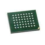
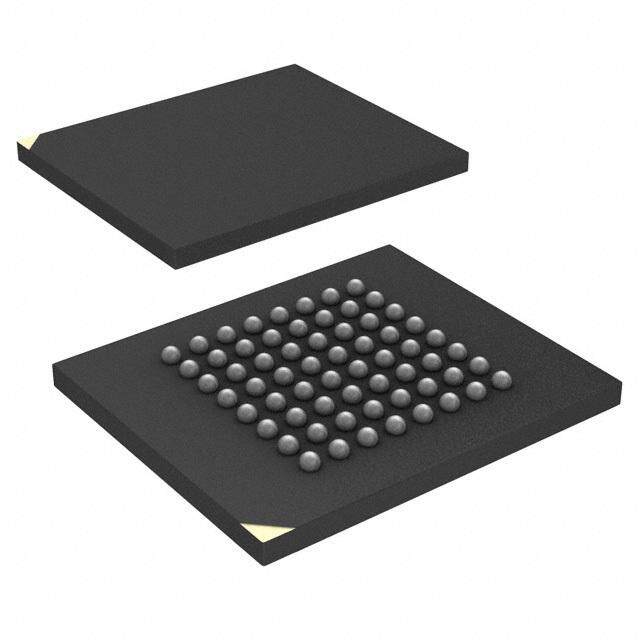
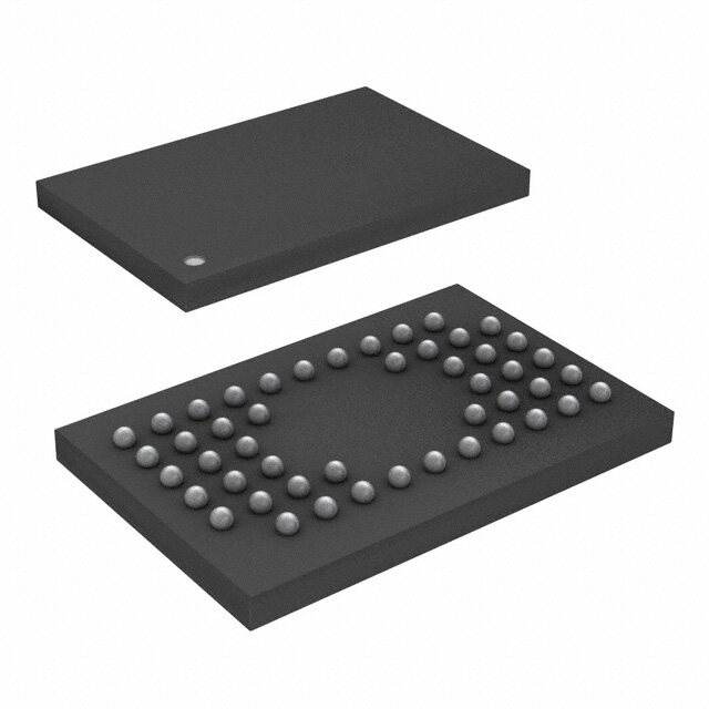
ICGOO电子元器件商城为您提供IS61WV25616BLL-10BLI由ISSI设计生产,在icgoo商城现货销售,并且可以通过原厂、代理商等渠道进行代购。 IS61WV25616BLL-10BLI价格参考¥18.43-¥18.43。ISSIIS61WV25616BLL-10BLI封装/规格:存储器, SRAM - 异步 存储器 IC 4Mb (256K x 16) 并联 10ns 48-迷你型BGA(6x8)。您可以下载IS61WV25616BLL-10BLI参考资料、Datasheet数据手册功能说明书,资料中有IS61WV25616BLL-10BLI 详细功能的应用电路图电压和使用方法及教程。
IS61WV25616BLL-10BLI 是由 ISSI(Integrated Silicon Solution, Inc.)生产的一款存储器芯片,属于静态随机存取存储器(SRAM)。其主要应用场景包括但不限于以下领域:

 1. 工业控制
   - 用于工业自动化设备中的数据缓存和临时存储,例如可编程逻辑控制器(PLC)、人机界面(HMI)等。
   - 在实时控制系统中提供快速的数据访问能力,确保系统运行的高效性和稳定性。

 2. 通信设备
   - 应用于路由器、交换机、基站等通信设备中,作为缓冲区或临时数据存储。
   - 支持高速数据传输和处理,满足通信系统的低延迟需求。

 3. 汽车电子
   - 适用于车载信息娱乐系统、驾驶辅助系统(ADAS)、仪表盘显示等场景。
   - 提供高可靠性和快速响应性能,适应汽车环境中苛刻的工作条件。

 4. 消费类电子产品
   - 用于数码相机、打印机、游戏机等需要高速数据处理的设备。
   - 提供临时存储功能,支持图像处理、音频/视频播放等操作。

 5. 网络与安全设备
   - 在防火墙、入侵检测系统(IDS)等网络安全设备中用作数据缓冲。
   - 确保数据包的快速处理和分析,提升网络安全性能。

 6. 医疗设备
   - 用于医疗成像设备(如超声波、CT扫描仪)和监护仪器中,存储实时采集的数据。
   - 满足医疗设备对高精度和低延迟的要求。

 特性总结
IS61WV25616BLL-10BLI 的高性能和可靠性使其成为需要快速数据访问和低延迟应用的理想选择。其典型参数包括 256K x 16 的存储容量、低功耗设计以及宽温度范围支持(通常为 -40°C 至 +85°C),适合多种复杂环境下的应用需求。
| 参数 | 数值 |
| 产品目录 | 集成电路 (IC) |
| 描述 | IC SRAM 4MBIT 10NS 48MINIBGA |
| 产品分类 | |
| 品牌 | ISSI, Integrated Silicon Solution Inc |
| 数据手册 | |
| 产品图片 |
|
| 产品型号 | IS61WV25616BLL-10BLI |
| rohs | 无铅 / 符合限制有害物质指令(RoHS)规范要求 |
| 产品系列 | - |
| 供应商器件封装 | 48-迷你型BGA(6x8) |
| 其它名称 | 706-1104 |
| 包装 | 托盘 |
| 存储器类型 | SRAM - 异步 |
| 存储容量 | 4M (256K x 16) |
| 封装/外壳 | 48-TFBGA |
| 工作温度 | -40°C ~ 85°C |
| 接口 | 并联 |
| 标准包装 | 480 |
| 格式-存储器 | RAM |
| 电压-电源 | 2.4 V ~ 3.6 V |
| 速度 | 10ns |


- 商务部:美国ITC正式对集成电路等产品启动337调查
- 曝三星4nm工艺存在良率问题 高通将骁龙8 Gen1或转产台积电
- 太阳诱电将投资9.5亿元在常州建新厂生产MLCC 预计2023年完工
- 英特尔发布欧洲新工厂建设计划 深化IDM 2.0 战略
- 台积电先进制程称霸业界 有大客户加持明年业绩稳了
- 达到5530亿美元!SIA预计今年全球半导体销售额将创下新高
- 英特尔拟将自动驾驶子公司Mobileye上市 估值或超500亿美元
- 三星加码芯片和SET,合并消费电子和移动部门,撤换高东真等 CEO
- 三星电子宣布重大人事变动 还合并消费电子和移动部门
- 海关总署:前11个月进口集成电路产品价值2.52万亿元 增长14.8%


PDF Datasheet 数据手册内容提取
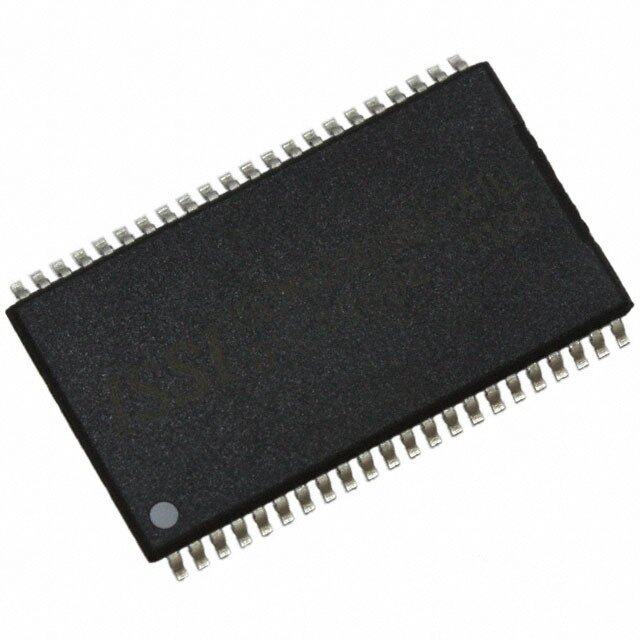
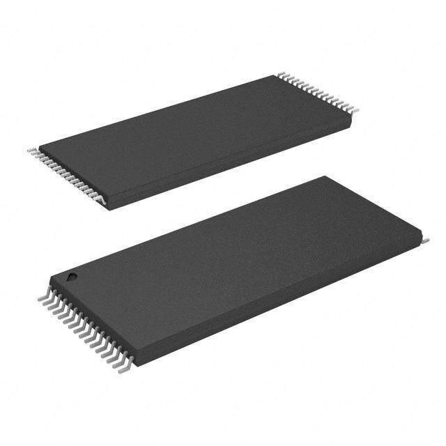
IS61WV25616ALL/ALS IS61WV25616BLL/BLS IS64WV25616BLL/BLS 256K x 16 HIGH SPEED ASYNCHRONOUS CMOS STATIC RAM FEBRUARY 2017 FEATURES DESCRIPTION HIGH SPEED: (IS61/64WV25616ALL/BLL) The ISSI IS61WV25616Axx/Bxx and IS64WV25616Bxx are high-speed, 4,194,304-bit static RAMs organized as • High-speed access time: 8, 10, 20 ns 262,144 words by 16 bits. It is fabricated using ISSI's high- • Low Active Power: 85 mW (typical) performance CMOS technology. This highly reliable process • Low Standby Power: 7 mW (typical) coupled with innovative circuit design techniques, yields CMOS standby high-performance and low power consumption devices. LOW POWER: (IS61/64WV25616ALS/BLS) When CE is HIGH (deselected), the device assumes a • High-speed access time: 25, 35, 45 ns standby mode at which the power dissipation can be re- • Low Active Power: 35 mW (typical) duced down with CMOS input levels. • Low Standby Power: 0.6 mW (typical) CMOS standby Easy memory expansion is provided by using Chip Enable • Single power supply and Output Enable inputs, CE and OE. The active LOW Write Enable (WE) controls both writing and reading of the — Vdd 1.65V to 2.2V (IS61WV25616Axx) memory. A data byte allows Upper Byte (UB) and Lower — Vdd 2.4V to 3.6V (IS61/64WV25616Bxx) Byte (LB) access. • Fully static operation: no clock or refresh required • Three state outputs The IS61WV25616Axx/Bxx and IS64WV25616Bxx are packaged in the JEDEC standard 44-pin 400mil SOJ, • Data control for upper and lower bytes 44-pin TSOP Type II and 48-pin Mini BGA (6mm x 8mm). • Industrial and Automotive temperature support • Lead-free available FUNCTIONAL BLOCK DIAGRAM 256K x 16 A0-A17 DECODER MEMORY ARRAY VDD GND I/O0-I/O7 Lower Byte I/O DATA COLUMN I/O I/O8-I/O15 CIRCUIT Upper Byte CE OE CONTROL WE CIRCUIT UB LB Copyright © 2017 Integrated Silicon Solution, Inc. All rights reserved. ISSI reserves the right to make changes to this specification and its products at any time without notice. ISSI assumes no liability arising out of the application or use of any information, products or services described herein. Customers are advised to obtain the lat- est version of this device specification before relying on any published information and before placing orders for products. Integrated Silicon Solution, Inc. does not recommend the use of any of its products in life support applications where the failure or malfunction of the product can reason- ably be expected to cause failure of the life support system or to significantly affect its safety or effectiveness. Products are not authorized for use in such applications unless Integrated Silicon Solution, Inc. receives written assurance to its satisfaction, that: a.) the risk of injury or damage has been minimized; b.) the user assume all such risks; and c.) potential liability of Integrated Silicon Solution, Inc is adequately protected under the circumstances Integrated Silicon Solution, Inc. — www.issi.com 1 Rev. H1 02/10/2017
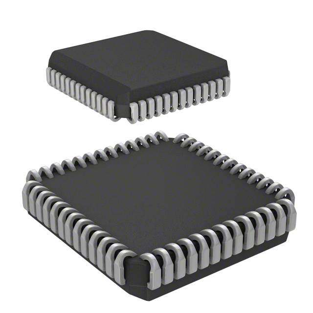
IS61WV25616ALL/ALS, IS61WV25616BLL/BLS, IS64WV25616BLL/BLS TRUTH TABLE I/O PIN Mode WE CE OE LB UB I/O0-I/O7 I/O8-I/O15 VDD Current Not Selected X H X X X High-Z High-Z Isb1, Isb2 Output Disabled H L H X X High-Z High-Z Icc X L X H H High-Z High-Z Read H L L L H dout High-Z Icc H L L H L High-Z dout H L L L L dout dout Write L L X L H dIn High-Z Icc L L X H L High-Z dIn L L X L L dIn dIn PIN CONFIGURATIONS PIN DESCRIPTIONS 44-Pin TSOP (Type II) and SOJ A0-A17 Address Inputs I/O0-I/O15 Data Inputs/Outputs CE Chip Enable Input OE Output Enable Input A0 1 44 A17 A1 2 43 A16 WE Write Enable Input A2 3 42 A15 LB Lower-byte Control (I/O0-I/O7) A3 4 41 OE UB Upper-byte Control (I/O8-I/O15) A4 5 40 UB CE 6 39 LB NC No Connection I/O0 7 38 I/O15 I/O1 8 37 I/O14 Vdd Power I/O2 9 36 I/O13 GND Ground I/O3 10 35 I/O12 VDD 11 34 GND GND 12 33 VDD I/O4 13 32 I/O11 I/O5 14 31 I/O10 I/O6 15 30 I/O9 I/O7 16 29 I/O8 WE 17 28 NC A5 18 27 A14 A6 19 26 A13 A7 20 25 A12 A8 21 24 A11 A9 22 23 A10 *soJ package under evaluation. 2 Integrated Silicon Solution, Inc. — www.issi.com Rev. H1 02/10/2017
IS61WV25616ALL/ALS, IS61WV25616BLL/BLS, IS64WV25616BLL/BLS PIN CONFIGURATIONS 44-Pin LQFP 48-Pin mini BGA (6mm x 8mm) 1 2 3 4 5 6 76543210 11111111EBB AAAAAAAAOUL 44 43 42 41 4039 38 37 36 35 34 CE 1 33 I/O15 I/O0 2 32 I/O14 A LB OE A0 A1 A2 N/C I/O1 3 31 I/O13 B I/O8 UB A3 A4 CE I/O0 I/O2 4 30 I/O12 I/O3 5 29 GND C I/O9 I/O10 A5 A6 I/O1 I/O2 TOP VIEW VDD 6 28 VDD D GND I/O11 A17 A7 I/O3 VDD GND 7 27 I/O11 E VDD I/O12 NC A16 I/O4 GND I/O4 8 26 I/O10 I/O5 9 25 I/O9 F I/O14 I/O13 A14 A15 I/O5 I/O6 I/O6 10 24 I/O8 G I/O15 NC A12 A13 WE I/O7 I/O7 11 23 NC H NC A8 A9 A10 A11 NC 12 13 14 15 1617 18 19 20 21 22 E0123456789 WAAAAAAAAAA *LQFP package under evaluation. PIN DESCRIPTIONS A0-A17 Address Inputs I/O0-I/O15 Data Inputs/Outputs CE Chip Enable Input OE Output Enable Input WE Write Enable Input LB Lower-byte Control (I/O0-I/O7) UB Upper-byte Control (I/O8-I/O15) NC No Connection Vdd Power GND Ground Integrated Silicon Solution, Inc. — www.issi.com 3 Rev. H1 02/10/2017
IS61WV25616ALL/ALS, IS61WV25616BLL/BLS, IS64WV25616BLL/BLS DC ELECTRICAL CHARACTERISTICS (Over Operating Range) VDD = 3.3V + 5% Symbol Parameter Test Conditions Min. Max. Unit VoH Output HIGH Voltage Vdd = Min., IoH = –4.0 mA 2.4 — V VoL Output LOW Voltage Vdd = Min., IoL = 8.0 mA — 0.4 V VIH Input HIGH Voltage 2 Vdd + 0.3 V VIL Input LOW Voltage(1) –0.3 0.8 V ILI Input Leakage GND ≤ VIn ≤ Vdd –1 1 µA ILo Output Leakage GND ≤ Vout ≤ Vdd, Outputs Disabled –1 1 µA Note: 1. VIL (min.) = –0.3V DC; VIL (min.) = –2.0V AC (pulse width < 20 ns). Not 100% tested. VIH (max.) = Vdd + 0.3V dc; VIH (max.) = Vdd + 2.0V Ac (pulse width < 20 ns). Not 100% tested. DC ELECTRICAL CHARACTERISTICS (Over Operating Range) VDD = 2.4V-3.6V Symbol Parameter Test Conditions Min. Max. Unit VoH Output HIGH Voltage Vdd = Min., IoH = –1.0 mA 1.8 — V VoL Output LOW Voltage Vdd = Min., IoL = 1.0 mA — 0.4 V VIH Input HIGH Voltage 2.0 Vdd + 0.3 V VIL Input LOW Voltage(1) –0.3 0.8 V ILI Input Leakage GND ≤ VIn ≤ Vdd –1 1 µA ILo Output Leakage GND ≤ Vout ≤ Vdd, Outputs Disabled –1 1 µA Note: 1. VIL (min.) = –0.3V DC; VIL (min.) = –2.0V AC (pulse width < 20 ns). Not 100% tested. VIH (max.) = Vdd + 0.3V dc; VIH (max.) = Vdd + 2.0V Ac (pulse width < 20 ns). Not 100% tested. DC ELECTRICAL CHARACTERISTICS (Over Operating Range) VDD = 1.65V-2.2V Symbol Parameter Test Conditions VDD Min. Max. Unit VoH Output HIGH Voltage IoH = -0.1 mA 1.65-2.2V 1.4 — V VoL Output LOW Voltage IoL = 0.1 mA 1.65-2.2V — 0.2 V VIH Input HIGH Voltage 1.65-2.2V 1.4 Vdd + 0.2 V VIL(1) Input LOW Voltage 1.65-2.2V –0.2 0.4 V ILI Input Leakage GND ≤ VIn ≤ Vdd –1 1 µA ILo Output Leakage GND ≤ Vout ≤ Vdd, Outputs Disabled –1 1 µA Note: 1. VIL (min.) = –0.3V DC; VIL (min.) = –2.0V AC (pulse width < 20 ns). Not 100% tested. VIH (max.) = Vdd + 0.3V dc; VIH (max.) = Vdd + 2.0V Ac (pulse width < 20 ns). Not 100% tested. 4 Integrated Silicon Solution, Inc. — www.issi.com Rev. H1 02/10/2017
IS61WV25616ALL/ALS, IS61WV25616BLL/BLS, IS64WV25616BLL/BLS AC TEST CONDITIONS Parameter Unit Unit Unit (2.4V-3.6V) (3.3V + 10%) (1.65V-2.2V) Input Pulse Level 0V to 3V 0V to 3V 0V to 1.8V Input Rise and Fall Times 1V/ ns 1V/ ns 1V/ ns Input and Output Timing 1.5V 1.5V 0.9V and Reference Level (VRef) Output Load See Figures 1 and 2 See Figures 1 and 2 See Figures 1 and 2 AC TEST LOADS 319 Ω ZO = 50Ω 50Ω 3.3V OUTPUT 1.5V OUTPUT 30 pF Including jig and 5 pF 353 Ω Including scope jig and scope Figure 1. Figure 2. Integrated Silicon Solution, Inc. — www.issi.com 5 Rev. H1 02/10/2017
IS61WV25616ALL/ALS, IS61WV25616BLL/BLS, IS64WV25616BLL/BLS ABSOLUTE MAXIMUM RATINGS(1) Symbol Parameter Value Unit Vterm Terminal Voltage with Respect to GND –0.5 to Vdd + 0.5 V Vdd Vdd Relates to GND –0.3 to 4.0 V tstg Storage Temperature –65 to +150 °C Pt Power Dissipation 1.0 W Notes: 1. Stress greater than those listed under ABSOLUTE MAXIMUM RATINGS may cause permanent damage to the device. This is a stress rating only and functional operation of the device at these or any other conditions above those indicated in the operational sections of this specification is not implied. Exposure to absolute maximum rating conditions for extended periods may affect reliability. CAPACITANCE(1,2) Symbol Parameter Conditions Max. Unit cIn Input Capacitance VIn = 0V 6 pF c Input/Output Capacitance Vout = 0V 8 pF I/o Notes: 1. Tested initially and after any design or process changes that may affect these parameters. 2. Test conditions: TA = 25°c, f = 1 MHz, Vdd = 3.3V. 6 Integrated Silicon Solution, Inc. — www.issi.com Rev. H1 02/10/2017
IS61WV25616ALL/ALS, IS61WV25616BLL/BLS, IS64WV25616BLL/BLS HIGH SPEED (IS61WV25616ALL/BLL) OPERATING RANGE (VDD) (IS61WV25616ALL) Range Ambient Temperature VDD Speed Commercial 0°C to +70°C 1.65V-2.2V 20ns Industrial –40°C to +85°C 1.65V-2.2V 20ns Automotive –40°C to +125°C 1.65V-2.2V 20ns OPERATING RANGE (VDD) (IS61WV25616BLL)(1) Range Ambient Temperature VDD (8 nS)1 VDD (10 nS)1 Commercial 0°C to +70°C 3.3V + 5% 2.4V-3.6V Industrial –40°C to +85°C 3.3V + 5% 2.4V-3.6V Note: 1. When operated in the range of 2.4V-3.6V, the device meets 10ns. When operated in the range of 3.3V + 5%, the device meets 8ns. OPERATING RANGE (VDD) (IS64WV25616BLL) Range Ambient Temperature VDD (10 nS) Automotive –40°C to +125°C 2.4V-3.6V POWER SUPPLY CHARACTERISTICS(1) (Over Operating Range) -8 -10 -20 Symbol Parameter Test Conditions Min. Max. Min. Max. Min. Max. Unit Icc Vdd Dynamic Operating Vdd = Max., Com. — 50 — 40 — 35 mA Supply Current Iout = 0 mA, f = fmAX Ind. — 55 — 45 — 40 Auto. — — — 65 — 60 typ.(2) 25 Icc1 Operating Vdd = Max., Com. — 35 — 35 — 30 mA Supply Current Iout = 0 mA, f = 0 Ind. — 40 — 40 — 40 Auto. — — — 60 — 60 Isb1 TTL Standby Current Vdd = Max., Com. — 10 — 10 — 10 mA (TTL Inputs) VIn = VIH or VIL Ind. — 15 — 15 — 15 CE ≥ VIH, f = 0 Auto. — — — 30 — 30 Isb2 CMOS Standby Vdd = Max., Com. — 8 — 8 — 8 mA Current (CMOS Inputs) CE ≥ Vdd – 0.2V, Ind. — 9 — 9 — 9 VIn ≥ Vdd – 0.2V, or Auto. — — — 20 — 20 VIn ≤ 0.2V, f = 0 typ.(2) 2 Note: 1. At f = fmAX, address and data inputs are cycling at the maximum frequency, f = 0 means no input lines change. 2. Typical values are measured at Vdd = 3.0V, TA = 25oC and not 100% tested. Integrated Silicon Solution, Inc. — www.issi.com 7 Rev. H1 02/10/2017
IS61WV25616ALL/ALS, IS61WV25616BLL/BLS, IS64WV25616BLL/BLS LOW POWER (IS61WV25616ALS/BLS) OPERATING RANGE (VDD) (IS61WV25616ALS) Range Ambient Temperature VDD Speed Commercial 0°C to +70°C 1.65V-2.2V 45ns Industrial –40°C to +85°C 1.65V-2.2V 45ns Automotive –40°C to +125°C 1.65V-2.2V 45ns OPERATING RANGE (VDD) (IS61WV25616BLS) Range Ambient Temperature VDD (25 nS) Commercial 0°C to +70°C 2.4V-3.6V Industrial –40°C to +85°C 2.4V-3.6V OPERATING RANGE (VDD) (IS64WV25616BLS) Range Ambient Temperature VDD (35 nS) Automotive –40°C to +125°C 2.4V-3.6V POWER SUPPLY CHARACTERISTICS(1) (Over Operating Range) -25 -35 -45 Symbol Parameter Test Conditions Min. Max. Min. Max. Min. Max. Unit Icc Vdd Dynamic Operating Vdd = Max., Com. — 20 — 20 — 15 mA Supply Current Iout = 0 mA, f = fmAX Ind. — 25 — 25 — 20 Auto. — 50 — 50 — 40 typ.(2) 11 Icc1 Operating Vdd = Max., Com. — 10 — 10 — 10 mA Supply Current Iout = 0 mA, f = 0 Ind. — 12 — 12 — 12 Auto. — 20 — 20 — 20 Isb1 TTL Standby Current Vdd = Max., Com. — 5 — 5 — 5 mA (TTL Inputs) VIn = VIH or VIL Ind. — 7 — 7 — 7 CE ≥ VIH, f = 0 Auto. — 10 — 10 — 10 Isb2 CMOS Standby Vdd = Max., Com. — 1 — 1 — 1 mA Current (CMOS Inputs) CE ≥ Vdd – 0.2V, Ind. — 2 — 2 — 2 VIn ≥ Vdd – 0.2V, or Auto. — 10 — 10 — 10 VIn ≤ 0.2V, f = 0 typ.(2) 0.2 Note: 1. At f = fmAX, address and data inputs are cycling at the maximum frequency, f = 0 means no input lines change. 2. Typical values are measured at Vdd = 3.0V, TA = 25oC and not 100% tested. 8 Integrated Silicon Solution, Inc. — www.issi.com Rev. H1 02/10/2017
IS61WV25616ALL/ALS, IS61WV25616BLL/BLS, IS64WV25616BLL/BLS READ CYCLE SWITCHING CHARACTERISTICS(1) (Over Operating Range) -8 -10 Symbol Parameter Min. Max. Min. Max. Unit trc Read Cycle Time 8 — 10 — ns tAA Address Access Time — 8 — 10 ns toHA Output Hold Time 2.0 — 2.0 — ns tAce CE Access Time — 8 — 10 ns tdoe OE Access Time — 4.5 — 4.5 ns tHzoe(2) OE to High-Z Output — 3 — 4 ns tLzoe(2) OE to Low-Z Output 0 — 0 — ns tHzce(2 CE to High-Z Output 0 3 0 4 ns tLzce(2) CE to Low-Z Output 3 — 3 — ns tbA LB, UB Access Time — 5.5 — 6.5 ns tHzb(2) LB, UB to High-Z Output 0 3 0 3 ns tLzb(2) LB, UB to Low-Z Output 0 — 0 — ns tPu Power Up Time 0 — 0 — ns tPd Power Down Time — 8 — 10 ns Notes: 1. Test conditions assume signal transition times of 3 ns or less, timing reference levels of 1.5V, input pulse levels of 0V to 3.0V and output loading specified in Figure 1. 2. Tested with the load in Figure 2. Transition is measured ±500 mV from steady-state voltage. Integrated Silicon Solution, Inc. — www.issi.com 9 Rev. H1 02/10/2017
IS61WV25616ALL/ALS, IS61WV25616BLL/BLS, IS64WV25616BLL/BLS READ CYCLE SWITCHING CHARACTERISTICS(1) (Over Operating Range) -20 ns -25 ns -35 ns -45ns Symbol Parameter Min. Max. Min. Max. Min. Max. Min. Max. Unit trc Read Cycle Time 20 — 25 — 35 — 45 — ns tAA Address Access Time — 20 — 25 — 35 — 45 ns toHA Output Hold Time 2.5 — 4 — 4 — 7 — ns tAce CE Access Time — 20 — 25 — 35 — 45 ns tdoe OE Access Time — 8 — 12 — 15 — 20 ns tHzoe(2) OE to High-Z Output 0 8 0 8 0 10 0 15 ns tLzoe(2) OE to Low-Z Output 0 — 0 — 0 — 0 — ns tHzce(2 CE to High-Z Output 0 8 0 8 0 10 0 15 ns tLzce(2) CE to Low-Z Output 3 — 10 — 10 — 15 — ns tbA LB, UB Access Time — 8 — 25 — 35 — 45 ns tHzb LB, UB to High-Z Output 0 8 0 8 0 10 0 15 ns tLzb LB, UB to Low-Z Output 0 — 0 — 0 — 0 — ns Notes: 1. Test conditions assume signal transition times of 1.5 ns or less, timing reference levels of 1.25V, input pulse levels of 0.4V to Vdd-0.3V and output loading specified in Figure 1a. 2. Tested with the load in Figure 1b. Transition is measured ±500 mV from steady-state voltage. Not 100% tested. 3. Not 100% tested. 10 Integrated Silicon Solution, Inc. — www.issi.com Rev. H1 02/10/2017
IS61WV25616ALL/ALS, IS61WV25616BLL/BLS, IS64WV25616BLL/BLS AC WAVEFORMS READ CYCLE NO. 1(1,2) (Address Controlled) (CE = OE = VIL, UB or LB = VIL) t RC ADDRESS t OHA t AA t OHA DOUT PREVIOUS DATA VALID DATA VALID READ1.eps READ CYCLE NO. 2(1,3) tRC ADDRESS tAA tOHA OE tDOE tHZOE CE tLZOE tACE tHZCE tLZCE LB, UB tLZB tBA tRC tHZB DOUT HIGH-Z DATA VALID ICC VDD tPU 50% tPD 50% Supply ISB Current UB_CEDR2.eps Notes: 1. WE is HIGH for a Read Cycle. 2. The device is continuously selected. OE, CE, UB, or LB = VIL. 3. Address is valid prior to or coincident with CE LOW transition. Integrated Silicon Solution, Inc. — www.issi.com 11 Rev. H1 02/10/2017
IS61WV25616ALL/ALS, IS61WV25616BLL/BLS, IS64WV25616BLL/BLS WRITE CYCLE SWITCHING CHARACTERISTICS(1,3) (Over Operating Range) -8 -10 Symbol Parameter Min. Max. Min. Max. Unit twc Write Cycle Time 8 — 10 — ns tsce CE to Write End 6.5 — 8 — ns tAw Address Setup Time 6.5 — 8 — ns to Write End tHA Address Hold from Write End 0 — 0 — ns tsA Address Setup Time 0 — 0 — ns tPwb LB, UB Valid to End of Write 6.5 — 8 — ns tPwe1 WE Pulse Width 6.5 — 8 — ns tPwe2 WE Pulse Width (OE = LOW) 8.0 — 10 — ns tsd Data Setup to Write End 5 — 6 — ns tHd Data Hold from Write End 0 — 0 — ns tHzwe(2) WE LOW to High-Z Output — 3.5 — 5 ns tLzwe(2) WE HIGH to Low-Z Output 2 — 2 — ns Notes: 1. Test conditions assume signal transition times of 3 ns or less, timing reference levels of 1.5V, input pulse levels of 0V to 3.0V and output loading specified in Figure 1. 2. Tested with the load in Figure 2. Transition is measured ±500 mV from steady-state voltage. Not 100% tested. 3. The internal write time is defined by the overlap of CE LOW and UB or LB, and WE LOW. All signals must be in valid states to initiate a Write, but any one can go inactive to terminate the Write. The Data Input Setup and Hold timing are referenced to the rising or falling edge of the signal that terminates the write. Shaded area product in development 12 Integrated Silicon Solution, Inc. — www.issi.com Rev. H1 02/10/2017
IS61WV25616ALL/ALS, IS61WV25616BLL/BLS, IS64WV25616BLL/BLS WRITE CYCLE SWITCHING CHARACTERISTICS(1,2) (Over Operating Range) -20 ns -25 ns -35 ns -45ns Symbol Parameter Min. Max. Min. Max. Min. Max. Min. Max. Unit twc Write Cycle Time 20 — 25 — 35 — 45 — ns tsce CE to Write End 12 — 18 — 25 — 35 — ns tAw Address Setup Time 12 — 15 — 25 — 35 — ns to Write End tHA Address Hold from Write End 0 — 0 — 0 — 0 — ns tsA Address Setup Time 0 — 0 — 0 — 0 — ns tPwb LB, UB Valid to End of Write 12 — 18 — 30 — 35 — ns tPwe1 WE Pulse Width (OE = HIGH) 12 — 18 — 30 — 35 — ns tPwe2 WE Pulse Width (OE = LOW) 17 — 20 — 30 — 35 — ns tsd Data Setup to Write End 9 — 12 — 15 — 20 — ns tHd Data Hold from Write End 0 — 0 — 0 — 0 — ns tHzwe(3) WE LOW to High-Z Output — 9 — 12 — 20 — 20 ns tLzwe(3) WE HIGH to Low-Z Output 3 — 5 — 5 — 5 — ns Notes: 1. Test conditions assume signal transition times of 1.5ns or less, timing reference levels of 1.25V, input pulse levels of 0.4V to Vdd- 0.3V and output loading specified in Figure 1a. 2. Tested with the load in Figure 1b. Transition is measured ±500 mV from steady-state voltage. Not 100% tested. 3. The internal write time is defined by the overlap of CE LOW and UB or LB, and WE LOW. All signals must be in valid states to initiate a Write, but any one can go inactive to terminate the Write. The Data Input Setup and Hold timing are referenced to the rising or falling edge of the signal that terminates the write. Integrated Silicon Solution, Inc. — www.issi.com 13 Rev. H1 02/10/2017
IS61WV25616ALL/ALS, IS61WV25616BLL/BLS, IS64WV25616BLL/BLS AC WAVEFORMS WRITE CYCLE NO. 1 (CE Controlled, OE is HIGH or LOW) (1 ) t WC ADDRESS VALID ADDRESS t SA t SCE t HA CE t AW t PWE1 WE t PWE2 t PBW UB, LB t HZWE t LZWE HIGH-Z DOUT DATA UNDEFINED t SD t HD DIN DATAIN VALID UB_CEWR1.eps Notes: 1. WRITE is an internally generated signal asserted during an overlap of the LOW states on the CE and WE inputs and at least one of the LB and UB inputs being in the LOW state. 2. WRITE = (CE) [ (LB) = (UB) ] (WE). WRITE CYCLE NO. 2 (WE Controlled. OE is HIGH During Write Cycle) (1,2) t WC ADDRESS VALID ADDRESS t HA OE CE LOW t AW t PWE1 WE t SA t PBW UB, LB t HZWE t LZWE HIGH-Z DOUT DATA UNDEFINED t SD t HD DIN DATAIN VALID UB_CEWR2.eps 14 Integrated Silicon Solution, Inc. — www.issi.com Rev. H1 02/10/2017
IS61WV25616ALL/ALS, IS61WV25616BLL/BLS, IS64WV25616BLL/BLS AC WAVEFORMS WRITE CYCLE NO. 3 (WE Controlled. OE is LOW During Write Cycle) (1) t WC ADDRESS VALID ADDRESS t HA OE LOW CE LOW t AW t PWE2 WE t SA t PBW UB, LB t HZWE t LZWE HIGH-Z DOUT DATA UNDEFINED t SD t HD DIN DATAIN VALID UB_CEWR3.eps WRITE CYCLE NO. 4 (LB, UB Controlled, Back-to-Back Write) (1,3) t WC t WC ADDRESS ADDRESS 1 ADDRESS 2 OE t SA CE LOW t HA t HA WE t SA t PBW t PBW UB, LB WORD 1 WORD 2 t HZWE t LZWE HIGH-Z DOUT DATA UNDEFINED t HD t HD t SD t SD DIN DVAATLAIDIN DVAATLAIDIN UB_CEWR4.eps Notes: 1. The internal Write time is defined by the overlap of CE = Low, UB and/or LB = Low, and WE = LOW. All signals must be in valid states to initiate a Write, but any can be deasserted to terminate the Write. The t sA, t HA, t sd, and t Hd timing is referenced to the rising or falling edge of the signal that terminates the Write. 2. Tested with OE HIGH for a minimum of 4 ns before WE = LOW to place the I/O in a HIGH-Z state. 3. WE may be held LOW across many address cycles and the LB, UB pins can be used to control the Write function. Integrated Silicon Solution, Inc. — www.issi.com 15 Rev. H1 02/10/2017
IS61WV25616ALL/ALS, IS61WV25616BLL/BLS, IS64WV25616BLL/BLS HIGH SPEED (IS61WV25616ALL/BLL) DATA RETENTION SWITCHING CHARACTERISTICS (2.4V-3.6V) Symbol Parameter Test Condition Options Min. Typ.(1) Max. Unit Vdr Vdd for Data Retention See Data Retention Waveform 2.0 — 3.6 V Idr Data Retention Current Vdd = 2.0V, CE ≥ Vdd – 0.2V Com. — 2 8 mA Ind. — — 9 Auto. 15 tsdr Data Retention Setup Time See Data Retention Waveform 0 — — ns trdr Recovery Time See Data Retention Waveform trc — — ns Note 1: Typical values are measured at Vdd = 3.0V, TA = 25oc and not 100% tested. DATA RETENTION SWITCHING CHARACTERISTICS (1.65V-2.2V) Symbol Parameter Test Condition Options Min. Typ.(1) Max. Unit Vdr Vdd for Data Retention See Data Retention Waveform 1.2 — 3.6 V Idr Data Retention Current Vdd = 1.2V, CE ≥ Vdd – 0.2V Com. — 5 10 mA Ind. — — 15 tsdr Data Retention Setup Time See Data Retention Waveform 0 — — ns trdr Recovery Time See Data Retention Waveform trc — — ns Note 1: Typical values are measured at Vdd = 1.8V, TA = 25oc and not 100% tested. DATA RETENTION WAVEFORM (CE Controlled) tSDR Data Retention Mode tRDR VDD VDR CE ≥ VDD - 0.2V CE GND 16 Integrated Silicon Solution, Inc. — www.issi.com Rev. H1 02/10/2017
IS61WV25616ALL/ALS, IS61WV25616BLL/BLS, IS64WV25616BLL/BLS LOW POWER (IS61WV25616ALS/BLS) DATA RETENTION SWITCHING CHARACTERISTICS (2.4V-3.6V) Symbol Parameter Test Condition Options Min. Typ.(1) Max. Unit Vdr Vdd for Data Retention See Data Retention Waveform 2.0 — 3.6 V Idr Data Retention Current Vdd = 2.0V, CE ≥ Vdd – 0.2V Com. — 0.2 1 mA Ind. — — 2 Auto. 10 tsdr Data Retention Setup Time See Data Retention Waveform 0 — — ns trdr Recovery Time See Data Retention Waveform trc — — ns Note 1: Typical values are measured at Vdd = 3.0V, TA = 25oc and not 100% tested. DATA RETENTION SWITCHING CHARACTERISTICS (1.65V-2.2V) Symbol Parameter Test Condition Options Min. Typ.(1) Max. Unit Vdr Vdd for Data Retention See Data Retention Waveform 1.2 — 3.6 V Idr Data Retention Current Vdd = 1.2V, CE ≥ Vdd – 0.2V Com. — 0.2 1 mA Ind. — — 2 tsdr Data Retention Setup Time See Data Retention Waveform 0 — — ns trdr Recovery Time See Data Retention Waveform trc — — ns Note 1: Typical values are measured at Vdd = 1.8V, TA = 25oc and not 100% tested. DATA RETENTION WAVEFORM (CE Controlled) tSDR Data Retention Mode tRDR VDD VDR CE ≥ VDD - 0.2V CE GND Integrated Silicon Solution, Inc. — www.issi.com 17 Rev. H1 02/10/2017
IS61WV25616ALL/ALS, IS61WV25616BLL/BLS, IS64WV25616BLL/BLS ORDERING INFORMATION (HIGH SPEED) Commercial Range: 0°C to +70°C Voltage Range: 2.4V to 3.6V Speed (ns) Order Part No. Package 10 (81) IS61WV25616BLL-10TL TSOP (Type II), Lead-free Note: 1. Speed = 8ns for Vdd = 3.3V + 5%. Speed = 10ns for Vdd = 2.4V to 3.6V. Industrial Range: -40°C to +85°C Voltage Range: 2.4V to 3.6V Speed (ns) Order Part No. Package 10 (81) IS61WV25616BLL-10BI 48 mini BGA (6mm x 8mm) IS61WV25616BLL-10BLI 48 mini BGA (6mm x 8mm), Lead-free IS61WV25616BLL-10TI TSOP (Type II) IS61WV25616BLL-10TLI TSOP (Type II), Lead-free IS61WV25616BLL-10KLI 400-mil SOJ, Lead-free Note: 1. Speed = 8ns for Vdd = 3.3V + 5%. Speed = 10ns for Vdd = 2.4V to 3.6V. Industrial Range: -40°C to +85°C Voltage Range: 1.65V to 2.2V Speed (ns) Order Part No. Package 20 IS61WV25616ALL-20BI 48 mini BGA (6mm x 8mm) IS61WV25616ALL-20TI TSOP (Type II) IS61WV25616ALL-20TLI TSOP (Type II), Lead-free Automotive Range: -40°C to +125°C Voltage Range: 2.4V to 3.6V Speed (ns) Order Part No. Package 10 IS64WV25616BLL-10BA3 48 mini BGA (6mm x 8mm) IS64WV25616BLL-10BLA3 48 mini BGA (6mm x 8mm), Lead-free IS64WV25616BLL-10CTA3 TSOP (Type II), Copper Leadframe IS64WV25616BLL-10CTLA3 TSOP (Type II), Lead-free, Copper Leadframe 18 Integrated Silicon Solution, Inc. — www.issi.com Rev. H1 02/10/2017
IS61WV25616ALL/ALS, IS61WV25616BLL/BLS, IS64WV25616BLL/BLS ORDERING INFORMATION (LOW POWER) Industrial Range: -40°C to +85°C Voltage Range: 2.4V to 3.6V Speed (ns) Order Part No. Package 25 IS61WV25616BLS-25TLI TSOP (Type II), Lead-free Industrial Range: -40°C to +85°C Voltage Range: 1.65V to 2.2V Speed (ns) Order Part No. Package 45 IS61WV25616ALS-45TLI TSOP (Type II), Lead-free Integrated Silicon Solution, Inc. — www.issi.com 19 Rev. H1 02/10/2017
IS61WV25616ALL/ALS, IS61WV25616BLL/BLS, IS64WV25616BLL/BLS 8 0 0 7 2 0 2/ .2 1 M- / O 8 MM 0 N :C OE D I SE NJ E: Mt n DIe m Gu Nc o I Ld L e O : c E TRen ne OT ONefer utli CR O N 1. 2. e g a k c a P 20 Integrated Silicon Solution, Inc. — www.issi.com Rev. H1 02/10/2017
IS61WV25616ALL/ALS, IS61WV25616BLL/BLS, IS64WV25616BLL/BLS 8 0 0 2 / 4 0 / 6 0 N. O SI U R N. NT SIO ON/I RU SI T U O R R T P O D PR OL R M A E MB D A U D e CL E n MM T IN LUD utli N : NO NC O SIO DO OT I e N 1 N g ME D E ES ka DI N O c NG D A b D Pa LI N N L O O TE : ONTRO MENSI MENSI O C DI DI N 1. 2. 3. Integrated Silicon Solution, Inc. — www.issi.com 21 Rev. H1 02/10/2017
IS61WV25616ALL/ALS, IS61WV25616BLL/BLS, IS64WV25616BLL/BLS 7 0 0 2 / 1 2 / 2 1 m m 1 0. n hi n. wit sio er u h sion . on/intr e anot OTE : Controlling dimension : mm Dimension D and E1 do not include mold protru Dimension b2 does not include dambar protrusi Formed leads shall be planar with respect to onat the seating plane after final test. Reference document : JEDEC SPEC MS-027. N 1. 2. 3. 4. 5. E N A L P G N TI A E S 22 Integrated Silicon Solution, Inc. — www.issi.com Rev. H1 02/10/2017
Mouser Electronics Authorized Distributor Click to View Pricing, Inventory, Delivery & Lifecycle Information: I SSI: IS61WV25616BLL-10TLI IS61WV25616BLL-10TLI-TR IS61WV25616BLL-10TL-TR IS64WV25616BLL-10BLA3 IS64WV25616BLL-10BLA3-TR IS61WV25616BLL-10BLI IS61WV25616BLL-10BLI-TR IS61WV25616BLL-10BI IS61WV25616BLL-10BI-TR IS61WV25616BLS-25TLI IS61WV25616BLS-25TLI-TR IS64WV25616BLL-10CTLA3 IS61WV25616BLL-10KLI-TR IS61WV25616BLL-10KLI