 Datasheet下载
- 型号: PC28F128P30TF65A
- 制造商: Micron Technology Inc
- 库位|库存: xxxx|xxxx
- 要求:
| 数量阶梯 | 香港交货 | 国内含税 |
| +xxxx | $xxxx | ¥xxxx |
查看当月历史价格
查看今年历史价格
PC28F128P30TF65A产品简介:
ICGOO电子元器件商城为您提供PC28F128P30TF65A由Micron Technology Inc设计生产,在icgoo商城现货销售,并且可以通过原厂、代理商等渠道进行代购。 PC28F128P30TF65A价格参考。Micron Technology IncPC28F128P30TF65A封装/规格:存储器, FLASH - NOR 存储器 IC 128Mb (8M x 16) 并联 52MHz 65ns 64-EasyBGA(10x13)。您可以下载PC28F128P30TF65A参考资料、Datasheet数据手册功能说明书,资料中有PC28F128P30TF65A 详细功能的应用电路图电压和使用方法及教程。
Micron Technology Inc.(美光科技)的PC28F128P30TF65A是一款存储器产品,具体属于NOR Flash存储器类别。这类存储器通常用于需要快速读取和执行代码的应用场景,特别是在嵌入式系统中。以下是该型号的具体应用场景:

 1. 嵌入式系统
   PC28F128P30TF65A常用于各种嵌入式系统中,如工业控制、消费电子、汽车电子等。它提供非易失性存储功能,能够在断电后保存数据,确保系统的稳定性和可靠性。例如,在智能家居设备、智能家电中,这款存储器可以用来存储固件和配置信息。

 2. 物联网(IoT)设备
   在物联网设备中,PC28F128P30TF65A可用于存储设备的启动代码、操作系统映像以及关键数据。由于其低功耗和快速读取特性,特别适合用于传感器节点、网关和其他边缘计算设备,能够有效减少延迟并提高响应速度。

 3. 汽车电子
   汽车行业中,这款存储器广泛应用于车载娱乐系统、导航系统、车身控制系统等。它能够存储车辆的控制程序、诊断数据和用户设置等信息,确保车辆在各种环境下的正常运行。此外,其高可靠性和耐久性也使其适用于严苛的汽车环境。

 4. 通信设备
   在通信设备中,PC28F128P30TF65A可用于存储路由器、交换机、基站等设备的引导程序和配置文件。它的快速读取速度有助于缩短设备的启动时间,并确保在网络中断或重启后能够迅速恢复正常工作。

 5. 医疗设备
   医疗设备对存储器的可靠性和稳定性要求极高,PC28F128P30TF65A凭借其出色的性能和耐用性,被广泛应用于医疗仪器中,如心电图机、监护仪等。它可以存储设备的操作系统、应用程序以及患者的诊断数据,确保医疗设备的高效运行和数据的安全性。

 总结
PC28F128P30TF65A作为一款高性能的NOR Flash存储器,适用于多种需要快速读取和高可靠性的应用场景,尤其在嵌入式系统、物联网、汽车电子、通信设备和医疗设备等领域表现出色。其低功耗、快速读取和高可靠性等特点,使其成为众多行业中的理想选择。
| 参数 | 数值 |
| 产品目录 | 集成电路 (IC) |
| 描述 | IC FLASH 128MBIT 65NS 64EASYBGA |
| 产品分类 | |
| 品牌 | Micron Technology Inc |
| 数据手册 | |
| 产品图片 |
|
| 产品型号 | PC28F128P30TF65A |
| rohs | 无铅 / 符合限制有害物质指令(RoHS)规范要求 |
| 产品系列 | StrataFlash™ |
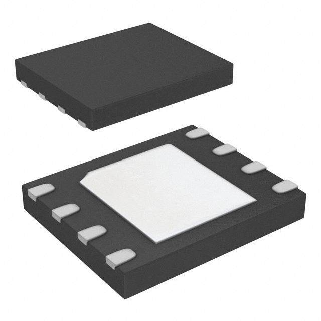
| 供应商器件封装 | 64-EasyBGA (10x13) |
| 包装 | 托盘 |
| 存储器类型 | FLASH - NOR |
| 存储容量 | 128M (8M x 16) |
| 封装/外壳 | 64-TFBGA |
| 工作温度 | -40°C ~ 85°C |
| 接口 | 并联 |
| 标准包装 | 864 |
| 格式-存储器 | 闪存 |
| 电压-电源 | 1.7 V ~ 2 V |
| 速度 | 65ns |


- 商务部:美国ITC正式对集成电路等产品启动337调查
- 曝三星4nm工艺存在良率问题 高通将骁龙8 Gen1或转产台积电
- 太阳诱电将投资9.5亿元在常州建新厂生产MLCC 预计2023年完工
- 英特尔发布欧洲新工厂建设计划 深化IDM 2.0 战略
- 台积电先进制程称霸业界 有大客户加持明年业绩稳了
- 达到5530亿美元!SIA预计今年全球半导体销售额将创下新高
- 英特尔拟将自动驾驶子公司Mobileye上市 估值或超500亿美元
- 三星加码芯片和SET,合并消费电子和移动部门,撤换高东真等 CEO
- 三星电子宣布重大人事变动 还合并消费电子和移动部门
- 海关总署:前11个月进口集成电路产品价值2.52万亿元 增长14.8%


PDF Datasheet 数据手册内容提取
® Numonyx Axcell™ P30-65nm Flash Memory 128-Mbit, 64-Mbit Single Bit per Cell (SBC) Datasheet Product Features (cid:132) High Performance: (cid:132) Enhanced Security: — 65ns initial access time for Easy BGA and — Absolute write protection: VPP = Vss QUAD+ — Power-transition erase/program lockout — 75ns initial access time for TSOP — Individual zero-latency block locking — 25ns 8-word asynchronous-page read mode — Individual block lock-down capability — 52MHz with zero WAIT states, 17ns clock-to- — Password Access feature data output synchronous-burst read mode — One-Time Programmable Register: — 4-, 8-, 16- and continuous-word options for — 64 OTP bits, programmed with unique burst mode information by Numonyx — 1.8V Low Power buffered programming at — 2112 OTP bits, available for customer 1.8MByte/s (Typ) using 256-word buffer programming — Buffered Enhanced Factory Programming at 3.2MByte/s (typ) using 256-word buffer (cid:132) Software: — 20µs (Typ) program suspend (cid:132) Architecture: — 20µs (Typ) erase suspend — Asymmetrically-blocked architecture — Basic Command Set and Extended Function — Four 32-KByte parameter blocks: top or Interface (EFI) Command Set compatible bottom configuration — Common Flash Interface capable — 128-KByte array blocks — Blank Check to verify an erased block (cid:132) Density and Packaging: — 56-Lead TSOP (128-Mbit, 64-Mbit) (cid:132) Voltage and Power: — 64-Ball Easy BGA (128-Mbit, 64-Mbit) — VCC (core) voltage: 1.7V – 2.0V — 88-Ball QUAD+ Package (128-Mbit) — VCCQ (I/O) voltage: 1.7V – 3.6V — 16-bit wide data bus — Standby current: 30µA(Typ)/55µA(Max) — Continuous synchronous read current: 23mA (cid:132) Quality and Reliability: (Typ)/28mA (Max) at 52MHz — JESD47E Compliant — Operating temperature: –40°C to +85°C — Minimum 100,000 erase cycles — 65nm process technology Datasheet Apr 2010 1 Order Number: 208033-02
LIegNal LFinesO andR DisMclaimAersTION IN THIS DOCUMENT IS PROVIDED IN CONNECTION WITH NUMONYX™ PRODUCTS. NO LICENSE, EXPRESS OR IMPLIED, BY ESTOPPEL OR OTHERWISE, TO ANY INTELLECTUAL PROPERTY RIGHTS IS GRANTED BY THIS DOCUMENT. EXCEPT AS PROVIDED IN NUMONYX'S TERMS AND CONDITIONS OF SALE FOR SUCH PRODUCTS, NUMONYX ASSUMES NO LIABILITY WHATSOEVER, AND NUMONYX DISCLAIMS ANY EXPRESS OR IMPLIED WARRANTY, RELATING TO SALE AND/OR USE OF NUMONYX PRODUCTS INCLUDING LIABILITY OR WARRANTIES RELATING TO FITNESS FOR A PARTICULAR PURPOSE, MERCHANTABILITY, OR INFRINGEMENT OF ANY PATENT, COPYRIGHT OR OTHER INTELLECTUAL PROPERTY RIGHT. Numonyx products are not intended for use in medical, life saving, life sustaining, critical control or safety systems, or in nuclear facility applications. Numonyx may make changes to specifications and product descriptions at any time, without notice. Numonyx, B.V. may have patents or pending patent applications, trademarks, copyrights, or other intellectual property rights that relate to the presented subject matter. The furnishing of documents and other materials and information does not provide any license, express or implied, by estoppel or otherwise, to any such patents, trademarks, copyrights, or other intellectual property rights. Designers must not rely on the absence or characteristics of any features or instructions marked “reserved” or “undefined.” Numonyx reserves these for future definition and shall have no responsibility whatsoever for conflicts or incompatibilities arising from future changes to them. Contact your local Numonyx sales office or your distributor to obtain the latest specifications and before placing your product order. Copies of documents which have an order number and are referenced in this document, or other Numonyx literature may be obtained by visiting Numonyx's website at http://www.numonyx.com. Numonyx, the Numonyx logo, and Axcell are trademarks or registered trademarks of Numonyx , B.V. or its subsidiaries in other countries. *Other names and brands may be claimed as the property of others. Copyright © 2010, Numonyx, B.V., All Rights Reserved. Datasheet Apr 2010 2 Order Number: 208033-02
P30-65nm SBC Contents 1.0 Functional Description...............................................................................................5 1.1 Introduction.......................................................................................................5 1.2 Overview ...........................................................................................................5 1.3 Memory Map.......................................................................................................6 2.0 Package Information.................................................................................................7 2.1 56-Lead TSOP.....................................................................................................7 2.2 64-Ball Easy BGA Package....................................................................................8 2.3 QUAD+ SCSP Packages......................................................................................10 3.0 Pinouts/Ballouts .....................................................................................................11 4.0 Signals....................................................................................................................14 5.0 Bus Operations........................................................................................................16 5.1 Read - Asynchronous Mode.................................................................................16 5.2 Read - Synchronous Mode..................................................................................16 5.3 Write...............................................................................................................17 5.4 Output Disable..................................................................................................17 5.5 Standby...........................................................................................................17 5.6 Reset...............................................................................................................18 6.0 Command Set..........................................................................................................19 6.1 Device Command Codes.....................................................................................19 6.2 Device Command Bus Cycles..............................................................................20 7.0 Read Operation........................................................................................................22 7.1 Read Array.......................................................................................................22 7.2 Read Device Identifier........................................................................................22 7.3 Read CFI..........................................................................................................23 7.4 Read Status Register.........................................................................................23 7.5 Clear Status Register.........................................................................................23 8.0 Program Operation..................................................................................................24 8.1 Word Programming ...........................................................................................24 8.2 Buffered Programming.......................................................................................24 8.3 Buffered Enhanced Factory Programming..............................................................25 8.4 Program Suspend..............................................................................................27 8.5 Program Resume...............................................................................................28 8.6 Program Protection............................................................................................28 9.0 Erase Operation.......................................................................................................29 9.1 Block Erase......................................................................................................29 9.2 Blank Check.....................................................................................................29 9.3 Erase Suspend..................................................................................................30 9.4 Erase Resume...................................................................................................30 9.5 Erase Protection................................................................................................30 10.0 Security...................................................................................................................31 10.1 Block Locking....................................................................................................31 10.2 Selectable OTP Blocks........................................................................................33 10.3 Password Access...............................................................................................33 11.0 Register...................................................................................................................34 11.1 Status Register (SR)..........................................................................................34 11.2 Read Configuration Register (RCR)......................................................................34 Datasheet Apr 2010 3 Order Number: 208033-02
P30-65nm SBC 11.3 One-Time Programmable (OTP) Registers.............................................................40 12.0 Power and Reset Specifications ...............................................................................43 12.1 Power-Up and Power-Down.................................................................................43 12.2 Reset Specifications...........................................................................................43 12.3 Power Supply Decoupling....................................................................................44 13.0 Maximum Ratings and Operating Conditions............................................................45 13.1 Absolute Maximum Ratings.................................................................................45 13.2 Operating Conditions..........................................................................................45 14.0 Electrical Specifications...........................................................................................46 14.1 DC Current Characteristics..................................................................................46 14.2 DC Voltage Characteristics..................................................................................47 15.0 AC Characteristics....................................................................................................48 15.1 AC Test Conditions.............................................................................................48 15.2 Capacitance......................................................................................................49 15.3 AC Read Specifications ......................................................................................50 15.4 AC Write Specifications.......................................................................................54 15.5 Program and Erase Characteristics.......................................................................58 16.0 Ordering Information...............................................................................................59 A Supplemental Reference Information.......................................................................61 A.1 Common Flash Interface.....................................................................................61 A.2 Flowcharts........................................................................................................73 A.3 Write State Machine...........................................................................................83 B Conventions - Additional Documentation .................................................................87 B.1 Acronyms.........................................................................................................87 B.2 Definitions and Terms ........................................................................................87 C Revision History.......................................................................................................89 Datasheet Apr 2010 4 Order Number: 208033-02
P30-65nm SBC 1.0 Functional Description 1.1 Introduction This document provides information about the Numonyx® AxcellTM P30-65nm Single Bit per Cell (SBC) Flash memory and describes its features, operations, and specifications. P30-65nm SBC device is offered in 64-Mbit and 128-Mbit. Benefits include high-speed interface NOR device, and support for code and data storage. Features include high- performance synchronous-burst read mode, a dramatical improvement in buffer program time through larger buffer size, fast asynchronous access times, low power, flexible security options, and three industry-standard package choices. P30-65nm SBC device is manufactured using 65nm process technology. 1.2 Overview P30-65nm SBC device provides high performance on a 16-bit data bus. Individually erasable memory blocks are sized for optimum code and data storage. Upon initial power-up or return from reset, the device defaults to asynchronous page-mode read. Configuring the Read Configuration Register (RCR) enables synchronous burst-mode reads. In synchronous burst mode, output data is synchronized with a user-supplied clock signal. A WAIT signal provides easy CPU-to-flash memory synchronization. In addition to the enhanced architecture and interface, the device incorporates technology that enables fast buffer program and erase operations. The device features a 256-word buffer to enable optimum programming performance, which can improve system programming throughput time significantly to 1.8MByte/s. Designed for low-voltage systems, the P30-65nm SBC device supports read operations with VCC at 1.8V, and erase and program operations with VPP at 1.8V or 9.0V. Buffered Enhanced Factory Programming provides the fastest flash array programming performance with VPP at 9.0V, which increases factory throughput with 3.2Mbyte/s. With VPP at 1.8V, VCC and VPP can be tied together for a simple, ultra low power design. In addition to voltage flexibility, a dedicated VPP connection provides complete data protection when VPP ≤ V . PPLK The Command User Interface is the interface between the system processor and all internal operations of the device. An internal Write State Machine automatically executes the algorithms and timings necessary for block erase and program. A Status Register indicates erase or program completion and any errors that may have occurred. A device command sequence invokes program and erase automation. Each erase operation erases one block. The Erase Suspend feature allows system software to pause an erase cycle to read or program data in another block. Program Suspend allows system software to pause programming to read other locations. The OTP Register allows unique flash device identification that can be used to increase system security. The individual Block Lock feature provides zero-latency block locking and unlocking. The P30-65nm SBC device adds enhanced protection via Password Access; this new feature allows write and/or read access protection of user-defined blocks. In addition, the P30-65nm SBC device also has backward-compatible One-Time Programmable (OTP) permanent block locking security feature. Datasheet Apr 2010 5 Order Number:208033-02
P30-65nm SBC 1.3 Memory Map Figure 1: P30-65nm SBC Memory Map (64-Mbit and 128-Mbit Densities) A<23:1> 128-Mbit A<22:1> 64-Mbit 7F0000 –7FFFFF 64-Kword Block 130 3F0000–3FFFFF 64-Kword Block 66 Mbit 020000 –02FFFF 64-Kword Block 5 4-Mbit 128- 6 010000 –01FFFF 64-Kword Block 4 00C000–00FFFF 16-Kword Block 3 008000 –00BFFF 16-Kword Block 2 004000 –007FFF 16-Kword Block 1 000000 –003FFF 16-Kword Block 0 Bottom Boot Word Wide (x16) Mode A<23:1> 128-Mbit 7FC000– 7FFFFF 16-Kword Block 130 7F8000– 7FBFFF 16-Kword Block 129 7F4000– 7F7000 16-Kword Block 128 7F0000 – 7F3FFF 16-Kword Block 127 A<22:1> 64-Mbit 7E0000 – 7EFFFF 64-Kword Block 126 3FC000 – 3FFFFF 16-Kword Block 66 3F8000– 3FBFFF 16-Kword Block 65 3F4000– 3F7FFF 16-Kword Block 64 Mbit 3F0000– 3F3FFF 16-Kword Block 63 8- 3E0000– 3EFFFF 64-Kword Block 62 12 Mbit 64- 010000– 01FFFF 64-Kword Block 1 010000– 01FFFF 64-Kword Block 1 000000– 00FFFF 64-Kword Block 0 000000– 00FFFF 64-Kword Block 0 Top Boot Top Boot Word Wide (x16) Mode Word Wide (x16) Mode Note: A1 is the least significant address bit for TSOP and Easy BGA while A0 for the QUAD+ package. Unless otherwise indicated, for the purpose of brevity, this document will consolidate all discussions to A1 as the least significant Address bit. Datasheet Apr 2010 6 Order Number: 208033-02
P30-65nm SBC 2.0 Package Information 2.1 56-Lead TSOP Figure 2: TSOP Mechanical Specifications Z See Notes 1 and 3 See Note 2 A2 Pin 1 e E See Detail B Y D1 A1 D Seating Plane See Detail A A Detail A Detail B C 0 b L Table 1: TSOP Package Dimensions (Sheet 1 of 2) Millimeters Inches Product Information Symbol Min Nom Max Min Nom Max Package Height A - - 1.200 - - 0.047 Standoff A1 0.050 - - 0.002 - - Package Body Thickness A2 0.965 0.995 1.025 0.038 0.039 0.040 Lead Width b 0.100 0.150 0.200 0.004 0.006 0.008 Lead Thickness C 0.100 0.150 0.200 0.004 0.006 0.008 Package Body Length D1 18.200 18.400 18.600 0.717 0.724 0.732 Package Body Width E 13.800 14.000 14.200 0.543 0.551 0.559 Lead Pitch e - 0.500 - - 0.0197 - Terminal Dimension D 19.800 20.00 20.200 0.780 0.787 0.795 Lead Tip Length L 0.500 0.600 0.700 0.020 0.024 0.028 Datasheet Apr 2010 7 Order Number:208033-02
P30-65nm SBC Table 1: TSOP Package Dimensions (Sheet 2 of 2) Millimeters Inches Product Information Symbol Min Nom Max Min Nom Max Lead Count N - 56 - - 56 - Lead Tip Angle θ 0° 3° 5° 0° 3° 5° Seating Plane Coplanarity Y - - 0.100 - - 0.004 Lead to Package Offset Z 0.150 0.250 0.350 0.006 0.010 0.014 Notes: 1. One dimple on package denotes Pin 1. 2. If two dimples, then the larger dimple denotes Pin 1. 3. Pin 1 will always be in the upper left corner of the package, in reference to the product mark. 2.2 64-Ball Easy BGA Package Figure 3: Easy BGA Mechanical Specifications (10x13x1.2 mm) S1 Ball A1 Ball A1 Corner D Corner 1 2 3 4 5 6 7 8 8 7 6 5 4 3 2 1 S2 A A B B C C D D b E E E F F G G e H H Top View -Ball side down Bottom View -Ball Side Up A1 A2 A Seating Y Plane Note: Drawing not to scale Table 2: Easy BGA Package Dimensions for 10x13x1.2 mm (Sheet 1 of 2) Millimeters Inches Product Information Symbol Min Nom Max Min Nom Max Package Height A - - 1.200 - - 0.0472 Ball Height A1 0.250 - - 0.0098 - - Package Body Thickness A2 - 0.780 - - 0.0307 - Ball (Lead) Width b 0.310 0.410 0.510 0.0120 0.0160 0.0200 Package Body Width D 9.900 10.000 10.100 0.3898 0.3937 0.3976 Datasheet Apr 2010 8 Order Number: 208033-02
P30-65nm SBC Table 2: Easy BGA Package Dimensions for 10x13x1.2 mm (Sheet 2 of 2) Millimeters Inches Product Information Symbol Min Nom Max Min Nom Max Package Body Length E 12.900 13.000 13.100 0.5079 0.5118 0.5157 Pitch e - 1.000 - - 0.0394 - Ball (Lead) Count N - 64 - - 64 - Seating Plane Coplanarity Y - - 0.100 - - 0.0039 Corner to Ball A1 Distance Along D S1 1.400 1.500 1.600 0.0551 0.0591 0.0630 Corner to Ball A1 Distance Along E S2 2.900 3.000 3.100 0.1142 0.1181 0.1220 Note: Daisy Chain Evaluation Unit information is at Numonyx™ Flash Memory Packaging Technology http:// developer.Numonyx.com/design/flash/packtech. Datasheet Apr 2010 9 Order Number:208033-02
P30-65nm SBC 2.3 QUAD+ SCSP Packages Figure 4: 128-Mbit, 88-ball (80 active) QUAD+ SCSP Specifications (8x10x1.2 mm) A1 Index S Mark 1 1 2 3 4 5 6 7 8 8 7 6 5 4 3 2 1 S A A 2 B B C C D D E E F F D e G G H H J J K K L L M M b E Top View -Ball Bottom View -Ball Up Down A 2 A1 A Y Drawing not to scale. Millimeters Inches Dimensions Symbol Min Nom Max Min Nom Max Package Height A - - 1.200 - - 0.0472 Ball Height A1 0.200 - - 0.0079 - - Package Body Thickness A2 - 0.860 - - 0.0339 - Ball (Lead) Width b 0.325 0.375 0.425 0.0128 0.0148 0.0167 Package Body Width D 9.900 10.000 10.100 0.3898 0.3937 0.3976 Package Body Length E 7.900 8.000 8.100 0.3110 0.3150 0.3189 Pitch e - 0.800 - - 0.0315 - Ball (Lead) Count N - 88 - - 88 - Seating Plane Coplanarity Y - - 0.100 - - 0.0039 Corner to Ball A1 Distance Along E S1 1.100 1.200 1.300 0.0433 0.0472 0.0512 Corner to Ball A1 Distance Along D S2 0.500 0.600 0.700 0.0197 0.0236 0.0276 Datasheet Apr 2010 10 Order Number: 208033-02
P30-65nm SBC 3.0 Pinouts/Ballouts Figure 5: 56-Lead TSOP Pinout (64-Mbit and 128-Mbit Densities) A16 1 56 WAIT A15 2 55 A17 A14 3 54 DQ15 A13 4 53 DQ7 A12 5 52 DQ14 A11 6 51 DQ6 A10 7 50 DQ13 A9 8 49 DQ5 A23 9 48 DQ12 A22 10 47 DQ4 A21 11 46 ADV# VSS 12 45 CLK NC 13 56-Lead TSOP Pinout 44 RST# WE# 14 14 mm x 20 mm 43 VPP WP# 15 42 DQ11 A20 16 Top View 41 DQ3 A19 17 40 DQ10 A18 18 39 DQ2 A8 19 38 VCCQ A7 20 37 DQ9 A6 21 36 DQ1 A5 22 35 DQ8 A4 23 34 DQ0 A3 24 33 VCC A2 25 32 OE# RFU 26 31 VSS RFU 27 30 CE# VSS 28 29 A1 Notes: 1. A1 is the least significant address bit. 2. A23 is valid for 128-Mbit densities; otherwise, it is a no connect (NC). 3. A22 is valid for 64-Mbit densities and above; otherwise, it is a no connect (NC). 4. No Internal Connection on Pin 13; it may be driven or floated. For legacy 130nm designs, this pin can be tied to Vcc. 5. One dimple on package denotes Pin 1 which will always be in the upper left corner of the package, in reference to the product mark. Datasheet Apr 2010 11 Order Number:208033-02
P30-65nm SBC Figure 6: 64-Ball Easy BGA Ballout (64-Mbit and 128-Mbit Densities) 1 2 3 4 5 6 7 8 8 7 6 5 4 3 2 1 A A A1 A6 A8 VPP A13 VCC A18 A22 A22 A18 VCC A13 VPP A8 A6 A1 B B A2 VSS A9 CE# A14 RFU A19 RFU RFU A19 RFU A14 CE# A9 VSS A2 C C A3 A7 A10 A12 A15 WP# A20 A21 A21 A20 WP# A15 A12 A10 A7 A3 D D A4 A5 A11 RST#VCCQVCCQ A16 A17 A17 A16 VCCQVCCQRST# A11 A5 A4 E E DQ8 DQ1 DQ9 DQ3 DQ4 CLK DQ15 RFU RFU DQ15 CLK DQ4 DQ3 DQ9 DQ1 DQ8 F F RFU DQ0 DQ10DQ11DQ12 ADV# WAIT OE# OE# WAIT ADV#DQ12DQ11 DQ10 DQ0 RFU G G A23 RFU DQ2 VCCQ DQ5 DQ6 DQ14 WE# WE# DQ14 DQ6 DQ5 VCCQ DQ2 RFU A23 H H RFU VSS VCC VSS DQ13 VSS DQ7 RFU RFU DQ7 VSS DQ13 VSS VCC VSS RFU Easy BGA Easy BGA Top View-Ball side down Bottom View-Ball side up Notes: 1. A1 is the least significant address bit. 2. A23 is valid for 128-Mbit densities; otherwise, it is a no connect. 3. A22 is valid for 64-Mbit densities and above; otherwise, it is a no connect (NC). 4. One dimple on package denotes Pin 1 which will always be in the upper left corner of the package, in reference to the product mark. Datasheet Apr 2010 12 Order Number: 208033-02
P30-65nm SBC Figure 7: QUAD+ SCSP Ballout and Signals (128-Mbit) Pin 1 1 2 3 4 5 6 7 8 A DU DU Depop Depop Depop Depop DU DU A B A4 A18 A19 VSS VCC VCC A21 A11 B C A5 RFU RFU VSS RFU CLK A22 A12 C D A3 A17 RFU VPP RFU RFU A9 A13 D E A2 A7 RFU WP# ADV# A20 A10 A15 E F A1 A6 RFU RST# WE# A8 A14 A16 F G A0 DQ8 DQ2 DQ10 DQ5 DQ13 WAIT F2-CE# G H RFU DQ0 DQ1 DQ3 DQ12 DQ14 DQ7 F2-OE# H J RFU F1-OE# DQ9 DQ11 DQ4 DQ6 DQ15 VCCQ J K F1-CE# RFU RFU RFU RFU VCC VCCQ RFU K L VSS VSS VCCQ VCC VSS VSS VSS VSS L M DU DU Depop Depop Depop Depop DU DU M 1 2 3 4 5 6 7 8 Top View -Ball Side Down Control Signals De-Populated Ball Address Legends: Reserved for Future Use Data Do Not Use Power/Ground Notes: 1. A22 is valid for 128-Mbit densities; otherwise, it is a no connect (NC). 2. A21 is valid for 64-Mbit densities and above; otherwise, it is a no connect (NC). 3. F2-CE# and F2-OE# are no connect (NC) for all densities. 4. Unlike TSOP and Easy BGA, A0 is the least significant address bit for the QUAD+ package. Unless otherwise indicated, for the purpose of brevity, this document will consolidate all later discussions to A1 as the least significant Address bit. Datasheet Apr 2010 13 Order Number:208033-02
P30-65nm SBC 4.0 Signals Table 3: TSOP and Easy BGA Signal Descriptions Symbol Type Name and Function A[MAX:1] Input ADDRESS INPUTS: Device address inputs. 128-Mbit: A[23:1], 64-Mbit: A[22:1]. DATA INPUT/OUTPUTS: Inputs data and commands during write cycles; outputs data during Input/ DQ[15:0] reads of memory, Status Register, OTP Register, and Read Configuration Register. Data balls float Output when the CE# or OE# are deasserted. Data is internally latched during writes. ADDRESS VALID: Active low input. During synchronous read operations, addresses are latched on the rising edge of ADV#, or on the next valid CLK edge with ADV# low, whichever occurs first. ADV# Input In asynchronous mode, the address is latched when ADV# going high or continuously flows through if ADV# is held low. WARNING: Designs not using ADV# must tie it to VSS to allow addresses to flow through. CHIP ENABLE: Active low input. CE# low selects the associated flash memory die. When asserted, flash internal control logic, input buffers, decoders, and sense amplifiers are active. When CE# Input deasserted, the associated flash die is deselected, power is reduced to standby levels, data and WAIT outputs are placed in high-Z state. WARNING: Chip Enable must be high when device is not in use. CLOCK: Synchronizes the device with the system’s bus frequency in synchronous-read mode. During synchronous read operations, addresses are latched on the rising edge of ADV#, or on the CLK Input next valid CLK edge with ADV# low, whichever occurs first. WARNING: Designs not using CLK for synchronous read mode must tie it to VCCQ or VSS. OUTPUT ENABLE: Active low input. OE# low enables the device’s output data buffers during read OE# Input cycles. OE# high places the data outputs and WAIT in High-Z. RESET: Active low input. RST# resets internal automation and inhibits write operations. This RST# Input provides data protection during power transitions. RST# high enables normal operation. Exit from reset places the device in asynchronous read array mode. WAIT: Indicates data valid in synchronous array or non-array burst reads. RCR.10, (WT) determines its polarity when asserted. WAIT’s active output is VOL or VOH when CE# and OE# are VIL. WAIT is high-Z if CE# or OE# is VIH. WAIT Output • In synchronous array or non-array read modes, WAIT indicates in valid data when asserted and valid data when deasserted. • In asynchronous page mode, and all write modes, WAIT is deasserted. WRITE ENABLE: Active low input. WE# controls writes to the device. Address and data are latched WE# Input on the rising edge of WE#. WRITE PROTECT: Active low input. WP# low enables the lock-down mechanism. Blocks in lock- WP# Input down cannot be unlocked with the Unlock command. WP# high overrides the lock-down function enabling blocks to be erased or programmed using software commands. ERASE AND PROGRAM POWER: A valid voltage on this pin allows erasing or programming. Memory contents cannot be altered when VPP ≤ VPPLK. Block erase and program at invalid VPP voltages should not be attempted. Power/ Set VPP = VPPL for in-system program and erase operations. To accommodate resistor or diode drops VPP Input from the system supply, the VIH level of VPP can be as low as VPPL min. VPP must remain above VPPL min to perform in-system flash modification. VPP may be 0 V during read operations. VPPH can be applied to array blocks for 1000 cycles maximum and to parameter blocks for 2500. VPP can be connected to 9V for a cumulative total not to exceed 80 hours. Extended use of this pin at 9V may reduce block cycling capability. DEVICE CORE POWER SUPPLY: Core (logic) source voltage. Writes to the flash array are inhibited VCC Power when VCC ≤ VLKO. Operations at invalid VCC voltages should not be attempted. VCCQ Power OUTPUT POWER SUPPLY: Output-driver source voltage. VSS Power GROUND: Connect to system ground. Do not float any VSS connection. RESERVED FOR FUTURE USE: Reserved by Numonyx for future device functionality and RFU — enhancement. These should be treated in the same way as a Don’t Use (DU) signal. DU — DON’T USE: Do not connect to any other signal, or power supply; must be left floating. NC — NO CONNECT: No internal connection; can be driven or floated. Datasheet Apr 2010 14 Order Number: 208033-02
P30-65nm SBC Table 4: QUAD+ SCSP Signal Descriptions Symbol Type Name and Function ADDRESS INPUTS: Device address inputs. 128-Mbit: A[22:0]. A[MAX:0] Input Note: Unlike TSOP and Easy BGA, A0 is the least significant address bit for the QUAD+ package. Unless otherwise indicated, for the purpose of brevity, this document will consolidate all discussions to A1 as the least significant Address bit. DATA INPUT/OUTPUTS: Inputs data and commands during write cycles; outputs data during Input/ DQ[15:0] memory, Status Register, Protection Register, and Read Configuration Register reads. Data balls float Output when the CE# or OE# are deasserted. Data is internally latched during writes. ADDRESS VALID: Active low input. During synchronous read operations, addresses are latched on the rising edge of ADV#, or on the next valid CLK edge with ADV# low, whichever occurs first. ADV# Input In asynchronous mode, the address is latched when ADV# going high or continuously flows through if ADV# is held low. WARNING: Designs not using ADV# must tie it to VSS to allow addresses to flow through. Flash CHIP ENABLE: Active low input. F1-CE# low selects the associated flash memory die. When asserted, flash internal control logic, input buffers, decoders, and sense amplifiers are active. When F1-CE# Input deasserted, the associated flash die is deselected, power is reduced to standby levels, data and WAIT outputs are placed in high-Z state. WARNING: Chip enable must be driven high when device is not in use. CLOCK: Synchronizes the device with the system’s bus frequency in synchronous-read mode. During synchronous read operations, addresses are latched on the rising edge of ADV#, or on the CLK Input next valid CLK edge with ADV# low, whichever occurs first. WARNING: Designs not using CLK for synchronous read mode must tie it to VCCQ or VSS. OUTPUT ENABLE: Active low input. F1-OE# low enables the device’s output data buffers during F1-OE# Input read cycles. F1-OE# high places the data outputs and WAIT in High-Z. RESET: Active low input. RST# resets internal automation and inhibits write operations. This RST# Input provides data protection during power transitions. RST# high enables normal operation. Exit from reset places the device in asynchronous read array mode. WAIT: Indicates data valid in synchronous array or non-array burst reads. Read Configuration Register bit 10 (RCR.10, WT) determines its polarity when asserted. WAIT’s active output is VOL or VOH when F1-CE# and F1-OE# are VIL. WAIT is high-Z if F1-CE# or F1-OE# is VIH. WAIT Output • In synchronous array or non-array read modes, WAIT indicates invalid data when asserted and valid data when deasserted. • In asynchronous page mode, and all write modes, WAIT is deasserted. WRITE ENABLE: Active low input. WE# controls writes to the device. Address and data are latched WE# Input on the rising edge of WE#. WRITE PROTECT: Active low input. WP# low enables the lock-down mechanism. Blocks in lock- WP# Input down cannot be unlocked with the Unlock command. WP# high overrides the lock-down function enabling blocks to be erased or programmed using software commands. ERASE AND PROGRAM POWER: A valid voltage on this pin allows erasing or programming. Memory contents cannot be altered when VPP ≤ VPPLK. Block erase and program at invalid VPP voltages should not be attempted. Power/ Set VPP = VPPL for in-system program and erase operations. To accommodate resistor or diode drops VPP lnput from the system supply, the VIH level of VPP can be as low as VPPL min. VPP must remain above VPPL min to perform in-system flash modification. VPP may be 0 V during read operations. VPPH can be applied to main blocks for 1000 cycles maximum and to parameter blocks for 2500 cycles. VPP can be connected to 9V for a cumulative total not to exceed 80 hours. Extended use of this pin at 9V may reduce block cycling capability. DEVICE CORE POWER SUPPLY: Core (logic) source voltage. Writes to the flash array are inhibited VCC Power when VCC ≤ VLKO. Operations at invalid VCC voltages should not be attempted. VCCQ Power OUTPUT POWER SUPPLY: Output-driver source voltage. VSS Power GROUND: Connect to system ground. Do not float any VSS connection. RESERVED FOR FUTURE USE: Reserved by Numonyx for future device functionality and RFU — enhancement. These should be treated in the same way as a Do Not Use (DU) signal. DU — DO NOT USE: Do not connect to any other signal, or power supply; must be left floating. NC — NO CONNECT: No internal connection; can be driven or floated. Datasheet Apr 2010 15 Order Number:208033-02
P30-65nm SBC 5.0 Bus Operations CE# low and RST# high enable device read operations. The device internally decodes upper address inputs to determine the accessed block. ADV# low opens the internal address latches. OE# low activates the outputs and gates selected data onto the I/O bus. Bus cycles to/from the P30-65nm SBC device conform to standard microprocessor bus operations. Table 5, “Bus Operations Summary” summarizes the bus operations and the logic levels that must be applied to the device control signal inputs. Table 5: Bus Operations Summary Bus Operation RST# CLK ADV# CE# OE# WE# WAIT DQ[15:0] Notes Asynchronous VIH X L L L H Deasserted Output 2 Read Synchronous VIH Running L L L H Driven Output - Write VIH X L L H L High-Z Input 1,2 Output Disable VIH X X L H H High-Z High-Z 2 Standby VIH X X H X X High-Z High-Z 2 Reset VIL X X X X X High-Z High-Z 2,3 Notes: 1. Refer to the Table 7, “Command Bus Cycles” on page 21 for valid DQ[15:0] during a write operation. 2. X = Don’t Care (H or L). 3. RST# must be at VSS ± 0.2V to meet the maximum specified power-down current. 5.1 Read - Asynchronous Mode To perform an asynchronous page or single word read, an address is driven onto the address bus, and CE# is asserted. ADV# can be driven high to latch the address, or it must be held low throughout the read cycle. WE# and RST# must already have been deasserted. WAIT is set to a deasserted state during asynchronous page mode and single word mode as determined by RCR.10. CLK is not used for asynchronous page- mode reads, and is ignored. After OE# is asserted, the data is driven onto DQ[15:0] after an initial access time t or t delay. (See Table 25, “AC Read Specifications” AVQV GLQV on page 50). Note: If only asynchronous reads are to be performed, CLK should be tied to a valid V level, IH WAIT signal can be floated and ADV# must be tied to ground. In asynchronous page mode, eight data words are “sensed” simultaneously from the flash memory array and loaded into an internal page buffer. The buffer word corresponding to the initial address on the Address bus is driven onto DQ[15:0] after the initial access delay. The lowest three address bits determine which word of the 8-word page is output from the data buffer at any given time. Refer to the following waveforms for more detailed information:Figure 19, “Asynchronous Single-Word Read (ADV# Low)” on page 51, and Figure 20, “Asynchronous Single-Word Read (ADV# Latch)” on page 52, and Figure 21, “Asynchronous Page-Mode Read Timing” on page 52. 5.2 Read - Synchronous Mode To perform a synchronous burst read on array or non-array, an initial address is driven onto the address bus, and CE# is asserted. WE# and RST# must already have been deasserted. ADV# is asserted, and then deasserted to latch the address. Alternately, Datasheet Apr 2010 16 Order Number: 208033-02
P30-65nm SBC ADV# can remain asserted throughout the burst access, in which case the address is latched on the next valid CLK edge while ADV# is asserted. Once OE# is asserted, the the first word is driven onto DQ[15:0] on the next valid CLK edge after initial access latency delay (see Section 11.2.2, “Latency Count (RCR[13:11])” on page 36). Subsequent data is output on valid CLK edges following a minimum delay T (see CHQV Table 25, “AC Read Specifications” on page 50). However, for a synchronous non-array read, the same word of data will be output on successive clock edges until the burst length requirements are satisfied. The WAIT signal indicates data valid when the device is operating in synchronous mode (RCR.15=0). The WAIT signal is only “deasserted” when data is valid on the bus. When the device is operating in synchronous non-array read mode, such as read status, read ID, or read query, the WAIT signal is also “deasserted” when data is valid on the bus. WAIT behavior during synchronous non-array reads at the end of word line works correctly only on the first data access. Refer to the following waveforms for more detailed information: Figure 22, “Synchronous Single-Word Array or Non-array Read Timing” on page 53, and Figure 23, “Continuous Burst Read, showing an Output Delay Timing” on page 53, and Figure 24, “Synchronous Burst-Mode Four-Word Read Timing” on page 54. 5.3 Write To perform a write operation, both CE# and WE# are asserted while RST# and OE# are deasserted. During a write operation, address and data are latched on the rising edge of WE# or CE#, whichever occurs first. Table 7, “Command Bus Cycles” on page 21 shows the bus cycle sequence for each of the supported device commands, while Table 6, “Command Codes and Definitions” on page 19 describes each command. See Table 26, “AC Write Specifications” on page 54 for signal-timing details. When the device is operating in write operations, WAIT is set to a deasserted state as determined by RCR.10. Note: Write operations with invalid VCC and/or VPP voltages can produce spurious results and should not be attempted. 5.4 Output Disable When OE# is deasserted, device outputs DQ[15:0] are disabled and placed in a high- impedance (High-Z) state, WAIT is also placed in High-Z. 5.5 Standby When CE# is deasserted the device is deselected and placed in standby, substantially reducing power consumption. In standby, the data outputs are placed in High-Z, independent of the level placed on OE#. Standby current, I , is the average current CCS measured over any 5ms time interval, 5μs after CE# is deasserted. During standby, average current is measured over the same time interval 5μs after CE# is deasserted. When the device is deselected (while CE# is deasserted) during a program or erase operation, it continues to consume active power until the program or erase operation is completed. Datasheet Apr 2010 17 Order Number:208033-02
P30-65nm SBC 5.6 Reset As with any automated device, it is important to assert RST# when the system is reset. When the system comes out of reset, the system processor attempts to read from the flash memory if it is the system boot device. If a CPU reset occurs with no flash memory reset, improper CPU initialization may occur because the flash memory may be providing status information rather than array data. Flash memory devices from NumonyxTM allow proper CPU initialization following a system reset through the use of the RST# input. After initial power-up or reset, the device defaults to asynchronous Read Array mode, and the Status Register is set to 0x80. When RST# is driven low (RST# asserted), the flash device enters reset mode. Then all internal circuits are de-energized, and the output drivers are placed in High-Z. If RST# is asserted during a program or erase operation, the operation is terminated and the memory contents at the aborted location (for a program) or block (for an erase) are no longer valid. A device reset also clears the Status Register. See Table 18, “Power and Reset” on page 43 for RST# timing detail. When RST# is driven high (RST# deasserted), a minimum wait is required before the flash device is able to perform normal operations. Please consider T (R5) and PHQV T (W1) during system design. see Table 25, “AC Read Specifications” on page 50. PHWL and Section 26, “AC Write Specifications” on page 54. After this wake-up interval passes, normal operation is ready for execution. Datasheet Apr 2010 18 Order Number: 208033-02
P30-65nm SBC 6.0 Command Set 6.1 Device Command Codes The flash Command User Interface (CUI) provides access to device read, write, and erase operations. The CUI does not occupy an addressable memory location; it is part of the internal logic which allows the flash device to be controlled. The Write State Machine provides the management for its internal erase and program algorithms. Commands are written to the CUI to control flash device operations. Table 6, “Command Codes and Definitions” describes all valid command codes. For operations that involve multiple command cycles, the possibility exists that the subsequent command does not get issued in the proper sequence. When this happens, the CUI sets Status Register bits SR[5,4] to indicate a command sequence error. Table 6: Command Codes and Definitions (Sheet 1 of 2) Mode Code Device Mode Description 0xFF Read Array Places the device in Read Array mode. Array data is output on DQ[15:0]. Read Status Places the device in Read Status Register mode. The device enters this mode 0x70 Register after a program or erase command is issued. SR data is output on DQ[7:0]. Read Device ID Places device in Read Device Identifier mode. Subsequent reads output or Read 0x90 manufacturer/device codes, Configuration Register data, Block Lock status, Read Configuration or OTP Register data on DQ[15:0]. Register (RCR) Places the device in Read Query mode. Subsequent reads output Common 0x98 Read CFI Flash Interface (CFI) information on DQ[7:0]. Clear Status The WSM can only set SR error bits. The Clear Status Register command is 0x50 Register used to clear the SR error bits. First cycle of a 2-cycle programming command; prepares the CUI for a write operation. On the next write cycle, the address and data are latched and the WSM executes the programming algorithm at the addressed location. During Word Program program operations, the device responds only to Read Status Register and 0x40 Setup Program Suspend commands. CE# or OE# must be toggled to update the Status Register in asynchronous read. CE# or ADV# must be toggled to update the SR Data for synchronous Non-array reads. The Read Array command must be issued to read array data after programming has finished. This command loads a variable number of words up to the buffer size of 256 0xE8 Buffered Program Write words onto the program buffer. The confirm command is issued after the data streaming for writing into the Buffered Program 0xD0 buffer is done. This instructs the WSM to perform the Buffered Program Confirm algorithm, writing the data from the buffer to the flash memory array. First cycle of a 2-cycle command; initiates the BEFP mode. The CUI then 0x80 BEFP Setup waits for the BEFP Confirm command, 0xD0, that initiates the BEFP algorithm. All other commands are ignored when BEFP mode begins. If the previous command was BEFP Setup (0x80), the CUI latches the 0xD0 BEFP Confirm address and data, and prepares the device for BEFP mode. First cycle of a 2-cycle command; prepares the CUI for a block-erase 0x20 Block Erase Setup operation. The WSM performs the erase algorithm on the block addressed by the Erase Confirm command. If the first command was Block Erase Setup (0x20), the CUI latches the Erase address and data, and the WSM erases the addressed block. During block- erase operations, the device responds only to Read Status Register and Erase 0xD0 Block Erase Confirm Suspend commands. CE# or OE# must be toggled to update the Status Register in asynchronous read. CE# or ADV# must be toggled to update the SR Data for synchronous Non-array reads. Datasheet Apr 2010 19 Order Number:208033-02
P30-65nm SBC Table 6: Command Codes and Definitions (Sheet 2 of 2) Mode Code Device Mode Description This command issued to any device address initiates a suspend of the currently-executing program or block erase operation. The Status Register Program or Erase indicates successful suspend operation by setting either SR.2 (program 0xB0 Suspend suspended) or SR.6 (erase suspended), along with SR.7 (ready). The WSM Suspend remains in the suspend mode regardless of control signal states (except for RST# asserted). This command issued to any device address resumes the suspended program 0xD0 Suspend Resume or block-erase operation. First cycle of a 2-cycle command; prepares the CUI for block lock 0x60 Block Lock Setup configuration changes. If the previous command was Block Lock Setup (0x60), the addressed block 0x01 Block Lock is locked. If the previous command was Block Lock Setup (0x60), the addressed block 0xD0 Block Unlock is unlocked. If the addressed block is in a lock-down state, the operation has Protection no effect. If the previous command was Block Lock Setup (0x60), the addressed block 0x2F Block Lock-Down is locked down. First cycle of a 2-cycle command; prepares the device for a OTP Register or OTP Register or Lock Register program operation. The second cycle latches the register 0xC0 Lock Register address and data, and starts the programming algorithm to program data program setup into the OTP array. Read Configuration First cycle of a 2-cycle command; prepares the CUI for device read 0x60 Register Setup configuration. Configuration If the previous command was Read Configuration Register Setup (0x60), the Read Configuration CUI latches the address and writes A[16:1] to the Read Configuration 0x03 Register Register. Following a Configure RCR command, subsequent read operations access array data. First cycle of a 2-cycle command; initiates the Blank Check operation on a 0xBC Block Blank Check array block. Blank Check Block Blank Check Second cycle of blank check command sequence; it latches the block address 0xD0 Confirm and executes blank check on the array block. This command is used in extended function interface. first cycle of a multiple- cycle command second cycle is a Sub-Op-Code, the data written on third Extended Function EFI 0xEB cycle is one less than the word count; the allowable value on this cycle are 0 Interface through 511. The subsequent cycles load data words into the program buffer at a specified address until word count is achieved. 6.2 Device Command Bus Cycles Device operations are initiated by writing specific device commands to the CUI. See Table 7, “Command Bus Cycles” on page 21. Several commands are used to modify array data including Word Program and Block Erase commands. Writing either command to the CUI initiates a sequence of internally-timed functions that culminate in the completion of the requested task. However, the operation can be aborted by either asserting RST# or by issuing an appropriate suspend command. Datasheet Apr 2010 20 Order Number: 208033-02
P30-65nm SBC Table 7: Command Bus Cycles First Bus Cycle Second Bus Cycle Bus Mode Command Cycles Oper Addr(1) Data(2) Oper Addr(1) Data(2) Read Array 1 Write DnA 0xFF - - - Read Device Identifier ≥ 2 Write DnA 0x90 Read DBA + IA ID Read Read CFI ≥ 2 Write DnA 0x98 Read DBA + CFI-A CFI-D Read Status Register 2 Write DnA 0x70 Read DnA SRD Clear Status Register 1 Write DnA 0x50 - - - Word Program 2 Write WA 0x40 Write WA WD Buffered Program(3) > 2 Write WA 0xE8 Write WA N - 1 Program Buffered Enhanced Factory Program > 2 Write WA 0x80 Write WA 0xD0 (BEFP)(4) Erase Block Erase 2 Write BA 0x20 Write BA 0xD0 Program/Erase 1 Write DnA 0xB0 - - - Suspend Suspend Program/Erase 1 Write DnA 0xD0 - - - Resume Block Lock 2 Write BA 0x60 Write BA 0x01 Block Unlock 2 Write BA 0x60 Write BA 0xD0 Protection Block Lock-down 2 Write BA 0x60 Write BA 0x2F Program OTP Register 2 Write OTP-RA 0xC0 Write OTP-RA OTP-D Program Lock Register 2 Write LRA 0xC0 Write LRA LRD Configure Read Configuration 2 Write RCD 0x60 Write RCD 0x03 Configuration Register Blank Check Block Blank Check 2 Write BA 0xBC Write BA D0 Extended Function Sub-Op EFI Interface(5) >2 Write WA 0xEB Write WA code Notes: 1. First command cycle address should be the same as the operation’s target address. DBA = Device Base Address. DnA = Address within the device. IA = Identification code address offset. CFI-A = Read CFI address offset. WA = Word address of memory location to be written. BA = Address within the block. OTP-RA = OTP Register address. LRA = Lock Register address. RCD = Read Configuration Register data on A[16:1] for TSOP and BGA package; on A[15:0] for QUAD+ package. 2. ID = Identifier data. CFI-D = CFI data on DQ[15:0]. SRD = Status Register data. WD = Word data. N = Word count of data to be loaded into the write buffer. OTP-D = OTP Register data. LRD = Lock Register data. 3. The second cycle of the Buffered Program Command is the word count of the data to be loaded into the write buffer. This is followed by up to 256 words of data. Then the confirm command (0xD0) is issued, triggering the array programming operation. 4. The confirm command (0xD0) is followed by the buffer data. 5. The second cycle is a Sub-Op-Code, the data written on third cycle is N-1; 1 ≤ N ≤ 256. The subsequent cycles load data words into the program buffer at a specified address until word count is achieved. After the data words are loaded, the final cycle is the confirm cycle 0xD0). Datasheet Apr 2010 21 Order Number:208033-02
P30-65nm SBC 7.0 Read Operation The device can be in any of four read states: Read Array, Read Identifier, Read Status or Read Query. Upon power-up or after a reset, the device defaults to Read Array mode. To change the read state, the appropriate read command must be written to the device (see Section 6.2, “Device Command Bus Cycles” on page 20). The following sections describe read-mode operations in detail. In order to enable synchronous burst reads, the RCR must be configured. Please see Section 11.2, “Read Configuration Register (RCR)” on page 34 for RCR detail. Please refer to Section 5.1, “Read - Asynchronous Mode” on page 16 and Section 5.2, “Read - Synchronous Mode” on page 16 for bus operation detail. See Section 25, “AC Read Specifications” on page 50 for timing specification. 7.1 Read Array Following a device power-up or reset, the device is set to Read Array mode. However, to perform array reads after any other device operation (e.g. write operation), the Read Array command must be issued in order to read from the flash memory array. Please refer to Section 5.1, “Read - Asynchronous Mode” on page 16 and Section 5.2, “Read - Synchronous Mode” on page 16 for bus operation detail. See Section 25, “AC Read Specifications” on page 50 for timing specification. 7.2 Read Device Identifier The Read Device Identifier command instructs the device to output manufacturer code, device identifier code, block-lock status, OTP Register data, or Read Configuration Register data (see Section 6.2, “Device Command Bus Cycles” on page 20 for details on issuing the Read Device Identifier command). Table 8, “Device Identifier Information” on page 22 and Table 9, “Device ID codes” on page 23 show the address offsets and data values for this device. Table 8: Device Identifier Information (Sheet 1 of 2) Item Address(1,2) Data(x16) Manufacturer Code 0x00 0x89h Device ID Code 0x01 ID (See Table 9) Block Lock Configuration: Lock Bit: • Block Is Unlocked DQ0 = 0b0 • Block Is Locked BBA(1) + 0x02 DQ0 = 0b1 • Block Is not Locked-Down DQ1 = 0b0 • Block Is Locked-Down DQ1 = 0b1 Read Configuration Register 0x05 RCR Contents General Purpose Register(3) DBA(2) + 0x07 GPR data Lock Register 0 0x80 PR-LK0 64-bit Factory-Programmed OTP Register 0x81–0x84 Numonyx Factory OTP Register data 64-bit User-Programmable OTP Register 0x85–0x88 User OTP Register data Datasheet Apr 2010 22 Order Number: 208033-02
P30-65nm SBC Table 8: Device Identifier Information (Sheet 2 of 2) Item Address(1,2) Data(x16) Lock Register 1 0x89 PR-LK1 OTP Register lock data 128-bit User-Programmable OTP Registers 0x8A–0x109 User OTP Register data Notes: 1. BBA = Block Base Address. 2. DBA = Device base Address, Numonyx reserves other configuration address locations. 3. The GPR is used as read out register for Extended Function interface command. Table 9: Device ID codes ID Code Type Device Density Device Identifier Codes 64-Mbit 8817 Top Boot 128-Mbit 8818 64-Mbit 881A Bottom Boot 128-Mbit 881B 7.3 Read CFI The Read CFI command instructs the device to output Common Flash Interface data when read. See Figure 6.1, “Device Command Codes” on page 19. Section A.1, “Common Flash Interface” on page 61 shows CFI information and address offsets within the CFI database. 7.4 Read Status Register To read the Status Register, issue the Read Status Register command at any address. Status Register information is available to which the Read Status Register, Word Program, or Block Erase command was issued. SRD is automatically made available following a Word Program, Block Erase, or Block Lock command sequence. Reads from the device after any of these command sequences outputs the device’s status until another valid command is written (e.g. the Read Array command). The Status Register is read using single asynchronous-mode or synchronous burst mode reads. SRD is output on DQ[7:0], while 0x00 is output on DQ[15:8]. In asynchronous mode the falling edge of OE#, or CE# (whichever occurs first) updates and latches the Status Register contents. However, when reading the Status Register in synchronous burst mode, CE# or ADV# must be toggled to update SRD. The Device Ready Status bit (SR.7) provides overall status of the device. SR[6:1] present status and error information about the program, erase, suspend, VPP, and block-locked operations. See Table 12, “Status Register Description” on page 34 for the description of the Status Register. 7.5 Clear Status Register The Clear Status Register command clears the Status Register. It functions independent of VPP. The WSM sets and clears SR.7, but it sets bits SR[5:3,1] without clearing them. The Status Register should be cleared before starting a command sequence to avoid any ambiguity. A device reset also clears the Status Register. Datasheet Apr 2010 23 Order Number:208033-02
P30-65nm SBC 8.0 Program Operation The device supports three programming methods: Word Programming (40h/10h), Buffered Programming (E8h, D0h), and Buffered Enhanced Factory Programming (80h, D0h). The following sections describe device programming in detail. Successful programming requires the addressed block to be unlocked. If the block is locked down, WP# must be deasserted and the block must be unlocked before attempting to program the block. Attempting to program a locked block causes a program error (SR[4,1] set) and termination of the operation. See Section 10.0, “Security” on page 31 for details on locking and unlocking blocks. 8.1 Word Programming Word programming operations are initiated by writing the Word Program Setup command to the device. This is followed by a second write to the device with the address and data to be programmed. The device outputs Status Register data when read. See Figure 32, “Word Program Flowchart” on page 73. VPP must be above V , PPLK and within the specified V min/max values. PPL During programming, the WSM executes a sequence of internally-timed events that program the desired data bits at the addressed location, and verifies that the bits are sufficiently programmed. Programming the flash memory array changes “ones” to “zeros”. Memory array bits that are zeros can be changed to ones only by erasing the block. The Status Register can be examined for programming progress and errors by reading at any address. The device remains in the Read Status Register state until another command is written to the device. Status Register bit SR.7 indicates the programming status while the sequence executes. Commands that can be issued to the device during programming are Read Status Register, Read Device Identifier, Read CFI, and Read Array (this returns unknown data). When programming has finished, Status Register bit SR.4 (when set) indicates a programming failure. If SR.3 is set, the WSM could not perform the word programming operation because VPP was outside of its acceptable limits. If SR.1 is set, the word programming operation attempted to program a locked block, causing the operation to abort. Before issuing a new command, the Status Register contents should be examined and then cleared using the Clear Status Register command. Any valid command can follow, when word programming has completed. 8.2 Buffered Programming The device features a 256-word buffer to enable optimum programming performance. For Buffered Programming, data is first written to an on-chip write buffer. Then the buffer data is programmed into the flash memory array in buffer-size increments. This can improve system programming performance significantly over non-buffered programming. (see Figure 35, “Buffer Program Flowchart” on page 76). When the Buffered Programming Setup command is issued, Status Register information is updated and reflects the availability of the buffer. SR.7 indicates buffer availability: if set, the buffer is available; if cleared, the buffer is not available. Note: The device defaults to output SR data after the Buffered Programming Setup Command (E8h) is issued. CE# or OE# must be toggled to update Status Register. Don’t issue the Datasheet Apr 2010 24 Order Number: 208033-02
P30-65nm SBC Read SR command (70h), which would be interpreted by the internal state machines as Buffer Word Count. On the next write, a word count is written to the device at the buffer address. This tells the device how many data words will be written to the buffer, up to the maximum size of the buffer. On the next write, a device start address is given along with the first data to be written to the flash memory array. Subsequent writes provide additional device addresses and data. All data addresses must lie within the start address plus the word count. Optimum programming performance and lower power usage are obtained by aligning the starting address at the beginning of a 256-word boundary (A[8:1] = 0x00). Note: If a misaligned address range is issued during buffered programming, the program region must also be within an 256-word aligned boundary. After the last data is written to the buffer, the Buffered Programming Confirm command must be issued to the original block address. The WSM begins to program buffer contents to the flash memory array. If an error occurs while writing to the array, the device stops programming, and SR[7,4] are set, indicating a programming failure. When Buffered Programming has completed, additional buffer writes can be initiated by issuing another Buffered Programming Setup command and repeating the buffered program sequence. Buffered programming may be performed with VPP = V or V PPL PPH (see Section 13.2, “Operating Conditions” on page 45 for limitations when operating the device with VPP = V ). PPH If an attempt is made to program past an erase-block boundary using the Buffered Program command, the device aborts the operation. This generates a command sequence error, and SR[5,4] are set. If Buffered programming is attempted while VPP is at or below V , SR[4,3] are set. PPLK If any errors are detected that have set Status Register bits, the Status Register should be cleared using the Clear Status Register command. 8.3 Buffered Enhanced Factory Programming Buffered Enhanced Factory Programing (BEFP) speeds up the flash programming perforamnce. The enhanced programming algorithm used in BEFP eliminates traditional programming elements that drive up overhead in device programmer systems. BEFP consists of three phases: Setup, Program/Verify, and Exit (see Figure 37, “BEFP Flowchart” on page 78). It uses a write buffer to spread up the program performance across 256 data words. Verification occurs in the same phase as programming to accurately program the flash memory cell to the correct bit state. A single two-cycle command sequence programs the entire block of data. This enhancement eliminates three write cycles per buffer: two commands and the word count for each set of 256 data words. Host programmer bus cycles fill the device’s write buffer followed by a status check. SR.0 indicates when data from the buffer has been programmed into sequential flash memory array locations. Following the buffer-to-flash array programming sequence, the Write State Machine (WSM) increments internal addressing to automatically select the next 256-word array boundary. This aspect of BEFP saves host programming equipment the address-bus setup overhead. With adequate continuity testing, programming equipment can rely on the WSM’s internal verification to ensure that the device has programmed properly. This eliminates the external post-program verification and its associated overhead. Datasheet Apr 2010 25 Order Number:208033-02
P30-65nm SBC 8.3.1 BEFP Requirements and Considerations Table 10: BEFP Requirements Parameter/Issue Requirement Notes Case Temperature TC = 30°C ± 10°C - VCC Nominal Vcc - VPP Driven to VPPH - Setup and Confirm Target block must be unlocked before issuing the BEFP Setup and Confirm commands. - The first-word address (WA0) of the block to be programmed must be held constant Programming from the setup phase through all data streaming into the target block, until transition - to the exit phase is desired. Buffer Alignment WA0 must align with the start of an array buffer boundary. 1 Note: Word buffer boundaries in the array are determined by A[8:1] (0x00 through 0xFF). The alignment start point is A[8:1] = 0x000. Table 11: BEFP Considerations Parameter/Issue Requirement Notes Cycling For optimum performance, cycling must be limited below 50 erase cycles per block. 1 Programming blocks BEFP programs one block at a time; all buffer data must fall within a single block. 2 Suspend BEFP cannot be suspended. - Programming the flash Programming to the flash memory array can occur only when the buffer is full. 3 memory array Notes: 1. Some degradation in performance may occur is this limit is exceeded, but the internal algorithm continues to work properly. 2. If the internal address counter increments beyond the block’s maximum address, addressing wraps around to the beginning of the block. 3. If the number of words is less than 256, remaining locations must be filled with 0xFFFF. 8.3.2 BEFP Setup Phase After receiving the BEFP Setup and Confirm command sequence, Status Register bit SR.7 (Ready) is cleared, indicating that the WSM is busy with BEFP algorithm startup. A delay before checking SR.7 is required to allow the WSM enough time to perform all of its setups and checks (Block-Lock status, VPP level, etc.). If an error is detected, SR.4 is set and BEFP operation terminates. If the block was found to be locked, SR.1 is also set. SR.3 is set if the error occurred due to an incorrect VPP level. Note: Reading from the device after the BEFP Setup and Confirm command sequence outputs Status Register data. Do not issue the Read Status Register command; it will be interpreted as data to be loaded into the buffer. 8.3.3 BEFP Program/Verify Phase After the BEFP Setup Phase has completed, the host programming system must check SR[7,0] to determine the availability of the write buffer for data streaming. SR.7 cleared indicates the device is busy and the BEFP program/verify phase is activated. SR.0 indicates the write buffer is available. Datasheet Apr 2010 26 Order Number: 208033-02
P30-65nm SBC Two basic sequences repeat in this phase: loading of the write buffer, followed by buffer data programming to the array. For BEFP, the count value for buffer loading is always the maximum buffer size of 256 words. During the buffer-loading sequence, data is stored to sequential buffer locations starting at address 0x00. Programming of the buffer contents to the flash memory array starts as soon as the buffer is full. If the number of words is less than 256, the remaining buffer locations must be filled with 0xFFFF. Caution: The buffer must be completely filled for programming to occur. Supplying an address outside of the current block's range during a buffer-fill sequence causes the algorithm to exit immediately. Any data previously loaded into the buffer during the fill cycle is not programmed into the array. The starting address for data entry must be buffer size aligned, if not the BEFP algorithm will be aborted and the program fails and (SR.4) flag will be set. Data words from the write buffer are directed to sequential memory locations in the flash memory array; programming continues from where the previous buffer sequence ended. The host programming system must poll SR.0 to determine when the buffer program sequence completes. SR.0 cleared indicates that all buffer data has been transferred to the flash array; SR.0 set indicates that the buffer is not available yet for the next fill cycle. The host system may check full status for errors at any time, but it is only necessary on a block basis after BEFP exit. After the buffer fill cycle, no write cycles should be issued to the device until SR.0 = 0 and the device is ready for the next buffer fill. Note: Any spurious writes are ignored after a buffer fill operation and when internal program is proceeding. The host programming system continues the BEFP algorithm by providing the next group of data words to be written to the buffer. Alternatively, it can terminate this phase by changing the block address to one outside of the current block’s range. The Program/Verify phase concludes when the programmer writes to a different block address; data supplied must be 0xFFFF. Upon Program/Verify phase completion, the device enters the BEFP Exit phase. 8.3.4 BEFP Exit Phase When SR.7 is set, the device has returned to normal operating conditions. A full status check should be performed at this time to ensure the entire block programmed successfully. When exiting the BEFP algorithm with a block address change, the read mode will not change. After BEFP exit, any valid command can be issued to the device. 8.4 Program Suspend Issuing the Program Suspend command while programming suspends the programming operation. This allows data to be accessed from the device other than the one being programmed. The Program Suspend command can be issued to any device address. A program operation can be suspended to perform reads only. Additionally, a program operation that is running during an erase suspend can be suspended to perform a read operation (see Figure 36, “Program Suspend/Resume Flowchart” on page 77). When a programming operation is executing, issuing the Program Suspend command requests the WSM to suspend the programming algorithm at predetermined points. The device continues to output Status Register data after the Program Suspend command is issued. Programming is suspended when Status Register bits SR[7,2] are set. Suspend latency is specified in Section 15.5, “Program and Erase Characteristics” on page 58. Datasheet Apr 2010 27 Order Number:208033-02
P30-65nm SBC To read data from the device, the Read Array command must be issued. Read Array, Read Status Register, Read Device Identifier, Read CFI, and Program Resume are valid commands during a program suspend. During a program suspend, deasserting CE# places the device in standby, reducing active current. VPP must remain at its programming level, and WP# must remain unchanged while in program suspend. If RST# is asserted, the device is reset. 8.5 Program Resume The Resume command instructs the device to continue programming, and automatically clears Status Register bits SR[7,2]. This command can be written to any address. If error bits are set, the Status Register should be cleared before issuing the next instruction. RST# must remain deasserted (see Figure 33, “Program Suspend/ Resume Flowchart” on page 74). 8.6 Program Protection When VPP = V , absolute hardware write protection is provided for all device blocks. If IL VPP is at or below V , programming operations halt and SR.3 is set indicating a VPP- PPLK level error. Block Lock Registers are not affected by the voltage level on VPP; they may still be programmed and read, even if VPP is less than V . PPLK Figure 8: Example VPP Supply Connections VCC VCC VCC VCC V VPP PROT # VPP PP ≤ 10K Ω • Low-voltage Programming only • Factory Programming with V = V • Logic Control of Device Protection PP PPH • Complete write/Erase Protection when V ≤ V PP PPLK V V CC VCC CC VCC V =V VPP VPP PP PPH • Low Voltage Programming Only • Low Voltage and Factory Programming • Full Device Protection Unavailable Datasheet Apr 2010 28 Order Number: 208033-02
P30-65nm SBC 9.0 Erase Operation Flash erasing is performed on a block basis. An entire block is erased each time an erase command sequence is issued, and only one block is erased at a time. When a block is erased, all bits within that block read as logical ones. The following sections describe block erase operations in detail. 9.1 Block Erase Block erase operations are initiated by writing the Block Erase Setup command to the address of the block to be erased (see Section 6.2, “Device Command Bus Cycles” on page 20). Next, the Block Erase Confirm command is written to the address of the block to be erased. If the device is placed in standby (CE# deasserted) during an erase operation, the device completes the erase operation before entering standby. VPP must be above V and the block must be unlocked (see Figure 38, “Block Erase Flowchart” PPLK on page 79). During a block erase, the WSM executes a sequence of internally-timed events that conditions, erases, and verifies all bits within the block. Erasing the flash memory array changes “zeros” to “ones”. Memory block array data that are ones can be changed to zeros by programming block. The Status Register can be examined for block erase progress and errors by reading any address. The device remains in the Read Status Register state until another command is written. SR.0 indicates whether the addressed block is erasing. Status Register bit SR.7 is set upon erase completion. Status Register bit SR.7 indicates block erase status while the sequence executes. When the erase operation has finished, Status Register bit SR.5 indicates an erase failure if set. SR.3 set would indicate that the WSM could not perform the erase operation because VPP was outside of its acceptable limits. SR.1 set indicates that the erase operation attempted to erase a locked block, causing the operation to abort. Before issuing a new command, the Status Register contents should be examined and then cleared using the Clear Status Register command. Any valid command can follow once the block erase operation has completed. 9.2 Blank Check The Blank Check operation determines whether a specified array block is blank (i.e. completely erased). Without Blank Check, Block Erase would be the only other way to ensure a block is completely erased. Blank Check is especially useful in the case of erase operation interrupted by a power loss event. Blank check can apply to only one block at a time, and no operations other than Status Register Reads are allowed during Blank Check (e.g. reading array data, program, erase etc). Suspend and resume operations are not supported during Blank Check, nor is Blank Check supported during any suspended operations. Blank Check operations are initiated by writing the Block Blank Check command to the block address. Next, the Blank Check Confirm command is issued along with the same block address. When a successful command sequence is entered, the device automatically enters the Read Status State. The WSM then reads the entire specified block, and determines whether any bit in the block is programmed or over-erased. The Status Register can be examined for Blank Check progress and errors by reading any address within the block being accessed. During a blank check operation, the Status Register indicates a busy status (SR.7 = 0). Upon completion, the Status Datasheet Apr 2010 29 Order Number:208033-02
P30-65nm SBC Register indicates a ready status (SR.7 = 1). The Status Register should be checked for any errors, and then cleared. If the Blank Check operation fails, which means the block is not completely erased, the Status Register bit SR.5 will be set (“1”). CE# or OE# toggle (during polling) updates the Status Register. After examining the Status Register, it should be cleared by the Clear Status Register command before issuing a new command. The device remains in Status Register Mode until another command is written to the device. Any command can follow once the Blank Check command is complete. 9.3 Erase Suspend Issuing the Erase Suspend command while erasing suspends the block erase operation. This allows data to be accessed from memory locations other than the one being erased. The Erase Suspend command can be issued to any device address. A block erase operation can be suspended to perform a word or buffer program operation, or a read operation within any block except the block that is erase suspended (see Figure 34, “Erase Suspend/Resume Flowchart” on page 75). When a block erase operation is executing, issuing the Erase Suspend command requests the WSM to suspend the erase algorithm at predetermined points. The device continues to output Status Register data after the Erase Suspend command is issued. Block erase is suspended when Status Register bits SR[7,6] are set. Suspend latency is specified in Section 15.5, “Program and Erase Characteristics” on page 58. To read data from the device (other than an erase-suspended block), the Read Array command must be issued. During Erase Suspend, a Program command can be issued to any block other than the erase-suspended block. Block erase cannot resume until program operations initiated during erase suspend complete. Read Array, Read Status Register, Read Device Identifier, Read CFI, and Erase Resume are valid commands during Erase Suspend. Additionally, Clear Status Register, Program, Program Suspend, Block Lock, Block Unlock, and Block Lock-Down are valid commands during Erase Suspend. During an erase suspend, deasserting CE# places the device in standby, reducing active current. VPP must remain at a valid level, and WP# must remain unchanged while in erase suspend. If RST# is asserted, the device is reset. 9.4 Erase Resume The Erase Resume command instructs the device to continue erasing, and automatically clears SR[7,6]. This command can be written to any address. If Status Register error bits are set, the Status Register should be cleared before issuing the next instruction. RST# must remain deasserted. 9.5 Erase Protection When VPP = V , absolute hardware erase protection is provided for all device blocks. If IL VPP ≤ V , erase operations halt and SR.3 is set indicating a VPP-level error. PPLK Datasheet Apr 2010 30 Order Number: 208033-02
P30-65nm SBC 10.0 Security The device features security modes used to protect the information stored in the flash memory array. The following sections describe each security mode in detail. 10.1 Block Locking Individual instant block locking is used to protect user code and/or data within the flash memory array. All blocks power up in a locked state to protect array data from being altered during power transitions. Any block can be locked or unlocked with no latency. Locked blocks cannot be programmed or erased; they can only be read. Software-controlled security is implemented using the Block Lock and Block Unlock commands. Hardware-controlled security can be implemented using the Block Lock- Down command along with asserting WP#. Also, VPPdata security can be used to inhibit program and erase operations (see Section 8.6, “Program Protection” on page 28 and Section 9.5, “Erase Protection” on page 30). 10.1.1 Lock Block To lock a block, issue the Block Lock Setup command. The next command must be the Block Lock command issued to the desired block’s address (see Section 6.2, “Device Command Bus Cycles” on page 20 and Figure 39, “Block Lock Operations Flowchart” on page 80). If the Configure Read Configuration Register command is issued after the Block Lock Setup command, the device configures the RCR instead. Block lock and unlock operations are not affected by the voltage level on VPP. The block lock bits may be modified and/or read even if VPP is at or below V . PPLK 10.1.2 Unlock Block The Block Unlock command is used to unlock blocks (see Section 6.2, “Device Command Bus Cycles” on page 20). Unlocked blocks can be read, programmed, and erased. Unlocked blocks return to a locked state when the device is reset or powered down. If a block is in a lock-down state, WP# must be deasserted before it can be unlocked (see Figure 9, “Block Locking State Diagram” on page 32). 10.1.3 Lock-Down Block A locked or unlocked block can be locked-down by writing the Block Lock-Down command sequence (see Section 6.2, “Device Command Bus Cycles” on page 20). Blocks in a lock-down state cannot be programmed or erased; they can only be read. However, unlike locked blocks, their locked state cannot be changed by software commands alone. A locked-down block can only be unlocked by issuing the Block Unlock command with WP# deasserted. To return an unlocked block to locked-down state, a Block Lock-Down command must be issued prior to changing WP# to V . IL Locked-down blocks revert to the locked state upon reset or power up the device (see Figure 9, “Block Locking State Diagram” on page 32). 10.1.4 Block Lock Status The Read Device Identifier command is used to determine a block’s lock status (see Section 7.2, “Read Device Identifier” on page 22). Data bits DQ[1:0] display the addressed block’s lock status; DQ0 is the addressed block’s lock bit, while DQ1 is the addressed block’s lock-down bit. Datasheet Apr 2010 31 Order Number:208033-02
P30-65nm SBC Figure 9: Block Locking State Diagram PGM/ERASE PGM/ERASE ALLOWED PREVENTED LK/ LK/ D0h 01h [000] [001] LK/2Fh LK/ Power-Up/ 2Fh Reset Default WP# = V = 0 IL Virtual lock- [010] [011] Locked-down down Any Lock W P # toggle commands WP# toggle LK/ LK/ Locked-down D0h 01h or 2Fh [110] [111] is disabled by WP# = V IH WP# = V = 1 LK/ IH 2Fh LK/ 2Fh Power-Up/ Reset Default LK/ LK/ D0h 01h [100] [101] Note: LK: Lock Setup Command, 60h; LK/D0h: Unlock Command; LK/01h: Lock Command; LK/2Fh: Lock-Down Command. 10.1.5 Block Locking During Suspend Block lock and unlock changes can be performed during an erase suspend. To change block locking during an erase operation, first issue the Erase Suspend command. Monitor the Status Register until SR.7 and SR.6 are set, indicating the device is suspended and ready to accept another command. Next, write the desired lock command sequence to a block, which changes the lock state of that block. After completing block lock or unlock operations, resume the erase operation using the Erase Resume command. Note: A Lock Block Setup command followed by any command other than Lock Block, Unlock Block, or Lock-Down Block produces a command sequence error and set Status Register bits SR.4 and SR.5. If a command sequence error occurs during an erase suspend, SR.4 and SR.5 remains set, even after the erase operation is resumed. Unless the Status Register is cleared using the Clear Status Register command before resuming the erase operation, possible erase errors may be masked by the command sequence error. If a block is locked or locked-down during an erase suspend of the same block, the lock status bits change immediately. However, the erase operation completes when it is resumed. Block lock operations cannot occur during a program suspend. See Appendix A, “Write State Machine” on page 83, which shows valid commands during an erase suspend. Datasheet Apr 2010 32 Order Number: 208033-02
P30-65nm SBC 10.2 Selectable OTP Blocks P30-65nm SBC device is backward-compatible with the OTP permanent block lock security feature of the legacy P30-130nm device. Blocks from the main array can be optionally configured as OTP. Ask your local Numonyx Sales representative for details about these selectable OTP implementations. 10.3 Password Access The Password Access is a security enhancement offered on the P30-65nm SBC device. This feature protects information stored in array blocks by preventing content alteration or reads until a valid 64-bit password is received. The Password Access may be combined with Flexible block blocking to create a multi-tiered solution. Please contact representative Numonyx Sales for further details concerning the Password Access. Datasheet Apr 2010 33 Order Number:208033-02
P30-65nm SBC 11.0 Register When non-array reads are performed in asynchronous page mode only the first data is valid and all subsequent data are undefined. When a non-array read operation occurs as synchronous burst mode, the same word of data requested will be output on successive clock edges until the burst length requirements are satisfied. 11.1 Status Register (SR) The Status Register provides the ready/busy information of the device, as well as the error information about the program, erase, VPP and block-locked operations. please refer to Section 7.4, “Read Status Register” on page 23 and Section 7.5, “Clear Status Register” on page 23 for detail operations. Table 12: Status Register Description Status Register (SR) Default Value = 0x80 Device Erase Suspend Program Block-Locked BEFP Write Ready Status 1 Erase Status Program Status VPP Status Suspend Status Status Status Status DRS ESS ES PS VPPS PSS BLS BWS 7 6 5 4 3 2 1 0 Bit Name Description 0 = Device is busy; program or erase cycle in progress; SR.0 valid. 7 Device Ready Status 1 = Device is ready; SR[6:1] are valid. 0 = Erase suspend not in effect. 6 Erase Suspend Status 1 = Erase suspend in effect. 5 Erase Status SR.5 SR.4 Description Command 0 0 Program or Erase operation successful. Sequence 0 1 Program error - operation aborted. 4 Program Status Error 1 0 Erase error - operation aborted. 1 1 Command sequence error - command aborted. 0 = VPP within acceptable limits during program or erase operation. 3 VPP Status 1 = VPP < VPPLK during program or erase operation. 0 = Program suspend not in effect. 2 Program Suspend Status 1 = Program suspend in effect. 0 = Block not locked during program or erase. 1 Block-Locked Status 1 = Block locked during program or erase; operation aborted. After Buffered Enhanced Factory Programming (BEFP) data is loaded into the buffer: 0 BEFP Write Status 2 0 = BEFP complete. 1 = BEFP in-progress. 1. Always clear the Status Register before resuming erase operations afer an Erase Suspend command; this prevents ambiguity in Status Register information. For example, if a command sequence error occurs during an erase suspend state, the Status Register contains the command sequence error status (SR[7,5,4] set). When the erase operation resumes and finishes, possible errors during the erase operation cannot be deteted via the Stauts Register because it contains the previous error status. 2. BEFP mode is only valid in array. 11.2 Read Configuration Register (RCR) The RCR is a 16-bit read/write register used to select bus-read mode (synchronous or asynchronous), and to configure synchronous burst read characteristics of the device. To modify RCR settings, use the Configure Read Configuration Register command (see Section 6.2, “Device Command Bus Cycles” on page 20). Datasheet Apr 2010 34 Order Number: 208033-02
P30-65nm SBC RCR contents can be examined using the Read Device Identifier command, and then reading from offset 0x05 (see Section 7.2, “Read Device Identifier” on page 22). Upon power-up or exit from reset, the RCR defaults to asynchronous mode. The RCR is shown in Table 13. The following sections describe each RCR bit function. Table 13: Read Configuration Register Description Read Configuration Register (RCR) Read WAIT Data WAIT Burst CLK Burst RES Latency Count Output RES RES Burst Length Mode Polarity Config Delay Seq Edge Wrap RM R LC[3:0] WP DOC WD BS CE R R BW BL[2:0] 15 14 13 12 11 10 9 8 7 6 5 4 3 2 1 0 Bit Name Description 0 = Synchronous burst-mode read 15 Read Mode (RM) 1 = Asynchronous page-mode read (default) 14 Reserved (R) Set to 0. This bit cannot be altered by customer. 000 =Code 0 reserved 001 =Code 1 reserved 010 =Code 2 011 =Code 3 13:11 Latency Count (LC[2:0]) 100 =Code 4 101 =Code 5 110 =Code 6 111 =Code 7(default) 0 =WAIT signal is active low 10 WAIT Polarity (WP) 1 =WAIT signal is active high (default) Data Output Configuration 0 =Data held for a 1-clock data cycle 9 (DOC) 1 =Data held for a 2-clock data cycle (default) 0 =WAIT deasserted with valid data 8 WAIT Delay (WD) 1 =WAIT deasserted one data cycle before valid data (default) Burst Sequence (BS) 0 =Reserved 7 1 =Linear (default) Clock Edge (CE) 0 = Falling edge 6 1 = Rising edge (default) 5:4 Reserved (R) Set to 0. This bit cannot be altered by customer. Burst Wrap (BW) 0 =Wrap; Burst accesses wrap within burst length set by BL[2:0] 3 1 =No Wrap; Burst accesses do not wrap within burst length (default) 001 =4-word burst 010 =8-word burst 2:0 Burst Length (BL[2:0]) 011 =16-word burst 111 =Continuous-word burst (default) (Other bit settings are reserved) 11.2.1 Read Mode (RCR.15) The Read Mode (RM) bit selects synchronous burst-mode or asynchronous page-mode operation for the device. When the RM bit is set, asynchronous page mode is selected (default). When RM is cleared, synchronous burst mode is selected. Datasheet Apr 2010 35 Order Number:208033-02
P30-65nm SBC 11.2.2 Latency Count (RCR[13:11]) The Latency Count (LC) bits tell the device how many clock cycles must elapse from the rising edge of ADV# (or from the first valid clock edge after ADV# is asserted) until the first valid data word is driven onto DQ[15:0]. The input clock frequency is used to determine this value and Figure 10 shows the data output latency for the different settings of LC. The maximum Latency Count for P30-65nm SBC device would be Code 4 based on the Max clock frequency specification of 52MHz, and there will be zero WAIT States when bursting within the word line. Please also refer to Section 11.2.3, “End of Word Line (EOWL) Considerations” on page 37 for more information on EOWL. Refer to Table 14, “LC and Frequency Support” on page 36 for Latency Code Settings. Figure 10: First-Access Latency Count CLK [C] Address [A] Valid Address ADV# [V] Code 0 (Reserved) DQ [D/Q] Valid Valid Valid Valid Valid Valid Valid Valid 15-0 Output Output Output Output Output Output Output Output Code 1 DQ [D/Q] (Reserved Valid Valid Valid Valid Valid Valid Valid 15-0 Output Output Output Output Output Output Output Code 2 DQ [D/Q] Valid Valid Valid Valid Valid Valid 15-0 Output Output Output Output Output Output Code 3 DQ [D/Q] Valid Valid Valid Valid Valid 15-0 Output Output Output Output Output Code 4 DQ [D/Q] Valid Valid Valid Valid 15-0 Output Output Output Output Code 5 DQ [D/Q] Valid Valid Valid 15-0 Output Output Output Code 6 DQ [D/Q] Valid Valid 15-0 Output Output Code 7 DQ [D/Q] Valid 15-0 Output Table 14: LC and Frequency Support Latency Count Settings Frequency Support (MHz) 3 ≤ 40 4 ≤ 52 Datasheet Apr 2010 36 Order Number: 208033-02
P30-65nm SBC Figure 11: Example Latency Count Setting Using Code 3 t 0 1 2 3 Data 4 CLK CE# ADV# AA[M[MAAXX:0:1]] Address Code 3 D[15:0] High-Z Data R103 11.2.3 End of Word Line (EOWL) Considerations The delay may occur when a burst sequence access crosses a 8-word boundary. That is, A[3:1] of start address does not equal 0x0. Figure 12, “End of Wordline Timing Diagram” on page 37 illustrates the end of wordline WAIT state(s), which occur after the first 8-word boundary is reached. The number of data words and the number of WAIT states is summarized in Table 15, “End of Wordline Data and WAIT state Comparison” on page 38 for both P30-130nm and P30-65nm SBC devices. Figure 12: End of Wordline Timing Diagram Latency Count CLK A[Max:1] DQ[15:0] Data Data Data ADV# OE# WAIT EOWL Datasheet Apr 2010 37 Order Number:208033-02
P30-65nm SBC Table 15: End of Wordline Data and WAIT state Comparison P30-130nm P30-65nm SBC Latency Count Data States WAIT States Data States WAIT States 1 Not Supported Not Supported Not Supported Not Supported 2 4 0 to 1 Not Supported Not Supported 3 4 0 to 2 8 0 to 2 4 4 0 to 3 8 0 to 3 5 4 0 to 4 8 0 to 4 6 4 0 to 5 8 0 to 5 7 4 0 to 6 8 0 to 6 11.2.4 WAIT Polarity (RCR.10) The WAIT Polarity bit (WP), RCR.10 determines the asserted level (V or V ) of WAIT. OH OL When WP is set, WAIT is asserted high. When WP is cleared, WAIT is asserted low (default). WAIT changes state on valid clock edges during active bus cycles (CE# asserted, OE# asserted, RST# deasserted). Table 16: WAIT Functionality Table Condition WAIT Notes CE# = ‘1’, OE# = ‘X’ or CE# = ‘0’, OE# = ‘1’ High-Z 1 CE# =’0’, OE# = ‘0’ Active 1 Synchronous Array Reads Active 1 Synchronous Non-Array Reads Active 1 All Asynchronous Reads Deasserted 1 All Writes High-Z 1,2 Notes: 1. Active: WAIT is asserted until data becomes valid, then deasserts. 2. When OE# = VIH during writes, WAIT = High-Z. 11.2.5 Data Output Configuration (RCR.9) The Data Output Configuration (DOC) bit, RCR.9 determines whether a data word remains valid on the data bus for one or two clock cycles. This period of time is called the “data cycle”. When DOC is set, output data is held for two clocks (default). When DOC is cleared, output data is held for one clock (see Figure 13, “Data Hold Timing” on page 39). The processor’s data setup time and the flash memory’s clock-to-data output delay should be considered when determining whether to hold output data for one or two clocks. A method for determining the Data Hold configuration is shown below: To set the device at one clock data hold for subsequent reads, the following condition must be satisfied: tCHQV (ns) + tDATA (ns) ≤ One CLK Period (ns) t = Data set up to Clock (defined by CPU) DATA For example, with a clock frequency of 40 MHz, the clock period is 25 ns. Assuming t = 20 ns and t = 4 ns. Applying these values to the formula above: CHQV DATA 20 ns + 4 ns ≤ 25 ns The equation is satisfied and data will be available at every clock period with data hold setting at one clock. If tCHQV (ns) + tDATA (ns) > One CLK Period (ns), data hold setting of 2 clock periods must be used. Datasheet Apr 2010 38 Order Number: 208033-02
P30-65nm SBC Figure 13: Data Hold Timing CLK [C] 1 CLK D[15:0] [Q] Valid Valid Valid Data Hold Output Output Output 2 CLK D[15:0] [Q] Valid Valid Data Hold Output Output 11.2.6 WAIT Delay (RCR.8) The WAIT Delay (WD) bit controls the WAIT assertion-delay behavior during synchronous burst reads. WAIT can be asserted either during or one data cycle before valid data is output on DQ[15:0]. When WD is set, WAIT is deasserted one data cycle before valid data (default). When WD is cleared, WAIT is deasserted during valid data. 11.2.7 Burst Sequence (RCR.7) The Burst Sequence (BS) bit selects linear-burst sequence (default). Only linear-burst sequence is supported. Table 17 shows the synchronous burst sequence for all burst lengths, as well as the effect of the Burst Wrap (BW) setting. Table 17: Burst Sequence Word Ordering (Sheet 1 of 2) Burst Addressing Sequence (DEC) Start Burst Addr. Wrap (DEC) (RCR.3) 4-Word Burst 8-Word Burst 16-Word Burst Continuous Burst (BL[2:0] = 0b001) (BL[2:0] = 0b010) (BL[2:0] = 0b011) (BL[2:0] = 0b111) 0 0 0-1-2-3 0-1-2-3-4-5-6-7 0-1-2-3-4…14-15 0-1-2-3-4-5-6-… 1 0 1-2-3-0 1-2-3-4-5-6-7-0 1-2-3-4-5…15-0 1-2-3-4-5-6-7-… 2 0 2-3-0-1 2-3-4-5-6-7-0-1 2-3-4-5-6…15-0-1 2-3-4-5-6-7-8-… 3 0 3-0-1-2 3-4-5-6-7-0-1-2 3-4-5-6-7…15-0-1-2 3-4-5-6-7-8-9-… 4 0 4-5-6-7-0-1-2-3 4-5-6-7-8…15-0-1-2-3 4-5-6-7-8-9-10… 5-6-7-8-9…15-0-1-2-3- 5 0 5-6-7-0-1-2-3-4 5-6-7-8-9-10-11… 4 6-7-8-9-10…15-0-1-2- 6 0 6-7-0-1-2-3-4-5 6-7-8-9-10-11-12-… 3-4-5 7-8-9-10…15-0-1-2-3- 7 0 7-0-1-2-3-4-5-6 7-8-9-10-11-12-13… 4-5-6 … … … … … … 14-15-16-17-18-19-20- 14 0 14-15-0-1-2…12-13 … 15-16-17-18-19-20-21- 15 0 15-0-1-2-3…13-14 … … … … … … … 0 1 0-1-2-3 0-1-2-3-4-5-6-7 0-1-2-3-4…14-15 0-1-2-3-4-5-6-… Datasheet Apr 2010 39 Order Number:208033-02
P30-65nm SBC Table 17: Burst Sequence Word Ordering (Sheet 2 of 2) 1 1 1-2-3-4 1-2-3-4-5-6-7-8 1-2-3-4-5…15-16 1-2-3-4-5-6-7-… 2 1 2-3-4-5 2-3-4-5-6-7-8-9 2-3-4-5-6…16-17 2-3-4-5-6-7-8-… 3 1 3-4-5-6 3-4-5-6-7-8-9-10 3-4-5-6-7…17-18 3-4-5-6-7-8-9-… 4 1 4-5-6-7-8-9-10-11 4-5-6-7-8…18-19 4-5-6-7-8-9-10… 5 1 5-6-7-8-9-10-11-12 5-6-7-8-9…19-20 5-6-7-8-9-10-11… 6 1 6-7-8-9-10-11-12-13 6-7-8-9-10…20-21 6-7-8-9-10-11-12-… 7 1 7-8-9-10-11-12-13-14 7-8-9-10-11…21-22 7-8-9-10-11-12-13… … … … … … … 14-15-16-17-18-19-20- 14 1 14-15-16-17-18…28-29 … 15-16-17-18-19-20-21- 15 1 15-16-17-18-19…29-30 … 11.2.8 Clock Edge (RCR.6) The Clock Edge (CE) bit selects either a rising (default) or falling clock edge for CLK. This clock edge is used at the start of a burst cycle, to output synchronous data, and to assert/deassert WAIT. 11.2.9 Burst Wrap (RCR.3) The Burst Wrap (BW) bit determines whether 4, 8, or 16-word burst length accesses wrap within the selected word-length boundaries or cross word-length boundaries. When BW is set, burst wrapping does not occur (default). When BW is cleared, burst wrapping occurs. 11.2.10 Burst Length (RCR[2:0]) The Burst Length bits (BL[2:0]) select the linear burst length for all synchronous burst reads of the flash memory array. The burst lengths are 4-word, 8-word, 16-word or continuous word. Continuous burst accesses are linear only, and do not wrap within any word length boundaries (see Table 17, “Burst Sequence Word Ordering” on page 39). When a burst cycle begins, the device outputs synchronous burst data until it reaches the end of the “burstable” address space. 11.3 One-Time Programmable (OTP) Registers The device contains 17 OTP Registers that can be used to implement system security measures and/or device identification. Each OTP Register can be individually locked. The first 128-bit OTP Register is comprised of two 64-bit (8-word) segments. The lower 64-bit segment is pre-programmed at the Numonyx factory with a unique 64-bit number. The upper 64-bit segment, as well as the other sixteen 128-bit OTP Registers, are blank. Users can program these registers as needed. Once programmed, users can then lock the OTP Register(s) to prevent additional bit programming (see Figure 14, “OTP Register Map” on page 41). Each OTP Register has an associated Lock Register bit. When a Lock Register bit is programmed, the associated OTP Register can only be read; it can no longer be programmed. Each OTP Register can be accessed multiple times to program individual Datasheet Apr 2010 40 Order Number: 208033-02
P30-65nm SBC bits, as long as the register remains unlocked. Additionally, because the Lock Register bits themselves are OTP, when programmed, Lock Register bits cannot be erased. Therefore, when a OTP Register is locked, it cannot be unlocked. Figure 14: OTP Register Map 0x109 128-bit OTP Register 16 (User-Programmable) 0x102 0x91 128-bit OTP Register 1 (User-Programmable) 0x8A Lock Register 1 0x89 1514 1312 11 10 9 8 7 6 5 4 3 2 1 0 0x88 64-bit Segment (User-Programmable) 0x85 128-Bit OTP Register 0 0x84 64-bit Segment (Factory-Programmed) 0x81 Lock Register 0 0x80 1514 1312 11 10 9 8 7 6 5 4 3 2 1 0 11.3.1 Reading the OTP Registers The OTP Registers can be read from OTP-RA address. To read the OTP Register, first issue the Read Device Identifier command at OTP-RA address to place the device in the Read Device Identifier state (see Section 6.2, “Device Command Bus Cycles” on page 20). Next, perform a read operation using the address offset corresponding to the register to be read. Table 8, “Device Identifier Information” on page 22 shows the address offsets of the OTP Registers and Lock Registers. OTP Registers and Lock Registers data is read 16 bits at a time. Datasheet Apr 2010 41 Order Number:208033-02
P30-65nm SBC 11.3.2 Programming the OTP Registers To program an OTP Register, first issue the OTP Register Program Setup command at the device base address plus the offset address of the desired OTP Register location (OTP-RA: see Figure 14, “OTP Register Map” on page 41). Next, write the desired OTP Register data to the same OTP Register address. See Section 6.2, “Device Command Bus Cycles” on page 20. The device programs the 64-bit and Sixteen 128-bit user-programmable OTP Register data 16 bits at a time (see Figure 40, “OTP Register Programming Flowchart” on page 81). Issuing the OTP Register Program Setup command outside of the OTP Register’s address space causes a program error (SR.4 set). Attempting to program a locked OTP Register causes a program error (SR.4 set) and a lock error (SR.1 set). 11.3.3 Locking the OTP Registers Each OTP Register can be locked by programming its respective lock bit in the Lock Register. To lock an OTP Register, program the corresponding bit in the Lock Register by issuing the Lock Register Program Setup command, followed by the desired Lock Register data (see Section 6.2, “Device Command Bus Cycles” on page 20). The physical addresses of the Lock Registers are 0x80 for register 0 and 0x89 for register 1. These addresses are used when programming the lock registers (see Table 8, “Device Identifier Information” on page 22). Bit 0 of Lock Register 0 is already programmed during the manufacturing process at Numonyx factory, locking the lower half segment of the first 128-bit OTP Register. Bit 1 of Lock Register 0 can be programmed by user to the upper half segment of the first 128-bit OTP Register. When programming Bit 1 of Lock Register 0, all other bits need to be left as ‘1’ such that the data programmed is 0xFFFD. Lock Register 1 controls the locking of the upper sixteen 128-bit OTP Registers. Each bit of Lock Register 1 corresponds to a specific 128-bit OTP Register; e.g., programming LR1.0 locks the corresponding OTP Register 1. Caution: After being locked, the OTP Registers cannot be unlocked. Datasheet Apr 2010 42 Order Number: 208033-02
P30-65nm SBC 12.0 Power and Reset Specifications 12.1 Power-Up and Power-Down Power supply sequencing is not required if VPP is connected to VCC or VCCQ. Otherwise VCC and VCCQ should attain their minimum operating voltage before applying VPP. Power supply transitions should only occur when RST# is low. This protects the device from accidental programming or erasure during power transitions. 12.2 Reset Specifications Asserting RST# during a system reset is important with automated program/erase devices because systems typically expect to read from flash memory when coming out of reset. If a CPU reset occurs without a flash memory reset, proper CPU initialization may not occur. This is because the flash memory may be providing status information, instead of array data as expected. Connect RST# to the same active low reset signal used for CPU initialization. Also, because the device is disabled when RST# is asserted, it ignores its control inputs during power-up/down. Invalid bus conditions are masked, providing a level of memory protection. Table 18: Power and Reset Num Symbol Parameter Min Max Unit Notes P1 tPLPH RST# pulse width low 100 - ns 1,2,3,4 RST# low to device reset during erase - 25 1,3,4,7 P2 tPLRH RST# low to device reset during program - 25 µs 1,3,4,7 P3 tVCCPH VCC Power valid to RST# de-assertion (high) 60 - 1,4,5,6 Notes: 1. These specifications are valid for all device versions (packages and speeds). 2. The device may reset if tPLPH is < tPLPH Min, but this is not guaranteed. 3. Not applicable if RST# is tied to VCC. 4. Sampled, but not 100% tested. 5. When RST# is tied to the VCC supply, device will not be ready until tVCCPH after VCC ≥ VCCMIN. 6. When RST# is tied to the VCCQ supply, device will not be ready until tVCCPH after VCC ≥ VCCMIN. 7. Reset completes within tPLPH if RST# is asserted while no erase or program operation is executing. Datasheet Apr 2010 43 Order Number:208033-02
P30-65nm SBC Figure 15: Reset Operation Waveforms P1 R5 (A) Reset during V IH RST# [P] read mode V IL Abort P2 R5 Complete (B) Reset during V program or block erase RST# [P] IH P1 ≤ P2 VIL Abort P2 R5 Complete (C) Reset during V program or block erase RST# [P] IH P1 ≥ P2 VIL P3 (D) VCC Power-up to V CC V RST# high CC 0V 12.3 Power Supply Decoupling Flash memory devices require careful power supply de-coupling. Three basic power supply current considerations are: 1) standby current levels; 2) active current levels; and 3) transient peaks produced when CE# and OE# are asserted and deasserted. When the device is accessed, many internal conditions change. Circuits within the device enable charge-pumps, and internal logic states change at high speed. All of these internal activities produce transient signals. Transient current magnitudes depend on the device outputs’ capacitive and inductive loading. Two-line control and correct de-coupling capacitor selection suppress transient voltage peaks. Because flash memory devices draw their power from VCC, VPP, and VCCQ, each power connection should have a 0.1 µF ceramic capacitor to ground. High-frequency, inherently low-inductance capacitors should be placed as close as possible to package leads. Additionally, for every eight devices used in the system, a 4.7 µF electrolytic capacitor should be placed between power and ground close to the devices. The bulk capacitor is meant to overcome voltage droop caused by PCB trace inductance. Datasheet Apr 2010 44 Order Number: 208033-02
P30-65nm SBC 13.0 Maximum Ratings and Operating Conditions 13.1 Absolute Maximum Ratings Warning: Stressing the device beyond the Absolute Maximum Ratings may cause permanent damage. These are stress ratings only. Table 19: Absolute Maximum Ratings Parameter Maximum Rating Notes Temperature under bias –40°C to +85°C - Storage temperature –65°C to +125°C - Voltage on any signal (except VCC, VPP and VCCQ) –0.5V to +4.1V 1 VPP voltage –0.2V to +10.0V 1,2,3 VCC voltage –0.2V to +2.5V 1 VCCQ voltage –0.2V to +4.1V 1 Output short circuit current 100mA 4 Notes: 1. Voltages shown are specified with respect to VSS. Minimum DC voltage is –0.5V on input/output signals and –0.2V on VCC, VCCQ, and VPP. During transitions, this level may undershoot to –2.0V for periods less than 20ns. Maximum DC voltage on VCC is VCC + 0.5V, which, during transitions, may overshoot to VCC + 2.0V for periods less than 20ns. Maximum DC voltage on input/output signals and VCCQ is VCCQ + 0.5V, which, during transitions, may overshoot to VCCQ + 2.0V for periods less than 20ns. 2. Maximum DC voltage on VPP may overshoot to +11.5V for periods less than 20ns. 3. Program/erase voltage is typically 1.7V – 2.0V. 9.0V can be applied for 80 hours maximum total, to any blocks for 1000 cycles maximum. 9.0V program/erase voltage may reduce block cycling capability. 4. Output shorted for no more than one second. No more than one output shorted at a time. 13.2 Operating Conditions Note: Operation beyond the Operating Conditions is not recommended and extended exposure beyond the Operating Conditions may affect device reliability. Table 20: Operating Conditions Symbol Parameter Min Max Unit Notes TC Operating Temperature –40 +85 °C 1 VCC VCC Supply Voltage 1.7 2.0 CMOS inputs 1.7 3.6 - VCCQ I/O Supply Voltage TTL inputs 2.4 3.6 V VPPL VPP Voltage Supply (Logic Level) 0.9 3.6 VPPH Buffered Enhanced Factory Programming VPP 8.5 9.5 tPPH Maximum VPP Hours VPP = VPPH - 80 Hours 2 Main and Parameter Blocks VPP = VPPL 100,000 - Block Erase Main Blocks VPP = VPPH - 1000 Cycles Cycles Parameter Blocks VPP = VPPH - 2500 Notes: 1. TC = Case Temperature. 2. In typical operation VPP program voltage is VPPL. Datasheet Apr 2010 45 Order Number:208033-02
P30-65nm SBC 14.0 Electrical Specifications 14.1 DC Current Characteristics Table 21: DC Current Characteristics (Sheet 1 of 2) CMOS TTL Inputs Inputs (VCCQ = (VCCQ = Sym Parameter 1.7V - 3.6V) 2.4V - 3.6V) Unit Test Conditions Notes Typ Max Typ Max VCC = VCC Max ILI Input Load Current - ±1 - ±2 µA VCCQ = VCCQ Max VIN = VCCQ or VSS 1,6 Output VCC = VCC Max ILO Leakage DQ[15:0], WAIT - ±1 - ±10 µA VCCQ = VCCQ Max Current VIN = VCCQ or VSS 128-Mbit 30 55 710 2000 VCC = VCC Max VCCQ = VCC Max ICCS, VCC Standby, µA CE# =VCCQ 1,2 ICCD Power-Down 64-Mbit 30 55 710 2000 RST# = VCCQ (for ICCS) RST# = VSS (for ICCD) WP# = VIH Asynchronous Single- 20 25 - - mA 8-Word Read Word f = 5MHz (1 CLK) Page-Mode Read 12 16 - - mA 8-Word Read f = 13MHz (17 CLK) VCC = VCCMax AVvCeCr age 16 19 - - mA 4-Word Read CE# = VIL ICCR Read 19 22 - - mA 8-Word Read OE# = VIH 1 Current Inputs: VIL or Synchronous Burst 16-Word VIH f = 52MHz, LC=4 22 26 - - mA Read Continuous 23 28 - - mA Read ICCW, VCC Program Current, 35 50 35 50 mA VPP = VPPL, Pgm/Ers in progress 1,3,5 ICCE VCC Erase Current 26 33 26 33 VPP = VPPH, Pgm/Ers in progress 1,3,5 ICCWS, VSuCsCp Pernodg Craumrr ent, 128-Mbit 30 55 710 2000 CE# = VCCQ; suspend in ICCES VCC Erase 64-Mbit 30 55 710 2000 µA progress 1,3,4 Suspend Current IPPS, VPP Standby Current, IPPWS, VPP Program Suspend Current, 0.2 5 0.2 5 µA VPP = VPPL, suspend in progress 1,3,7 IPPES VPP Erase Suspend Current IPPR VPP Read 2 15 2 15 µA VPP = VPPL 1,3 0.05 0.10 0.05 0.10 VPP = VPPL, program in progress IPPW VPP Program Current mA 3 5 10 5 10 VPP = VPPH, program in progress 0.05 0.10 0.05 0.10 VPP = VPPL, erase in progress IPPE VPP Erase Current mA 3 5 10 5 10 VPP = VPPH, erase in progress Datasheet Apr 2010 46 Order Number: 208033-02
P30-65nm SBC Table 21: DC Current Characteristics (Sheet 2 of 2) CMOS TTL Inputs Inputs (VCCQ = (VCCQ = Sym Parameter 1.7V - 3.6V) 2.4V - 3.6V) Unit Test Conditions Notes Typ Max Typ Max 0.05 0.10 0.05 0.10 VPP = VPPL, erase in progress IPPBC VPP Blank Check mA 3 5 10 5 10 VPP = VPPH, erase in progress Notes: 1. All currents are RMS unless noted. Typical values at typical VCC, TC = +25°C. 2. ICCS is the average current measured over any 5ms time interval 5µs after CE# is deasserted. 3. Sampled, not 100% tested. 4. ICCES is specified with the device deselected. If device is read while in erase suspend, current is ICCES plus ICCR. 5. ICCW, ICCE measured over typical or max times specified in Section 15.5, “Program and Erase Characteristics” on page 58. 6. if VIN > VCC the input load current increases to 10µA max. 7. the IPPS,IPPWS,IPPES Will increase to 200µA when VPP/WP# is at VPPH. 14.2 DC Voltage Characteristics Table 22: DC Voltage Characteristics CMOS Inputs TTL Inputs (1) (VCCQ = 1.7V – 3.6V) (VCCQ = 2.4V – 3.6V) Sym Parameter Unit Test Conditions Notes Min Max Min Max VIL Input Low Voltage -0.5 0.4 -0.5 0.6 V - 2 VIH Input High Voltage VCCQ – 0.4 VCCQ + 0.5 2.0 VCCQ + 0.5 V - VCC = VCC Min VOL Output Low Voltage - 0.2 - 0.2 V VCCQ = VCCQ Min - IOL = 100µA VCC = VCC Min VOH Output High Voltage VCCQ – 0.2 - VCCQ – 0.2 - V VCCQ = VCCQ Min - IOH = –100µA VPPLK VPP Lock-Out Voltage - 0.4 - 0.4 V - 3 VLKO VCC Lock Voltage 1.0 - 1.0 - V - - VLKOQ VCCQ Lock Voltage 0.9 - 0.9 - V - - Notes: 1. Synchronous read mode is not supported with TTL inputs. 2. VIL can undershoot to –0.4V and VIH can overshoot to VCCQ + 0.4V for durations of 20ns or less. 3. VPP ≤ VPPLK inhibits erase and program operations. Do not use VPPL and VPPH outside their valid ranges. Datasheet Apr 2010 47 Order Number:208033-02
P30-65nm SBC 15.0 AC Characteristics 15.1 AC Test Conditions Figure 16: AC Input/Output Reference Waveform V CCQ Input V /2 Test Points V /2 Output CCQ CCQ 0V IO_REF.WMF Note: AC test inputs are driven at VCCQ for Logic "1" and 0V for Logic "0." Input/output timing begins/ends at VCCQ/2. Input rise and fall times (10% to 90%) < 5ns. Worst case speed occurs at VCC = VCCMin. Figure 17: Transient Equivalent Testing Load Circuit Device Out Under Test C L Notes: 1. See the following table for component values. 2. Test configuration component value for worst case speed conditions. 3. CL includes jig capacitance . Table 23: Test Configuration Component Value for Worst Case Speed Conditions Test Configuration CL (pF) VCCQ Min Standard Test 30 Datasheet Apr 2010 48 Order Number: 208033-02
P30-65nm SBC Figure 18: Clock Input AC Waveform R201 V IH CLK [C] V IL R202 R203 CLKINPUT.WMF 15.2 Capacitance Table 24: Capacitance Symbol Parameter Signals Min Typ Max Unit Condition Notes Address, CE#, WE#, OE#, Typ temp = 25°C, CIN Input Capacitance RST#, CLK, 3 7 8 pF Max temp = 85°C, 1 ADV#, WP# VCC = (0V - 2.0V), VCCQ = (0V - 3.6V) COUT Output Capacitance Data, WAIT 3 5 6 pF Notes: 1. Sampled, not 100% tested. Datasheet Apr 2010 49 Order Number:208033-02
P30-65nm SBC 15.3 AC Read Specifications Table 25: AC Read Specifications (Sheet 1 of 2) Num Symbol Parameter Min Max Unit Notes Asynchronous Specifications Easy BGA/QUAD+ 65 - ns - R1 tAVAV Read cycle time TSOP 75 - ns - Easy BGA/QUAD+ - 65 ns - R2 tAVQV Address to output valid TSOP - 75 ns - Easy BGA/QUAD+ - 65 ns - R3 tELQV CE# low to output valid TSOP - 75 ns - R4 tGLQV OE# low to output valid - 25 ns 1,2 R5 tPHQV RST# high to output valid - 150 ns 1 R6 tELQX CE# low to output in low-Z 0 - ns 1,3 R7 tGLQX OE# low to output in low-Z 0 - ns 1,2,3 R8 tEHQZ CE# high to output in high-Z - 20 ns R9 tGHQZ OE# high to output in high-Z - 15 ns 1,3 Output hold from first occurring address, CE#, or OE# R10 tOH change 0 - ns R11 tEHEL CE# pulse width high 17 - ns 1 R12 tELTV CE# low to WAIT valid - 17 ns R13 tEHTZ CE# high to WAIT high-Z - 20 ns 1,3 R15 tGLTV OE# low to WAIT valid - 17 ns 1 R16 tGLTX OE# low to WAIT in low-Z 0 - ns 1,3 R17 tGHTZ OE# high to WAIT in high-Z - 20 ns Latching Specifications R101 tAVVH Address setup to ADV# high 10 - ns R102 tELVH CE# low to ADV# high 10 - ns Easy BGA/QUAD+ - 65 ns R103 tVLQV ADV# low to output valid 1 TSOP - 75 ns R104 tVLVH ADV# pulse width low 10 - ns R105 tVHVL ADV# pulse width high 10 - ns R106 tVHAX Address hold from ADV# high 9 - ns 1,4 R108 tAPA Page address access - 25 ns 1 R111 tPHVH RST# high to ADV# high 30 - ns Clock Specifications Easy BGA/QUAD+ - 52 MHz R200 f CLK frequency CLK TSOP - 40 MHz Easy BGA/QUAD+ 19.2 - ns R201 t CLK period CLK TSOP 25 - ns 1,3,5,6 Easy BGA/QUAD+ 5 - ns R202 t CLK high/low time CH/CL TSOP 9 - ns R203 t CLK fall/rise time 0.3 3 ns FCLK/RCLK Datasheet Apr 2010 50 Order Number: 208033-02
P30-65nm SBC Table 25: AC Read Specifications (Sheet 2 of 2) Num Symbol Parameter Min Max Unit Notes Synchronous Specifications(5) R301 tAVCH/L Address setup to CLK 9 - ns R302 tVLCH/L ADV# low setup to CLK 9 - ns R303 tELCH/L CE# low setup to CLK 9 - ns 1,6 Easy BGA/QUAD+ - 17 ns R304 tCHQV / tCLQV CLK to output valid TSOP - 20 ns Easy BGA/QUAD+ 3 - ns 1,6 R305 tCHQX Output hold from CLK TSOP 5 - ns 1,6 R306 tCHAX Address hold from CLK 10 - ns 1,4,6 Easy BGA/QUAD+ - 17 ns 1,6 R307 tCHTV CLK to WAIT valid TSOP - 20 ns 1,6 R311 tCHVL CLK Valid to ADV# Setup 3 - ns 1 Easy BGA/QUAD+ 3 - ns 1,6 R312 tCHTX WAIT Hold from CLK TSOP 5 - ns 1,6 Notes: 1. See Figure 16, “AC Input/Output Reference Waveform” on page 48 for timing measurements and max allowable input slew rate. 2. OE# may be delayed by up to tELQV – tGLQV after CE#’s falling edge without impact to tELQV. 3. Sampled, not 100% tested. 4. Address hold in synchronous burst read mode is tCHAX or tVHAX, whichever timing specification is satisfied first. 5. Synchronous burst read mode is not supported with TTL level inputs. 6. Applies only to subsequent synchronous reads. Figure 19: Asynchronous Single-Word Read (ADV# Low) RR11 R2 Address [A] ADV#[V] R3 R8 CE# [E] R4 R9 OE# [G] R15 R17 WAIT [T] R7 R6 Data [D/Q] R5 RST# [P] Note: WAIT shown deasserted during asynchronous read mode (RCR.10=0, WAIT asserted low). Datasheet Apr 2010 51 Order Number:208033-02
P30-65nm SBC Figure 20: Asynchronous Single-Word Read (ADV# Latch) R1 R2 Address [A] A[3:1][A] R101 R105 R106 ADV#[V] R104 R3 R8 CE# [E] R4 R9 OE# [G] R15 R17 WAIT[ T] R7 R6 R10 Data [D/Q] Note: WAIT shown deasserted during asynchronous read mode (RCR.10=0, WAIT asserted low). Figure 21: Asynchronous Page-Mode Read Timing R2 A[Max:4] [A] Valid Address R10 R10 R10 R10 A[3:1] 0 1 2 F R101 RR110055 R106 ADV# [V] R3 R8 CE# [E] R4 R9 OE# [G] WAIT [T] R6 R108 R108 R108 R13 DATA [D/Q] Q1 Q2 Q3 Q8 Note: WAIT shown deasserted during asynchronous read mode (RCR.10=0, WAIT asserted low). Datasheet Apr 2010 52 Order Number: 208033-02
P30-65nm SBC . Figure 22: Synchronous Single-Word Array or Non-array Read Timing Latency Count R301 R306 CLK [C] R2 Address [A] R101 R106 RR110055 RR110044 ADV# [V] R303 R102 R3 R8 CE# [E] R7 R9 OE# [G] R15 R307 R312 R17 WAIT [T] R4 R304 R305 Data [D/Q] Notes: 1. WAIT is driven per OE# assertion during synchronous array or non-array read, and can be configured to assert either during or one data cycle before valid data. 2. This diagram illustrates the case in which an n-word burst is initiated to the flash memory array and it is terminated by CE# deassertion after the first word in the burst. Figure 23: Continuous Burst Read, showing an Output Delay Timing R301 R302 R306 R304 R304 R304 CLK [C] R2 R101 Address [A] R106 RR110055 ADV# [V] R303 R102 R3 CE# [E] OE# [G] R15 R307 R312 WAIT [T] R304 R4 R7 R305 R305 R305 R305 Data [D/Q] Notes: 1. WAIT is driven per OE# assertion during synchronous array or non-array read, and can be configured to assert either during or one data cycle before valid data. 2. At the end of Word Line; the delay incurred when a burst access crosses a 16-word boundary and the starting address is not 4-word boundary aligned. See Section 11.2.3, “End of Word Line (EOWL) Considerations” on page 37 for more information. Datasheet Apr 2010 53 Order Number:208033-02
P30-65nm SBC Figure 24: Synchronous Burst-Mode Four-Word Read Timing y R302 R301 R306 CLK [C] R2 R101 Address [A] A RR110055 R106 R102 ADV# [V] R303 R3 R8 CE# [E] R9 OE# [G] R15 R307 R17 WAIT [T] R4 R304 R7 R304 R305 R10 Data [D/Q] Q0 Q1 Q2 Q3 Note: WAIT is driven per OE# assertion during synchronous array or non-array read. WAIT asserted during initial latency and deasserted during valid data (RCR.10=0, WAIT asserted low). 15.4 AC Write Specifications Table 26: AC Write Specifications (Sheet 1 of 2) Num Symbol Parameter Min Max Unit Notes W1 tPHWL RST# high recovery to WE# low 150 - ns 1,2,3 W2 tELWL CE# setup to WE# low 0 - ns 1,2,3 W3 tWLWH WE# write pulse width low 50 - ns 1,2,4 W4 tDVWH Data setup to WE# high 50 - ns 1,2,12 W5 tAVWH Address setup to WE# high 50 - ns W6 tWHEH CE# hold from WE# high 0 - ns 1,2 W7 tWHDX Data hold from WE# high 0 - ns W8 tWHAX Address hold from WE# high 0 - ns W9 tWHWL WE# pulse width high 20 - ns 1,2,5 W10 tVPWH VPP setup to WE# high 200 - ns 1,2,3,7 W11 tQVVL VPP hold from Status read 0 - ns W12 tQVBL WP# hold from Status read 0 - ns 1,2,3,7 W13 tBHWH WP# setup to WE# high 200 - ns W14 tWHGL WE# high to OE# low 0 - ns 1,2,9 W16 tWHQV WE# high to read valid tAVQV + 35 - ns 1,2,3,6,10 Write to Asynchronous Read Specifications W18 tWHAV WE# high to Address valid 0 - ns 1,2,3,6,8 Datasheet Apr 2010 54 Order Number: 208033-02
P30-65nm SBC Table 26: AC Write Specifications (Sheet 2 of 2) Num Symbol Parameter Min Max Unit Notes Write to Synchronous Read Specifications W19 tWHCH/L WE# high to Clock valid 19 - ns 1,2,3,6,10 W20 tWHVH WE# high to ADV# high 19 - ns Write Specifications with Clock Active W21 tVHWL ADV# high to WE# low - 27 ns 1,2,3,11 W22 tCHWL Clock high to WE# low - 27 ns Notes: 1. Write timing characteristics during erase suspend are the same as write-only operations. 2. A write operation can be terminated with either CE# or WE#. 3. Sampled, not 100% tested. 4. Write pulse width low (tWLWH or tELEH) is defined from CE# or WE# low (whichever occurs last) to CE# or WE# high (whichever occurs first). Hence, tWLWH = tELEH = tWLEH = tELWH. 5. Write pulse width high (tWHWL or tEHEL) is defined from CE# or WE# high (whichever occurs first) to CE# or WE# low (whichever occurs last). Hence, tWHWL = tEHEL = tWHEL = tEHWL). 6. tWHVH or tWHCH/L must be met when transiting from a write cycle to a synchronous burst read. 7. VPP and WP# should be at a valid level until erase or program success is determined. 8. This specification is only applicable when transiting from a write cycle to an asynchronous read. See spec W19 and W20 for synchronous read. 9. When doing a Read Status operation following any command that alters the Status Register, W14 is 20ns. 10. Add 10ns if the write operations results in a RCR or block lock status change, for the subsequent read operation to reflect this change. 11. These specs are required only when the device is in a synchronous mode and clock is active during address setup phase. 12. This specification must be complied with by customer’s writing timing. The result would be unpredictable if any violation to this timing specification. Figure 25: Write-to-Write Timing W5 W8 W5 W8 Address [A] W2 W6 W2 W6 CE# [E] WW33 WW99 WW33 WE# [W] OE# [G] W4 W7 W4 W7 Data [D/Q] W1 RST# [P] Datasheet Apr 2010 55 Order Number:208033-02
P30-65nm SBC Figure 26: Asynchronous Read-to-Write Timing RR11 R2 W5 W8 Address [A] R3 R8 CE# [E] R4 R9 OE# [G] W2 WW33 W6 WE# [W] R15 R17 WAIT [T] R7 W7 R6 R10 W4 Data [D/Q] Q D R5 RST# [P] Note: WAIT deasserted during asynchronous read and during write. WAIT High-Z during write per OE# deasserted. Figure 27: Write-to-Asynchronous Read Timing W5 W8 RR11 Address [A] ADV# [V] W2 W6 R10 CE# [E] WW33 W18 WE# [W] W14 OE# [G] R15 R17 WAIT [T] R4 R2 R8 W4 W7 R3 R9 Data [D/Q] D Q W1 RST# [P] Datasheet Apr 2010 56 Order Number: 208033-02
P30-65nm SBC Figure 28: Synchronous Read-to-Write Timing Latency Count R301 R302 R306 CLK [C] R2 W5 R101 W18 Address [A] RR110055 R106 R102 RR110044 ADV# [V] R303 RR1111 R3 R13 W6 CE# [E] R4 R8 OE# [G] W21 W21 W22 W22 W8 W15 W2 WW33 WW99 WE#[W] R16 R307 R312 WAIT [T] R304 R7 R305 W7 Data [D/Q] Q D D Note: WAIT shown deasserted and High-Z per OE# deassertion during write operation (RCR.10=0, WAIT asserted low). Clock is ignored during write operation. Figure 29: Write-to-Synchronous Read Timing Latency Count R302 R301 R2 CLK[C] W5 W8 R306 Address [A] R106 RR110044 ADV#[V] W6 R303 W2 RR1111 CE# [E] W18 W19 WW33 W20 WE# [W] R4 OE# [G] R15 R307 WAIT [T] W7 R304 R305 W4 R3 R304 Data [D/Q] D Q Q W1 RST# [P] Note: WAIT shown deasserted and High-Z per OE# deassertion during write operation (RCR.10=0, WAIT asserted low). Datasheet Apr 2010 57 Order Number:208033-02
P30-65nm SBC 15.5 Program and Erase Characteristics Table 27: Program and Erase Specifications VPPL VPPH Num Symbol Parameter Unit Notes Min Typ Max Min Typ Max Conventional Word Programming Program W200 tPROG/W Time Single word - 40 175 - 40 175 µs 1 Buffered Programming Aligned 16-Wd, BP time - 70 200 - 70 200 (32 Byte) Program Aligned 32-Wd, BP time W250 tPROG/Buffer Time (64 Byte) - 85 200 - 85 200 µs 1 one full buffer (256 - 284 1280 - 160 800 Words) Buffered Enhanced Factory Programming W451 tBEFP/B Single byte n/a n/a n/a - 0.31 - 1,2 Program µs W452 tBEFP/Setup BEFP Setup n/a n/a n/a 10 - - 1 Erase and Suspend 128-KByte Array Block - 0.5 4 0.5 4 W501 tERS/B Erase Time 32-KByte Parameter s - 0.4 2.5 - 0.4 2.5 Block 1 W600 tSUSP/P Program suspend - 20 25 - 20 25 Suspend W601 tSUSP/E Latency Erase suspend - 20 25 - 20 25 µs W602 tERS/SUSP Erase to Suspend - 500 - - 500 - 1,3 Blank Check blank W702 tBC/AB check Array Block - 3.2 - - 3.2 - ms Notes: 1. Typical values measured at TC = +25°C and nominal voltages. Performance numbers are valid for all speed versions. Excludes system overhead. Sampled, but not 100% tested. 2. Averaged over entire device. 3. W602 is the typical time between an initial block erase or erase resume command and the a subsequent erase suspend command. Violating the specification repeatedly during any particular block erase may cause erase failures. Datasheet Apr 2010 58 Order Number: 208033-02
P30-65nm SBC 16.0 Ordering Information Figure 30: Decoder for discrete Products J S 2 8 F 1 2 8 P 3 0 B F 7 5 * Device Features* Package Designator JS = 56-Lead TSOP, lead-free RC = 64-Ball Easy BGA, leaded Speed PC = 64-Ball Easy BGA, lead-free 65ns 75ns Device Details Product Line Designator F = 65 nm lithography 28F = Numonyx® Flash Memory Parameter Location Device Density B = Bottom Parameter T = Top Parameter 128 = 128-Mbit 640= 64-Mbit Product Family P 30 = Numonyx® AxcellTM P30 Flash Memory VCC = 1.7– 2.0V VCCQ = 1.7– 3.6 V . Table 28: Valid Combinations for Discrete Products 64-Mbit 128-Mbit JS28F640P30BF75* JS28F128P30BF75* JS28F640P30TF75* JS28F128P30TF75* PC28F640P30BF65* PC28F128P30BF65* PC28F640P30TF65* PC28F128P30TF65* RC28F640P30BF65* RC28F128P30BF65* RC28F640P30TF65* RC28F128P30TF65* Note: The last digit is randomly assigned to cover packing media and/or features or other specific configuration. For further information on ordering products or for product part numbers, go to: http://www.numonyx.com/en-US/MemoryProducts/Pages/PartNumberLookup.aspx. Datasheet Apr 2010 59 Order Number:208033-02
P30-65nm SBC . Figure 31: Decoder for SCSP package P F 4 8 F 3 0 0 0 P 0 Z B Q E * Package Designator Device Features* RD = SCSP, leaded Device Details PF = SCSP, lead-free E = 65 nm lithography Ballout Descriptor Product Designator 48F = Numonyx® Flash Memory Only Q = QUAD+ ballout 0 = Discrete ballout Device Density 3 = 128-Mbit Parameter Location 0 = No die B = Bottom Parameter T = Top Parameter Product Family I/O Voltage, CE# Configuration P = Numonyx®Axcell™ Flash Memory Z = Individual Chip Enable(s) 0 = No second flash die VCC= 1.7 to 2.0 V VCCQ= 1.7 to 3.6 V Table 29: Valid Combinations for QUAD+ Package Products 128-Mbit PF48F3000P0ZBQE* PF48F3000P0ZTQE* RD48F3000P0ZBQE* RD48F3000P0ZTQE* Note: The last digit is randomly assigned to cover packing media and/or features or other specific configuration. For further information on ordering products or for product part numbers, go to: http://www.numonyx.com/en-US/MemoryProducts/Pages/PartNumberLookup.aspx. Datasheet Apr 2010 60 Order Number: 208033-02
P30-65nm SBC Appendix A Supplemental Reference Information A.1 Common Flash Interface The Common Flash Interface (CFI) is part of an overall specification for multiple command-set and control-interface descriptions. This appendix describes the database structure containing the data returned by a read operation after issuing the Read CFI command (see Section 6.2, “Device Command Bus Cycles” on page 20). System software can parse this database structure to obtain information about the flash device, such as block size, density, bus width, and electrical specifications. The system software will then know which command set(s) to use to properly perform flash writes, block erases, reads and otherwise control the flash device. A.1.1 Query Structure Output The Query database allows system software to obtain information for controlling the flash device. This section describes the device’s CFI-compliant interface that allows access to Query data. Query data are presented on the lowest-order data outputs (DQ ) only. The numerical 7-0 offset value is the address relative to the maximum bus width supported by the device. On this family of devices, the Query table device starting address is a 10h, which is a word address for x16 devices. For a word-wide (x16) device, the first two Query-structure bytes, ASCII “Q” and “R,” appear on the low byte at word addresses 10h and 11h. This CFI-compliant device outputs 00h data on upper bytes. The device outputs ASCII “Q” in the low byte (DQ ) 7-0 and 00h in the high byte (DQ ). 15-8 At Query addresses containing two or more bytes of information, the least significant data byte is presented at the lower address, and the most significant data byte is presented at the higher address. In all of the following tables, addresses and data are represented in hexadecimal notation, so the “h” suffix has been dropped. In addition, since the upper byte of word- wide devices is always “00h,” the leading “00” has been dropped from the table notation and only the lower byte value is shown. Any x16 device outputs have 00h on the upper byte in this mode. Table 30: Summary of Query Structure Output as a Function of Device and Mode Hex Hex ASCII Device Offset Code Value 00010: 51 "Q" Device Addresses 00011: 52 "R" 00012: 59 "Y" Datasheet Apr 2010 61 Order Number:208033-02
P30-65nm SBC Table 31: Example of Query Structure Output of x16 Devices Offset Hex Code Value AX-A1 D15-D0 00010h 0051 “Q” 00011h 0052 “R” 00012h 0059 “Y” 00013h P_IDLO PrVendor ID# 00014h P_IDHI 00015h PLO PrVendor TblAdr 00016h PHI 00017h A_IDLO AltVendor ID# 00018h A_IDHI ... ... ... A.1.2 Query Structure Overview The Query command causes the flash component to display the Common Flash Interface (CFI) Query structure or database. Table 32 summarizes the structure sub-sections and address locations. Table 32: Query Structure 00001-Fh Reserved Reserved for vendor-specific information 00010h CFI query identification string Command set ID and vendor data offset 0001Bh System interface information Device timing & voltage information 00027h Device geometry definition Flash device layout Vendor-defined additional information specific P(3) Primary Numonyx-specific Extended Query to the Primary Vendor Algorithm Note: 1. Refer to the Query Structure Output section and offset 28h for the detailed definition of offset address as a function of device bus width and mode. 2. BA = Block Address beginning location (i.e., 08000h is block 1’s beginning location when the block size is 32-KWord). 3. Offset 15 defines “P” which points to the Primary Numonyx-specific Extended Query Table. A.1.3 Read CFI Identification String The Identification String provides verification that the component supports the Common Flash Interface specification. It also indicates the specification version and supported vendor-specified command set(s). Datasheet Apr 2010 62 Order Number: 208033-02
P30-65nm SBC Table 33: CFI Identification Hex Offset Length Description Add. Code Value 10h 3 Query-unique ASCII string “QRY“ 10: --51 "Q" 11: --52 "R" 12: --59 "Y" 13h 2 Primary vendor command set and control interface ID code. 13: --01 16-bit ID code for vendor-specified algorithms 14: --00 15h 2 Extended Query Table primary algorithm address 15: --0A 16: --01 17h 2 Alternate vendor command set and control interface ID code. 17: --00 0000h means no second vendor-specified algorithm exists 18: --00 19h 2 Secondary algorithm Extended Query Table address. 19: --00 0000h means none exists 1A: --00 Datasheet Apr 2010 63 Order Number:208033-02
P30-65nm SBC Table 34: System Interface Information Hex Offset Length Description Add Value Code VCC logic supply minimum program/erase voltage 1Bh 1 bits 0-3 BCD 100 mV 1B: --17 1.7V bits 4-7 BCD volts VCC logic supply maximum program/erase voltage 1Ch 1 bits 0-3 BCD 100 mV 1C: --20 2.0V bits 4-7 BCD volts VPP [programming] supply minimum program/erase voltage 1Dh 1 bits 0-3 BCD 100 mV 1D: --85 8.5V bits 4-7 HEX volts VPP [programming] supply maximum program/erase voltage 1Eh 1 bits 0-3 BCD 100 mV 1E: --95 9.5V bits 4-7 HEX volts 1Fh 1 “n” such that typical single word program time-out = 2n µ-sec 1F: --06 64µs 20h 1 “n” such that typical full buffer write time-out = 2n µ-sec 20: --09 512µs 21h 1 “n” such that typical block erase time-out = 2n m-sec 21: --09 0.5s 22h 1 “n” such that typical full chip erase time-out = 2n m-sec 22: --00 NA 23h 1 “n” such that maximum word program time-out = 2n times 23: --02 256µs typical 24h 1 “n” such that maximum buffer write time-out = 2n times 24: --02 2048µs typical “n” such that maximum block erase time-out = 2n times 25h 1 25: --03 4s typical 26h 1 “n” such that maximum chip erase time-out = 2n times typical 26: --00 NA Datasheet Apr 2010 64 Order Number: 208033-02
P30-65nm SBC A.1.4 Device Geometry Definition Table 35: Device Geometry Definition Hex Offset Length Description Add Value Code 27h 1 “n” such that device size = 2n in number of bytes 27: See Table Below Flash device interface code assignment: "n" such that n+1 specifies the bit field that represents the flash device width capabilities as described in the table: 7 6 5 4 3 2 1 0 28h 2 _ _ _ _ x64 x32 x16 x8 28: --01 x16 15 14 13 12 11 10 9 8 _ _ _ _ _ _ _ _ 29: --00 2A: --09 512 2Ah 2 “n” such that maximum number of bytes in write buffer = 2n 2B: --00 Number of erase block regions (x) within device: 1. x = 0 means no erase blocking; the device erases in bulk 2Ch 1 2. x specifies the number of device regions with one or more contiguous 2C: See Table Below same-size erase blocks. 3. Symmetrically blocked partitions have one blocking region 2D: Erase Block Region 1 Information 2E: 2D 4 bits 0-15 = y, y+1 = number of identical-size erase blocks See Table Below 2F: bits 16-31 = z, region erase block(s) size are z x 256 bytes 30: 31: Erase Block Region 2 Information 32: 31h 4 bits 0-15 = y, y+1 = number of identical-size erase blocks See Table Below bits 16-31 = z, region erase block(s) size are z x 256 bytes 33: 34: 35: 36: 35h 4 Reserved for future erase block region information See Table Below 37: 38: 64-Mbit 128-Mbit 64-Mbit 128-Mbit Address Address --B --T --B --T --B --T --B --T 27: --17 --17 --18 --18 30: --00 --02 --00 --02 28: --01 --01 --01 --01 31: --3E --03 --7E --03 29: --00 --00 --00 --00 32: --00 --00 --00 --00 2A --09 --09 --09 --09 33: --00 --80 --00 --80 2B --00 --00 --00 --00 34: --02 --00 --02 --00 2C: --02 --02 --02 --02 35: --00 --00 --00 --00 2D: --03 --3E --03 --7E 36: --00 --00 --00 --00 2E: --00 --00 --00 --00 37: --00 --00 --00 --00 2F: --80 -00 --80 --00 38: --00 --00 --00 --00 Datasheet Apr 2010 65 Order Number:208033-02
P30-65nm SBC A.1.5 Numonyx-Specific Extended Query Table Table 36: Primary Vendor-Specific Extended Query Offset(1) Length Description Hex P = 10Ah (Optional flash features and commands) Add. Code Value (P+0)h 3 Primary extended query table 10A --50 "P" (P+1)h Unique ASCII string “PRI“ 10B: --52 "R" (P+2)h 10C: --49 "I" (P+3)h 1 Major version number, ASCII 10D: --31 "1" (P+4)h 1 Minor version number, ASCII 10E: --34 "4" (P+5)h 4 Optional feature and command support (1=yes, 0=no) 10F: --E6 (P+6)h bits 10–31 are reserved; undefined bits are “0.” If bit 31 is 110: --01 (P+7)h “1” then another 31 bit field of Optional features follows at 111: --00 (P+8)h the end of the bit–30 field. 112: --00 bit 0 Chip erase supported bit 0 = 0 No bit 1 Suspend erase supported bit 1 = 1 Yes bit 2 Suspend program supported bit 2 = 1 Yes bit 3 Legacy lock/unlock supported bit 3 = 0 No bit 4 Queued erase supported bit 4 = 0 No bit 5 Instant individual block locking supported bit 5 = 1 Yes bit 6 Protection bits supported bit 6 = 1 Yes bit 7 Pagemode read supported bit 7 = 1 Yes bit 8 Synchronous read supported bit 8 = 1 Yes bit 9 Simultaneous operations supported bit 9 = 0 No bit 10 Extended Flash Array Blocks supported bit 10 = 0 No bit 11 Permanent Block Locking of up to Full Main Array supported bit 11 = 0 No bit 12 Permanent Block Locking of up to Partial Main Array supported bit 12 = 0 No bit 30 CFI Link(s) to follow bit 30 = 0 No bit 31 Another "Optional Features" field to follow bit 31 = 0 No (P+9)h 1 Supported functions after suspend: read Array, Status, Query 113: --01 Other supported operations are: bits 1–7 reserved; undefined bits are “0” bit 0 Program supported after erase suspend bit 0 = 1 Yes (P+A)h 2 Block status register mask 114: --03 (P+B)h bits 2–15 are Reserved; undefined bits are “0” 115: --00 bit 0 Block Lock-Bit Status register active bit 0 = 1 Yes bit 1 Block Lock-Down Bit Status active bit 1 = 1 Yes bit 4 EFA Block Lock-Bit Status register active bit 4 = 0 No bit 5 EFA Block Lock-Down Bit Status active bit 5 = 0 No (P+C)h 1 V logic supply highest performance program/erase voltage 116: --18 1.8V CC bits 0–3 BCD value in 100 mV bits 4–7 BCD value in volts (P+D)h 1 V optimum program/erase supply voltage 117: --90 9.0V PP bits 0–3 BCD value in 100 mV bits 4–7 HEX value in volts Datasheet Apr 2010 66 Order Number: 208033-02
P30-65nm SBC Table 37: OTP Register Information Offset(1) Length Description Hex P = 10Ah (Optional flash features and commands) Add. Code Value (P+E)h 1 Number of Protection register fields in JEDEC ID space. 118: --02 2 “00h,” indicates that 256 protection fields are available (P+F)h 4 Protection Field 1: Protection Description 119: --80 80h (P+10)h This field describes user-available One Time Programmable 11A: --00 00h (P+11)h (OTP) Protection register bytes. Some are pre-programmed 11B: --03 8 byte (P+12)h with device-unique serial numbers. Others are user 11C: --03 8 byte programmable. Bits 0–15 point to the Protection register Lock byte, the section’s first byte. The following bytes are factory pre-programmed and user-programmable. bits 0–7 = Lock/bytes Jedec-plane physical low address bits 8–15 = Lock/bytes Jedec-plane physical high address bits 16–23 = “n” such that 2n = factory pre-programmed bytes bits 24–31 = “n” such that 2n = user programmable bytes (P+13)h 10 Protection Field 2: Protection Description 11D: --89 89h (P+14)h Bits 0–31 point to the Protection register physical Lock-word 11E: --00 00h (P+15)h address in the Jedec-plane. 11F: --00 00h (P+16)h Following bytes are factory or user-programmable. 120: --00 00h (P+17)h bits 32–39 = “n” such that n= factory pgm'd groups (low byte) 121: --00 0 (P+18)h bits 40–47 = “n” such that n = factory pgm'd groups (high byte) 122: --00 0 (P+19)h bits 48–55 = “n” \ 2n = factory programmable bytes/group 123: --00 0 (P+1A)h bits 56–63 = “n” such that n = user pgm'd groups (low byte) 124: --10 16 (P+1B)h bits 64–71 = “n” such that n = user pgm'd groups (high byte) 125: --00 0 (P+1C)h bits 72–79 = “n” such that 2n = user programmable bytes/group 126: --04 16 Datasheet Apr 2010 67 Order Number:208033-02
P30-65nm SBC Table 38: Burst Read Information Offset Description Hex Length Add. Value P=10Ah (Optional flash features and commands) Code Page Mode Read capability bits 0-7 = “n” such that 2n HEX value represents the number (P+1D)h 1 of read-page bytes. See offset 28h for device word width to 127: --04 16 Byte determine page-mode data output width. 00h indicates no read page buffer. Number of synchronous mode read configuration fields that (P+1E)h 1 128: --04 4 follow. 00h indicates no burst capability. Synchronous mode read capability configuration 1 Bits 3-7 = Reserved bits 0-2 “n” such that 2n+1 HEX value represents the maximum number of continuous synchronous reads when the device is configured for its maximum word width. A value (P+1F)h 1 of 07h indicates that the device is capable of continuous 129: --01 4 linear bursts that will output data until the internal burst counter reaches the end of the device’s burstable address space. This field’s 3-bit value can be written directly to the Read Configuration Register bits 0-2 if the device is configured for its maximum word width. See offset 28h for word width to determine the burst data output width. (P+20)h 1 Synchronous mode read capability configuration 2 12A: --02 8 (P+21)h 1 Synchronous mode read capability configuration 3 12B: --03 16 (P+22)h 1 Synchronous mode read capability configuration 4 12C: --07 Cont Table 39: Partition and Erase Block Region Information Offset(1) See table below P = 10Ah Description Address Bottom Top (Optional flash features and commands) Len Bot Top Number of device hardware-partition regions within the device. 1 12D: 12D: x = 0: a single hardware partition device (no fields follow). x specifies the number of device partition regions containing (P+23)h (P+23)h one or more contiguous erase block regions. Datasheet Apr 2010 68 Order Number: 208033-02
P30-65nm SBC Table 40: Partition Region 1 Information (Sheet 1 of 2) Offset(1) See table below P = 10Ah Description Address Bottom Top (Optional flash features and commands) Len Bot Top (P+24)h (P+24)h Data size of this Parition Region Information field 2 12E: 12E (P+25)h (P+25)h (# addressable locations, including this field) 12F 12F (P+26)h (P+26)h Number of identical partitions within the partition region 2 130: 130: (P+27)h (P+27)h 131: 131: (P+28)h (P+28)h Number of program or erase operations allowed in a partition 1 132: 132: bits 0–3 = number of simultaneous Program operations bits 4–7 = number of simultaneous Erase operations (P+29)h (P+29)h Simultaneous program or erase operations allowed in other partitions while a 1 133: 133: partition in this region is in Program mode bits 0–3 = number of simultaneous Program operations bits 4–7 = number of simultaneous Erase operations (P+2A)h (P+2A)h Simultaneous program or erase operations allowed in other partitions while a 1 134: 134: partition in this region is in Erase mode bits 0–3 = number of simultaneous Program operations bits 4–7 = number of simultaneous Erase operations (P+2B)h (P+2B)h Types of erase block regions in this Partition Region. 1 135: 135: x = 0 = no erase blocking; the Partition Region erases in bulk x = number of erase block regions w/ contiguous same-size erase blocks. Symmetrically blocked partitions have one blocking region. Partition size = (Type 1 blocks)x(Type 1 block sizes) + (Type 2 blocks)x(Type 2 block sizes) +…+ (Type n blocks)x(Type n block sizes) Datasheet Apr 2010 69 Order Number:208033-02
P30-65nm SBC Table 41: Partition Region 1 Information (Sheet 2 of 2) Offset(1) See table below P = 10Ah Description Address Bottom Top (Optional flash features and commands) Len Bot Top (P+2C)h (P+2C)h Partition Region 1 Erase Block Type 1 Information 4 136: 136: (P+2D)h (P+2D)h bits 0–15 = y, y+1 = # identical-size erase blks in a partition 137: 137: (P+2E)h (P+2E)h bits 16–31 = z, region erase block(s) size are z x 256 bytes 138: 138: (P+2F)h (P+2F)h 139: 139: (P+30)h (P+30)h Partition 1 (Erase Block Type 1) 2 13A: 13A: (P+31)h (P+31)h Block erase cycles x 1000 13B: 13B: (P+32)h (P+32)h Partition 1 (erase block Type 1) bits per cell; internal EDAC 1 13C: 13C: bits 0–3 = bits per cell in erase region bit 4 = internal EDAC used (1=yes, 0=no) bits 5–7 = reserve for future use (P+33)h (P+33)h Partition 1 (erase block Type 1) page mode and synchronous mode capabilities 1 13D: 13D: defined in Table 10. bit 0 = page-mode host reads permitted (1=yes, 0=no) bit 1 = synchronous host reads permitted (1=yes, 0=no) bit 2 = synchronous host writes permitted (1=yes, 0=no) bits 3–7 = reserved for future use Partition Region 1 (Erase Block Type 1) Programming Region Information 6 (P+34)h (P+34)h bits 0–7 = x, 2^x = Programming Region aligned size (bytes) 13E: 13E: (P+35)h (P+35)h bits 8–14 = Reserved; bit 15 = Legacy flash operation (ignore 0:7) 13F: 13F: (P+36)h (P+36)h bits 16–23 = y = Control Mode valid size in bytes 140: 140: (P+37)h (P+37)h bits 24-31 = Reserved 141: 141: (P+38)h (P+38)h bits 32-39 = z = Control Mode invalidsize in bytes 142: 142: (P+39)h (P+39)h bits 40-46 = Reserved; bit 47 = Legacy flash operation (ignore 23:16 & 39:32) 143: 143: (P+3A)h (P+3A)h Partition Region 1 Erase Block Type 2 Information 4 144: 144: (P+3B)h (P+3B)h bits 0–15 = y, y+1 = # identical-size erase blks in a partition 145: 145: (P+3C)h (P+3C)h bits 16–31 = z, region erase block(s) size are z x 256 bytes 146: 146: (P+3D)h (P+3D)h 147: 147: (P+3E)h (P+3E)h Partition 1 (Erase Block Type 2) 2 148: 148: (P+3F)h (P+3F)h Block erase cycles x 1000 149: 149: (P+40)h (P+40)h Partition 1 (erase block Type 2) bits per cell; internal EDAC 1 14A: 14A: bits 0–3 = bits per cell in erase region bit 4 = internal EDAC used (1=yes, 0=no) bits 5–7 = reserve for future use (P+41)h (P+41)h Partition 1 (erase block Type 2) page mode and synchronous mode capabilities 1 14B: 14B: defined in Table 10. bit 0 = page-mode host reads permitted (1=yes, 0=no) bit 1 = synchronous host reads permitted (1=yes, 0=no) bit 2 = synchronous host writes permitte Partition Region 1 (Erase Block Type 2) Programming Region Information 6 (P+42)h (P+42)h bits 0–7 = x, 2^x = Programming Region aligned size (bytes) 14C: 14C: (P+43)h (P+43)h bits 8–14 = Reserved; bit 15 = Legacy flash operation (ignore 0:7) 14D: 14D: (P+44)h (P+44)h bits 16–23 = y = Control Mode valid size in bytes 14E: 14E: (P+45)h (P+45)h bits 24-31 = Reserved 14F: 14F: (P+46)h (P+46)h bits 32-39 = z = Control Mode invalidsize in bytes 150: 150: (P+47)h (P+47)h bits 40-46 = Reserved; bit 47 = Legacy flash operation (ignore 23:16 & 39:32) 151: 151: Datasheet Apr 2010 70 Order Number: 208033-02
P30-65nm SBC Table 42: Partition and Erase Block Region Information 64-Mbit 128-Mbit Add --B --T --B --T 12D: --01 --01 --01 --01 12E: --24 --24 --24 --24 12F: --00 --00 --00 --00 130: --01 --01 --01 --01 131: --00 --00 --00 --00 132: --11 --11 --11 --11 133: --00 --00 --00 --00 134: --00 --00 --00 --00 135: --02 --02 --02 --02 136: --03 --3E --03 --7E 137: --00 --00 --00 --00 138: --80 --00 --80 --00 139: --00 --02 --00 --02 13A: --64 --64 --64 --64 13B: --00 --00 --00 --00 13C: --02 --02 --02 --02 13D: --03 --03 --03 --03 13E: --00 --00 --00 --00 13F: --80 --80 --80 --80 140: --00 --00 --00 --00 141: --00 --00 --00 --00 142 --00 --00 --00 --00 143: --80 --80 --80 --80 144: --3E --03 --7E --03 145: --00 --00 --00 --00 146: --00 --80 --00 --80 147: --02 --00 --02 --00 148: --64 --64 --64 --64 149: --00 --00 --00 --00 14A: --02 --02 --02 --02 14B: --03 --03 --03 --03 14C: --00 --00 --00 --00 14D: --80 --80 --80 --80 14E: --00 --00 --00 --00 14F: --00 --00 --00 --00 150: --00 --00 --00 --00 151: --80 --80 --80 --80 Datasheet Apr 2010 71 Order Number:208033-02
P30-65nm SBC Table 43: CFI Link Information Length Description Hex (Optional flash features and commands) Add. Code Value 4 CFI Link Field bit definitions 152: Bits 0–9 = Address offset (within 32Mbit segment) of referenced CFI table 153: Bits 10–27 = nth 32Mbit segment of referenced CFI table 154: --FF Bits 28–30 = Memory Type 155: Bit 31 = Another CFI Link field immediately follows 1 CFI Link Field Quantity Subfield definitions 156: Bits 0–3 = Quantity field (n such that n+1 equals quantity) Bit 4 = Table & Die relative location --FF Bit 5 = Link Field & Table relative location Bits 6–7 = Reserved Datasheet Apr 2010 72 Order Number: 208033-02
P30-65nm SBC A.2 Flowcharts Figure 32: Word Program Flowchart Start Command Cycle -Issue Program Command -Address = location to program -Data = 0x40 Data Cycle -Address = location to program -Data = Data to program Check Ready Status -Read Status Register Command not required -Perform read operation -Read Ready Status on signal D7 No No D7 = '1' No Suspend Yes Program Suspend Errors See Suspend/ ? ? ? Resume Flowchart Yes Yes Read Status Register Error-Handler -Toggle CE# or OE# to update Status Register User Defined Routine -See Status Register Flowchart End Datasheet Apr 2010 73 Order Number:208033-02
P30-65nm SBC Figure 33: Program Suspend/Resume Flowchart PROGRAM SUSPEND/RESUME PROCEDURE Bus Start Command Comments Operation Read Status Read Data =70h Write Status Addr = Block to suspend (BA) Write 70h Any Address Program Data =B0h Program Suspend Write Suspend Addr =X Write B0h Any Address Status register data Initiate a read cycle to update Status Read Read Status register Register Addr = Suspended block (BA) Check SR.7 SR.7 = 0 Standby 1 = WSM ready 0 = WSM busy 1 Check SR.2 Standby 1 = Program suspended SR.2 = 0 Program 0 = Program completed Completed 1 Read Data =FFh Read Array Write Array Addr = Block address to read (BA) Write FFh Any Address Read array data from block other than Read the one being programmed Read Array Data Program Data =D0h Write Resume Addr = Suspended block (BA) Done No Reading Yes Program Resume Read Array Write D0h Write FFh Any Address Program Read Array Resumed Data Read Status Write 70h Any Address PGM_SUS.WMF Datasheet Apr 2010 74 Order Number: 208033-02
P30-65nm SBC Figure 34: Erase Suspend/Resume Flowchart ERASE SUSPEND / RESUME PROCEDURE Start Bus Command Comments Operation Write 0x70, Read Data =0x70 (Read Status) Write Same Partition Status Addr =Any partition address Data =0xB0 Erase Write 0xB0, Write Addr =Same partition address as (Erase Suspend) Suspend Any Address above Status Register data. Read None Read Status Addr =Same partition Register Check SR[7]: Idle None 1 = WSM ready 0 0 = WSM busy SR[7] = Check SR[6]: 1 Idle None 1 = Erase suspended 0 = Erase completed 0 Erase SR[6] = Completed Data =0xFF or 0x40 Read Array Write Addr =Any address within the 1 or Program suspended partition Read or Read array or program data from/to Read Read or Program None Write block other than the one being erased Program? Read Array Program Program Data =0xD0 Write Data No Loop Resume Addr =Any address Done If the suspended partition was placed in Read Array mode or a Program Loop: Yes Read Return partition to Status mode: Write 0xD0, (Erase Resume) Write Status Data =0x70 Any Address Register Addr =Same partition Erase Write 0xFF, (Read Array) Resumed Erased Partition Write 0x70, Read Array (Read Status) Same Partition Data Datasheet Apr 2010 75 Order Number:208033-02
P30-65nm SBC Figure 35: Buffer Program Flowchart Start Bus Command Comments Operation SupDpoervtisc eBuffer No Use Single Word Write WBuriftfee rto DAdadtar == EB8lHock Address Programming Writes? Read SR.7 = Valid (Note 7) Addr = Block Address Yes Check SR.7 Set Timeout or Standby 1 = Device WSM is Busy Loop Counter 0 = Device WSM is Ready Yes Data = N-1 = Word Count Clear Status Register (NoWtersit1 e, 2) N = 0 corresponds to count= 1 50h Addr = Block Address Address within Device Write Data = Write Buffer Data Get Next (Notes3 , 4) Addr = Address within buffer range Target Address Write Data = Write Buffer Data (Notes5 , 6) Addr = Block Address Issue Write to Buffer CBolomcmk Aanddd rEe8shs Write CPorongfirramm DAdadtar == DB0loHck Address Status register Data Read Status Register Read CE# and OE# low updates SR Block Address Addr = Block Address (note 7) No Check SR.7 Standby 1 = WSM Ready 0 = WSM Busy Timeout Is WSM Ready? 0=No or Count Yes Notes: SR.7 = Expired? 1. Word count values on DQ0-DQ15are loaded into the Count . register. Count ranges for this device are N=0000h to 00FFh. 1 = Yes Write Word Count 2. The device outputs the Status Register when read. Block Address 3. Write Buffer contents will be programmed at the device start address or destination flash address. Write Buffer Data X = X + 1 Start Address 4. Align the start address on a Write Buffer boundary for maximum programming performance (i.e., A8-A1of the start X = 0 AddreWssri twe itBhuinf febru fDfeart arange address =0). . 5. The device aborts the Buffered Program command if the No current address is outside the original block address. . X = N? No AbPorrot gBruafmfe?rred 6S.e Tqhuee nSctea”t uifs t hreeg Bisuteffre rineddi cParteosg raanm “ icmopmrompaenrd c oism amboarntedd . Follow this with a Clear Status Register command. Yes Yes 7. The device defaults to output SR data after the Buffered Write Confirm D0h Write to another Programming Setup Command (E8h) is issued. CE# or OE# Block Address Block Address must be be toggled to update Status Register. Don’t issue the Read SR command (70h), which would be interpreted by the Buffered Program internalstate machine as Buffer Word Count. Aborted Read Status Register 8. Full status check can be done after all erase and write sequences complete. Write FFh after the last operation to No reset the device to read array mode. 0 Suspend Yes Suspend SR.7 =? Program Program Loop 1 Full Status Check if Desired Yes Another Buffered Programming? No Program Complete Datasheet Apr 2010 76 Order Number: 208033-02
P30-65nm SBC Figure 36: Program Suspend/Resume Flowchart PROGRAM SUSPEND/RESUME PROCEDURE Bus Start Command Comments Operation Read Status Read Data =70h Write Status Addr = Block to suspend (BA) Write 70h Any Address Program Data =B0h Program Suspend Write Suspend Addr =X Write B0h Any Address Status register data Initiate a read cycle to update Status Read Read Status register Register Addr = Suspended block (BA) Check SR.7 SR.7 = 0 Standby 1 = WSM ready 0 = WSM busy 1 Check SR.2 Standby 1 = Program suspended SR.2 = 0 Program 0 = Program completed Completed 1 Read Data =FFh Read Array Write Array Addr = Block address to read (BA) Write FFh Any Address Read array data from block other than Read the one being programmed Read Array Data Program Data =D0h Write Resume Addr = Suspended block (BA) Done No Reading Yes Program Resume Read Array Write D0h Write FFh Any Address Program Read Array Resumed Data Read Status Write 70h Any Address PGM_SUS.WMF Datasheet Apr 2010 77 Order Number:208033-02
P30-65nm SBC Figure 37: BEFP Flowchart Setup Phase Program/Verify Phase Exit Phase Start Read Status Register Read Status A B Register Issue BEFP Setup Cmd (Data = 0x80) No (SR.0=1) Buffer Ready ? No (SR.7=0) Issue BEFP Confirm Cmd BEFP Exited ? (Data = 00D0h) Yes (SR.0=0) Write Data Word to Buffer Yes (SR.7=1) BEFP Full Status Setup Register check for Delay errors No Buffer Full ? Read Status Finish Register Yes Read Status Yes (SR.7=0) Register BEFP Setup A Done ? No (SR.0=1) No (SR.7=1) Program Done ? SR Error Handler (User-Defined) Yes (SR.0=0) Exit Yes Program More Data ? No Write 0xFFFFh outside Block B Datasheet Apr 2010 78 Order Number: 208033-02
P30-65nm SBC Figure 38: Block Erase Flowchart Start Command Cycle - Issue Erase command - Address = Block to be erased - Data = 0x20 Confirm Cycle - Issue Confirm command - Address = Block to be erased - Data = Erase confirm (0xD0) Check Ready Status - Read Status Register Command not required - Perform read operation - Read Ready Status on signal SR.7 No No SR.7 = '1' No Suspend Yes Erase Suspend Errors See Suspend/ ? ? ? Resume Flowchart Yes Yes Read Status Register Error-Handler - Toggle CE# or OE# to update Status Register User Defined Routine - See Status Register Flowchart End Datasheet Apr 2010 79 Order Number:208033-02
P30-65nm SBC Figure 39: Block Lock Operations Flowchart LOCKING OPERATIONS PROCEDURE Bus Start Command Comments Operation Lock Setup Lock Data =60h Write Write 60h Setup Addr =Block to lock/unlock/lock-down (BA) Block Address Lock, Data =01h (Lock block) Lock Confirm Unlock, or D0h (Unlock block) Write 01,D0,2Fh Write Lockdown 2Fh (Lockdown block) Block Address Confirm Addr =Block to lock/unlock/lock-down (BA) Read ID Plane Write Read ID Data =90h Write 90h (Optional) Plane Addr =Block address offset +2 (BA+2) al Read Block Lock Block Lock status data n Read Block Lock o (Optional) Status Addr =Block address offset +2 (BA+2) pti Status O Standby Confirm locking change on DQ1, DQ0. (See Block Locking State Transitions Table Locking No (Optional) for valid combinations.) Change? Yes Read Data =FFh Write Read Array Array Addr =Block address (BA) Write FFh Any Address Lock Change Complete LOCK_OP.WMF Datasheet Apr 2010 80 Order Number: 208033-02
P30-65nm SBC Figure 40: OTP Register Programming Flowchart Start OTP Program Setup - Write 0xC0 - OTP Address Confirm Data - Write OTP Address and Data Check Ready Status - Read Status Register Command not required - Perform read operation - Read Ready Status on signal SR.7 SR.7 = '1' No ? Yes Read Status Register - Toggle CE# or OE# to update Status Register - See Status Register Flowchart End Datasheet Apr 2010 81 Order Number:208033-02
P30-65nm SBC Figure 41: Status Register Flowchart Start Command Cycle -Issue Status Register Command -Address = any device address -Data = 0x70 Data Cycle -Read Status Register SR[7:0] No SR7 = '1' Yes -Set/Reset Yes Erase Suspend SR6 = '1' by WSM See Suspend/Resume Flowchart No Yes Program Suspend SR2 = '1' See Suspend/Resume Flowchart No Yes Yes Error SR5 = '1' SR4 = '1' Command Sequence No No Error Erase Failure Yes Error SR4 = '1' Program Failure No -Set by WSM -Reset by user -See Clear Status Register Command SR3 = '1' Yes Error VPEN/PP< VPENLK/PPLK No Yes Error SR1 = '1' Block Locked No End Datasheet Apr 2010 82 Order Number: 208033-02
P30-65nm SBC A.3 Write State Machine Show here are the command state transitions (Next State Table) based on incoming commands. Only one partition can be actively programming or erasing at a time. Each partition stays in its last read state (Read Array, Read Device ID, Read CFI or Read Status Register) until a new command changes it. The next WSM state does not depend on the partition’s output state. Note: IS refers to Illegal State in the Next State Tables. Table 44: Next State Table for P3x-65nm (Sheet 1 of 3) Command Input and Resulting Chip Next State(1) Current Chip State (3)Array Read (4,9)Word Pgm Setup (8)BP Setup EFI Command Setup (4,9)Erase Setup (6)BEFP Setup (7)Confirm Pgm/Ers Suspend Read Status (5)Clear SR Read ID/Query Lock/RCR/ECR Setup Blank Check OTP Setup (7)Lock Blk Confirm (7)Lock-down Blk Confirm (7)Write ECR/RCR Confirm Block Address Change (2)Other Commands WSM Operation Completes (FFh) (40h) (E8h) (EBh) (20h) (80h) (D0h) (B0) (70h) (50h) (9980hh), (60h) (BCh) (C0h) (01h) (2Fh) (0043hh), other Ready Ready ProgramSetup BP Setup EFISetup EraseSetup BEFPSetup Ready Lock/RCR/ECR Setup BCSetup OTPSetup Ready N/A Ready N/A Lock/RCR/ECR Setup ERrreoard [yB (oLtocchk]) ady (UnlockBlock) Ready (Lock Error [Botch]) R([ELBehroaor]oc)dtkcry R(BLelooa)ccdkky R(dBLeolooa)wccdnkky R(CeSaRed)ty N/A Read[yB (oLtocchk] )Error N/A Re Setup OTP Busy OTP Busy N/A OTP Busy N/A OTP Busy BOuTsPy BIOSuT siPny OTP Busy IS Binu sOyTP OTP Busy Illegal SBtuastey in OTP OTP Busy N/A OTP Busy Ready IS in OTP Busy OTP Busy OTP Busy Setup Word Program Busy N/A Pgm Busy N/A Busy BPugsmy BIPSug sminy Pgm Busy IS Binu sPygm BPugsmy SPugsmp Word Pgm Busy IS in WBuosryd Pgm Word Pgm Busy N/A Pgm Busy Ready Word IS in Pgm Busy Word Pgm Busy Program Suspend SPugsmp SIPSug sminp SuPsgpmen d IS Sinu sPpgm BPugsmy Pgm Susp SPb(ugEitsmrsp WSPugosmrpd IllegaSl Sutsapteen idn Pgm WoSrdu sPpreongdram N/A Word Pgm Susp N/A clear) ISSu isnp Pegnmd Word Program Suspend EFI Setup Sub-function Setup SubS-feutnucption Sub-op-code Load 1 SubL-ooapd- c1ode Sub-function Load 2 if word count >0, else Sub-function confirm N/A SubL-ofaudn c2tion Sub-function Confirm if data load in program buffer is complete, ELSE Sub-function Load 2 SuCbo-fnufnircmtion Ready (Error [Botch]) BSu-fsny Ready (Error [Botch]) EFI Sub-Bfuusnyction BSu-fsny BISSu- fsinny S-fn Busy iInll eSg-afnl SBtuastey BSu-fsny SSu-fsnp S-fn Busy IS in S-fn Busy S-fn Busy S-fn Busy Ready fuInSc tiino nS uBbu-sy Sub-function Busy S-fn Sub-Sfuusnpction SSu-fsnp SISSu- fsinnp Sub-function iInll eSg-afnl SBtuastey BSu-fsny SuSs-pfenn d Sb(uEitsrsp SSu-fsnp IS in S-fn Susp S-fn Suspend N/A S-fn Susp N/A clear) IS in S-fn Susp Sub-function Suspend Datasheet Apr 2010 83 Order Number:208033-02
P30-65nm SBC Table 44: Next State Table for P3x-65nm (Sheet 2 of 3) Command Input and Resulting Chip Next State(1) Current Chip State (3)Array Read (4,9)Word Pgm Setup (8)BP Setup EFI Command Setup (4,9)Erase Setup (6)BEFP Setup (7)Confirm Pgm/Ers Suspend Read Status (5)Clear SR Read ID/Query Lock/RCR/ECR Setup Blank Check OTP Setup (7)Lock Blk Confirm (7)Lock-down Blk Confirm (7)Write ECR/RCR Confirm Block Address Change (2)Other Commands WSM Operation Completes (FFh) (40h) (E8h) (EBh) (20h) (80h) (D0h) (B0) (70h) (50h) (9980hh), (60h) (BCh) (C0h) (01h) (2Fh) (0043hh), other Setup BP Load 1 BP Load 1 (8) BP Load 2 if word count >0, else BP confirm BP Load 2 (8) BP Confirm if data load in program buffer is complete, ELSE BP load 2 R([EBehrao]r)dtocyr BcloPom aCdpob lnlieuonftfia efrpedm,rr eo2 iilgfss r deaa mBtaP N/A Buffer BP Confirm Ready (Error [Botch]) BBuPsy Ready (Error [Botch]) P(BgPm) BP Busy BBuPsy BISBu Psiny BP Busy Iilnle gBaPl BSutastye BBuPsy SBuPsp BP Busy IS in BP Busy BP Busy BP Busy Ready IS in BP Busy BP Busy BP BP Susp SBuPsp SISBu Psinp BP Suspend Iilnle gBaPl BSutastye BBuPsy BP Suspend Sb(uEitsrsp SBuPsp IS in BP Susp BP Suspend N/A BP Susp N/A clear) IS in BP Susp BP Suspend Setup Ready (Error [Botch]) EBruassye Ready (Error [Botch]) N/A RBeoatdcyh 0(E])rr Busy EBruassye EBISrua ssinye Erase Busy IS iBnu Esryase EBruassye ESruasspe Erase Busy IS in Erase Busy Erase Busy N/A Ers Busy N/A IS in Erase Busy Erase Busy Ready Erase Suspend ESruasspe SEWSPerugioatnsmurs pdep SESerBuiantPsus p ep SESEeruiaFtnsusI pe p ISS uins pEernadse EBruassye SuEsrapseen d cESlb(reuaEiatssrsrp e ) ESruasspe SELRSEoerCuiCactnsRusRk pe/p/ ESruasspe ESISrua ssinpe Erase Suspend N/A Erase Susp N/A IS in Erase Susp Erase Suspend Setup Word Pgm busy in Erase Suspend N/A Busy EWSbPruugioanssmrs ypde iSIbnPSuu gE ssmirnyps EWrbaousredsy SP igunms p PIgSEmr isn b SuWusosypr din EWSbPruugioanssmrs ypde iWSSnPuu goEssmrrppds WorEdr aPsgem S buuspsy in bIuSs iyn iWn oErrds SPgumsp WorEdr aPsgem S buuspsy in N/A ESruasspe Illegal state(IS) IS in Word in Pgm busy in Word Pgm busy in Erase Suspend Word Pgm Busy in Ers Pgm in Erase Suspend Ers Suspend Susp SuEsrapseen d Suspend iWssnPuu goEssmrrppds iSsnipSuu gE ssmirnpps sWuossprud is nPp gEmrs siuSs Sipnu ispnpg Emrs EWSbPruugioanssmrs ypde iWnssPuu goEssmrrppds iWssnPuu goEssmrrppds iWSSnPb(uu goEiEtssmrrrsppd s iWssnPuu goEssmrrppds siuSs ipn iWn oErrds PSgumsp WordE Prsg msu sspusp in N/A N/A clear) Illegal State in SuWsopredn dPr iong Erarams e Word Pgm busy in Erase Suspend Suspend Setup BP Load 1 in Erase Suspend BP Load 1 (8) BP Load 2 in Erase Suspend if word count >0, else BP confirm BP Load 2 (8) BP Confirming Erase Suspend if data load in program buffer is complete, ELSE BP load 2 in Erase Suspend ([SEBEhuror]rss)top cr wEEBLrhPaSe sECne o BcSnoPufu ilsrnompate= dnin 0d2 , N/A BP Confirm Erase Suspend (Error [BotchBP]) Erase Susp (Error [Botch BP]) SuEBsrPap seinen d BP Busy iSBnBuu EPssrpy s iSBInSBuu E Pssirnpy s EBrPa sBeu sSyu sinp iInl lEBergPsa BSl uSustsyap tien iSBnBuu EPssrpy s iSSnBuu EPssrpp s BP Busy in Ers Susp IESr ains eB PS uBsupseyn din BP Busy in Ers Susp N/A BP BuSsuys pin Ers ESruasspe IS in IS in BP Busy BP Busy in Erase Suspend Ers Susp BP BP Susp iSSnBuu EPssrpp s iSSInSBuu E Pssirnpp s BPSin uS sEuprsaepsneedn d iInl lEBergPsa BSl uSustsyap tien iSBnBuu EPssrpy s BEPr sS uSsups pin iSSnb(uu EiEtssrrspp s iSSnBuu EPssrpp s IESr ains eB PS uBsupseyn din BP Susp in Ers Susp N/A BP SuSsups pin Ers N/A clear) IS in BP Suspend BP Suspend in Erase Suspend Datasheet Apr 2010 84 Order Number: 208033-02
P30-65nm SBC Table 44: Next State Table for P3x-65nm (Sheet 3 of 3) Command Input and Resulting Chip Next State(1) Current Chip State (3)Array Read (4,9)Word Pgm Setup (8)BP Setup EFI Command Setup (4,9)Erase Setup (6)BEFP Setup (7)Confirm Pgm/Ers Suspend Read Status (5)Clear SR Read ID/Query Lock/RCR/ECR Setup Blank Check OTP Setup (7)Lock Blk Confirm (7)Lock-down Blk Confirm (7)Write ECR/RCR Confirm Block Address Change (2)Other Commands WSM Operation Completes (FFh) (40h) (E8h) (EBh) (20h) (80h) (D0h) (B0) (70h) (50h) (9980hh), (60h) (BCh) (C0h) (01h) (2Fh) (0043hh), other EFI Setup Sub-function Setup in Erase Suspend SubS-feutnucption Sub-op-code Load 1 in Erase Suspend SubL-ooapd- c1ode Sub-function Load 2 in Erase Suspend if word count >0, else Sub-function confirm in Erase Suspend Sub-function Ers Confirm if data N/A SubL-ofaudn c2tion Sub-function Confirm in Erase Suspend if data load in program buffer is complete, ELSE Sub-function Load 2 ([SEBurorstopcr lcooamdb piunlef ftpeerr,o igEsrL aSmE h]) Sub-function Load 2 EFI in SuCbo-fnufnircmtion Erase Suspend (Error [Botch]) S-fn Erase Suspend (Error [Botch]) SuEsrapseen d Sub-Bfuusnyction iSBnSuu -Efssrnpys iSBInSSuu -E fssirnnpys ESr-sfn S Buuspsye nind iIinlnl e SEg-rafsnl SSBtuuasstpey iSBnuu Essrpys iSSnSuu -Efssrnpps S-fn BSuussyp in Ers IS inE Srs- fSn uBsupsy in S-fn BSuussyp in Ers N/A S-fn BSuussyp in Ers ESruasspe fuInSc tiino nS uBbu-sy Sub-function Busy in Ers Susp SIESur ssinp S-fn Sub-Sfuusnpction iSSnSuu -Efssrnpps iSSInSSuu -E fssirnnpps SEurssSp -eSfnnuds pin iIinlnl e SEg-rafsnl SSBtuuasstpey iSBnSuu -Efssrnpys SEurssSp -eSfnund s pin iSSnb(uu EiEtssrrspp s iSSnSuu -Efssrnpps IS inE Srs- fSn uSsupsp in S-fn SusSpuesnpd in Ers N/A S-fn SSuusspp in Ers N/A clear) IS inS Puhsapse-1 Sub-Function Suspend in Erase Suspend LEoFcEAkr /aBRslCoec RSk/u ESsCepRteu/nLpdo icnk Erase Sus[pBeontcdh (]L)ock Error BS(lEoUluo)rcnscskp-k Ers Susp (Lock Error [Botch]) ([SEBEhuror]rss)top cr SLEBourlcskskp DSEBLoukrlwsks-p n SSECureRsstp N/A Ers [SBuostpc h(]E)rror N/A Setup Ready (Error [Botch]) BBuCsy Ready (Error [Botch]) Re[aBdoyt c(hE]r)ror N/A CBhlaenckk Blank Check Busy BBuCsy BISBu Csiny BC Busy ISB iuns yBC Blank Check Busy IS in BC Busy BC Busy N/A BC Busy Ready IS in Blank Check BP Busy Busy BEFP Setup Ready (Error [Botch]) Load Ready (Error [Botch]) N/A BEFP Data BEFP Busy BEFP Program and Verify Busy (if Block Address tgrievaetne dm aast cdhaetsa .a d (d7r)ess given on BEFP Setup command). Commands Ready BEFP Busy Ready Datasheet Apr 2010 85 Order Number:208033-02
P30-65nm SBC Table 45: Output Next State Table for P3x-65nm Command Input to Chip and Resulting Output MUX Next State(1) Current Chip State (3)Array Read (4,9)Word Pgm Setup (8)BP Setup EFI Command Setup (4,9)Erase Setup (6)BEFP Setup (7)Confirm Pgm/Ers Suspend Read Status (5)Clear SR Read ID/Query Lock/RCR/ECR Setup Blank Check OTP Setup (7)Lock Blk Confirm (7)Lock-down Blk Confirm (7)Write ECR/RCR Confirm Block Address Change (2)Other Commands WSM Operation Completes (FFh) (40h) (E8h)(EBh)(20h) (80h)(D0h) (B0) (70h) (50h) (9980hh), (60h)(BCh)(C0h)(01h) (2Fh) (0043hh), other BEFP Setup, BEFP Pgm & Verify Busy, Erase Setup, OTP Setup, BP Setup, Load 1, Load 2 BP Setup, Load1, Load 2 - in Erase Susp. BP Confirm Status Read EFI Sub-function Confirm Word Pgm Setup, Word Pgm Setup in Erase e Susp, g BP Confirm in Erase Suspend, n EFI S-fn Confirm in Ers Susp, a h Blank Check Setup, C Blank Check Busy t Lock/RCR/ECR Setup, yd o LSoucskp/RCR/ECR Setup in Erase Status Read ArraRea s n EFI S-fn Setup, Ld 1, Ld 2 e EFI S-fn Setup, Ld1, Ld 2 - in Output MUX will not change do Erase Susp. X BP Busy U BP Busy in Erase Suspend d d d M EEFFII SSuubb--ffunn Bcutisoyn iBn uEsrys Susp Rea Rea Rea ut WWoorrdd PPgromg rBaums yB uins yE,rase us us ge d d us tp SOERWBPEBPhhrreuPPToaaaaa sPrSSsspssdd eeuuBeeey Pss--,unBS11ppgsduu eeym,BBssnnpyPP ddSe ,SSnuinuuds pss,Eppere nainndsed ,E ,Srsu sSpuesnpd StatArray Read SRteaatuds Output MUXStatoesn’t Change SRteaatuds Output MUXDoes not Chan Status Rea Array Rea StatD/Query Read Status Read Outnpoutt CMhUaXng deoes Ou d I Notes: 1. IS refers to Illegal State in the Next State Table. 2. “Illegal commands” include commands outside of the allowed command set. 3. The device defaults to "Read Array" on powerup. 4. If a “Read Array” is attempted when the device is busy, the result will be “garbage” data (we should not tell the user that it will actually be Status Register data). The key point is that the output mux will be pointing to the “array”, but garbage data will be output. “Read ID” and "Read Query" commands do the exact same thing in the device. The ID and Query data are located at different locations in the address map. 5. The Clear Status command only clears the error bits in the Status Register if the device is not in the following modes:1. WSM running (Pgm Busy, Erase Busy, Pgm Busy In Erase Suspend, OTP Busy, BEFP modes) 2. Suspend states (Erase Suspend, Pgm Suspend, Pgm Suspend In Erase Suspend). 6. BEFP writes are only allowed when the Status Register bit #0 = 0 or else the data is ignored. 7. Confirm commands (Lock Block, Unlock Block, Lock-Down Block, Configuration Register and Blank Check) perform the operation and then move to the Ready State. 8. Buffered programming will botch when a different block address (as compared to the address given on the first data write cycle) is written during the BP Load1 and BP Load2 states. 9. All two cycle commands will be considered as a contiguous whole during device suspend states. Individual commands will not be parsed separately. (I.e. If an erase set-up command is issued followed by a D0h command, the D0h command will not resume the program operation. Issuing the erase set-up places the CUI in an “illegal state”. A subsequent command will clear the “illegal state”, but the command will be otherwise ignored. Datasheet Apr 2010 86 Order Number: 208033-02
P30-65nm SBC Appendix B Conventions - Additional Documentation B.1 Acronyms BEFP : Buffer Enhanced Factory Programming CUI : Command User Interface CFI : Common Flash Interface EFI : Extended Function Interface SBC : Single Bit per Cell OTP : One-Time Programmable PLR : one-time programmable Lock Register PR : one-time programmable Register RCR : Read Configuration Register RFU : Reserved for Future Use SR : Status Register SRD : Status Register Data WSM : Write State Machine B.2 Definitions and Terms VCC : Signal or voltage connection VCC : Signal or voltage level h : Hexadecimal number suffix 0b : Binary number prefix 0x : Exadecimal number prefix SR.4 : Denotes an individual register bit. SR[3,1] : Denotes a group individual register bits. SR[3:1] : Denotes a group continuous register bits. A[15:0] : Denotes a group of similarly named signals, such as address or data bus. Denotes one element of a signal group membership, such as an individual address A5 : bit. Bit : Single Binary unit Byte : Eight bits Word : Two bytes, or sixteen bits Kbit : 1024 bits KByte : 1024 bytes KWord : 1024 words Mbit : 1,048,576 bits MByte : 1,048,576 bytes MWord : 1,048,576 words K : 1,000 Datasheet Apr 2010 87 Order Number:208033-02
P30-65nm SBC M : 1,000,000 A group of bits, bytes, or words within the flash memory array that erase Block : simultaneously. Array block : An array block that is usually used to store code and/or data. Datasheet Apr 2010 88 Order Number: 208033-02
P30-65nm SBC Appendix C Revision History Date Revision Description Jun 2009 01 Initial release Update the buffered program performance, suspend latency, BEFP performance in Table 27, “Program and Erase Specifications” on page 58. Update the 40Mhz spec for TSOP package in Table 25, “AC Read Specifications” on page 50. Apr 2010 02 Add tDVWH timing comments in Table 26, “AC Write Specifications” on page 54. Reflect the program performance in CFI in Table 34, “System Interface Information” on page 64. Update the URL for part number lookup. Datasheet Apr 2010 89 Order Number:208033-02
P30-65nm SBC Datasheet Apr 2010 90 Order Number: 208033-02