 Datasheet下载
- 型号: IS42S16400F-7TL
- 制造商: ISSI
- 库位|库存: xxxx|xxxx
- 要求:
| 数量阶梯 | 香港交货 | 国内含税 |
| +xxxx | $xxxx | ¥xxxx |
查看当月历史价格
查看今年历史价格
IS42S16400F-7TL产品简介:
ICGOO电子元器件商城为您提供IS42S16400F-7TL由ISSI设计生产,在icgoo商城现货销售,并且可以通过原厂、代理商等渠道进行代购。 IS42S16400F-7TL价格参考¥6.10-¥6.49。ISSIIS42S16400F-7TL封装/规格:存储器, SDRAM 存储器 IC 64Mb (4M x 16) 并联 143MHz 5.4ns 54-TSOP II。您可以下载IS42S16400F-7TL参考资料、Datasheet数据手册功能说明书,资料中有IS42S16400F-7TL 详细功能的应用电路图电压和使用方法及教程。
型号为IS42S16400F-7TL的芯片由品牌ISSI(Integrated Silicon Solution Inc)生产,属于存储器类别,是一款高速CMOS静态随机存取存储器(SRAM)。该芯片具有16位数据宽度和4Mbit的存储容量(256K x 16),采用同步架构,适用于需要快速数据访问的应用场景。

IS42S16400F-7TL常用于通信设备、网络交换机与路由器、工业控制设备以及高性能嵌入式系统中。由于其高速度和低延迟特性,特别适合对实时性要求较高的场景,例如数据缓存、图像处理缓冲区或协议转换中的临时存储。此外,它也广泛应用于测试测量仪器和医疗电子设备中,作为程序存储或临时数据存储使用。

该器件支持TTL电平输入,兼容多种主控平台,增强了其在不同系统中的适配能力。封装形式通常为TSOP,便于贴片安装,适用于自动化生产流程。整体而言,IS42S16400F-7TL以其稳定性和高性能广泛服务于工业级和商业级电子产品设计中。
| 参数 | 数值 |
| 产品目录 | 集成电路 (IC)半导体 |
| 描述 | IC SDRAM 64MBIT 143MHZ 54TSOP动态随机存取存储器 64M (4Mx16) 143MHz SDR S动态随机存取存储器, 3.3V |
| 产品分类 | |
| 品牌 | ISSI |
| 产品手册 | |
| 产品图片 |
|
| rohs | 符合RoHS无铅 / 符合限制有害物质指令(RoHS)规范要求 |
| 产品系列 | 内存,动态随机存取存储器,ISSI IS42S16400F-7TL- |
| 数据手册 | |
| 产品型号 | IS42S16400F-7TL |
| 产品种类 | 动态随机存取存储器 |
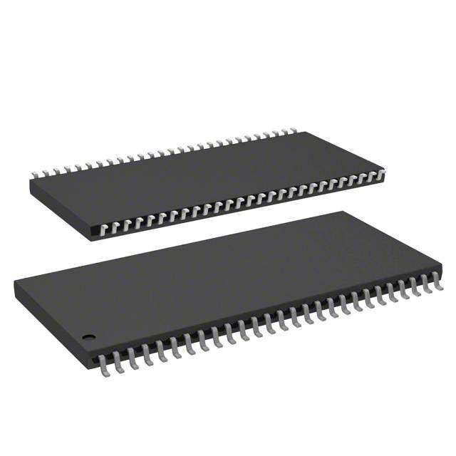
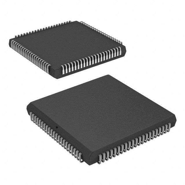
| 供应商器件封装 | 54-TSOP II |
| 其它名称 | 706-1077 |
| 包装 | 托盘 |
| 商标 | ISSI |
| 存储器类型 | SDRAM |
| 存储容量 | 64 Mbit |
| 安装风格 | SMD/SMT |
| 封装 | Tray |
| 封装/外壳 | 54-TSOP(0.400",10.16mm 宽) |
| 封装/箱体 | TSOP-50 |
| 工作温度 | 0°C ~ 70°C |
| 工厂包装数量 | 108 |
| 接口 | 并联 |
| 数据总线宽度 | 16 bit |
| 最大工作温度 | + 70 C |
| 最大工作电流 | 100 mA |
| 最大时钟频率 | 143 MHz |
| 最小工作温度 | 0 C |
| 标准包装 | 108 |
| 格式-存储器 | RAM |
| 电压-电源 | 3 V ~ 3.6 V |
| 电源电压-最大 | 3.6 V |
| 电源电压-最小 | 3 V |
| 类型 | SDRAM |
| 系列 | IS42S16400F |
| 组织 | 4 M x 16 |
| 访问时间 | 5.4 ns |
| 速度 | 143MHz |

%20Renders/54-TSOP.jpg)

_renders/IS66WVE4M16EBLL-70BLI.jpg)


- 商务部:美国ITC正式对集成电路等产品启动337调查
- 曝三星4nm工艺存在良率问题 高通将骁龙8 Gen1或转产台积电
- 太阳诱电将投资9.5亿元在常州建新厂生产MLCC 预计2023年完工
- 英特尔发布欧洲新工厂建设计划 深化IDM 2.0 战略
- 台积电先进制程称霸业界 有大客户加持明年业绩稳了
- 达到5530亿美元!SIA预计今年全球半导体销售额将创下新高
- 英特尔拟将自动驾驶子公司Mobileye上市 估值或超500亿美元
- 三星加码芯片和SET,合并消费电子和移动部门,撤换高东真等 CEO
- 三星电子宣布重大人事变动 还合并消费电子和移动部门
- 海关总署:前11个月进口集成电路产品价值2.52万亿元 增长14.8%

_renders/IS61WV102416BLL-10TLI.jpg)

_renders/IS45S16320F-7BLA1.jpg)
PDF Datasheet 数据手册内容提取
IS42S16400F IS45S16400F 1 Meg Bits x 16 Bits x 4 Banks (64-MBIT) DECEMBER 2011 SYNCHRONOUS DYNAMIC RAM FEATURES OVERVIEW • Clock frequency: 200, 166, 143, 133 MHz ISSI's 64Mb Synchronous DRAM is organized as 1,048,576 bits x 16-bit x 4-bank for improved performance. The • Fully synchronous; all signals referenced to a synchronous DRAMs achieve high-speed data transfer positive clock edge using pipeline architecture. All inputs and outputs signals • Internal bank for hiding row access/precharge refer to the rising edge of the clock input. • Single 3.3V power supply • LVTTL interface • Programmable burst length – (1, 2, 4, 8, full page) KEY TIMING PARAMETERS • Programmable burst sequence: Parameter -5 -6 -7 Unit Sequential/Interleave Clk Cycle Time • Self refresh modes CAS Latency = 3 5 6 7 ns CAS Latency = 2 7.5 7.5 7.5 ns • Auto refresh (CBR) Clk Frequency • 4096 refresh cycles every 64 ms (Com, Ind, A1 CAS Latency = 3 200 166 143 Mhz grade) or 16ms (A2 grade) CAS Latency = 2 133 133 133 Mhz • Random column address every clock cycle Access Time from Clock • Programmable CAS latency (2, 3 clocks) CAS Latency = 3 5 5.4 5.4 ns CAS Latency = 2 6 6 6 ns • Burst read/write and burst read/single write operations capability • Burst termination by burst stop and precharge command ADDRESS TABLE OPTIONS Parameter 4M x 16 • Package: Configuration 1M x 16 x 4 54-pin TSOP II banks 54-ball FBGA (8mm x 8mm) Refresh Count • Operating Temperature Range Com./Ind. 4K/64ms Commercial (0oC to +70oC) A1 4K/64ms Industrial (-40oC to +85oC) A2 4K/16ms Automotive Grade A1 (-40oC to +85oC) Row Addresses A0-A11 Automotive Grade A2 (-40oC to +105oC) Column Addresses A0-A7 Bank Address Pins BA0, BA1 Auto Precharge Pins A10/AP Copyright © 2011 Integrated Silicon Solution, Inc. All rights reserved. ISSI reserves the right to make changes to this specification and its products at any time without notice. ISSI assumes no liability arising out of the application or use of any information, products or services described herein. Customers are advised to obtain the latest version of this device specification before relying on any published information and before placing orders for products. Integrated Silicon Solution, Inc. does not recommend the use of any of its products in life support applications where the failure or malfunction of the product can reasonably be ex- pected to cause failure of the life support system or to significantly affect its safety or effectiveness. Products are not authorized for use in such applications unless Integrated Silicon Solution, Inc. receives written assurance to its satisfaction, that: a.) the risk of injury or damage has been minimized; b.) the user assume all such risks; and c.) potential liability of Integrated Silicon Solution, Inc is adequately protected under the circumstances Integrated Silicon Solution, Inc. — www.issi.com 1 Rev. I 12/01/2011
IS42S16400F IS45S16400F GENERAL DESCRIPTION The 64Mb SDRAM is a high speed CMOS, dynamic other three banks will hide the precharge cycles and provide random-access memory designed to operate in 3.3V seamless, high-speed, random-access operation. memory systems containing 67,108,864 bits. Internally SDRAM read and write accesses are burst oriented starting configured as a quad-bank DRAM with a synchronous at a selected location and continuing for a programmed interface. Each 16,777,216-bit bank is organized as 4,096 number of locations in a programmed sequence. The rows by 256 columns by 16 bits. registration of an ACTIVE command begins accesses, The 64Mb SDRAM includes an AUTO REFRESH MODE, followed by a READ or WRITE command. The ACTIVE and a power-saving, power-down mode. All signals are command in conjunction with address bits registered are registered on the positive edge of the clock signal, CLK. used to select the bank and row to be accessed (BA0, All inputs and outputs are LVTTL compatible. BA1 select the bank; A0-A11 select the row). The READ The 64Mb SDRAM has the ability to synchronously burst or WRITE commands in conjunction with address bits data at a high data rate with automatic column-address registered are used to select the starting column location generation, the ability to interleave between internal banks for the burst access. to hide precharge time and the capability to randomly Programmable READ or WRITE burst lengths consist of change column addresses on each clock cycle during 1, 2, 4 and 8 locations, or full page, with a burst terminate burst access. option. A self-timed row precharge initiated at the end of the burst sequence is available with the AUTO PRECHARGE function enabled. Precharge one bank while accessing one of the FUNCTIONAL BLOCK DIAGRAM CLK DQM CKE CS COMMAND DATA IN RAS DECODER BUFFER CAS & 16 16 WE CLOCK REFRESH A10 GENERATOR MODE CONTROLLER DQ 0-15 REGISTER 12 SELF DATA OUT VDD/VDDQ A11 REFRESH BUFFER GND/GNDQ CONTROLLER 16 16 A9 A8 A7 REFRESH A6 COUNTER A5 A4 4096 A3 ER 4096 BBAAAAA21001 ADRDORWESS ULTIPLEXER ADRDORWESS 12 ROW DECOD 44009966 MEBMAAORNRRYKA YC 0ELL 12 LATCH M BUFFER 12 SENSE AMP I/O GATE 256K (x 16) COLUMN ADDRESS LATCH BANK CONTROL LOGIC 8 BURST COUNTER COLUMN DECODER COLUMN ADDRESS BUFFER 8 2 Integrated Silicon Solution, Inc. — www.issi.com Rev. I 12/01/2011
IS42S16400F IS45S16400F PIN CONFIGURATION PACKAge Code: B 54 BALL fBgA (Top View) (8 mm x 8 mm Body, 0.8 mm Ball Pitch) 1 2 3 4 5 6 7 8 9 A GND DQ15 GNDQ VDDQ DQ0 VDD B DQ14 DQ13 VDDQ GNDQ DQ2 DQ1 C DQ12 DQ11 GNDQ VDDQ DQ4 DQ3 D DQ10 DQ9 VDDQ GNDQ DQ6 DQ5 E DQ8 NC GND VDD DQML DQ7 F DQMH CLK CKE CAS RAS WE G NC A11 A9 BA0 BA1 CS H A8 A7 A6 A0 A1 A10 J GND A5 A4 A3 A2 VDD PIN DESCRIPTIONS A0-A11 Row Address Input WE Write enable A0-A7 Column Address Input LdQM, UdQM x16 Input/output Mask BA0, BA1 Bank Select Addresses Vdd Power dQ0 to dQ15 data I/o gNd ground CLK System Clock Input Vddq Power Supply for I/o Pin CKe Clock enable gNdQ ground for I/o Pin CS Chip Select NC No Connection RAS Row Address Strobe Command CAS Column Address Strobe Command Integrated Silicon Solution, Inc. — www.issi.com 3 Rev. I 12/01/2011
IS42S16400F IS45S16400F PIN CONFIGURATIONS 54 pin TSOP - Type II VDD 1 54 GND DQ0 2 53 DQ15 VDDQ 3 52 GNDQ DQ1 4 51 DQ14 DQ2 5 50 DQ13 GNDQ 6 49 VDDQ DQ3 7 48 DQ12 DQ4 8 47 DQ11 VDDQ 9 46 GNDQ DQ5 10 45 DQ10 DQ6 11 44 DQ9 GNDQ 12 43 VDDQ DQ7 13 42 DQ8 VDD 14 41 GND LDQM 15 40 NC WE 16 39 UDQM CAS 17 38 CLK RAS 18 37 CKE CS 19 36 NC BA0 20 35 A11 BA1 21 34 A9 A10 22 33 A8 A0 23 32 A7 A1 24 31 A6 A2 25 30 A5 A3 26 29 A4 VDD 27 28 GND PIN DESCRIPTIONS A0-A11 Row Address Input WE Write Enable A0-A7 Column Address Input LDQM x16 Lower Byte, Input/Output Mask BA0, BA1 Bank Select Address UDQM x16 Upper Byte, Input/Output Mask DQ0 to DQ15 Data I/O Vdd Power CLK System Clock Input GND Ground CKE Clock Enable Vddq Power Supply for I/O Pin CS Chip Select GNDq Ground for I/O Pin RAS Row Address Strobe Command NC No Connection CAS Column Address Strobe Command 4 Integrated Silicon Solution, Inc. — www.issi.com Rev. I 12/01/2011
IS42S16400F IS45S16400F PIN FUNCTIONS Symbol TSOP Pin No. Type Function (In Detail) A0-A11 23 to 26 Input Pin Address Inputs: A0-A11 are sampled during the ACTIVE 29 to 34 command (row-address A0-A11) and READ/WRITE command (A0-A7 22, 35 with A10 defining auto precharge) to select one location out of the memory array in the respective bank. A10 is sampled during a PRECHARGE command to deter- mine if all banks are to be precharged (A10 HIGH) or bank selected by BA0, BA1 (LOW). The address inputs also provide the op-code during a LOAD MODE REGISTER command. BA0, BA1 20, 21 Input Pin Bank Select Address: BA0 and BA1 defines which bank the ACTIVE, READ, WRITE or PRECHARGE command is being applied. CAS 17 Input Pin CAS, in conjunction with the RAS and WE, forms the device command. See the "Command Truth Table" for details on device commands. CKE 37 Input Pin The CKE input determines whether the CLK input is enabled. The next rising edge of the CLK signal will be valid when is CKE HIGH and invalid when LOW. When CKE is LOW, the device will be in either power-down mode, clock suspend mode, or self refresh mode. CKE is an asynchronous input. CLK 38 Input Pin CLK is the master clock input for this device. Except for CKE, all inputs to this device are acquired in synchronization with the rising edge of this pin. CS 19 Input Pin The CS input determines whether command input is enabled within the device. Command input is enabled when CS is LOW, and disabled with CS is HIGH. The device remains in the previous state when CS is HIGH. DQ0 to 2, 4, 5, 7, 8, 10, DQ Pin DQ0 to DQ15 are I/O pins. I/O through these pins can be controlled in byte units DQ15 11,13, 42, 44, 45, using the LDQM and UDQM pins. 47, 48, 50, 51, 53 LDQM, 15, 39 Input Pin LDQM and UDQM control the lower and upper bytes of the I/O buffers. In read UDQM mode, LDQM and UDQM control the output buffer. When LDQM or UDQM is LOW, the corresponding buffer byte is enabled, and when HIGH, disabled. The outputs go to the HIGH impedance state when LDQM/UDQM is HIGH. This function cor- responds to OE in conventional DRAMs. In write mode, LDQM and UDQM control the input buffer. When LDQM or UDQM is LOW, the corresponding buffer byte is en- abled, and data can be written to the device. When LDQM or UDQM is HIGH, input data is masked and cannot be written to the device. RAS 18 Input Pin RAS, in conjunction with CAS and WE, forms the device command. See the "Com- mand Truth Table" item for details on device commands. WE 16 Input Pin WE, in conjunction with RAS and CAS, forms the device command. See the "Com- mand Truth Table" item for details on device commands. Vddq 3, 9, 43, 49 Power Supply Pin Vddq is the output buffer power supply. Vdd 1, 14, 27 Power Supply Pin Vdd is the device internal power supply. GNdq 6, 12, 46, 52 Power Supply Pin GNdq is the output buffer ground. GNd 28, 41, 54 Power Supply Pin GNd is the device internal ground. Integrated Silicon Solution, Inc. — www.issi.com 5 Rev. I 12/01/2011
IS42S16400F IS45S16400F READ either enabled or disabled. AUTO PRECHARGE does not apply except in full-page burst mode. Upon completion of The READ command selects the bank from BA0, BA1 inputs the READ or WRITE burst, a precharge of the bank/row and starts a burst read access to an active row. Inputs that is addressed is automatically performed. A0-A7 provides the starting column location. When A10 is HIGH, this command functions as an AUTO PRECHARGE AUTO REFRESH COMMAND command. When the auto precharge is selected, the row This command executes the AUTO REFRESH operation. being accessed will be precharged at the end of the READ The row address and bank to be refreshed are automatically burst. The row will remain open for subsequent accesses generated during this operation. The stipulated period (trc) is when AUTO PRECHARGE is not selected. DQ’s read required for a single refresh operation, and no other com- data is subject to the logic level on the DQM inputs two mands can be executed during this period. This command clocks earlier. When a given DQM signal was registered is executed at least 4096 times every Tref. During an AUTO HIGH, the corresponding DQ’s will be High-Z two clocks REFRESH command, address bits are “Don’t Care”. This later. DQ’s will provide valid data when the DQM signal command corresponds to CBR Auto-refresh. was registered LOW. SELF REFRESH WRITE During the SELF REFRESH operation, the row address to A burst write access to an active row is initiated with the be refreshed, the bank, and the refresh interval are gen- WRITE command. BA0, BA1 inputs selects the bank, erated automatically internally. SELF REFRESH can be and the starting column location is provided by inputs used to retain data in the SDRAM without external clocking, A0-A7. Whether or not AUTO-PRECHARGE is used is even if the rest of the system is powered down. The SELF determined by A10. REFRESH operation is started by dropping the CKE pin The row being accessed will be precharged at the end of from HIGH to LOW. During the SELF REFRESH operation the WRITE burst, if AUTO PRECHARGE is selected. If all other inputs to the SDRAM become “Don’t Care”. The AUTO PRECHARGE is not selected, the row will remain device must remain in self refresh mode for a minimum open for subsequent accesses. period equal to tras or may remain in self refresh mode A memory array is written with corresponding input data for an indefinite period beyond that. The SELF-REFRESH on DQ’s and DQM input logic level appearing at the same operation continues as long as the CKE pin remains LOW time. Data will be written to memory when DQM signal is and there is no need for external control of any other pins. LOW. When DQM is HIGH, the corresponding data inputs The next command cannot be executed until the device will be ignored, and a WRITE will not be executed to that internal recovery period (trc) has elapsed. Once CKE byte/column location. goes HIGH, the NOP command must be issued (minimum of two clocks) to provide time for the completion of any PRECHARGE internal refresh in progress. After the self-refresh, since it The PRECHARGE command is used to deactivate the is impossible to determine the address of the last row to open row in a particular bank or the open row in all banks. be refreshed, an AUTO-REFRESH should immediately be BA0, BA1 can be used to select which bank is precharged performed for all addresses. or they are treated as “Don’t Care”. A10 determines BURST TERMINATE whether one or all banks are precharged. After execut- ing this command, the next command for the selected The BURST TERMINATE command forcibly terminates bank(s) is executed after passage of the period t , which the burst read and write operations by truncating either RP is the period required for bank precharging. Once a bank fixed-length or full-page bursts and the most recently has been precharged, it is in the idle state and must be registered READ or WRITE command prior to the BURST activated prior to any READ or WRITE commands being TERMINATE. issued to that bank. COMMAND INHIBIT AUTO PRECHARGE COMMAND INHIBIT prevents new commands from being The AUTO PRECHARGE function ensures that the executed. Operations in progress are not affected, apart precharge is initiated at the earliest valid stage within a from whether the CLK signal is enabled burst. This function allows for individual-bank precharge NO OPERATION without requiring an explicit command. A10 can be used to enable the AUTO PRECHARGE function in conjunc- When CS is low, the NOP command prevents unwanted tion with a specific READ or WRITE command. For each commands from being registered during idle or wait individual READ or WRITE command, auto precharge is states. 6 Integrated Silicon Solution, Inc. — www.issi.com Rev. I 12/01/2011
IS42S16400F IS45S16400F LOAD MODE REGISTER During the LOAD MODE REGISTER command the mode register is loaded from A0-A11. This command can only be issued when all banks are idle. ACTIVE COMMAND When the ACTIVE COMMAND is activated, BA0, BA1 inputs selects a bank to be accessed, and the address inputs on A0-A11 selects the row. Until a PRECHARGE command is issued to the bank, the row remains open for accesses. Integrated Silicon Solution, Inc. — www.issi.com 7 Rev. I 12/01/2011
IS42S16400F IS45S16400F TRUTH TABLE – COMMANDS AND DQM OPERATION(1) FUNCTION CS RAS CAS WE DQM ADDR DQs COMMAND INHIBIT (NOP) H X X X X X X NO OPERATION (NOP) L H H H X X X ACTIVE (Select bank and activate row)(3) L L H H X Bank/Row X READ (Select bank/column, start READ burst)(4) L H L H L/H(8) Bank/Col X WRITE (Select bank/column, start WRITE burst)(4) L H L L L/H(8) Bank/Col Valid BURST TERMINATE L H H L X X Active PRECHARGE (Deactivate row in bank or banks)(5) L L H L X Code X AUTO REFRESH or SELF REFRESH(6,7) L L L H X X X (Enter self refresh mode) LOAD MODE REGISTER(2) L L L L X Op-Code X Write Enable/Output Enable(8) — — — — L — Active Write Inhibit/Output High-Z(8) — — — — H — High-Z NOTES: 1. CKE is HIGH for all commands except SELF REFRESH. 2. A0-A11 define the op-code written to the mode register. 3. A0-A11 provide row address, and BA0, BA1 determine which bank is made active. 4. A0-A7 (x16) provide column address; A10 HIGH enables the auto precharge feature (nonpersistent), while A10 LOW disables auto precharge; BA0, BA1 determine which bank is being read from or written to. 5. A10 LOW: BA0, BA1 determine the bank being precharged. A10 HIGH: All banks precharged and BA0, BA1 are “Don’t Care.” 6. AUTO REFRESH if CKE is HIGH, SELF REFRESH if CKE is LOW. 7. Internal refresh counter controls row addressing; all inputs and I/Os are “Don’t Care” except for CKE. 8. Activates or deactivates the DQs during WRITEs (zero-clock delay) and READs (two-clock delay). 8 Integrated Silicon Solution, Inc. — www.issi.com Rev. I 12/01/2011
IS42S16400F IS45S16400F TRUTH TABLE – CKE (1-4) CURRENT STATE COMMANDn ACTIONn CKEn-1 CKEn Power-Down X Maintain Power-Down L L Self Refresh X Maintain Self Refresh L L Clock Suspend X Maintain Clock Suspend L L Power-Down(5) COMMAND INHIBIT or NOP Exit Power-Down L H Self Refresh(6) COMMAND INHIBIT or NOP Exit Self Refresh L H Clock Suspend(7) X Exit Clock Suspend L H All Banks Idle COMMAND INHIBIT or NOP Power-Down Entry H L All Banks Idle AUTO REFRESH Self Refresh Entry H L Reading or Writing VALID Clock Suspend Entry H L See TRUTH TABLE – CURRENT STATE BANK n, COMMAND TO BANK n H H NOTES: 1. CKEn is the logic state of CKE at clock edge n; CKEn-1 was the state of CKE at the previous clock edge. 2. Current state is the state of the SDRAM immediately prior to clock edge n. 3. COMMANDn is the command registered at clock edge n, and ACTONn is a result of COMMANDn. 4. All states and sequences not shown are illegal or reserved. 5. Exiting power-down at clock edge n will put the device in the all banks idle state in time for clock edge n+1 (provided that tcks is met). 6. Exiting self refresh at clock edge n will put the device in all banks idle state once txsr is met. COMMAND INHIBIT or NOP commands should be issued on clock edges occurring during the txsr period. A minimum of two NOP commands must be sent during txsr period. 7. After exiting clock suspend at clock edge n, the device will resume operation and recognize the next command at clock edge n+1. TRUTH TABLE – CURRENT STATE BANK n, COMMAND TO BANK n (1-6) CURRENT STATE COMMAND (ACTION) CS RAS CAS WE Any COMMAND INHIBIT (NOP/Continue previous operation) H X X X NO OPERATION (NOP/Continue previous operation) L H H H Idle ACTIVE (Select and activate row) L L H H AUTO REFRESH(7) L L L H LOAD MODE REGISTER(7) L L L L PRECHARGE(11) L L H L Row Active READ (Select column and start READ burst)(10) L H L H WRITE (Select column and start WRITE burst)(10) L H L L PRECHARGE (Deactivate row in bank or banks)(8) L L H L Read READ (Select column and start new READ burst)(10) L H L H (Auto WRITE (Select column and start WRITE burst)(10) L H L L Precharge PRECHARGE (Truncate READ burst, start PRECHARGE)(8) L L H L Disabled) BURST TERMINATE(9) L H H L Write READ (Select column and start READ burst)(10) L H L H (Auto WRITE (Select column and start new WRITE burst)(10) L H L L Precharge PRECHARGE (Truncate WRITE burst, start PRECHARGE)(8) L L H L Disabled) BURST TERMINATE(9) L H H L NOTE: 1. This table applies when CKE n-1 was HIGH and CKE n is HIGH (see Truth Table - CKE) and after txsr has been met (if the previous state was SELF REFRESH). 2. This table is bank-specific, except where noted; i.e., the current state is for a specific bank and the commands shown are those allowed to be issued to that bank when in that state. Exceptions are covered in the notes below. Integrated Silicon Solution, Inc. — www.issi.com 9 Rev. I 12/01/2011
IS42S16400F IS45S16400F 3. Current state definitions: Idle: The bank has been precharged, and trp has been met. Row Active: A row in the bank has been activated, and trcd has been met. No data bursts/accesses and no register accesses are in progress. Read: A READ burst has been initiated, with auto precharge disabled, and has not yet terminated or been termi- nated. Write: A WRITE burst has been initiated, with auto precharge disabled, and has not yet terminated or been termi- nated. 4. The following states must not be interrupted by a command issued to the same bank. COMMAND INHIBIT or NOP commands, or allowable commands to the other bank should be issued on any clock edge occurring during these states. Allowable com- mands to the other bank are determined by its current state and CURRENT STATE BANK n truth tables. Precharging: Starts with registration of a PRECHARGE command and ends when trp is met. Once trp is met, the bank will be in the idle state. Row Activating: Starts with registration of an ACTIVE command and ends when trcd is met. Once trcd is met, the bank will be in the row active state. Read w/Auto Precharge Enabled: Starts with registration of a READ command with auto precharge enabled and ends when trp has been met. Once trp is met, the bank will be in the idle state. Write w/Auto Precharge Enabled: Starts with registration of a WRITE command with auto precharge enabled and ends when trp has been met. Once trp is met, the bank will be in the idle state. 5. The following states must not be interrupted by any executable command; COMMAND INHIBIT or NOP commands must be applied on each positive clock edge during these states. Refreshing: Starts with registration of an AUTO REFRESH command and ends when trc is met. Once trc is met, the SDRAM will be in the all banks idle state. Accessing Mode Register: Starts with registration of a LOAD MODE REGISTER command and ends when tmrd has been met. Once tmrd is met, the SDRAM will be in the all banks idle state. Precharging All: Starts with registration of a PRECHARGE ALL command and ends when trp is met. Once trp is met, all banks will be in the idle state. 6. All states and sequences not shown are illegal or reserved. 7. Not bank-specific; requires that all banks are idle. 8. May or may not be bank-specific; if all banks are to be precharged, all must be in a valid state for precharging. 9. Not bank-specific; BURST TERMINATE affects the most recent READ or WRITE burst, regardless of bank. 10. READs or WRITEs listed in the Command (Action) column include READs or WRITEs with auto precharge enabled and READs or WRITEs with auto precharge disabled. 11. Does not affect the state of the bank and acts as a NOP to that bank. 10 Integrated Silicon Solution, Inc. — www.issi.com Rev. I 12/01/2011
IS42S16400F IS45S16400F TRUTH TABLE – CURRENT STATE BANK n, COMMAND TO BANK m (1-6) CURRENT STATE COMMAND (ACTION) CS RAS CAS WE Any COMMAND INHIBIT (NOP/Continue previous operation) H X X X NO OPERATION (NOP/Continue previous operation) L H H H Idle Any Command Otherwise Allowed to Bank m X X X X Row ACTIVE (Select and activate row) L L H H Activating, READ (Select column and start READ burst)(7) L H L H Active, or WRITE (Select column and start WRITE burst)(7) L H L L Precharging PRECHARGE L L H L Read ACTIVE (Select and activate row) L L H H (Auto READ (Select column and start new READ burst)(7,10) L H L H Precharge WRITE (Select column and start WRITE burst)(7,11) L H L L Disabled) PRECHARGE(9) L L H L Write ACTIVE (Select and activate row) L L H H (Auto READ (Select column and start READ burst)(7,12) L H L H Precharge WRITE (Select column and start new WRITE burst)(7,13) L H L L Disabled) PRECHARGE(9) L L H L Read ACTIVE (Select and activate row) L L H H (With Auto READ (Select column and start new READ burst)(7,8,14) L H L H Precharge) WRITE (Select column and start WRITE burst)(7,8,15) L H L L PRECHARGE(9) L L H L Write ACTIVE (Select and activate row) L L H H (With Auto READ (Select column and start READ burst)(7,8,16) L H L H Precharge) WRITE (Select column and start new WRITE burst)(7,8,17) L H L L PRECHARGE(9) L L H L NOTE: 1. This table applies when CKE n-1 was HIGH and CKE n is HIGH (Truth Table - CKE) and after txsr has been met (if the previ- ous state was self refresh). 2. This table describes alternate bank operation, except where noted; i.e., the current state is for bank n and the commands shown are those allowed to be issued to bank m (assuming that bank m is in such a state that the given command is allowable). Excep- tions are covered in the notes below. 3. Current state definitions: Idle: The bank has been precharged, and trp has been met. Row Active: A row in the bank has been activated, and trcd has been met. No data bursts/accesses and no register accesses are in progress. Read: A READ burst has been initiated, with auto precharge disabled, and has not yet terminated or been termi- nated. Write: A WRITE burst has been initiated, with auto precharge disabled, and has not yet terminated or been termi- nated. Read w/Auto Precharge Enabled: Starts with registration of a READ command with auto precharge enabled, and ends when trp has been met. Once trp is met, the bank will be in the idle state. Write w/Auto Precharge Enabled: Starts with registration of a WRITE command with auto precharge enabled, and ends when trp has been met. Once trp is met, the bank will be in the idle state. 4. AUTO REFRESH, SELF REFRESH and LOAD MODE REGISTER commands may only be issued when all banks are idle. 5. A BURST TERMINATE command cannot be issued to another bank; it applies to the bank represented by the current state only. 6. All states and sequences not shown are illegal or reserved. 7. READs or WRITEs to bank m listed in the Command (Action) column include READs or WRITEs with auto precharge enabled and READs or WRITEs with auto precharge disabled. Integrated Silicon Solution, Inc. — www.issi.com 11 Rev. I 12/01/2011
IS42S16400F IS45S16400F 8. CONCURRENT AUTO PRECHARGE: Bank n will initiate the AUTO PRECHARGE command when its burst has been inter- rupted by bank m’s burst. 9. Burst in bank n continues as initiated. 10. For a READ without auto precharge interrupted by a READ (with or without auto precharge), the READ to bank m will interrupt the READ on bank n, CAS latency later (Consecutive READ Bursts). 11. For a READ without auto precharge interrupted by a WRITE (with or without auto precharge), the WRITE to bank m will inter- rupt the READ on bank n when registered (READ to WRITE). DQM should be used one clock prior to the WRITE command to prevent bus contention. 12. For a WRITE without auto precharge interrupted by a READ (with or without auto precharge), the READ to bank m will interrupt the WRITE on bank n when registered (WRITE to READ), with the data-out appearing CAS latency later. The last valid WRITE to bank n will be data-in registered one clock prior to the READ to bank m. 13. For a WRITE without auto precharge interrupted by a WRITE (with or without auto precharge), the WRITE to bank m will inter- rupt the WRITE on bank n when registered (WRITE to WRITE). The last valid WRITE to bank n will be data-in registered one clock prior to the READ to bank m. 14. For a READ with auto precharge interrupted by a READ (with or without auto precharge), the READ to bank m will interrupt the READ on bank n, CAS latency later. The PRECHARGE to bank n will begin when the READ to bank m is registered (Fig CAP 1). 15. For a READ with auto precharge interrupted by a WRITE (with or without auto precharge), the WRITE to bank m will interrupt the READ on bank n when registered. DQM should be used two clocks prior to the WRITE command to prevent bus contention. The PRECHARGE to bank n will begin when the WRITE to bank m is registered (Fig CAP 2). 16. For a WRITE with auto precharge interrupted by a READ (with or without auto precharge), the READ to bank m will interrupt the WRITE on bank n when registered, with the data-out appearing CAS latency later. The PRECHARGE to bank n will begin after tWR is met, where twr begins when the READ to bank m is registered. The last valid WRITE to bank n will be data-in regis- tered one clock prior to the READ to bank m (Fig CAP 3). 17. For a WRITE with auto precharge interrupted by a WRITE (with or without auto precharge), the WRITE to bank m will interrupt the WRITE on bank n when registered. The PRECHARGE to bank n will begin after twr is met, where t WR begins when the WRITE to bank m is registered. The last valid WRITE to bank n will be data registered one clock prior to the WRITE to bank m (Fig CAP 4). 12 Integrated Silicon Solution, Inc. — www.issi.com Rev. I 12/01/2011
IS42S16400F IS45S16400F ABSOLUTE MAXIMUM RATINGS(1) Symbol Parameters Rating Unit Vdd max Maximum Supply Voltage –1.0 to +4.6 V Vddq max Maximum Supply Voltage for Output Buffer –1.0 to +4.6 V ViN Input Voltage –1.0 to Vddq + 0.5 V Vout Output Voltage –1.0 to Vddq + 0.5 V Pd max Allowable Power Dissipation 1 W Ics output Shorted Current 50 mA Topr operating Temperature Com. 0 to +70 °C Ind. -40 to +85 °C A1 -40 to +85 °C A2 -40 to +105 °C Tstg Storage Temperature –65 to +150 °C DC RECOMMENDED OPERATING CONDITIONS(2) (At Ta = 0 to +70°C for commercial grade. Ta = -40 to +85°C for industrial and A1 grade. Ta = -40 to +105°C for A2 grade) Symbol Parameter Min. Typ. Max. Unit Vdd, Vddq Supply Voltage 3.0 3.3 3.6 V Vih Input High Voltage(3) 2.0 — Vdd + 0.3 V Vil Input Low Voltage(4) -0.3 — +0.8 V CAPACITANCE CHARACTERISTICS(1,2) (At Ta = 0 to +25°C, Vdd = Vddq = 3.3 ± 0.3V, f = 1 MHz) Symbol Parameter Typ. Max. Unit CiN Input Capacitance: Address and Control — 3.8 pF Cclk Input Capacitance: (CLK) — 3.5 pF CI/O Data Input/Output Capacitance: I/O0-I/O15 — 6.5 pF Notes: 1. Stress greater than those listed under ABSOLUTE MAXIMUM RATINGS may cause permanent damage to the device. This is a stress rating only and functional operation of the device at these or any other conditions above those indicated in the operational sections of this specification is not implied. Exposure to absolute maximum rating conditions for extended periods may affect reliability. 2. All voltages are referenced to GND. 3. Vih(max) = Vddq + 1.2V with a pulse width < 3ns. 4. Vil(min) = GND - 1.2V with a pulse width < 3ns. 5. This parameter is characterized. Integrated Silicon Solution, Inc. — www.issi.com 13 Rev. I 12/01/2011
IS42S16400F IS45S16400F DC ELECTRICAL CHARACTERISTICS (Recommended Operation Conditions unless otherwise noted.) Symbol Parameter Test Condition Speed Min. Max. Unit iil Input Leakage Current 0V ≤ ViN ≤ Vdd, with pins other than –5 5 µA the tested pin at 0V iol Output Leakage Current Output is disabled, 0V ≤ Vout ≤ Vdd –5 5 µA Voh Output High Voltage Level iout = –2 mA 2.4 — V Vol Output Low Voltage Level iout = +2 mA — 0.4 V icc1 Operating Current(1,2) One Bank Operation, CAS latency = 3 Com. -5 — 110 mA Burst Length=1 Com. -6 — 95 mA trc ≥ trc (min.) Com. -7 — 85 mA Iout = 0mA A1, Ind. -5/-6 — 155 mA A1, A2, Ind. -7 — 145 mA icc2p Precharge Standby Current CKE ≤ Vil (max) tck = 15ns Com. — — 2 mA A1, A2, Ind. — — 4 mA Icc2ps (In Power-Down Mode) tck = ∞ Com. — — 2 mA A1, A2, Ind. — — 3 mA icc2N(3) Precharge Standby Current CKE ≥ Vih (miN) tck = 15ns — — 20 mA Icc2Ns (In Non Power-Down Mode) tck = ∞ Com. — — 15 mA A1, A2, Ind. — — 15 mA icc3p Active Standby Current CKE ≤ Vil (max) tck = 15ns Com. — — 7 mA A1, A2, Ind. — — 7 mA icc3ps (In Power-Down Mode) tck = ∞ Com. — — 5 mA A1, A2, Ind. — — 5 mA icc3N(3) Active Standby Current CKE ≥ Vih (miN) tck = 15ns — — 30 mA Icc3Ns (In Non Power-Down Mode) tck = ∞ Com. — — 25 mA A1, A2, Ind. — — 25 mA icc4 Operating Current tck = tck (miN) CAS latency = 3 Com. -5 — 140 mA (In Burst Mode)(1) Iout = 0mA Com. -6 — 130 mA BL = 4; 4 banks activated Com. -7 — 100 mA A1, Ind. -5/-6 — 140 mA A1, A2, Ind. -7 — 110 mA icc5 Auto-Refresh Current trc = trc (miN) CAS latency = 3 Com. -5 — 160 mA tclk = tclk (miN) Com. -6 — 150 mA Com. -7 — 130 mA A1, Ind. -5/-6 — 170 mA A1, A2, Ind. -7 — 150 mA icc6 Self-Refresh Current CKE ≤ 0.2V — — 2 mA Notes: 1. These are the values at the minimum cycle time. Since the currents are transient, these values decrease as the cycle time in- creases. Also note that a bypass capacitor of at least 0.01 µF should be inserted between Vdd and GND for each memory chip to suppress power supply voltage noise (voltage drops) due to these transient currents. 2. Icc1 and Icc4 depend on the output load. The maximum values for Icc1 and Icc4 are obtained with the output open state. 3. Input signal chnage once per 30ns. 14 Integrated Silicon Solution, Inc. — www.issi.com Rev. I 12/01/2011
IS42S16400F IS45S16400F AC ELECTRICAL CHARACTERISTICS (1,2,3) -5 -6 -7 Symbol Parameter Min. Max. Min. Max. Min. Max. Units tck3 Clock Cycle Time CAS Latency = 3 5 — 6 — 7 — ns tck2 CAS Latency = 2 7.5 — 7.5 — 7.5 — ns tac3 Access Time From CLK(4,6) CAS Latency = 3 — 5 — 5.4 — 5.4 ns tac2 CAS Latency = 2 — 6 — 6 — 6 ns tch CLK HIGH Level Width 2 — 2 — 2.5 — ns tcl CLK LOW Level Width 2 — 2 — 2.5 — ns toh3 Output Data Hold Time(6) CAS Latency = 3 2.5 — 2.5 — 2.7 — ns toh2 CAS Latency = 2 2.5 — 2.5 — 2.7 — ns tlz Output LOW Impedance Time 0 — 0 — 0 — ns thz3 Output HIGH Impedance Time(5) CAS Latency = 3 — 5 — 5.4 — 5.4 ns thz2 CAS Latency = 2 — 6 — 6 — 6 ns tds Input Data Setup Time 1.5 — 1.5 — 1.5 — ns tdh Input Data Hold Time 0.8 — 0.8 — 0.8 — ns tas Address Setup Time 1.5 — 1.5 — 1.5 — ns tah Address Hold Time 0.8 — 0.8 — 0.8 — ns tcks CKE Setup Time 1.5 — 1.5 — 1.5 — ns tckh CKE Hold Time 0.8 — 0.8 — 0.8 — ns tcka CKE to CLK Recovery Delay Time 1CLK+3 — 1CLK+3 — 1CLK+3 — ns tcms Command Setup Time (CS, RAS, CAS, WE, DQM) 1.5 — 1.5 — 1.5 — ns tcmh Command Hold Time (CS, RAS, CAS, WE, DQM) 0.8 — 0.8 — 0.8 — ns trc Command Period (REF to REF / ACT to ACT) 55 — 60 — 63 — ns tras Command Period (ACT to PRE) 40 100,000 42 100,000 42 100,000 ns trp Command Period (PRE to ACT) 15 — 18 — 20 — ns trcd Active Command To Read / Write Command Delay Time 15 — 18 — 20 — ns trrd Command Period (ACT [0] to ACT[1]) 10 — 12 — 14 — ns tdpl or Input Data To Precharge CAS Latency = 3 2CLK — 2CLK — 2CLK — ns twr Command Delay time CAS Latency = 2 2CLK — 2CLK — 2CLK — ns tdal Input Data To Active / Refresh CAS Latency = 3 2CLK+trp — 2CLK+trp — 2CLK+trp — ns Command Delay time (During Auto-Precharge) CAS Latency = 2 2CLK+trp — 2CLK+trp — 2CLK+trp — ns tt Transition Time 0.3 1.2 0.3 1.2 0.3 1.2 ns txsr Exit to Self-Refresh to Active Time 60 — 66 — 70 — ns tref Refresh Cycle Time (4096) Ta ≤ 70oC Com., Ind., A1, A2 — 64 — 64 — 64 ms Ta ≤ 85oC Ind., A1, A2 — 64 — 64 — 64 ms Ta > 85oC A2 — — — — — 16 ms Notes: 1. When power is first applied, memory operation should be started 200 µs after Vdd and Vddq reach their stipulated voltages. Also note that the power-on sequence must be executed before starting memory operation. 2. measured with tt = 1 ns. 3. The reference level is 1.4 V when measuring input signal timing. Rise and fall times are measured between Vih (min.) and Vil (max.). 4. Access time is measured at 1.4V with the load shown in the figure below. 5. The time thz (max.) is defined as the time required for the output voltage to transition by ± 200 mV from Voh (min.) or Vol (max.) when the output is in the high impedance state. 6. If clock rising time is longer than 1ns, tt/2 - 0.5ns should be added to the parameter. Integrated Silicon Solution, Inc. — www.issi.com 15 Rev. I 12/01/2011
IS42S16400F IS45S16400F OPERATING FREQUENCY / LATENCY RELATIONSHIPS SYMBOL PARAMETER -5 -6 -7 UNITS — Clock Cycle Time CL=3 5 6 7 ns CL=2 7.5 7.5 7.5 ns — Operating Frequency CL=3 200 166 143 MHz CL=2 133 133 133 MH tccd READ/WRITE command to READ/WRITE command 1 1 1 cycle tcked CKE to clock disable or power-down entry mode 1 1 1 cycle tped CKE to clock enable or power-down exit setup mode 1 1 1 cycle tdqd DQM to input data delay 0 0 0 cycle tdqm DQM to data mask during WRITEs 0 0 0 cycle tdqz DQM to data high-impedance during READs 2 2 2 cycle tdwd WRITE command to input data delay 0 0 0 cycle tdal Data-in to ACTIVE command CL=3 5 5 5 cycle CL=2 4 5 5 cycle tdpl Data-in to PRECHARGE command 2 2 2 cycle tbdl Last data-in to burst STOP command 1 1 1 cycle tcdl Last data-in to new READ/WRITE command 1 1 1 cycle trdl Last data-in to PRECHARGE command 2 2 2 cycle tmrd LOAD MODE REGISTER command 2 2 2 cycle to ACTIVE or REFRESH command troh Data-out to high-impedance from CL=3 3 3 3 cycle PRECHARGE command CL=2 2 2 2 cycle AC TEST CONDITIONS (Input/Output Reference Level: 1.4V) Input Load Output Load tCK tCH tCL 3.0V 50 Ω CLK 1.4V I/O +1.4V 0V tCMS tCMH 3.0V 50 pF INPUT 1.4V 0V tAC tOH OUTPUT 1.4V 1.4V 16 Integrated Silicon Solution, Inc. — www.issi.com Rev. I 12/01/2011
IS42S16400F IS45S16400F FUNCTIONAL DESCRIPTION Initialization The 64Mb SDRAMs (1 Meg x 16 x 4 banks) are quad-bank SDRAMs must be powered up and initialized in a DRAMs which operate at 3.3V and include a synchronous predefined manner. interface (all signals are registered on the positive edge of The 64Mb SDRAM is initialized after the power is applied the clock signal, CLK). Each of the 16,777,216-bit banks is to Vdd and Vddq (simultaneously), and the clock is stable organized as 4,096 rows by 256 columns by 16 bits. with DQM High and CKE High. Read and write accesses to the SDRAM are burst oriented; A 100µs delay is required prior to issuing any command accesses start at a selected location and continue for other than a COMMAND INHIBIT or a NOP. The COMMAND a programmed number of locations in a programmed INHIBIT or NOP may be applied during the 100µs period and sequence. Accesses begin with the registration of an AC- continue should at least through the end of the period. TIVE command which is then followed by a READ or WRITE With at least one COMMAND INHIBIT or NOP command command. The address bits registered coincident with the having been applied, a PRECHARGE command should ACTIVE command are used to select the bank and row to be applied once the 100µs delay has been satisfied. All be accessed (BA0 and BA1 select the bank, A0-A11 select the banks must be precharged. This will leave all banks in row). The address bits (A0-A7) registered coincident with the an idle state, after which at least two AUTO REFRESH cycles READ or WRITE command are used to select the starting must be performed. After the AUTO REFRESH cycles are column location for the burst access. complete, the SDRAM is then ready for mode register Prior to normal operation, the SDRAM must be initial- programming. ized. The following sections provide detailed information The mode register should be loaded prior to applying covering device initialization, register definition, command any operational command because it will power up in an descriptions and device operation. unknown state. After the Load Mode Register command, at least one NOP command must be asserted prior to any command. Integrated Silicon Solution, Inc. — www.issi.com 17 Rev. I 12/01/2011
IS42S16400F IS45S16400F REGISTER DEFINITION Mode Register The mode register is used to define the specific mode Mode register bits M0-M2 specify the burst length, M3 of operation of the SDRAM. This definition includes the specifies the type of burst (sequential or interleaved), M4- M6 selection of a burst length, a burst type, a CAS latency, specify the CAS latency, M7 and M8 specify the operating an operating mode and a write burst mode, as shown in mode, M9 specifies the WRITE burst mode, and M10 and MODE REGISTER DEFINITION. M11 are reserved for future use. The mode register is programmed via the LOAD MODE The mode register must be loaded when all banks are REGISTER command and will retain the stored information idle, and the controller must wait the specified time before until it is programmed again or the device loses power. initiating the subsequent operation. Violating either of these requirements will result in unspecified operation. MODE REGISTER DEFINITION A11 A10 A9 A8 A7 A6 A5 A4 A3 A2 A1 A0 Address Bus Mode Register (Mx) Reserved(1) Burst Length M2 M1 M0 M3=0 M3=1 0 0 0 1 1 0 0 1 2 2 0 1 0 4 4 0 1 1 8 8 1 0 0 Reserved Reserved 1 0 1 Reserved Reserved 1 1 0 Reserved Reserved 1 1 1 Full Page Reserved Burst Type M3 Type 0 Sequential 1 Interleaved Latency Mode M6 M5 M4 CAS Latency 0 0 0 Reserved 0 0 1 Reserved 0 1 0 2 0 1 1 3 1 0 0 Reserved 1 0 1 Reserved 1 1 0 Reserved 1 1 1 Reserved Operating Mode M8 M7 M6-M0 Mode 0 0 Defined Standard Operation — — — All Other States Reserved Write Burst Mode M9 Mode 0 Programmed Burst Length 1. To ensure compatibility with future devices, 1 Single Location Access should program M11, M10 = "0, 0" 18 Integrated Silicon Solution, Inc. — www.issi.com Rev. I 12/01/2011
IS42S16400F IS45S16400F Burst Length Read and write accesses to the SDRAM are burst oriented, ing that the burst will wrap within the block if a boundary with the burst length being programmable, as shown in is reached. The block is uniquely selected by A1-A7 (x16) MODE REGISTER DEFINITION. The burst length deter- when the burst length is set to two; by A2-A7 (x16) when mines the maximum number of column locations that can the burst length is set to four; and by A3-A7 (x16) when the be accessed for a given READ or WRITE command. Burst burst length is set to eight. The remaining (least significant) lengths of 1, 2, 4 or 8 locations are available for both the address bit(s) is (are) used to select the starting location sequential and the interleaved burst types, and a full-page within the block. Full-page bursts wrap within the page if burst is available for the sequential type. The full-page the boundary is reached. burst is used in conjunction with the BURST TERMINATE Burst Type command to generate arbitrary burst lengths. Accesses within a given burst may be programmed to be Reserved states should not be used, as unknown operation either sequential or interleaved; this is referred to as the or incompatibility with future versions may result. burst type and is selected via bit M3. When a READ or WRITE command is issued, a block of The ordering of accesses within a burst is determined by columns equal to the burst length is effectively selected. All the burst length, the burst type and the starting column accesses for that burst take place within this block, mean- address, as shown in BURST DEFINITION table. BURST DEFINITION Burst Starting Column Order of Accesses Within a Burst Length Address Type = Sequential Type = Interleaved A0 2 0 0-1 0-1 1 1-0 1-0 A1 A0 0 0 0-1-2-3 0-1-2-3 4 0 1 1-2-3-0 1-0-3-2 1 0 2-3-0-1 2-3-0-1 1 1 3-0-1-2 3-2-1-0 A2 A1 A0 0 0 0 0-1-2-3-4-5-6-7 0-1-2-3-4-5-6-7 0 0 1 1-2-3-4-5-6-7-0 1-0-3-2-5-4-7-6 0 1 0 2-3-4-5-6-7-0-1 2-3-0-1-6-7-4-5 8 0 1 1 3-4-5-6-7-0-1-2 3-2-1-0-7-6-5-4 1 0 0 4-5-6-7-0-1-2-3 4-5-6-7-0-1-2-3 1 0 1 5-6-7-0-1-2-3-4 5-4-7-6-1-0-3-2 1 1 0 6-7-0-1-2-3-4-5 6-7-4-5-2-3-0-1 1 1 1 7-0-1-2-3-4-5-6 7-6-5-4-3-2-1-0 Full n = A0-A7 Cn, Cn + 1, Cn + 2 Not Supported Page Cn + 3, Cn + 4... (y) (location 0-y) …Cn - 1, Cn… Integrated Silicon Solution, Inc. — www.issi.com 19 Rev. I 12/01/2011
IS42S16400F IS45S16400F CAS Latency Operating Mode The CAS latency is the delay, in clock cycles, between The normal operating mode is selected by setting M7 and M8 the registration of a READ command and the availability of to zero; the other combinations of values for M7 and M8 are the first piece of output data. The latency can be set to two or reserved for future use and/or test modes. The programmed three clocks. burst length applies to both READ and WRITE bursts. If a READ command is registered at clock edge n, and Test modes and reserved states should not be used be- the latency is m clocks, the data will be available by clock cause unknown operation or incompatibility with future edge n + m. The DQs will start driving as a result of the versions may result. clock edge one cycle earlier (n + m - 1), and provided that Write Burst Mode the relevant access times are met, the data will be valid by clock edge n + m. For example, assuming that the clock When M9 = 0, the burst length programmed via M0-M2 cycle time is such that all relevant access times are met, applies to both READ and WRITE bursts; when M9 = 1, if a READ command is registered at T0 and the latency the programmed burst length applies to READ bursts, but is programmed to two clocks, the DQs will start driving write accesses are single-location (nonburst) accesses. after T1 and the data will be valid by T2, as shown in CAS CAS Latency Latency diagrams. The Allowable Operating Frequency table indicates the operating frequencies at which each Allowable Operating Frequency (MHz) CAS latency setting can be used. Speed CAS Latency = 2 CAS Latency = 3 Reserved states should not be used as unknown operation 5 133 200 or incompatibility with future versions may result. 6 133 166 7 133 143 CAS Latency T0 T1 T2 T3 CLK COMMAND READ NOP NOP tAC DQ DOUT tLZ tOH CAS Latency - 2 T0 T1 T2 T3 T4 CLK COMMAND READ NOP NOP NOP tAC DQ DOUT tLZ tOH CAS Latency - 3 DON'T CARE UNDEFINED 20 Integrated Silicon Solution, Inc. — www.issi.com Rev. I 12/01/2011
IS42S16400F IS45S16400F OPERATION Activating Specific Row Within Specific Bank BANK/ROW ACTIVATION Before any READ or WRITE commands can be issued to a bank within the SDRAM, a row in that bank must be CLK “opened.” This is accomplished via the ACTIVE command, which selects both the bank and the row to be activated HIGH CKE (see Activating Specific Row Within Specific Bank). After opening a row (issuing an ACTIVE command), a READ CS or WRITE command may be issued to that row, subject to the trcd specification. Minimum trcd should be divided by RAS the clock period and rounded up to the next whole number to determine the earliest clock edge after the ACTIVE command on which a READ or WRITE command can be CAS entered. For example, a trcd specification of 20ns with a 125 MHz clock (8ns period) results in 2.5 clocks, rounded WE to 3. This is reflected in the following example, which cov- ers any case where 2 < [trcd (MIN)/tck] ≤ 3. (The same procedure is used to convert other specification limits from A0-A11 ROW ADDRESS time units to clock cycles). BA0, BA1 BANK ADDRESS A subsequent ACTIVE command to a different row in the same bank can only be issued after the previous active row has been “closed” (precharged). The minimum time interval between successive ACTIVE commands to the same bank is defined by trc. A subsequent ACTIVE command to another bank can be issued while the first bank is being accessed, which results in a reduction of total row-access overhead. The minimum time interval between successive ACTIVE commands to different banks is defined by trrd. Example: Meeting tRCD (MIN) when 2 < [tRCD (min)/tCK] ≤ 3 T0 T1 T2 T3 T4 CLK COMMAND ACTIVE NOP NOP READ or WRITE tRCD DON'T CARE Integrated Silicon Solution, Inc. — www.issi.com 21 Rev. I 12/01/2011
IS42S16400F IS45S16400F READS READ COMMAND READ bursts are initiated with a READ command, as shown in the READ COMMAND diagram. CLK The starting column and bank addresses are provided with the READ command, and auto precharge is either enabled or HIGH CKE disabled for that burst access. If auto precharge is enabled, the row being accessed is precharged at the completion of CS the burst. For the generic READ commands used in the fol- lowing illustrations, auto precharge is disabled. RAS During READ bursts, the valid data-out element from the starting column address will be available following the CAS latency after the READ command. Each subsequent CAS data-out element will be valid by the next positive clock edge. The CAS Latency diagram shows general timing WE for each possible CAS latency setting. Upon completion of a burst, assuming no other commands A0-A7 COLUMN ADDRESS have been initiated, the DQs will go High-Z. A full-page burst will continue until terminated. (At the end of the page, it will A8, A9, A11 wrap to column 0 and continue.) AUTO PRECHARGE Data from any READ burst may be truncated with a sub- A10 sequent READ command, and data from a fixed-length NO PRECHARGE READ burst may be immediately followed by data from a BA0, BA1 BANK ADDRESS READ command. In either case, a continuous flow of data can be maintained. The first data element from the new burst follows either the last element of a completed burst or the last desired data element of a longer burst which is being truncated. The new READ command should be issued x cycles before The DQM input is used to avoid I/O contention, as shown the clock edge at which the last desired data element is in Figures RW1 and RW2. The DQM signal must be as- valid, where x equals the CAS latency minus one. This is serted (HIGH) at least three clocks prior to the WRITE shown in Consecutive READ Bursts for CAS latencies of command (DQM latency is two clocks for output buffers) two and three; data element n + 3 is either the last of a to suppress data-out from the READ. Once the WRITE burst of four or the last desired of a longer burst. The 64Mb command is registered, the DQs will go High-Z (or remain SDRAM uses a pipelined architecture and therefore does High-Z), regardless of the state of the DQM signal, provided not require the 2n rule associated with a prefetch architec- the DQM was active on the clock just prior to the WRITE ture. A READ command can be initiated on any clock cycle command that truncated the READ command. If not, the following a previous READ command. Full-speed random second WRITE will be an invalid WRITE. For example, if read accesses can be performed to the same bank, as DQM was LOW during T4 in Figure RW2, then the WRITEs shown in Random READ Accesses, or each subsequent at T5 and T7 would be valid, while the WRITE at T6 would READ may be performed to a different bank. be invalid. Data from any READ burst may be truncated with a sub- The DQM signal must be de-asserted prior to the WRITE sequent WRITE command, and data from a fixed-length command (DQM latency is zero clocks for input buffers) READ burst may be immediately followed by data from a to ensure that the written data is not masked. WRITE command (subject to bus turnaround limitations). A fixed-length READ burst may be followed by, or truncated The WRITE burst may be initiated on the clock edge im- with, a PRECHARGE command to the same bank (provided mediately following the last (or last desired) data element that auto precharge was not activated), and a full-page burst from the READ burst, provided that I/O contention can be may be truncated with a PRECHARGE command to the avoided. In a given system design, there may be a pos- same bank. The PRECHARGE command should be issued sibility that the device driving the input data will go Low-Z x cycles before the clock edge at which the last desired before the SDRAM DQs go High-Z. In this case, at least data element is valid, where x equals the CAS latency a single-cycle delay should occur between the last read minus one. This is shown in the READ to PRECHARGE data and the WRITE command. 22 Integrated Silicon Solution, Inc. — www.issi.com Rev. I 12/01/2011
IS42S16400F IS45S16400F diagram for each possible CAS latency; data element n + Full-page READ bursts can be truncated with the BURST 3 is either the last of a burst of four or the last desired of TERMINATE command, and fixed-length READ bursts a longer burst. Following the PRECHARGE command, a may be truncated with a BURST TERMINATE command, subsequent command to the same bank cannot be issued provided that auto precharge was not activated. The BURST until trp is met. Note that part of the row precharge time is TERMINATE command should be issued x cycles before hidden during the access of the last data element(s). the clock edge at which the last desired data element is In the case of a fixed-length burst being executed to valid, where x equals the CAS latency minus one. This is completion, a PRECHARGE command issued at the shown in the READ Burst Termination diagram for each optimum time (as described above) provides the same possible CAS latency; data element n + 3 is the last desired operation that would result from the same fixed-length data element of a longer burst. burst with auto precharge. The disadvantage of the PRE- CHARGE command is that it requires that the command and address buses be available at the appropriate time to issue the command; the advantage of the PRECHARGE command is that it can be used to truncate fixed-length or full-page bursts. CAS Latency T0 T1 T2 T3 CLK COMMAND READ NOP NOP tAC DQ DOUT tLZ tOH CAS Latency - 2 T0 T1 T2 T3 T4 CLK COMMAND READ NOP NOP NOP tAC DQ DOUT tLZ tOH CAS Latency - 3 DON'T CARE UNDEFINED Integrated Silicon Solution, Inc. — www.issi.com 23 Rev. I 12/01/2011
IS42S16400F IS45S16400F Consecutive READ Bursts T0 T1 T2 T3 T4 T5 T6 CLK COMMAND READ NOP NOP NOP READ NOP NOP x = 1 cycle ADDRESS BANK, BANK, COL n COL b DQ DOUT n DOUT n+1 DOUT n+2 DOUT n+3 DOUT b CAS Latency - 2 DON'T CARE T0 T1 T2 T3 T4 T5 T6 T7 CLK COMMAND READ NOP NOP NOP READ NOP NOP NOP x = 2 cycles ADDRESS BANK, BANK, COL n COL b DQ DOUT n DOUT n+1 DOUT n+2 DOUT n+3 DOUT b CAS Latency - 3 DON'T CARE 24 Integrated Silicon Solution, Inc. — www.issi.com Rev. I 12/01/2011
IS42S16400F IS45S16400F Random READ Accesses T0 T1 T2 T3 T4 T5 CLK COMMAND READ READ READ READ NOP NOP ADDRESS BANK, BANK, BANK, BANK, COL n COL b COL m COL x DQ DOUT n DOUT b DOUT m DOUT x CAS Latency - 2 DON'T CARE T0 T1 T2 T3 T4 T5 T6 CLK COMMAND READ READ READ READ NOP NOP NOP ADDRESS BANK, BANK, BANK, BANK, COL n COL b COL m COL x DQ DOUT n DOUT b DOUT m DOUT x CAS Latency - 3 DON'T CARE Integrated Silicon Solution, Inc. — www.issi.com 25 Rev. I 12/01/2011
IS42S16400F IS45S16400F RW1 - READ to WRITE T0 T1 T2 T3 T4 T5 T6 CLK DQM COMMAND READ NOP NOP NOP NOP NOP WRITE ADDRESS BANK, BANK, COL n COL b tHZ DQ DOUT n DOUT n+1 DOUT n+2 DIN b CAS Latency - 2 tDS DON'T CARE RW2 - READ to WRITE T0 T1 T2 T3 T4 T5 CLK DQM COMMAND READ NOP NOP NOP NOP WRITE ADDRESS BANK, BANK, COL n COL b tHZ DQ DOUT n DIN b CAS Latency - 3 tDS DON'T CARE 26 Integrated Silicon Solution, Inc. — www.issi.com Rev. I 12/01/2011
IS42S16400F IS45S16400F READ to PRECHARGE T0 T1 T2 T3 T4 T5 T6 T7 CLK tRP COMMAND READ NOP NOP NOP PRECH ARGE NOP NOP ACTIVE x = 1 cycle ADDRESS BANK a, BANK BANK a, COL n (a or all) ROW DQ DOUT n DOUT n+1 DOUT n+2 DOUT n+3 CAS Latency - 2 DON'T CARE T0 T1 T2 T3 T4 T5 T6 T7 CLK tRP COMMAND READ NOP NOP NOP PRECH ARGE NOP NOP ACTIVE x = 2 cycles ADDRESS BANK, BANK, BANK a, COL n COL b ROW DQ DOUT n DOUT n+1 DOUT n+2 DOUT n+3 CAS Latency - 3 DON'T CARE Integrated Silicon Solution, Inc. — www.issi.com 27 Rev. I 12/01/2011
IS42S16400F IS45S16400F READ Burst Termination T0 T1 T2 T3 T4 T5 T6 CLK COMMAND READ NOP NOP NOP BUR ST NOP NOP TERMINATE x = 1 cycle ADDRESS BANK a, COL n DQ DOUT n DOUT n+1 DOUT n+2 DOUT n+3 CAS Latency - 2 DON'T CARE T0 T1 T2 T3 T4 T5 T6 T7 CLK COMMAND READ NOP NOP NOP BUR ST NOP NOP NOP TERMINATE x = 2 cycles ADDRESS BANK, COL n DQ DOUT n DOUT n+1 DOUT n+2 DOUT n+3 CAS Latency - 3 DON'T CARE 28 Integrated Silicon Solution, Inc. — www.issi.com Rev. I 12/01/2011
IS42S16400F IS45S16400F WRITEs An example is shown in WRITE to WRITE diagram. Data n + 1 is either the last of a burst of two or the last desired WRITE bursts are initiated with a WRITE command, as of a longer burst. The 64Mb SDRAM uses a pipelined shown in WRITE Command diagram. architecture and therefore does not require the 2n rule as- sociated with a prefetch architecture. A WRITE command WRITE Command can be initiated on any clock cycle following a previous WRITE command. Full-speed random write accesses within a page can be performed to the same bank, as shown in CLK Random WRITE Cycles, or each subsequent WRITE may HIGH be performed to a different bank. CKE Data for any WRITE burst may be truncated with a subse- quent READ command, and data for a fixed-length WRITE CS burst may be immediately followed by a subsequent READ command. Once the READ command is registered, the RAS data inputs will be ignored, and WRITEs will not be ex- ecuted. An example is shown in WRITE to READ. Data n CAS + 1 is either the last of a burst of two or the last desired of a longer burst. WE Data for a fixed-length WRITE burst may be followed by, or truncated with, a PRECHARGE command to the same bank (provided that auto precharge was not acti- A0-A7 COLUMN ADDRESS vated), and a full-page WRITE burst may be truncated with a PRECHARGE command to the same bank. The A8, A9, A11 PRECHARGE command should be issued twr after the AUTO PRECHARGE clock edge at which the last desired input data element A10 is registered. The auto precharge mode requires a twr of NO PRECHARGE at least one clock plus time, regardless of frequency. In BA0, BA1 BANK ADDRESS addition, when truncating a WRITE burst, the DQM signal must be used to mask input data for the clock edge prior to, and the clock edge coincident with, the PRECHARGE command. An example is shown in the WRITE to PRE- The starting column and bank addresses are provided with CHARGE diagram. Data n+1 is either the last of a burst the WRITE command, and auto precharge is either enabled of two or the last desired of a longer burst. Following the or disabled for that access. If auto precharge is enabled, PRECHARGE command, a subsequent command to the the row being accessed is precharged at the completion of same bank cannot be issued until trp is met. the burst. For the generic WRITE commands used in the following illustrations, auto precharge is disabled. In the case of a fixed-length burst being executed to comple- tion, a PRECHARGE command issued at the optimum During WRITE bursts, the first valid data-in element will be time (as described above) provides the same operation that registered coincident with the WRITE command. Subsequent would result from the same fixed-length burst with auto data elements will be registered on each successive posi- precharge. The disadvantage of the PRECHARGE command tive clock edge. Upon completion of a fixed-length burst, is that it requires that the command and address buses be assuming no other commands have been initiated, the available at the appropriate time to issue the command; the DQs will remain High-Z and any additional input data will advantage of the PRECHARGE command is that it can be be ignored (see WRITE Burst). A full-page burst will con- used to truncate fixed-length or full-page bursts. tinue until terminated. (At the end of the page, it will wrap to column 0 and continue.) Fixed-length or full-page WRITE bursts can be truncated with the BURST TERMINATE command. When truncat- Data for any WRITE burst may be truncated with a subse- ing a WRITE burst, the input data applied coincident with quent WRITE command, and data for a fixed-length WRITE the BURST TERMINATE command will be ignored. The burst may be immediately followed by data for a WRITE last data written (provided that DQM is LOW at that time) command. The new WRITE command can be issued on will be the input data applied one clock previous to the any clock following the previous WRITE command, and the BURST TERMINATE command. This is shown in WRITE data provided coincident with the new command applies to Burst Termination, where data n is the last desired data the new command. element of a longer burst. Integrated Silicon Solution, Inc. — www.issi.com 29 Rev. I 12/01/2011
IS42S16400F IS45S16400F WRITE Burst T0 T1 T2 T3 CLK COMMAND WRITE NOP NOP NOP ADDRESS BANK, COL n DQ DIN n DIN n+1 DON'T CARE WRITE to WRITE T0 T1 T2 CLK COMMAND WRITE NOP WRITE ADDRESS BANK, BANK, COL n COL b DQ DIN n DIN n+1 DIN b DON'T CARE Random WRITE Cycles T0 T1 T2 T3 CLK COMMAND WRITE WRITE WRITE WRITE ADDRESS BANK, BANK, BANK, BANK, COL n COL b COL m COL x DQ DIN n DIN b DIN m DIN x 30 Integrated Silicon Solution, Inc. — www.issi.com Rev. I 12/01/2011
IS42S16400F IS45S16400F WRITE to READ T0 T1 T2 T3 T4 T5 CLK COMMAND WRITE NOP READ NOP NOP NOP ADDRESS BANK, BANK, COL n COL b DQ DIN n DIN n+1 DOUT b DOUT b+1 CAS Latency - 2 DON'T CARE WP1 - WRITE to PRECHARGE T0 T1 T2 T3 T4 T5 T6 CLK DQM tRP COMMAND WRITE NOP PRECHA RGE NOP ACTIVE NOP NOP ADDRESS BANK a, BANK BANK a, COL n (a or all) ROW tWR DQ DIN n DIN n+1 CAS Latency - 2 DON'T CARE Integrated Silicon Solution, Inc. — www.issi.com 31 Rev. I 12/01/2011
IS42S16400F IS45S16400F WP2 - WRITE to PRECHARGE T0 T1 T2 T3 T4 T5 T6 CLK DQM tRP COMMAND WRITE NOP PRECH ARGE NOP NOP ACTIVE NOP ADDRESS BANK a, BANK BANK a, COL n (a or all) ROW tWR DQ DIN n DIN n+1 CAS Latency - 3 DON'T CARE WRITE Burst Termination T0 T1 T2 CLK COMMAND WRITE BURST NEXT TERMINATE COMMAND ADDRESS BANK, (ADDRESS) COL n DQ DIN n (DATA) DON'T CARE 32 Integrated Silicon Solution, Inc. — www.issi.com Rev. I 12/01/2011
IS42S16400F IS45S16400F PRECHARGE PRECHARGE Command The PRECHARGE command (see figure) is used to deac- tivate the open row in a particular bank or the open row in CLK all banks. The bank(s) will be available for a subsequent row access some specified time (trp) after the PRECHARGE HIGH CKE command is issued. Input A10 determines whether one or all banks are to be precharged, and in the case where only CS one bank is to be precharged, inputs BA0, BA1 select the bank. When all banks are to be precharged, inputs BA0, BA1 are treated as “Don’t Care.” Once a bank has been RAS precharged, it is in the idle state and must be activated prior to any READ or WRITE commands being issued to CAS that bank. WE POWER-DOWN A0-A9, A11 Power-down occurs if CKE is registered LOW coincident ALL BANKS with a NOP or COMMAND INHIBIT when no accesses A10 are in progress. If power-down occurs when all banks are BANK SELECT idle, this mode is referred to as precharge power-down; BA0, BA1 BANK ADDRESS if power-down occurs when there is a row active in either bank, this mode is referred to as active power-down. Entering power-down deactivates the input and output buffers, excluding CKE, for maximum power savings while in standby. The device may not remain in the power-down state longer than the refresh period (64ms) since no refresh operations are performed in this mode. The power-down state is exited by registering a NOP or COMMAND INHIBIT and CKE HIGH at the desired clock edge (meeting tcks). See figure below. POWER-DOWN CLK tCKS ≥ tCKS CKE COMMAND NOP NOP ACTIVE All banks idle Input buffers gated off tRCD tRAS Enter power-down mode Exit power-down mode tRC DON'T CARE Integrated Silicon Solution, Inc. — www.issi.com 33 Rev. I 12/01/2011
IS42S16400F IS45S16400F CLOCK SUSPEND Clock suspend mode occurs when a column access/burst of a suspended internal clock edge is ignored; any data is in progress and CKE is registered LOW. In the clock present on the DQ pins remains driven; and burst counters suspend mode, the internal clock is deactivated, “freezing” are not incremented, as long as the clock is suspended. the synchronous logic. (See following examples.) For each positive clock edge on which CKE is sampled Clock suspend mode is exited by registering CKE HIGH; LOW, the next internal positive clock edge is suspended. the internal clock and related operation will resume on the Any command or data present on the input pins at the time subsequent positive clock edge. Clock Suspend During WRITE Burst T0 T1 T2 T3 T4 T5 CLK CKE INTERNAL CLOCK COMMAND NOP WRITE NOP NOP ADDRESS BANK a, COL n DQ DIN n DIN n+1 DIN n+2 DON'T CARE Clock Suspend During READ Burst T0 T1 T2 T3 T4 T5 T6 CLK CKE INTERNAL CLOCK COMMAND READ NOP NOP NOP NOP NOP ADDRESS BANK a, COL n DQ DOUT n DOUT n+1 DOUT n+2 DOUT n+3 DON'T CARE 34 Integrated Silicon Solution, Inc. — www.issi.com Rev. I 12/01/2011
IS42S16400F IS45S16400F BURST READ/SINGLE WRITE The burst read/single write mode is entered by programming SDRAMs support CONCURRENT AUTO PRECHARGE. the write burst mode bit (M9) in the mode register to a logic Four cases where CONCURRENT AUTO PRECHARGE 1. In this mode, all WRITE commands result in the access occurs are defined below. of a single column location (burst of one), regardless of READ with Auto Precharge the programmed burst length. READ commands access columns according to the programmed burst length and 1. Interrupted by a READ (with or without auto precharge): sequence, just as in the normal mode of operation (M9 A READ to bank m will interrupt a READ on bank n, = 0). CAS latency later. The PRECHARGE to bank n will begin when the READ to bank m is registered. CONCURRENT AUTO PRECHARGE 2. Interrupted by a WRITE (with or without auto precharge): An access command (READ or WRITE) to another bank A WRITE to bank m will interrupt a READ on bank n while an access command with auto precharge enabled is when registered. DQM should be used two clocks prior executing is not allowed by SDRAMs, unless the SDRAM to the WRITE command to prevent bus contention. The supports CONCURRENT AUTO PRECHARGE. ISSI PRECHARGE to bank n will begin when the WRITE to bank m is registered. Fig CAP 1 - READ With Auto Precharge interrupted by a READ T0 T1 T2 T3 T4 T5 T6 T7 CLK COMMAND NOP READ - AP NOP READ - AP NOP NOP NOP NOP BANK n BANK m BANK n Page Active READ with Burst of 4 Interrupt Burst, Precharge Idle Internal States tRP - BANK n tRP - BANK m BANK m Page Active READ with Burst of 4 Precharge ADDRESS BANK n, BANK m, COL a COL b DQ DOUT a DOUT a+1 DOUT b DOUT b+1 CAS Latency - 3 (BANK n) CAS Latency - 3 (BANK m) DON'T CARE Fig CAP 2 - READ With Auto Precharge interrupted by a WRITE T0 T1 T2 T3 T4 T5 T6 T7 CLK COMMAND WR ITE - AP NOP NOP NOP WRITE - AP NOP NOP NOP BANK n BANK m BANK n READ with Burst of 4 Interrupt Burst, Precharge Idle Internal States Page Active tRP - BANK n tRP - BANK m BANK m Page Active WRITE with Burst of 4 Write-Back ADDRESS BANK n, BANK m, COL a COL b DQM DQ DOUT a DIN b DIN b+1 DIN b+2 DIN b+3 CAS Latency - 3 (BANK n) DON'T CARE Integrated Silicon Solution, Inc. — www.issi.com 35 Rev. I 12/01/2011
IS42S16400F IS45S16400F WRITE with Auto Precharge 3. Interrupted by a READ (with or without auto precharge): 4. Interrupted by a WRITE (with or without auto precharge): A READ to bank m will interrupt a WRITE on bank n AWRITE to bank m will interrupt a WRITE on bank n when when registered, with the data-out appearing CAS latency registered. The PRECHARGE to bank n will begin after later. The PRECHARGE to bank n will begin after twr twr is met, where twr begins when the WRITE to bank is met, where twr begins when the READ to bank m is m is registered. The last valid data WRITE to bank n registered. The last valid WRITE to bank n will be data-in will be data registered one clock prior to a WRITE to registered one clock prior to the READ to bank m. bank m. Fig CAP 3 - WRITE With Auto Precharge interrupted by a READ T0 T1 T2 T3 T4 T5 T6 T7 CLK COMMAND NOP WRITE - AP NOP READ - AP NOP NOP NOP NOP BANK n BANK m BANK n Page Active WRITE with Burst of 4 Interrupt Burst, Write-Back Precharge Internal States tWR - BANK n tRP - BANK n tRP - BANK m BANK m Page Active READ with Burst of 4 Precharge ADDRESS BANK n, BANK m, COL a COL b DQ DIN a DIN a+1 DOUT b DOUT b+1 CAS Latency - 3 (BANK m) DON'T CARE Fig CAP 4 - WRITE With Auto Precharge interrupted by a WRITE T0 T1 T2 T3 T4 T5 T6 T7 CLK COMMAND NOP WRITE - AP NOP NOP WRITE - AP NOP NOP NOP BANK n BANK m BANK n Page Active WRITE with Burst of 4 Interrupt Burst, Write-Back Precharge Internal States tWR - BANK n tRP - BANK n tRP - BANK m BANK m Page Active WRITE with Burst of 4 Write-Back ADDRESS BANK n, BANK m, COL a COL b DQ DIN a DIN a+1 DIN a+2 DIN b DIN b+1 DIN b+2 DIN b+3 DON'T CARE 36 Integrated Silicon Solution, Inc. — www.issi.com Rev. I 12/01/2011
IS42S16400F IS45S16400F INITIALIzE AND LOAD MODE REGISTER(1) T0 T1 Tn+1 To+1 Tp+1 Tp+2 Tp+3 CLK tCK tCH tCL tCKS tCKH CKE tCMS tCMH tCMS tCMH tCMS tCMH COMMAND NOP PRECHARGE REAFURTEOSH NOP REAFURTEOSH NOP LRoEaGd IMSTOEDRE NOP ACTIVE DQM/ DQML, DQMH tAS tAH A0-A9, A11 CODE ROW ALL BANKS tAS tAH A10 CODE ROW SINGLE BANK BA0, BA1 ALL BANKS BANK DQ tRP tRC tRC tMRD T Power-up: VCC Precharge AUTO REFRESH AUTO REFRESH Program MODE REGISTER(2, 3, 4) and CLK stable all banks At least 2 Auto-Refresh Commands T = 100µs Min. DON'T CARE Notes: 1. If CS is High at clock High time, all commands applied are NOP. 2. The Mode register may be loaded prior to the Auto-Refresh cycles if desired. 3. JEDEC and PC100 specify three clocks. 4. Outputs are guaranteed High-Z after the command is issued. Integrated Silicon Solution, Inc. — www.issi.com 37 Rev. I 12/01/2011
IS42S16400F IS45S16400F POWER-DOWN MODE CYCLE T0 T1 T2 Tn+1 Tn+2 CLK tCK tCL tCH tCKS tCKH tCKS tCKS CKE tCMS tCMH COMMAND PRECHARGE NOP NOP NOP ACTIVE DQM/ DQML, DQMH A0-A9, A11 ROW ALL BANKS A10 ROW SINGLE BANK tAS tAH BA0, BA1 BANK BANK High-Z DQ Two clock cycles Input buffers gated All banks idle off while in Precharge all All banks idle, enter power-down mode active banks power-down mode Exit power-down mode DON'T CARE CAS latency = 2, 3 38 Integrated Silicon Solution, Inc. — www.issi.com Rev. I 12/01/2011
IS42S16400F IS45S16400F CLOCK SUSPEND MODE T0 T1 T2 T3 T4 T5 T6 T7 T8 T9 CLK tCK tCL tCH tCKS tCKH tCKS tCKH CKE tCMS tCMH COMMAND READ NOP NOP NOP NOP NOP WRITE NOP tCMS tCMH DQM/ DQML, DQMH tAS tAH A0-A9, A11 COLUMN m(2) COLUMN n(2) tAS tAH A10 tAS tAH BA0, BA1 BANK BANK tDS tDH tAC tAC tHZ DQ DOUT m DOUT m+1 DOUT e DOUT e+1 tLZ tOH DON'T CARE UNDEFINED Notes: 1. CAS latency = 3, burst length = 2 2. A8, A9, and A11 = "Don't Care" Integrated Silicon Solution, Inc. — www.issi.com 39 Rev. I 12/01/2011
IS42S16400F IS45S16400F AUTO-REFRESH CYCLE T0 T1 T2 Tn+1 To+1 CLK tCK tCL tCH tCKS tCKH CKE tCMS tCMH COMMAND PRECHARGE NOP Au to NOP Auto NOP ACTIVE Refresh Refresh DQM/ DQML, DQMH A0-A9, A11 ROW ALL BANKS A10 ROW SINGLE BANK BA0, BA1 BANK(s) BANK tAS tAH DQ High-Z tRP tRC tRC DON'T CARE CAS latency = 2, 3 40 Integrated Silicon Solution, Inc. — www.issi.com Rev. I 12/01/2011
IS42S16400F IS45S16400F SELF-REFRESH CYCLE T0 T1 T2 Tn+1 To+1 To+2 CLK tCK tCH tCL tCKS tCKH tCKS ≥ tRAS CKE tCMS tCMH tCKS COMMAND PRECHARGE NOP Auto NOP NOP Auto Refresh Refresh DQM/ DQML, DQMH A0-A9, A11 ALL BANKS A10 SINGLE BANK tAS tAH BA0, BA1 BANK High-Z DQ tRP tXSR Precharge all Enter self CLK stable prior to exiting Exit self refresh mode active banks refresh mode self refresh mode (Restart refresh time base) DON'T CARE Note: 1. Self-Refresh Mode is not supported for A2 grade with Ta > 85oC. Integrated Silicon Solution, Inc. — www.issi.com 41 Rev. I 12/01/2011
IS42S16400F IS45S16400F READ WITHOUT AUTO PRECHARGE T0 T1 T2 T3 T4 T5 T6 T7 T8 CLK tCK tCL tCH tCKS tCKH CKE tCMS tCMH COMMAND ACTIVE NOP READ NOP NOP NOP PRECHARGE NOP ACTIVE tCMS tCMH DQM/ DQML, DQMH tAS tAH A0-A9, A11 ROW COLUMN m(2) ROW tAS tAH ALL BANKS A10 ROW ROW tAS tAH DISABLE AUTO PRECHARGE SINGLE BANK BA0, BA1 BANK BANK BANK BANK tAC tAC tAC tAC tHZ DQ DOUT m DOUT m+1 DOUT m+2 DOUT m+3 tLZ tOH tOH tOH tOH tRCD CAS Latency DON'T CARE tRAS tRP UNDEFINED tRC Notes: 1. CAS latency = 2, burst length = 4 2. A8, A9, and A11 = "Don't Care" 42 Integrated Silicon Solution, Inc. — www.issi.com Rev. I 12/01/2011
IS42S16400F IS45S16400F READ WITH AUTO PRECHARGE T0 T1 T2 T3 T4 T5 T6 T7 T8 CLK tCK tCL tCH tCKS tCKH CKE tCMS tCMH COMMAND ACTIVE NOP READ NOP NOP NOP NOP NOP ACTIVE tCMS tCMH DQM/ DQML, DQMH tAS tAH A0-A9, A11 ROW COLUMN m(2) ROW tAS tAH ENABLE AUTO PRECHARGE A10 ROW ROW tAS tAH BA0, BA1 BANK BANK BANK tAC tAC tAC tAC tHZ DQ DOUT m DOUT m+1 DOUT m+2 DOUT m+3 tLZ tOH tOH tOH tOH tRCD CAS Latency DON'T CARE tRAS tRP tRC UNDEFINED Notes: 1. CAS latency = 2, burst length = 4 2. A8, A9, and A11 = "Don't Care" Integrated Silicon Solution, Inc. — www.issi.com 43 Rev. I 12/01/2011
IS42S16400F IS45S16400F SINGLE READ WITHOUT AUTO PRECHARGE T0 T1 T2 T3 T4 T5 T6 T7 T8 CLK tCK tCL tCH tCKS tCKH CKE tCMS tCMH COMMAND ACTIVE NOP READ NOP NOP PRECHARGE NOP ACTIVE NOP tCMS tCMH DQM/ DQML, DQMH tAS tAH A0-A9, A11 ROW COLUMN m(2) ROW tAS tAH ALL BANKS A10 ROW ROW tAS tAH DISABLE AUTO PRECHARGE SINGLE BANK BA0, BA1 BANK BANK BANK BANK tAC tOH DQ DOUT m tLZ tHZ tRCD CAS Latency DON'T CARE tRAS tRP UNDEFINED tRC Notes: 1. CAS latency = 2, burst length = 1 2. A8, A9, and A11 = "Don't Care" 44 Integrated Silicon Solution, Inc. — www.issi.com Rev. I 12/01/2011
IS42S16400F IS45S16400F SINGLE READ WITH AUTO PRECHARGE T0 T1 T2 T3 T4 T5 T6 T7 T8 CLK tCK tCL tCH tCKS tCKH CKE tCMS tCMH COMMAND ACTIVE NOP NOP NOP READ NOP NOP ACTIVE NOP tCMS tCMH DQM/ DQML, DQMH tAS tAH A0-A9, A11 ROW COLUMN m(2) ROW tAS tAH ENABLE AUTO PRECHARGE A10 ROW ROW tAS tAH BA0, BA1 BANK BANK BANK tAC tOH DQ DOUT m tHZ tRCD CAS Latency DON'T CARE tRAS tRP UNDEFINED tRC Notes: 1. CAS latency = 2, burst length = 1 2. A8, A9, and A11 = "Don't Care" Integrated Silicon Solution, Inc. — www.issi.com 45 Rev. I 12/01/2011
IS42S16400F IS45S16400F ALTERNATING BANK READ ACCESSES T0 T1 T2 T3 T4 T5 T6 T7 T8 CLK tCK tCL tCH tCKS tCKH CKE tCMS tCMH COMMAND ACTIVE NOP READ NOP ACTIVE NOP READ NOP ACTIVE tCMS tCMH DQM/ DQML, DQMH tAS tAH A0-A9, A11 ROW COLUMN m(2) ROW COLUMN b(2) ROW tAS tAH ENABLE AUTO PRECHARGE ENABLE AUTO PRECHARGE A10 ROW ROW ROW tAS tAH BA0, BA1 BANK 0 BANK 0 BANK 3 BANK 3 BANK 0 tLZ tOH tOH tOH tOH tOH DQ DOUT m DOUT m+1 DOUT m+2 DOUT m+3 DOUT b tAC tAC tAC tAC tAC tAC tRCD - BANK 0 CAS Latency - BANK 0 tRP - BANK 0 tRCD - BANK 0 tRRD tRCD - BANK 3 CAS Latency - BANK 3 tRAS - BANK 0 tRC - BANK 0 DON'T CARE Notes: 1. CAS latency = 2, burst length = 4 2. A8, A9, and A11 = "Don't Care" 46 Integrated Silicon Solution, Inc. — www.issi.com Rev. I 12/01/2011
IS42S16400F IS45S16400F READ - FULL-PAGE BURST T0 T1 T2 T3 T4 T5 T6 Tn+1 Tn+2 Tn+3 Tn+4 CLK tCK tCL tCH tCKS tCKH CKE tCMS tCMH COMMAND ACTIVE NOP READ NOP NOP NOP NOP NOP BURST TERM NOP NOP tCMS tCMH DQM/ DQML, DQMH tAS tAH A0-A9, A11 ROW COLUMN m(2) tAS tAH A10 ROW tAS tAH BA0, BA1 BANK BANK tAC tAC tAC tAC tAC tAC tHZ DQ DOUT m DOUT m+1 DOUT m+2 DOUT m-1 DOUT m DOUT m+1 tLZ tOH tOH tOH tOH tOH tOH tRCD CAS Latency each row (x4) has DON'T CARE 1,024 locations Full page Full-page burst not self-terminating. completion Use BURST TERMINATE command. UNDEFINED Notes: 1. CAS latency = 2, burst length = full page 2. A8, A9, and A11 = "Don't Care" Integrated Silicon Solution, Inc. — www.issi.com 47 Rev. I 12/01/2011
IS42S16400F IS45S16400F READ - DQM OPERATION T0 T1 T2 T3 T4 T5 T6 T7 T8 CLK tCK tCL tCH tCKS tCKH CKE tCMS tCMH COMMAND ACTIVE NOP READ NOP NOP NOP NOP NOP NOP tCMS tCMH DQM/ DQML, DQMH tAS tAH A0-A9, A11 ROW COLUMN m(2) tAS tAH ENABLE AUTO PRECHARGE A10 ROW tAS tAH DISABLE AUTO PRECHARGE BA0, BA1 BANK BANK tAC tOH tAC tOH tOH DQ DOUT m DOUT m+2 DOUT m+3 tLZ tLZ tHZ tAC tHZ DON'T CARE tRCD CAS Latency UNDEFINED Notes: 1. CAS latency = 2, burst length = 4 2. A8, A9, and A11 = "Don't Care" 48 Integrated Silicon Solution, Inc. — www.issi.com Rev. I 12/01/2011
IS42S16400F IS45S16400F WRITE - WITHOUT AUTO PRECHARGE T0 T1 T2 T3 T4 T5 T6 T7 T8 CLK tCK tCL tCH tCKS tCKH CKE tCMS tCMH COMMAND ACTIVE NOP WRITE NOP NOP NOP PRECHARGE NOP ACTIVE tCMS tCMH DQM/ DQML, DQMH tAS tAH A0-A9, A11 ROW COLUMN m(2) ROW tAS tAH ALL BANKS A10 ROW ROW tAS tAH DISABLE AUTO PRECHARGE SINGLE BANK BA0, BA1 BANK BANK BANK BANK tDS tDH tDS tDH tDS tDH tDS tDH DQ DIN m DIN m+1 DIN m+2 DIN m+3 tRCD tWR(3) tRP tRAS tRC DON'T CARE Notes: 1. burst length = 4 2. A8, A9, and A11 = "Don't Care" 3. tras must not be violated Integrated Silicon Solution, Inc. — www.issi.com 49 Rev. I 12/01/2011
IS42S16400F IS45S16400F WRITE - WITH AUTO PRECHARGE T0 T1 T2 T3 T4 T5 T6 T7 T8 T9 CLK tCK tCL tCH tCKS tCKH CKE tCMS tCMH COMMAND ACTIVE NOP WRITE NOP NOP NOP NOP NOP NOP ACTIVE tCMS tCMH DQM/ DQML, DQMH tAS tAH A0-A9, A11 ROW COLUMN m(2) ROW tAS tAH ENABLE AUTO PRECHARGE A10 ROW ROW tAS tAH BA0, BA1 BANK BANK BANK tDS tDH tDS tDH tDS tDH tDS tDH DQ DIN m DIN m+1 DIN m+2 DIN m+3 tRCD tWR tRP tRAS tRC DON'T CARE Notes: 1. burst length = 4 2. A8, A9, and A11 = "Don't Care" 50 Integrated Silicon Solution, Inc. — www.issi.com Rev. I 12/01/2011
IS42S16400F IS45S16400F SINGLE WRITE - WITHOUT AUTO PRECHARGE T0 T1 T2 T3 T4 T5 T6 T7 T8 CLK tCK tCL tCH tCKS tCKH CKE tCMS tCMH COMMAND ACTIVE NOP WRITE NOP(4) NOP(4) PRECHARGE NOP ACTIVE NOP tCMS tCMH DQM/ DQML, DQMH tAS tAH A0-A9, A11 ROW COLUMN m(2) ROW tAS tAH ALL BANKS A10 ROW ROW tAS tAH DISABLE AUTO PRECHARGE SINGLE BANK BA0, BA1 BANK BANK BANK BANK tDS tDH DQ DIN m tRCD tWR(3) tRP tRAS DON'T CARE tRC Notes: 1. burst length = 1 2. A8, A9, and A11 = "Don't Care" 3. tras must not be violated Integrated Silicon Solution, Inc. — www.issi.com 51 Rev. I 12/01/2011
IS42S16400F IS45S16400F SINGLE WRITE - WITH AUTO PRECHARGE T0 T1 T2 T3 T4 T5 T6 T7 T8 T9 CLK tCK tCL tCH tCKS tCKH CKE tCMS tCMH COMMAND ACTIVE NOP(3) NOP(3) NOP(3) WRITE NOP NOP NOP ACTIVE NOP tCMS tCMH DQM/ DQML, DQMH tAS tAH A0-A9, A11 ROW COLUMN m(2) ROW tAS tAH ENABLE AUTO PRECHARGE A10 ROW ROW tAS tAH BA0, BA1 BANK BANK BANK tDS tDH DQ DIN m tRCD tWR tRP tRAS DON'T CARE tRC Notes: 1. burst length = 1 2. A8, A9, and A11 = "Don't Care" 52 Integrated Silicon Solution, Inc. — www.issi.com Rev. I 12/01/2011
IS42S16400F IS45S16400F ALTERNATING BANK WRITE ACCESS T0 T1 T2 T3 T4 T5 T6 T7 T8 T9 CLK tCK tCL tCH tCKS tCKH CKE tCMS tCMH COMMAND ACTIVE NOP WRITE NOP ACTIVE NOP WRITE NOP NOP ACTIVE tCMS tCMH DQM/ DQML, DQMH tAS tAH A0-A9, A11 ROW COLUMN m(2) ROW COLUMN b(2) ROW tAS tAH ENABLE AUTO PRECHARGE ENABLE AUTO PRECHARGE A10 ROW ROW ROW tAS tAH BA0, BA1 BANK 0 BANK 0 BANK 1 BANK 1 BANK 0 tDS tDH tDS tDH tDS tDH tDS tDH tDS tDH tDS tDH tDS tDH tDS tDH DQ DIN m DIN m+1 DIN m+2 DIN m+3 DIN b DIN b+1 DIN b+2 DIN b+3 tRCD - BANK 0 tWR - BANK 0 tRP - BANK 0 tRCD - BANK 0 tRRD tRCD - BANK 1 tWR - BANK 1 tRAS - BANK 0 tRC - BANK 0 DON'T CARE Notes: 1. burst length = 4 2. A8, A9, and A11 = "Don't Care" Integrated Silicon Solution, Inc. — www.issi.com 53 Rev. I 12/01/2011
IS42S16400F IS45S16400F WRITE - FULL PAGE BURST T0 T1 T2 T3 T4 T5 Tn+1 Tn+2 CLK tCK tCL tCH tCKS tCKH CKE tCMS tCMH COMMAND ACTIVE NOP WRITE NOP NOP NOP NOP BURST TERM NOP tCMS tCMH DQM/ DQML, DQMH tAS tAH A0-A9, A11 ROW COLUMN m(2) tAS tAH A10 ROW tAS tAH BA0, BA1 BANK BANK tDS tDH tDS tDH tDS tDH tDS tDH tDS tDH tDS tDH DQ DIN m DIN m+1 DIN m+2 DIN m+3 DIN m-1 tRCD Full page completed DON'T CARE Notes: 1. burst length = full page 2. A8, A9, and A11 = "Don't Care" 54 Integrated Silicon Solution, Inc. — www.issi.com Rev. I 12/01/2011
IS42S16400F IS45S16400F WRITE - DQM OPERATION T0 T1 T2 T3 T4 T5 T6 T7 CLK tCK tCL tCH tCKS tCKH CKE tCMS tCMH COMMAND ACTIVE NOP WRITE NOP NOP NOP NOP NOP tCMS tCMH DQM/ DQML, DQMH tAS tAH A0-A9, A11 ROW COLUMN m(2) tAS tAH ENABLE AUTO PRECHARGE A10 ROW tAS tAH DISABLE AUTO PRECHARGE BA0, BA1 BANK BANK tDS tDH tDS tDH tDS tDH DQ DIN m DIN m+2 DIN m+3 tRCD DON'T CARE Notes: 1. burst length = 4 2. A8, A9, and A11 = "Don't Care" Integrated Silicon Solution, Inc. — www.issi.com 55 Rev. I 12/01/2011
IS42S16400F IS45S16400F ORDERING INFORMATION Commercial Range: 0°C to 70°C Frequency Speed (ns) Order Part No. Package 200 MHz 5 IS42S16400F-5TL 54-Pin TSOPII, Alloy42 leadframe plated with matte Sn 200 MHz 5 IS42S16400F-5BL 54-ball BGA, SnAgCu balls 166 MHz 6 IS42S16400F-6TL 54-Pin TSOPII, Alloy42 leadframe plated with matte Sn 166 MHz 6 IS42S16400F-6BL 54-ball BGA, SnAgCu balls 143 MHz 7 IS42S16400F-7TL 54-Pin TSOPII, Alloy42 leadframe plated with matte Sn 143 MHz 7 IS42S16400F-7BL 54-ball BGA, SnAgCu balls Industrial Range: -40°C to 85°C Frequency Speed (ns) Order Part No. Package 200 MHz 5 IS42S16400F-5TLI 54-Pin TSOPII, Alloy42 leadframe plated with matte Sn 200 MHz 5 IS42S16400F-5BLI 54-ball BGA, SnAgCu balls 166 MHz 6 IS42S16400F-6TLI 54-Pin TSOPII, Alloy42 leadframe plated with matte Sn 166 MHz 6 IS42S16400F-6BLI 54-ball BGA, SnAgCu balls 143 MHz 7 IS42S16400F-7TLI 54-Pin TSOPII, Alloy42 leadframe plated with matte Sn 143 MHz 7 IS42S16400F-7BLI 54-ball BGA, SnAgCu balls Automotive Range (A1): -40°C to 85°C Frequency Speed (ns) Order Part No. Package 200 MHz 5 IS45S16400F-5TLA1 54-Pin TSOPII, Alloy42 leadframe plated with matte Sn 200 MHz 5 IS45S16400F-5BLA1 54-ball BGA, SnAgCu balls 166 MHz 6 IS45S16400F-6TLA1 54-Pin TSOPII, Alloy42 leadframe plated with matte Sn 166 MHz 6 IS45S16400F-6CTLA1 54-Pin TSOPII, Cu leadframe plated with matte Sn 166 MHz 6 IS45S16400F-6CTNA1 54-Pin TSOPII, Cu leadframe plated with NiPdAu 166 MHz 6 IS45S16400F-6BLA1 54-ball BGA, SnAgCu balls 143 MHz 7 IS45S16400F-7TLA1 54-Pin TSOPII, Alloy42 leadframe plated with matte Sn 143 MHz 7 IS45S16400F-7CTLA1 54-Pin TSOPII, Cu leadframe plated with matte Sn 143 MHz 7 IS45S16400F-7CTNA1 54-Pin TSOPII, Cu leadframe plated with NiPdAu 143 MHz 7 IS45S16400F-7BLA1 54-ball BGA, SnAgCu balls Automotive Range (A2): -40°C to 105°C Frequency Speed (ns) Order Part No. Package 143 MHz 7 IS45S16400F-7BLA2 54-ball BGA, SnAgCu balls 143 MHz 7 IS45S16400F-7TLA2 54-Pin TSOPII, Alloy42 leadframe plated with matte Sn 143 MHz 7 IS45S16400F-7CTLA2 54-Pin TSOPII, Cu leadframe plated with matte Sn 143 MHz 7 IS45S16400F-7CTNA2 54-Pin TSOPII, Cu leadframe plated with NiPdAu Notes: 1. Contact ISSI for leaded and copper leadframe parts support. 2. Part numbers with "L" or "N" are leadfree, and RoHS compliant. 56 Integrated Silicon Solution, Inc. — www.issi.com Rev. I 12/01/2011
IS42S16400F IS45S16400F For Alloy42 and Cu lead-frames with matte Sn plating Integrated Silicon Solution, Inc. — www.issi.com 57 Rev. I 12/01/2011
IS42S16400F IS45S16400F 58 Integrated Silicon Solution, Inc. — www.issi.com Rev. I 12/01/2011
IS42S16400F IS45S16400F 7 0 0 2 / 7 1 / 0 1 e n i l t u O e g a k c a P Integrated Silicon Solution, Inc. — www.issi.com 59 Rev. I 12/01/2011