 Datasheet下载
- 型号: IS42S16100E-7TL
- 制造商: ISSI
- 库位|库存: xxxx|xxxx
- 要求:
| 数量阶梯 | 香港交货 | 国内含税 |
| +xxxx | $xxxx | ¥xxxx |
查看当月历史价格
查看今年历史价格
IS42S16100E-7TL产品简介:
ICGOO电子元器件商城为您提供IS42S16100E-7TL由ISSI设计生产,在icgoo商城现货销售,并且可以通过原厂、代理商等渠道进行代购。 IS42S16100E-7TL价格参考¥询价-¥询价。ISSIIS42S16100E-7TL封装/规格:存储器, SDRAM 存储器 IC 16Mb (1M x 16) 并联 143MHz 5.5ns 50-TSOP II。您可以下载IS42S16100E-7TL参考资料、Datasheet数据手册功能说明书,资料中有IS42S16100E-7TL 详细功能的应用电路图电压和使用方法及教程。
ISSI(Integrated Silicon Solution Inc)的IS42S16100E-7TL是一款高速CMOS静态随机存取存储器(SRAM),其主要应用场景包括:

1. 网络与通信设备:用于路由器、交换机等设备中的数据缓存和快速数据处理,满足高速传输需求。
2. 工业控制:适用于工业自动化系统,如PLC、工业计算机,提供可靠的数据存储和快速访问。
3. 汽车电子:用于车载控制系统,如ADAS、信息娱乐系统,确保高可靠性和稳定性。
4. 测试与测量设备:在示波器、逻辑分析仪等设备中用于临时数据存储和高速处理。
5. 消费类电子产品:如高性能游戏机、数字电视等,用于提升系统响应速度和数据处理能力。

该SRAM具备高速访问时间(7.5ns)、低功耗、CMOS工艺优势,适用于对性能和稳定性要求较高的场景。
| 参数 | 数值 |
| 产品目录 | 集成电路 (IC) |
| 描述 | IC SDRAM 16MBIT 143MHZ 50TSOP |
| 产品分类 | |
| 品牌 | ISSI, Integrated Silicon Solution Inc |
| 数据手册 | |
| 产品图片 |
|
| 产品型号 | IS42S16100E-7TL |
| rohs | 无铅 / 符合限制有害物质指令(RoHS)规范要求 |
| 产品系列 | - |
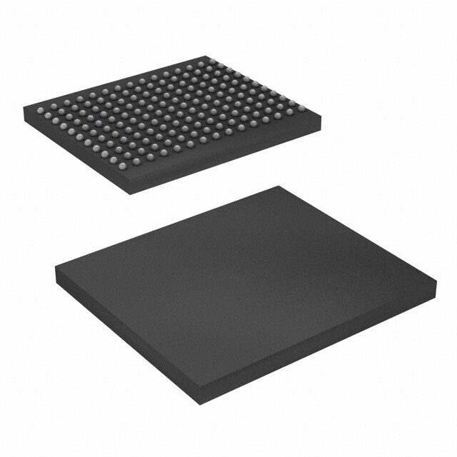
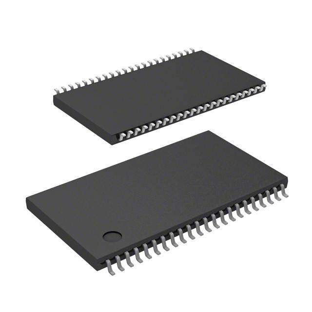
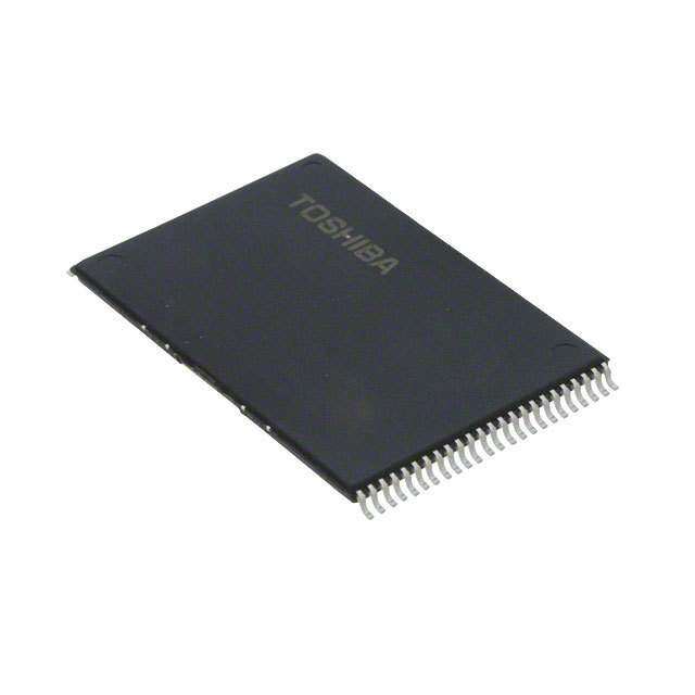
| 供应商器件封装 | 50-TSOP II |
| 其它名称 | 706-1071 |
| 包装 | 托盘 |
| 存储器类型 | SDRAM |
| 存储容量 | 16M (1M x 16) |
| 封装/外壳 | 50-TSOP(0.400",10.16mm 宽) |
| 工作温度 | 0°C ~ 70°C |
| 接口 | 并联 |
| 标准包装 | 117 |
| 格式-存储器 | RAM |
| 电压-电源 | 3 V ~ 3.6 V |
| 速度 | 143MHz |
%20Renders/50-TSOP.jpg)


- 商务部:美国ITC正式对集成电路等产品启动337调查
- 曝三星4nm工艺存在良率问题 高通将骁龙8 Gen1或转产台积电
- 太阳诱电将投资9.5亿元在常州建新厂生产MLCC 预计2023年完工
- 英特尔发布欧洲新工厂建设计划 深化IDM 2.0 战略
- 台积电先进制程称霸业界 有大客户加持明年业绩稳了
- 达到5530亿美元!SIA预计今年全球半导体销售额将创下新高
- 英特尔拟将自动驾驶子公司Mobileye上市 估值或超500亿美元
- 三星加码芯片和SET,合并消费电子和移动部门,撤换高东真等 CEO
- 三星电子宣布重大人事变动 还合并消费电子和移动部门
- 海关总署:前11个月进口集成电路产品价值2.52万亿元 增长14.8%


PDF Datasheet 数据手册内容提取
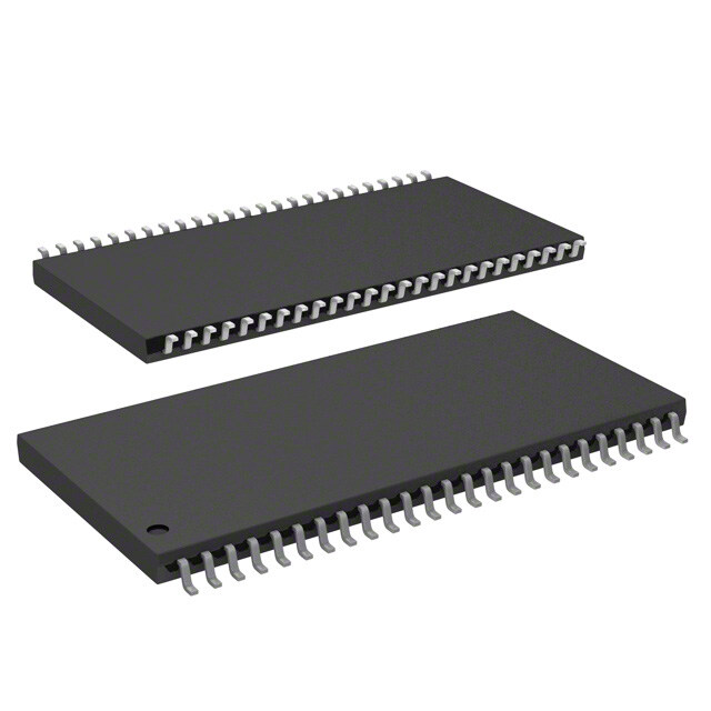
IS42S16100E IC42S16100E 512K Words x 16 Bits x 2 Banks (16-MBIT) JANUARY 2008 SYNCHRONOUS DYNAMIC RAM FEATURES DESCRIPTION • Clock frequency: 200, 166, 143 MHz ISSI’s 16Mb Synchronous DRAM IS42S16100E/ • Fully synchronous; all signals referenced to a IC42S16100E is organized as a 524,288-word x 16-bit x 2-bank for improved performance. The synchronous positive clock edge DRAMs achieve high-speed data transfer using pipeline • Two banks can be operated simultaneously and architecture. All inputs and outputs signals refer to the independently rising edge of the clock input. • Dual internal bank controlled by A11 (bank select) PIN CONFIGURATIONS • Single 3.3V power supply 50-Pin TSOP (Type II) • LVTTL interface VDD 1 50 GND • Programmable burst length DQ0 2 49 DQ15 – (1, 2, 4, 8, full page) DQ1 3 48 IDQ14 GNDQ 4 47 GNDQ • Programmable burst sequence: DQ2 5 46 DQ13 DQ3 6 45 DQ12 Sequential/Interleave VDDQ 7 44 VDDQ DQ4 8 43 DQ11 • 2048 refresh cycles every 32 ms DQ5 9 42 DQ10 GNDQ 10 41 GNDQ • Random column address every clock cycle DQ6 11 40 DQ9 • Programmable CAS latency (2, 3 clocks) DQ7 12 39 DQ8 VDDQ 13 38 VDDQ • Burst read/write and burst read/single write LDQM 14 37 NC WE 15 36 UDQM operations capability CAS 16 35 CLK RAS 17 34 CKE • Burst termination by burst stop and CS 18 33 NC precharge command A11 19 32 A9 A10 20 31 A8 • Byte controlled by LDQM and UDQM A0 21 30 A7 A1 22 29 A6 • Packages 400-mil 50-pin TSOP-II and 60-ball A2 23 28 A5 A3 24 27 A4 BGA VDD 25 26 GND • Lead-free package option • Available in Industrial Temperature PIN DESCRIPTIONS A0-A11 Address Input CAS Column Address Strobe Command A0-A10 Row Address Input WE Write Enable A11 Bank Select Address LDQM Lower Bye, Input/Output Mask A0-A7 Column Address Input UDQM Upper Bye, Input/Output Mask DQ0 to DQ15 Data DQ VDD Power CLK System Clock Input GND Ground CKE Clock Enable VDDQ Power Supply for DQ Pin CS Chip Select GNDQ Ground for DQ Pin RAS Row Address Strobe Command NC No Connection Copyright © 2006 Integrated Silicon Solution, Inc. All rights reserved. ISSI reserves the right to make changes to this specification and its products at any time without notice. ISSI assumes no liability arising out of the application or use of any information, products or services described herein. Customers are advised to obtain the latest version of this device specification before relying on any published information and before placing orders for products. Integrated Silicon Solution, Inc. — www.issi.com 1 Rev. C 01/22/08
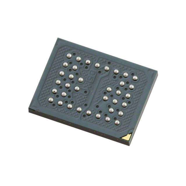
IS42S16100E, IC42S16100E PIN CONFIGURATION PACKAGE CODE: B 60 BALL FBGA (Top View) (10.1 mm x 6.4 mm Body, 0.65 mm Ball Pitch) 1 2 3 4 5 6 7 A VSS DQ15 DQ0 VDD B DQ14 VSSQ VDDQ DQ1 C DQ13 VDDQ VSSQ DQ2 D DQ12 DQ11 DQ4 DQ3 E DQ10 VSSQ VDDQ DQ5 F DQ9 VDDQ VSSQ DQ6 G DQ8 NC NC DQ7 H NC NC VDD NC J NC UDQM LDQM WE K NC CLK RAS CAS L CKE NC NC CS M A11 A9 NC NC N A8 A7 A0 A10 P A6 A5 A2 A1 R VSS A4 A3 VDD PIN DESCRIPTIONS A0-A10 Row Address Input WE Write Enable A0-A7 Column Address Input LDQM, UDQM x16 Input/Output Mask A11 Bank Select Address Vdd Power DQ0 to DQ15 Data I/O Vss Ground CLK System Clock Input Vddq Power Supply for I/O Pin CKE Clock Enable Vssq Ground for I/O Pin CS Chip Select NC No Connection RAS Row Address Strobe Command CAS Column Address Strobe Command 2 Integrated Silicon Solution, Inc. — www.issi.com Rev. C 01/22/08
IS42S16100E, IC42S16100E PIN FUNCTIONS Pin No. Symbol Type Function (In Detail) 20 to 24 A0-A10 Input Pin A0 to A10 are address inputs. A0-A10 are used as row address inputs during active 27 to 32 command input and A0-A7 as column address inputs during read or write command input. A10 is also used to determine the precharge mode during other commands. If A10 is LOW during precharge command, the bank selected by A11 is precharged, but if A10 is HIGH, both banks will be precharged. When A10 is HIGH in read or write command cycle, the precharge starts automatically after the burst access. These signals become part of the OP CODE during mode register set command input. 19 A11 Input Pin A11 is the bank selection signal. When A11 is LOW, bank 0 is selected and when high, bank 1 is selected. This signal becomes part of the OP CODE during mode register set command input. 16 CAS Input Pin CAS, in conjunction with the RAS and WE, forms the device command. See the “Command Truth Table” item for details on device commands. 34 CKE Input Pin The CKE input determines whether the CLK input is enabled within the device. When is CKE HIGH, the next rising edge of the CLK signal will be valid, and when LOW, invalid. When CKE is LOW, the device will be in either the power-down mode, the clock suspend mode, or the self refresh mode. The CKE is an asynchronous input. 35 CLK Input Pin CLK is the master clock input for this device. Except for CKE, all inputs to this device are acquired in synchronization with the rising edge of this pin. 18 CS Input Pin The CS input determines whether command input is enabled within the device. Command input is enabled when CS is LOW, and disabled with CS is HIGH. The device remains in the previous state when CS is HIGH. 2, 3, 5, 6, 8, 9, 11 DQ0 to DQ Pin DQ0 to DQ15 are DQ pins. DQ through these pins can be controlled in byte units 12, 39, 40, 42, 43, DQ15 using the LDQM and UDQM pins. 45, 46, 48, 49 14, 36 LDQM, Input Pin LDQM and UDQM control the lower and upper bytes of the DQ buffers. In read UDQM mode, LDQM and UDQM control the output buffer. When LDQM or UDQM is LOW, the corresponding buffer byte is enabled, and when HIGH, disabled. The outputs go to the HIGH impedance state when LDQM/UDQM is HIGH. This function corresponds to OE in conventional DRAMs. In write mode, LDQM and UDQM control the input buffer. When LDQM or UDQM is LOW, the corresponding buffer byte is enabled, and data can be written to the device. When LDQM or UDQM is HIGH, input data is masked and cannot be written to the device. 17 RAS Input Pin RAS, in conjunction with CAS and WE, forms the device command. See the “Command Truth Table” item for details on device commands. 15 WE Input Pin WE, in conjunction with RAS and CAS, forms the device command. See the “Command Truth Table” item for details on device commands. 7, 13, 38, 44 VddQ Power Supply Pin VddQ is the output buffer power supply. 1, 25 Vdd Power Supply Pin Vdd is the device internal power supply. 4, 10, 41, 47 GNdQ Power Supply Pin GNdQ is the output buffer ground. 26, 50 GNd Power Supply Pin GNd is the device internal ground. Integrated Silicon Solution, Inc. — www.issi.com 3 Rev. C 01/22/08
IS42S16100E, IC42S16100E FUNCTIONAL BLOCK DIAGRAM CLK CKE CS COMMAND R E RAS DECODER D MEMORY CELL ROW O CAS & C ARRAY ADDRESS E 2048 WE CLOCK D A11 GENERATOR MODE 11 BUFFER 11 W BANK 0 REGISTER O DQM R 11 DATA IN SENSE AMP I/O GATE BUFFER A1AAAA09876 CORRNEETFFRRROEELSSLHHER CORNE TSFREROLEFLSLHER 8 COLUMNADDRESS LATCH BURST COUNTER COLUMNADDRESS BUFFER 8 CSOENLUSEM 2A2NM55 6DP6 EI/OC OGADTEER 16 DATA OUT 16 DQ 0-15 A5 BUFFER COUNTER A4 16 16 R A3 E D MEMORY CELL A2 R O VDD/VDDQ E C ARRAY A1 EX ROW DE 2048 GND/GNDQ A0 PL ADDRESS W BANK 1 ROW TI BUFFER O L 11 11 R ADDRESS U M LATCH 11 S16BLK.eps 4 Integrated Silicon Solution, Inc. — www.issi.com Rev. C 01/22/08
IS42S16100E, IC42S16100E ABSOLUTE MAXIMUM RATINGS(1) Symbol Parameters Rating Unit V dd max Maximum Supply Voltage –1.0 to +4.6 V V ddq max Maximum Supply Voltage for Output Buffer –1.0 to +4.6 V V iN Input Voltage –1.0 to +4.6 V V out Output Voltage –1.0 to +4.6 V P d max Allowable Power Dissipation 1 W I cs output Shorted Current 50 mA T opr operating Temperature Com 0 to +70 °C Ind. -40 to +85 °C T stg Storage Temperature –55 to +150 °C DC RECOMMENDED OPERATING CONDITIONS(2) (At Ta = 0 to +70°C) Symbol Parameter Min. Typ. Max. Unit V dd, Vddq Supply Voltage 3.0 3.3 3.6 V Vih Input High Voltage(3) 2.0 — Vdd + 0.3 V V il Input Low Voltage(4) -0.3 — +0.8 V CAPACITANCE CHARACTERISTICS(1,2) (At Ta = 0 to +25°C, VDD = VDDQ = 3.3 ± 0.3V, f = 1 MHz) Symbol Parameter Typ. Max. Unit C iN1 Input Capacitance: A0-A11 — 4 pF C iN2 Input Capacitance: (CLK, CKE, CS, RAS, CAS, WE, LDQM, UDQM) — 4 pF CI/O Data Input/Output Capacitance: DQ0-DQ15 — 5 pF Notes: 1. Stress greater than those listed under ABSOLUTE MAXIMUM RATINGS may cause permanent damage to the device. This is a stress rating only and functional operation of the device at these or any other conditions above those indicated in the operational sections of this specification is not implied. Exposure to absolute maximum rating conditions for extended periods may affect reliability. 2. All voltages are referenced to GND. 3. Vih (max) = Vddq + 2.0V with a pulse width ≤ 3 ns. Integrated Silicon Solution, Inc. — www.issi.com 5 Rev. C 01/22/08
IS42S16100E, IC42S16100E DC ELECTRICAL CHARACTERISTICS (Recommended Operation Conditions unless otherwise noted.) Symbol Parameter Test Condition Speed Min. Max. Unit iil Input Leakage Current 0V ≤ ViN ≤ Vdd, with pins other than –5 5 µA the tested pin at 0V iol Output Leakage Current Output is disabled, 0V ≤ Vout ≤ Vdd –5 5 µA Voh Output High Voltage Level iout = –2 mA 2.4 — V Vol Output Low Voltage Level iout = +2 mA — 0.4 V icc1 Operating Current(1,2) One Bank Operation, CAS latency = 3 Com. -5 — 170 mA Burst Length=1 Com. -6 — 160 trc ≥ trc (min.) Com. -7 — 140 Iout = 0mA Ind. -6 — 170 Ind. -7 — 160 icc2p Precharge Standby Current CKE ≤ Vil (max) tck = tck (miN) Com. — — 3 mA Ind. — — 4 Icc2ps (In Power-Down Mode) tck = ∞ Com. — — 2 Ind. — — — icc3N Active Standby Current CKE ≥ Vih (miN) tck = tck (miN) — — 40 mA Icc3Ns (In Non Power-Down Mode) tck = ∞ Com. — — 30 Ind. — — 30 icc4 Operating Current tck = tck (miN) CAS latency = 3 Com. -5 — 170 mA (In Burst Mode)(1) Iout = 0mA Com. -6 — 150 Ind. -6 — 170 Com. -7 — 130 Ind. -7 — 150 CAS latency = 2 Com. -5 — 170 mA Com. -6 — 150 Ind. -6 — 170 Com. -7 — 130 Ind. -7 — 150 icc5 Auto-Refresh Current trc = trc (miN) CAS latency = 3 Com. -5 — 120 mA Com. -6 — 100 Ind. -6 — 110 Com. -7 — 70 Ind. -7 — 90 CAS latency = 2 Com. -5 — 120 mA Com. -6 — 100 Ind. -6 — 110 Com. -7 — 70 Ind. -7 — 90 icc6 Self-Refresh Current CKE ≤ 0.2V — — 2 mA Notes: 1. These are the values at the minimum cycle time. Since the currents are transient, these values decrease as the cycle time in- creases. Also note that a bypass capacitor of at least 0.01 µF should be inserted between Vdd and GND for each memory chip to suppress power supply voltage noise (voltage drops) due to these transient currents. 2. Icc1 and Icc4 depend on the output load. The maximum values for Icc1 and Icc4 are obtained with the output open state. 6 Integrated Silicon Solution, Inc. — www.issi.com Rev. C 01/22/08
IS42S16100E, IC42S16100E AC CHARACTERISTICS(1,2,3) -5 -6 -7 Symbol Parameter Min. Max. Min. Max. Min. Max. Units t ck3 Clock Cycle Time CAS Latency = 3 5 — 6 — 7 — ns t ck2 CAS Latency = 2 8 — 8 — 8 — ns t ac3 Access Time From CLK(4) CAS Latency = 3 — 5 — 5.5 — 5.5 ns t ac2 CAS Latency = 2 — 6 — 6 — 6 ns t chi CLK HIGH Level Width 2 — 2.5 — 2.5 — ns t cl CLK LOW Level Width 2 — 2.5 — 2.5 — ns t oh3 Output Data Hold Time CAS Latency = 3 2 — 2.0 — 2.0 — ns t oh2 CAS Latency = 2 2.5 — 2.5 — 2.5 — ns t lz Output LOW Impedance Time 0 — 0 — 0 — ns t hz3 Output HIGH Impedance Time(5) CAS Latency = 3 — 4 — 5.5 — 5.5 ns t hz2 CAS Latency = 2 — 6 — 6 — 6 ns t ds Input Data Setup Time 2 — 2 — 2 — ns t dh Input Data Hold Time 1 — 1 — 1 — ns t as Address Setup Time 2 — 2 — 2 — ns t ah Address Hold Time 1 — 1 — 1 — ns t cks CKE Setup Time 2 — 2 — 2 — ns t ckh CKE Hold Time 1 — 1 — 1 — ns t cka CKE to CLK Recovery Delay Time 1CLK+3 — 1CLK+3 — 1CLK+3 — ns t cs Command Setup Time (CS, RAS, CAS, WE, DQM) 2 — 2 — 2 — ns t ch Command Hold Time (CS, RAS, CAS, WE, DQM) 1 — 1 — 1 — ns t rc Command Period (REF to REF / ACT to ACT) 48 — 54 — 63 — ns t ras Command Period (ACT to PRE) 32 — 36 100,000 42 100,000 ns t rp Command Period (PRE to ACT) 16 — 18 — 20 — ns t rcd Active Command To Read / Write Command Delay Time 16 — 16 — 16 — ns t rrd Command Period (ACT [0] to ACT[1]) 11 — 12 — 14 — ns t dpl3 Input Data To Precharge CAS Latency = 3 — 2CLK 2CLK — 2CLK — ns Command Delay time t dpl2 CAS Latency = 2 — 2CLK 2CLK — 2CLK — ns t dal3 Input Data To Active / Refresh CAS Latency = 3 2CLK+trp — 2CLK+trp — 2CLK+trp — ns Command Delay time (During Auto-Precharge) t dal2 CAS Latency = 2 2CLK+trp — 2CLK+trp — 2CLK+trp — ns t t Transition Time 1 10 1 10 1 10 ns t ref Refresh Cycle Time (2048) — 32 — 32 — 32 ms Notes: 1. When power is first applied, memory operation should be started 100 µs after Vdd and Vddq reach their stipulated voltages. Also note that the power-on sequence must be executed before starting memory operation. 2. measured with tt = 1 ns. 3. The reference level is 1.4 V when measuring input signal timing. Rise and fall times are measured between Vih (min.) and Vil (max.). 4. Access time is measured at 1.4V with the load shown in the figure below. 5. The time thz (max.) is defined as the time required for the output voltage to transition by ± 200 mV from Voh (min.) or Vol (max.) when the output is in the high impedance state. Integrated Silicon Solution, Inc. — www.issi.com 7 Rev. C 01/22/08
IS42S16100E, IC42S16100E OPERATING FREQUENCY / LATENCY RELATIONSHIPS SYMBOL PARAMETER -5 -6 -7 UNITS — Clock Cycle Time 5 6 7 ns — Operating Frequency 200 166 143 MHz t cac CAS Latency 3 3 3 cycle t rcd Active Command To Read/Write Command Delay Time 3 3 3 cycle t rac RAS Latency (trcd + tcac) 6 6 6 cycle t rc Command Period (REF to REF / ACT to ACT) 9 9 9 cycle t ras Command Period (ACT to PRE) 6 6 6 cycle t rp Command Period (PRE to ACT) 3 3 3 cycle t rrd Command Period (ACT[0] to ACT [1]) 2 2 2 cycle t ccd Column Command Delay Time 1 1 1 cycle (READ, READA, WRIT, WRITA) t dpl Input Data To Precharge Command Delay Time 2 2 2 cycle t dal Input Data To Active/Refresh Command Delay Time 5 5 5 cycle (During Auto-Precharge) t rbd Burst Stop Command To Output in HIGH-Z Delay Time 3 3 3 cycle (Read) t wbd Burst Stop Command To Input in Invalid Delay Time 0 0 0 cycle (Write) t rql Precharge Command To Output in HIGH-Z Delay Time 3 3 3 cycle (Read) t wdl Precharge Command To Input in Invalid Delay Time 0 0 0 cycle (Write) t pql Last Output To Auto-Precharge Start Time (Read) -2 –2 –1 cycle t qmd DQM To Output Delay Time (Read) 2 2 2 cycle t dmd DQM To Input Delay Time (Write) 0 0 0 cycle t mcd Mode Register Set To Command Delay Time 2 2 2 cycle AC TEST CONDITIONS (Input/Output Reference Level: 1.4V) Input Output Load tCK tCHI tCL 2.8V 50 Ω CLK 1.4V 0.0V I/O +1.4V tCS tCH 2.8V INPUT1.4V 50 pF 0.0V tOH tAC OUTPUT 1.4V 1.4V 8 Integrated Silicon Solution, Inc. — www.issi.com Rev. C 01/22/08
IS42S16100E, IC42S16100E COMMANDS Active Command Read Command CLK CLK CKE HIGH CKE HIGH CS CS RAS RAS CAS CAS WE WE A0-A9 ROW A0-A9 COLUMN(1) AUTO PRECHARGE A10 ROW A10 NO PRECHARGE BANK 1 BANK 1 A11 A11 BANK 0 BANK 0 Write Command Precharge Command CLK CLK CKE HIGH CKE HIGH CS CS RAS RAS CAS CAS WE WE A0-A9 COLUMN(1) A0-A9 AUTO PRECHARGE BANK 0 AND BANK 1 A10 A10 NO PRECHARGE BANK 0 OR BANK 1 BANK 1 BANK 1 A11 A11 BANK 0 BANK 0 Don't Care Notes: 1. A8-A9 = Don’t Care. Integrated Silicon Solution, Inc. — www.issi.com 9 Rev. C 01/22/08
IS42S16100E, IC42S16100E COMMANDS (cont.) No-Operation Command Device Deselect Command CLK CLK CKE HIGH CKE HIGH CS CS RAS RAS CAS CAS WE WE A0-A9 A0-A9 A10 A10 A11 A11 Mode Register Set Command Auto-Refresh Command CLK CLK CKE HIGH CKE HIGH CS CS RAS RAS CAS CAS WE WE A0-A9 OP-CODE A0-A9 A10 OP-CODE A10 A11 OP-CODE A11 Don't Care 10 Integrated Silicon Solution, Inc. — www.issi.com Rev. C 01/22/08
IS42S16100E, IC42S16100E COMMANDS (cont.) Self-Refresh Command Power Down Command CLK CLK CKE CKE ALL BANKS IDLE CS CS NOP RAS RAS NOP CAS CAS NOP WE WE NOP A0-A9 A0-A9 A10 A10 A11 A11 Clock Suspend Command Burst Stop Command CLK CLK CKE BANK(S) ACTIVE CKE HIGH CS NOP CS RAS NOP RAS CAS NOP CAS WE NOP WE A0-A9 A0-A9 A10 A10 A11 A11 Integrated Silicon Solution, Inc. — www.issi.com 11 Rev. C 01/22/08
IS42S16100E, IC42S16100E Mode Register Set Command (CS, RAS, CAS, WE = LOW) When the A10 pin is HIGH, this command functions as a read with auto-precharge command. After the burst read The IS42S16100E/IC42S16100E product incorporates completes, the bank selected by pin A11 is precharged. a register that defines the device operating mode. This When the A10 pin is LOW, the bank selected by the A11 command functions as a data input pin that loads this pin remains in the activated state after the burst read register from the pins A0 to A11. When power is first completes. applied, the stipulated power-on sequence should be executed and then the IS42S16100E/IC42S16100E should be initialized by executing a mode register set Write Command command. (CS, CAS, WE = LOW, RAS = HIGH) Note that the mode register set command can be executed only when both banks are in the idle state (i.e. When burst write mode has been selected with the mode deactivated). register set command, this command selects the bank specified by the A11 pin and starts a burst write operation Another command cannot be executed after a mode at the start address specified by pins A0 to A9. This first register set command until after the passage of the period data must be input to the DQ pins in the cycle in which tmcd, which is the period required for mode register set this command. command execution. The selected bank must be activated before executing this command. Active Command When A10 pin is HIGH, this command functions as a (CS, RAS = LOW, CAS, WE= HIGH) write with auto-precharge command. After the burst write completes, the bank selected by pin A11 is precharged. The IS42S16100E/IC42S16100E includes two banks of When the A10 pin is low, the bank selected by the A11 2048 rows each. This command selects one of the two pin remains in the activated state after the burst write banks according to the A11 pin and activates the row completes. selected by the pins A0 to A10. After the input of the last burst write data, the application This command corresponds to the fall of the RAS signal must wait for the write recovery period (tdpl, tdal) to elapse from HIGH to LOW in conventional DRAMs. according to CAS latency. Precharge Command Auto-Refresh Command (CS, RAS, WE = LOW, CAS = HIGH) (CS, RAS, CAS = LOW, WE, CKE = HIGH) This command starts precharging the bank selected by This command executes the auto-refresh operation. The pins A10 and A11. When A10 is HIGH, both banks are row address and bank to be refreshed are automatically precharged at the same time. When A10 is LOW, the generated during this operation. bank selected by A11 is precharged. After executing this command, the next command for the selected bank(s) Both banks must be placed in the idle state before executing is executed after passage of the period trp, which is the this command. period required for bank precharging. The stipulated period (trc) is required for a single refresh This command corresponds to the RAS signal from LOW operation, and no other commands can be executed to HIGH in conventional DRAMs during this period. The device goes to the idle state after the internal refresh operation completes. Read Command This command must be executed at least 4096 times (CS, CAS = LOW, RAS, WE = HIGH) every 64 ms. This command selects the bank specified by the A11 pin This command corresponds to CBR auto-refresh in and starts a burst read operation at the start address conventional DRAMs. specified by pins A0 to A9. Data is output following CAS latency. The selected bank must be activated before executing this command. 12 Integrated Silicon Solution, Inc. — www.issi.com Rev. C 01/22/08
IS42S16100E, IC42S16100E Self-Refresh Command Power-Down Command (CS, RAS, CAS, CKE = LOW, WE = HIGH) (CKE = LOW) This command executes the self-refresh operation. The When both banks are in the idle (inactive) state, or when row address to be refreshed, the bank, and the refresh at least one of the banks is not in the idle (inactive) state, interval are generated automatically internally during this this command can be used to suppress device power operation. The self-refresh operation is started by dropping dissipation by reducing device internal operations to the CKE pin from HIGH to LOW. The self-refresh operation the absolute minimum. Power-down mode is started by continues as long as the CKE pin remains LOW and there dropping the CKE pin from HIGH to LOW. Power-down is no need for external control of any other pins. The mode continues as long as the CKE pin is held low. All self-refresh operation is terminated by raising the CKE pins other than the CKE pin are invalid and none of the pin from LOW to HIGH. The next command cannot be other commands can be executed in this mode. The executed until the device internal recovery period (trc) power-down operation is terminated by raising the CKE has elapsed. After the self-refresh, since it is impossible pin from LOW to HIGH. The next command cannot be to determine the address of the last row to be refreshed, executed until the recovery period (tcka) has elapsed. an auto-refresh should immediately be performed for all Since this command differs from the self-refresh command addresses (4096 cycles). described above in that the refresh operation is not Both banks must be placed in the idle state before executing performed automatically internally, the refresh operation this command. must be performed within the refresh period (tref). Thus the maximum time that power-down mode can be held is just under the refresh cycle time. Burst Stop Command (CS, WE, = LOW, RAS, CAS = HIGH) Clock Suspend The command forcibly terminates burst read and write (CKE = LOW) operations. When this command is executed during a burst read operation, data output stops after the CAS This command can be used to stop the device internal clock latency period has elapsed. temporarily during a read or write cycle. Clock suspend mode is started by dropping the CKE pin from HIGH to LOW. Clock suspend mode continues as long as the No Operation CKE pin is held LOW. All input pins other than the CKE pin are invalid and none of the other commands can be (CS, = LOW, RAS, CAS, WE = HIGH) executed in this mode. Also note that the device internal This command has no effect on the device. state is maintained. Clock suspend mode is terminated by raising the CKE pin from LOW to HIGH, at which point device operation restarts. The next command cannot be Device Deselect Command executed until the recovery period (tcka) has elapsed. (CS = HIGH) Since this command differs from the self-refresh command described above in that the refresh operation is not This command does not select the device for an object of performed automatically internally, the refresh operation operation. In other words, it performs no operation with respect to the device. must be performed within the refresh period (tref). Thus the maximum time that clock suspend mode can be held is just under the refresh cycle time. Integrated Silicon Solution, Inc. — www.issi.com 13 Rev. C 01/22/08
IS42S16100E, IC42S16100E COMMAND TRUTH TABLE(1,2) CKE Symbol Command n-1 n CS RAS CAS WE DQM A11 A10 A9-A0 I/On MRS Mode Register Set(3,4) H X L L L L X OP CODE X REF Auto-Refresh(5) H H L L L H X X X X HIGH-Z SREF Self-Refresh(5,6) H L L L L H X X X X HIGH-Z PRE Precharge Selected Bank H X L L H L X BS L X X PALL Precharge Both Banks H X L L H L X X H X X ACT Bank Activate(7) H X L L H H X BS Row Row X WRIT Write H X L H L L X BS L Column(18) X WRITA Write With Auto-Precharge(8) H X L H L L X BS H Column(18) X READ Read(8) H X L H L H X BS L Column(18) X READA Read With Auto-Precharge(8) H X L H L H X BS H Column(18) X BST Burst Stop(9) H X L H H L X X X X X NOP No Operation H X L H H H X X X X X DESL Device Deselect H X H X X X X X X X X SBY Clock Suspend / Standby Mode L X X X X X X X X X X ENB Data Write / Output Enable H X X X X X L X X X Active MASK Data Mask / Output Disable H X X X X X H X X X HIGH-Z DQM TRUTH TABLE(1,2) CKE DQM Symbol Command n-1 n UPPER LOWER ENB Data Write / Output Enable H X L L MASK Data Mask / Output Disable H X H H ENBU Upper Byte Data Write / Output Enable H X L X ENBL Lower Byte Data Write / Output Enable H X X L MASKU Upper Byte Data Mask / Output Disable H X H X MASKL Lower Byte Data Mask / Output Disable H X X H CKE TRUTH TABLE(1,2) CKE Symbol Command Current State n-1 n CS RAS CAS WE A11 A10 A9-A0 SPND Start Clock Suspend Mode Active H L X X X X X X X — Clock Suspend Other States L L X X X X X X X — Terminate Clock Suspend Mode Clock Suspend L H X X X X X X X REF Auto-Refresh Idle H H L L L H X X X SELF Start Self-Refresh Mode Idle H L L L L H X X X SELFX Terminate Self-Refresh Mode Self-Refresh L H L H H H X X X L H H X X X X X X PDWN Start Power-Down Mode Idle H L L H H H X X X H L H X X X X X X — Terminate Power-Down Mode Power-Down L H X X X X X X X 14 Integrated Silicon Solution, Inc. — www.issi.com Rev. C 01/22/08
IS42S16100E, IC42S16100E OPERATION COMMAND TABLE(1,2) Current State Command Operation CS RAS CAS WE A11 A10 A9-A0 Idle DESL No Operation or Power-Down(12) H X X X X X X NOP No Operation or Power-Down(12) L H H H X X X BST No Operation or Power-Down L H H L X X X READ / READA Illegal L H L H V V V(18) WRIT/WRITA Illegal L H L L V V V(18) ACT Row Active L L H H V V V(18) PRE/PALL No Operation L L H L V V X REF/SELF Auto-Refresh or Self-Refresh(13) L L L H X X X MRS Mode Register Set L L L L OP CODE Row Active DESL No Operation H X X X X X X NOP No Operation L H H H X X X BST No Operation L H H L X X X READ/READA Read Start(17) L H L H V V V(18) WRIT/WRITA Write Start(17) L H L L V V V(18) ACT Illegal(10) L L H H V V V(18) PRE/PALL Precharge(15) L L H L V V X REF/SELF Illegal L L L H X X X MRS Illegal L L L L OP CODE Read DESL Burst Read Continues, Row Active When Done H X X X X X X NOP Burst Read Continues, Row Active When Done L H H H X X X BST Burst Interrupted, Row Active After Interrupt L H H L X X X READ/READA Burst Interrupted, Read Restart After Interrupt(16) L H L H V V V(18) WRIT/WRITA Burst Interrupted Write Start After Interrupt(11,16) L H L L V V V(18) ACT Illegal(10) L L H H V V V(18) PRE/PALL Burst Read Interrupted, Precharge After Interrupt L L H L V V X REF/SELF Illegal L L L H X X X MRS Illegal L L L L OP CODE Write DESL Burst Write Continues, Write Recovery When Done H X X X X X X NOP Burst Write Continues, Write Recovery When Done L H H H X X X BST Burst Write Interrupted, Row Active After Interrupt L H H L X X X READ/READA Burst Write Interrupted, Read Start After Interrupt(11,16) L H L H V V V(18) WRIT/WRITA Burst Write Interrupted, Write Restart After Interrupt(16) L H L L V V V(18) ACT Illegal(10) L L H H V V V(18) PRE/PALL Burst Write Interrupted, Precharge After Interrupt L L H L V V X REF/SELF Illegal L L L H X X X MRS Illegal L L L L OP CODE Read With DESL Burst Read Continues, Precharge When Done H X X X X X X Auto- NOP Burst Read Continues, Precharge When Done L H H H X X X Precharge BST Illegal L H H L X X X READ/READA Illegal L H L H V V V(18) WRIT/WRITA Illegal L H L L V V V(18) ACT Illegal(10) L L H H V V V(18) PRE/PALL Illegal(10) L L H L V V X REF/SELF Illegal L L L H X X X MRS Illegal L L L L OP CODE Integrated Silicon Solution, Inc. — www.issi.com 15 Rev. C 01/22/08
IS42S16100E, IC42S16100E OPERATION COMMAND TABLE(1,2) Current State Command Operation CS RAS CAS WE A11 A10 A9-A0 Write With DESL Burst Write Continues, Write Recovery And Precharge H X X X X X X Auto-Precharge When Done NOP Burst Write Continues, Write Recovery And Precharge L H H H X X X BST Illegal L H H L X X X READ/READA Illegal L H L H V V V(18) WRIT/WRITA Illegal L H L L V V V(18) ACT Illegal(10) L L H H V V V(18) PRE/PALL Illegal(10) L L H L V V X REF/SELF Illegal L L L H X X X MRS Illegal L L L L OPCODE Row Precharge DESL No Operation, Idle State After trp Has Elapsed H X X X X X X NOP No Operation, Idle State After trp Has Elapsed L H H H X X X BST No Operation, Idle State After trp Has Elapsed L H H L X X X READ/READA Illegal(10) L H L H V V V(18) WRIT/WRITA Illegal(10) L H L L V V V(18) ACT Illegal(10) L L H H V V V(18) PRE/PALL No Operation, Idle State After trp Has Elapsed(10) L L H L V V X REF/SELF Illegal L L L H X X X MRS Illegal L L L L OP CODE Immediately DESL No Operation, Row Active After trcd Has Elapsed H X X X X X X Following NOP No Operation, Row Active After trcd Has Elapsed L H H H X X X Row Active BST No Operation, Row Active After trcd Has Elapsed L H H L X X X READ/READA Illegal(10) L H L H V V V(18) WRIT/WRITA Illegal(10) L H L L V V V(18) ACT Illegal(10,14) L L H H V V V(18) PRE/PALL Illegal(10) L L H L V V X REF/SELF Illegal L L L H X X X MRS Illegal L L L L OP CODE Write DESL No Operation, Row Active After tdpl Has Elapsed H X X X X X X Recovery NOP No Operation, Row Active After tdpl Has Elapsed L H H H X X X BST No Operation, Row Active After tdpl Has Elapsed L H H L X X X READ/READA Read Start L H L H V V V(18) WRIT/WRITA Write Restart L H L L V V V(18) ACT Illegal(10) L L H H V V V(18) PRE/PALL Illegal(10) L L H L V V X REF/SELF Illegal L L L H X X X MRS Illegal L L L L OP CODE 16 Integrated Silicon Solution, Inc. — www.issi.com Rev. C 01/22/08
IS42S16100E, IC42S16100E OPERATION COMMAND TABLE(1,2) Current State Command Operation CS RAS CAS WE A11 A10 A9-A0 Write Recovery DESL No Operation, Idle State After tdal Has Elapsed H X X X X X X With Auto- NOP No Operation, Idle State After tdal Has Elapsed L H H H X X X Precharge BST No Operation, Idle State After tdal Has Elapsed L H H L X X X READ/READA Illegal(10) L H L H V V V(18) WRIT/WRITA Illegal(10) L H L L V V V(18) ACT Illegal(10) L L H H V V V(18) PRE/PALL Illegal(10) L L H L V V X REF/SELF Illegal L L L H X X X MRS Illegal L L L L OP CODE Refresh DESL No Operation, Idle State After trp Has Elapsed H X X X X X X NOP No Operation, Idle State After trp Has Elapsed L H H H X X X BST No Operation, Idle State After trp Has Elapsed L H H L X X X READ/READA Illegal L H L H V V V(18) WRIT/WRITA Illegal L H L L V V V(18) ACT Illegal L L H H V V V(18) PRE/PALL Illegal L L H L V V X REF/SELF Illegal L L L H X X X MRS Illegal L L L L OP CODE Mode Register DESL No Operation, Idle State After tmcd Has Elapsed H X X X X X X Set NOP No Operation, Idle State After tmcd Has Elapsed L H H H X X X BST No Operation, Idle State After tmcd Has Elapsed L H H L X X X READ/READA Illegal L H L H V V V(18) WRIT/WRITA Illegal L H L L V V V(18) ACT Illegal L L H H V V V(18) PRE/PALL Illegal L L H L V V X REF/SELF Illegal L L L H X X X MRS Illegal L L L L OP CODE Notes: 1. H: HIGH level input, L: LOW level input, X: HIGH or LOW level input, V: Valid data input 2. All input signals are latched on the rising edge of the CLK signal. 3. Both banks must be placed in the inactive (idle) state in advance. 4. The state of the A0 to A11 pins is loaded into the mode register as an OP code. 5. The row address is generated automatically internally at this time. The DQ pin and the address pin data is ignored. 6. During a self-refresh operation, all pin data (states) other than CKE is ignored. 7. The selected bank must be placed in the inactive (idle) state in advance. 8. The selected bank must be placed in the active state in advance. 9. This command is valid only when the burst length set to full page. 10. This is possible depending on the state of the bank selected by the A11 pin. 11. Time to switch internal busses is required. 12. The IS42S16100E/IC42S16100E can be switched to power-down mode by dropping the CKE pin LOW when both banks in the idle state. Input pins other than CKE are ignored at this time. 13. The IS42S16100E/IC42S16100E can be switched to self-refresh mode by dropping the CKE pin LOW when both banks in the idle state. Input pins other than CKE are ignored at this time. 14. Possible if trrd is satisfied. 15. Illegal if tras is not satisfied. 16. The conditions for burst interruption must be observed. Also note that the IS42S16100E/IC42S16100E will enter the pre charged state immediately after the burst operation completes if auto-precharge is selected. 17. Command input becomes possible after the period trcd has elapsed. Also note that the IS42S16100E/IC42S16100E will enter the precharged state immediately after the burst operation completes if auto-precharge is selected. 18. A8,A9 = don’t care. Integrated Silicon Solution, Inc. — www.issi.com 17 Rev. C 01/22/08
IS42S16100E, IC42S16100E CKE RELATED COMMAND TRUTH TABLE(1) CKE Current State Operation n-1 n CS RAS CAS WE A11 A10 A9-A0 Self-Refresh Undefined H X X X X X X X X Self-Refresh Recovery(2) L H H X X X X X X Self-Refresh Recovery(2) L H L H H X X X X Illegal(2) L H L H L X X X X Illegal(2) L H L L X X X X X Self-Refresh L L X X X X X X X Self-Refresh Recovery Idle State After trc Has Elapsed H H H X X X X X X Idle State After trc Has Elapsed H H L H H X X X X Illegal H H L H L X X X X Illegal H H L L X X X X X Power-Down on the Next Cycle H L H X X X X X X Power-Down on the Next Cycle H L L H H X X X X Illegal H L L H L X X X X Illegal H L L L X X X X X Clock Suspend Termination on the Next Cycle (2) L H X X X X X X X Clock Suspend L L X X X X X X X Power-Down Undefined H X X X X X X X X Power-Down Mode Termination, Idle After L H X X X X X X X That Termination(2) Power-Down Mode L L X X X X X X X Both Banks Idle No Operation H H H X X X X X X See the Operation Command Table H H L H X X X X X Bank Active Or Precharge H H L L H X X X X Auto-Refresh H H L L L H X X X Mode Register Set H H L L L L OP CODE See the Operation Command Table H L H X X X X X X See the Operation Command Table H L L H X X X X X See the Operation Command Table H L L L H X X X X Self-Refresh(3) H L L L L H X X X See the Operation Command Table H L L L L L OP CODE Power-Down Mode(3) L X X X X X X X X Other States See the Operation Command Table H H X X X X X X X Clock Suspend on the Next Cycle(4) H L X X X X X X X Clock Suspend Termination on the Next Cycle L H X X X X X X X Clock Suspend Termination on the Next Cycle L L X X X X X X X Notes: 1. H: HIGH level input, L: LOW level input, X: HIGH or LOW level input 2. The CLK pin and the other input are reactivated asynchronously by the transition of the CKE level from LOW to HIGH. The minimum setup time (tcka) required before all commands other than mode termination must be satisfied. 3. Both banks must be set to the inactive (idle) state in advance to switch to power-down mode or self-refresh mode. 4. The input must be command defined in the operation command table. 18 Integrated Silicon Solution, Inc. — www.issi.com Rev. C 01/22/08
IS42S16100E, IC42S16100E TWO BANKS OPERATION COMMAND TRUTH TABLE(1,2) Previous State Next State Operation CS RAS CAS WE A11 A10 A9-A0 BANK 0 BANK 1 BANK 0 BANK 1 DESL H X X X X X X Any Any Any Any NOP L H H H X X X Any Any Any Any BST L H H L X X X R/W/A I/A A I/A I I/A I I/A I/A R/W/A I/A A I/A I I/A I READ/READA L H L H H H CA(3) I/A R/W/A I/A RP H H CA(3) R/W A A RP H L CA(3) I/A R/W/A I/A R H L CA(3) R/W A A R L H CA(3) R/W/A I/A RP I/A L H CA(3) A R/W RP A L L CA(3) R/W/A I/A R I/A L L CA(3) A R/W R A WRIT/WRITA L H L L H H CA(3) I/A R/W/A I/A WP H H CA(3) R/W A A WP H L CA(3) I/A R/W/A I/A W H L CA(3) R/W A A W L H CA(3) R/W/A I/A WP I/A L H CA(3) A R/W WP A L L CA(3) R/W/A I/A W I/A L L CA(3) A R/W W A ACT L L H H H RA RA Any I Any A L RA RA I Any A Any PRE/PALL L L H L X H X R/W/A/I I/A I I X H X I/A R/W/A/I I I H L X I/A R/W/A/I I/A I H L X R/W/A/I I/A R/W/A/I I L L X R/W/A/I I/A I I/A L L X I/A R/W/A/I I R/W/A/I REF L L L H X X X I I I I MRS L L L L OPCODE I I I I Notes: 1. H: HIGH level input, L: LOW level input, X: HIGH or LOW level input, RA: Row Address, CA: Column Address 2. The device state symbols are interpreted as follows: I Idle (inactive state) A Row Active State R Read W Write RP Read With Auto-Precharge WP Write With Auto-Precharge Any Any State 3. CA: A8,A9 = don’t care. Integrated Silicon Solution, Inc. — www.issi.com 19 Rev. C 01/22/08
IS42S16100E, IC42S16100E SIMPLIFIED STATE TRANSITION DIAGRAM (One Bank Operation) SELF REFRESH SREF entry SREF exit MODE MRS REF AUTO REGISTER IDLE REFRESH SET CKE_ CKE IDLE ACT POWER DOWN ACTIVE POWER DOWN CKE_ CKE BANK BST BST ACTIVE WRIT READ WRIT READ WRITA READA READ WRITE READ CKE_ CKE_ WRIT CLOCK CKE READA CKE CLOCK SUSPEND WRITA SUSPEND CKE_ WRITA READA CKE_ CKE CKE WRITE WITH READ WITH AUTO AUTO PRECHARGE PRECHARGE PRE PRE PRE PRE PRE- POWER APPLIED POWER ON CHARGE Automatic transition following the completion of command execution. Transition due to command input. 20 Integrated Silicon Solution, Inc. — www.issi.com Rev. C 01/22/08
IS42S16100E, IC42S16100E Device Initialization At Power-On Burst Length (Power-On Sequence) When writing or reading, data can be input or output data continuously. In these operations, an address is input only As is the case with conventional DRAMs, the IS42S16100E/ once and that address is taken as the starting address IC42S16100E product must be initialized by executing a internally by the device. The device then automatically stipulated power-on sequence after power is applied. generates the following address. The burst length field in After power is applied and Vdd and VddQ reach their the mode register stipulates the number of data items input stipulated voltages, set and hold the CKE and DQM pins or output in sequence. In the IS42S16100E/IC42S16100E HIGH for 100 µs. Then, execute the precharge command product, a burst length of 1, 2, 4, 8, or full page can be to precharge both bank. Next, execute the auto-refresh specified. See the table on the next page for details on command twice or more and define the device operation setting the mode register. mode by executing a mode register set command. The mode register set command can be also set before auto-refresh command. Burst Type The burst data order during a read or write operation is stipulated by the burst type, which can be set by the mode Mode Register Settings register set command. The IS42S16100E/IC42S16100E The mode register set command sets the mode register. product supports sequential mode and interleaved mode When this command is executed, pins A0 to A9, A10, and burst type settings. See the table on the next page for A11 function as data input pins for setting the register, and details on setting the mode register. See the “Burst Length this data becomes the device internal OP code. This OP and Column Address Sequence” item for details on DQ code has four fields as listed in the table below. data orders in these modes. Input Pin Field Write Mode A11, A10, A9, A8, A7 Mode Options Burst write or single write mode is selected by the OP code A6, A5, A4 CAS Latency (A11, A10, A9) of the mode register. A3 Burst Type A burst write operation is enabled by setting the OP code A2, A1, A0 Burst Length (A11, A10, A9) to (0,0,0). A burst write starts on the same cycle as a write command set. The write start address is Note that the mode register set command can be executed specified by the column address and bank select address only when both banks are in the idle (inactive) state. Wait at the write command set cycle. at least two cycles after executing a mode register set A single write operation is enabled by setting OP code (A11, command before executing the next command. A10, A9) to (0, 0,1). In a single write operation, data is only written to the column address and bank select address specified by the write command set cycle without regard CAS Latency to the bust length setting. During a read operation, the between the execution of the read command and data output is stipulated as the CAS latency. This period can be set using the mode register set command. The optimal CAS latency is determined by the clock frequency and device speed grade. See the “Operating Frequency / Latency Relationships” item for details on the relationship between the clock frequency and the CAS latency. See the table on the next page for details on setting the mode register. Integrated Silicon Solution, Inc. — www.issi.com 21 Rev. C 01/22/08
IS42S16100E, IC42S16100E MODE REGISTER Address Bus (Ax) A11 A10 A9 A8 A7 A6 A5 A4 A3 A2 A1 A0 Mode Register (Mx) WRITE MODE LT MODE BT BL M2 M1 M0 Sequential Interleaved Burst Length 0 0 0 1 1 0 0 1 2 2 0 1 0 4 4 0 1 1 8 8 1 0 0 Reserved Reserved 1 0 1 Reserved Reserved 1 1 0 Reserved Reserved 1 1 1 Full Page Reserved M3 Type Burst Type 0 Sequential 1 Interleaved M6 M5 M4 CAS Latency Latency Mode 0 0 0 Reserved 0 0 1 Reserved 0 1 0 2 0 1 1 3 1 0 0 Reserved 1 0 1 Reserved 1 1 0 Reserved 1 1 1 Reserved M11 M10 M9 M8 M7 Write Mode 0 0 1 0 0 Burst Read & Single Write 0 0 0 0 0 Burst Read & Burst Write Note: Other values for these bits are reserved. 22 Integrated Silicon Solution, Inc. — www.issi.com Rev. C 01/22/08
IS42S16100E, IC42S16100E BURST LENGTH AND COLUMN ADDRESS SEQUENCE Column Address Address Sequence Burst Length A2 A1 A0 Sequential Interleaved 2 X X 0 0-1 0-1 X X 1 1-0 1-0 4 X 0 0 0-1-2-3 0-1-2-3 X 0 1 1-2-3-0 1-0-3-2 X 1 0 2-3-0-1 2-3-0-1 X 1 1 3-0-1-2 3-2-1-0 8 0 0 0 0-1-2-3-4-5-6-7 0-1-2-3-4-5-6-7 0 0 1 1-2-3-4-5-6-7-0 1-0-3-2-5-4-7-6 0 1 0 2-3-4-5-6-7-0-1 2-3-0-1-6-7-4-5 0 1 1 3-4-5-6-7-0-1-2 3-2-1-0-7-6-5-4 1 0 0 4-5-6-7-0-1-2-3 4-5-6-7-0-1-2-3 1 0 1 5-6-7-0-1-2-3-4 5-4-7-6-1-0-3-2 1 1 0 6-7-0-1-2-3-4-5 6-7-4-5-2-3-0-1 1 1 1 7-0-1-2-3-4-5-6 7-6-5-4-3-2-1-0 Full Page n n n Cn, Cn+1, Cn+2 None (256) Cn+3, Cn+4..... ...Cn-1(Cn+255), Cn(Cn+256)..... Notes: 1. The burst length in full page mode is 256. Integrated Silicon Solution, Inc. — www.issi.com 23 Rev. C 01/22/08
IS42S16100E, IC42S16100E BANK SELECT AND PRECHARGE ADDRESS ALLOCATION Row X0 — Row Address X1 — Row Address X2 — Row Address X3 — Row Address X4 — Row Address X5 — Row Address X6 — Row Address X7 — Row Address X8 — Row Address X9 — Row Address X10 0 Precharge of the Selected Bank (Precharge Command) Row Address 1 Precharge of Both Banks (Precharge Command) (Active Command) X11 0 Bank 0 Selected (Precharge and Active Command) 1 Bank 1 Selected (Precharge and Active Command) Column Y0 — Column Address Y1 — Column Address Y2 — Column Address Y3 — Column Address Y4 — Column Address Y5 — Column Address Y6 — Column Address Y7 — Column Address Y8 — Don’t Care Y9 — Don’t Care Y10 0 Auto-Precharge - Disabled 1 Auto-Precharge - Enables Y11 0 Bank 0 Selected (Read and Write Commands) 1 Bank 1 Selected (Read and Write Commands) 24 Integrated Silicon Solution, Inc. — www.issi.com Rev. C 01/22/08
IS42S16100E, IC42S16100E Burst Read The read cycle is started by executing the read command. is a full page is an exception. In this case the output buffers The address provided during read command execution is must be set to the high impedance state by executing a used as the starting address. First, the data corresponding to burst stop command. this address is output in synchronization with the clock signal Note that upper byte and lower byte output data can after the CAS latency period. Next, data corresponding to be masked independently under control of the signals an address generated automatically by the device is output in synchronization with the clock signal. applied to the U/LDQM pins. The delay period (tqmd) is fixed at two, regardless of the CAS latency setting, when The output buffers go to the LOW impedance state CAS this function is used. latency minus one cycle after the read command, and go to The selected bank must be set to the active state before the HIGH impedance state automatically after the last data executing this command. is output. However, the case where the burst length CLK COMMAND READ A0 tQMD=2 UDQM LDQM DQ8-DQ15 DOUT A0 DOUT A2 DOUT A3 HI-Z HI-Z DQ0-DQ 7 DOUT A0 DOUT A1 HI-Z READ (CA=A, BANK 0) DATA MASK (LOWER BYTE) CAS latency = 3, burst length = 4 DATA MASK (UPPER BYTE) Burst Write The write cycle is started by executing the command. a burst stop command. The latency for DQ pin data input The address provided during write command execution is zero, regardless of the CAS latency setting. However, a is used as the starting address, and at the same time, wait period (write recovery: tdpl) after the last data input is data for this address is input in synchronization with the required for the device to complete the write operation. clock signal. Note that the upper byte and lower byte input data can Next, data is input in other in synchronization with the be masked independently under control of the signals clock signal. During this operation, data is written to applied to the U/LDQM pins. The delay period (tdmd) is address generated automatically by the device. This cycle fixed at zero, regardless of the CAS latency setting, when terminates automatically after a number of clock cycles this function is used. determined by the stipulated burst length. However, the The selected bank must be set to the active state before case where the burst length is a full page is an exception. executing this command. In this case the write cycle must be terminated by executing CLK COMMAND WRITE DQ DIN 0 DIN 1 DIN 2 DIN 3 BURST LENGTH CAS latency = 2,3, burst length = 4 Integrated Silicon Solution, Inc. — www.issi.com 25 Rev. C 01/22/08
IS42S16100E, IC42S16100E Read With Auto-Precharge The read with auto-precharge command first executes a three, the precharge operation starts on two clock cycles burst read operation and then puts the selected bank in before the last burst data is output (tpql = –2). Therefore, the precharged state automatically. After the precharge the selected bank can be made active after a delay of trp completes, the bank goes to the idle state. Thus this from the start position of this precharge operation. command performs a read command and a precharge The selected bank must be set to the active state before command in a single operation. executing this command. During this operation, the delay period (tpql) between the The auto-precharge function is invalid if the burst length last burst data output and the start of the precharge opera- tion differs depending on the CAS latency setting. is set to full page. When the CAS latency setting is two, the precharge opera- CAS Latency 3 2 tion starts on one clock cycle before the last burst data is output (tpql = –1). When the CAS latency setting is t pql –2 –1 CLK COMMAND READA 0 ACT 0 tPQL DQ DOUT 0 DOUT 1 DOUT 2 DOUT 3 tRP READ WITH AUTO-PRECHARGE PRECHARGE START (BANK 0) CAS latency = 2, burstlength = 4 CLK COMMAND READA 0 ACT 0 tPQL DQ DOUT 0 DOUT 1 DOUT 2 DOUT 3 tRP READ WITH AUTO-PRECHARGE PRECHARGE START (BANK 0) CAS latency = 3, burstlength = 4 26 Integrated Silicon Solution, Inc. — www.issi.com Rev. C 01/22/08
IS42S16100E, IC42S16100E Write With Auto-Precharge The write with auto-precharge command first executes a Therefore, the selected bank can be made active after a burst write operation and then puts the selected bank in delay of tdal. the precharged state automatically. After the precharge The selected bank must be set to the active state before completes the bank goes to the idle state. Thus this executing this command. command performs a write command and a precharge command in a single operation. The auto-precharge function is invalid if the burst length is set to full page. During this operation, the delay period (tdal) between the last burst data input and the completion of the precharge CAS Latency 3 2 operation differs depending on the CAS latency setting. tdal 2CLK 2CLK The delay (tdal) is trp plus one CLK period. That is, the +trp +trp precharge operation starts one clock period after the last burst data input. CLK COMMAND WRITE A0 ACT 0 PRECHARGE START DQ DIN 0 DIN 1 DIN 2 DIN 3 tRP WRITE WITH AUTO-PRECHARGE tDAL (BANK 0) CAS latency = 2, burstlength = 4 CLK COMMAND WRITE A0 ACT 0 PRECHARGE START DQ DIN 0 DIN 1 DIN 2 DIN 3 tRP WRITE WITH AUTO-PRECHARGE tDAL (BANK 0) CAS latency = 3, burstlength = 4 Integrated Silicon Solution, Inc. — www.issi.com 27 Rev. C 01/22/08
IS42S16100E, IC42S16100E Interval Between Read Command A new command can be executed while a read cycle The interval between two read command (tccd) must be is in progress, i.e., before that cycle completes. When at least one clock cycle. the second read command is executed, after the CAS The selected bank must be set to the active state before latency has elapsed, data corresponding to the new read executing this command. command is output in place of the data due to the previous read command. CLK COMMAND READ A0 READ B0 DQ DOUT A0 DOUT B0 DOUT B1 DOUT B2 DOUT B3 tCCD READ (CA=A, BANK 0) READ (CA=B, BANK 0) CAS latency = 2, burstlength = 4 Interval Between Write Command A new command can be executed while a write cycle is in The interval between two write commands (tccd) must be progress, i.e., before that cycle completes. At the point the at least one clock cycle. second write command is executed, data corresponding The selected bank must be set to the active state before to the new write command can be input in place of the executing this command. data for the previous write command. CLK tCCD COMMAND WRITE A0 WRITE B0 DQ DIN A0 DIN B0 DIN B1 DIN B2 DIN B3 WRITE (CA=A, BANK 0) WRITE (CA=B, BANK 0) CAS latency = 3, burstlength = 4 28 Integrated Silicon Solution, Inc. — www.issi.com Rev. C 01/22/08
IS42S16100E, IC42S16100E Interval Between Write and Read Commands A new read command can be executed while a write cycle The interval (tccd) between command must be at least is in progress, i.e., before that cycle completes. Data one clock cycle. corresponding to the new read command is output after The selected bank must be set to the active state before the CAS latency has elapsed from the point the new read executing this command. command was executed. The I/On pins must be placed in the HIGH impedance state at least one cycle before data is output during this operation. CLK tCCD COMMAND WRITE A0 READ B0 DQ DIN A0 DOUT B0 DOUT B1 DOUT B2 DOUT B3 HI-Z WRITE (CA=A, BANK 0) READ (CA=B, BANK 0) CAS latency = 2, burstlength = 4 CLK tCCD COMMAND WRITE A0 READ B0 DQ DIN A0 DOUT B0 DOUT B1 DOUT B2 DOUT B3 HI-Z WRITE (CA=A, BANK 0) READ (CA=B, BANK 0) CAS latency = 3, burstlength = 4 Integrated Silicon Solution, Inc. — www.issi.com 29 Rev. C 01/22/08
IS42S16100E, IC42S16100E Interval Between Read and Write Commands A read command can be interrupted and a new write output data must be masked using the U/LDQM pins. The command executed while the read cycle is in progress, interval (tccd) between these commands must be at least i.e., before that cycle completes. Data corresponding one clock cycle. to the new write command can be input at the point The selected bank must be set to the active state before new write command is executed. To prevent collision executing this command. between input and output data at the DQn pins during this operation, the CLK tCCD COMMAND READ A0 WRITE B0 U/LDQM HI-Z DQ DIN B0 DIN B1 DIN B2 DIN B3 READ (CA=A, BANK 0) WRITE (CA=B, BANK 0) CAS latency = 2, 3, burstlength = 4 30 Integrated Silicon Solution, Inc. — www.issi.com Rev. C 01/22/08
IS42S16100E, IC42S16100E Precharge Read Cycle Interruption The precharge command sets the bank selected by Using the Precharge Command pin A11 to the precharged state. This command can be executed at a time tras following the execution of an active A read cycle can be interrupted by the execution of the command to the same bank. The selected bank goes to precharge command before that cycle completes. The the idle state at a time trp following the execution of the delay time (trql) from the execution of the precharge precharge command, and an active command can be command to the completion of the burst output is the executed again for that bank. clock cycle of CAS latency. If pin A10 is low when this command is executed, the bank CAS Latency 3 2 selected by pin A11 will be precharged, and if pin A10 is HIGH, both banks will be precharged at the same time. trql 3 2 This input to pin A11 is ignored in the latter case. CLK tRQL COMMAND READ A0 PRE 0 DQ DOUT A0 DOUT A1 DOUT A2 HI-Z READ (CA=A, BANK 0) PRECHARGE (BANK 0) CAS latency = 2, burstlength = 4 CLK tRQL COMMAND READ A0 PRE 0 DQ DOUT A0 DOUT A1 DOUT A2 HI-Z READ (CA=A, BANK 0) PRECHARGE (BANK 0) CAS latency = 3, burstlength = 4 Integrated Silicon Solution, Inc. — www.issi.com 31 Rev. C 01/22/08
IS42S16100E, IC42S16100E Write Cycle Interruption Using the Precharge Command A write cycle can be interrupted by the execution of the Inversely, to write all the burst data to the device, the precharge command before that cycle completes. The precharge command must be executed after the write delay time (twdl) from the precharge command to the point data recovery period (tdpl) has elapsed. Therefore, the where burst input is invalid, i.e., the point where input data precharge command must be executed on one clock is no longer written to device internal memory is zero clock cycle that follows the input of the last burst data item. cycles regardless of the CAS. To inhibit invalid write, the DQM signal must be asserted CAS Latency 3 2 HIGH with the precharge command. twdl 0 0 This precharge command and burst write command must tdpl 1 1 be of the same bank, otherwise it is not precharge interrupt but only another bank precharge of dual bank operation. CLK tWDL=0 COMMAND WRITE A0 PRE 0 DQM DQ DIN A0 DIN A1 DIN A2 DIN A3 MASKED BY DQM WRITE (CA=A, BANK 0) PRECHARGE (BANK 0) CAS latency = 2, burstlength = 4 CLK tDPL COMMAND WRITE A0 PRE 0 DQ DIN A0 DIN A1 DIN A2 DIN A3 WRITE (CA=A, BANK 0) PRECHARGE (BANK 0) CAS latency = 3, burstlength = 4 32 Integrated Silicon Solution, Inc. — www.issi.com Rev. C 01/22/08
IS42S16100E, IC42S16100E Read Cycle (Full Page) Interruption Using the Burst Stop Command The IS42S16100E/IC42S16100E can output data After the period (trbd) required for burst data output to continuously from the burst start address (a) to location stop following the execution of the burst stop command a+255 during a read cycle in which the burst length is set has elapsed, the outputs go to the HIGH impedance to full page. The IS42S16100E/IC42S16100E repeats the state. This period (trbd) is two clock cycle when the operation starting at the 256th cycle with the data output CAS latency is two and three clock cycle when the CAS returning to location (a) and continuing with a+1, a+2, a+3, latency is three. etc. A burst stop command must be executed to terminate this cycle. A precharge command must be executed within CAS Latency 3 2 the ACT to PRE command period (tras max.) following the t rbd 3 2 burst stop command. CLK tRBD COMMAND READ A0 BST DQ DOUT A0 DOUT A0 DOUT A1 DOUT A2 DOUT A3 HI-Z READ (CA=A, BANK 0) BURST STOP CAS latency = 2, burstlength = 4 CLK tRBD COMMAND READ A0 BST DQ DOUT A0 DOUT A0 DOUT A1 DOUT A2 DOUT A3 HI-Z READ (CA=A, BANK 0) BURST STOP CAS latency = 3, burstlength = 4 Integrated Silicon Solution, Inc. — www.issi.com 33 Rev. C 01/22/08
IS42S16100E, IC42S16100E Write Cycle (Full Page) Interruption Using the Burst Stop Command The IS42S16100E/IC42S16100E can input data must be executed within the ACT to PRE command continuously from the burst start address (a) to location period (tras max.) following the burst stop command. a+255 during a write cycle in which the burst length After the period (twbd) required for burst data input to is set to full page. The IS42S16100E/IC42S16100E stop following the execution of the burst stop command repeats the operation starting at the 256th cycle with has elapsed, the write cycle terminates. This period data input returning to location (a) and continuing with (twbd) is zero clock cycles, regardless of the CAS a+1, a+2, a+3, etc. A burst stop command must be latency. executed to terminate this cycle. A precharge command CLK tWBD=0 tRP COMMAND WRITE A0 BST PRE 0 INVALID DATA DQ DIN A0 DIN A1 DIN A DIN A1 DIN A2 READ (CA=A, BANK 0) BURST STOP PRECHARGE (BANK 0) Don't Care Burst Data Interruption Using the U/LDQM Pins (Read Cycle) Burst data output can be temporarily interrupted (masked) output control operates independently on a byte basis during a read cycle using the U/LDQM pins. Regardless of with the UDQM pin controlling upper byte output (pins the CAS latency, two clock cycles (tqmd) after one of the DQ8-DQ15) and the LDQM pin controlling lower byte U/LDQM pins goes HIGH, the corresponding outputs go output (pins DQ0 to DQ7). to the HIGH impedance state. Subsequently, the outputs Since the U/LDQM pins control the device output buffers are maintained in the high impedance state as long as only, the read cycle continues internally and, in particular, that U/LDQM pin remains HIGH. When the U/LDQM pin incrementing of the internal burst counter continues. goes LOW, output is resumed at a time tqmd later. This CLK COMMAND READ A0 tQMD=2 UDQM LDQM DQ8-DQ15 DOUT A0 DOUT A2 DOUT A3 HI-Z HI-Z DQ0-DQ 7 DOUT A0 DOUT A1 HI-Z READ (CA=A, BANK 0) DATA MASK (LOWER BYTE) DATA MASK (UPPER BYTE) CAS latency = 2, burstlength = 4 34 Integrated Silicon Solution, Inc. — www.issi.com Rev. C 01/22/08
IS42S16100E, IC42S16100E Burst Data Interruption U/LDQM Pins (Write Cycle) Burst data input can be temporarily interrupted (muted ) that pin is dropped to LOW and data will be written to the during a write cycle using the U/LDQM pins. Regardless device. This input control operates independently on a byte of the CAS latency, as soon as one of the U/LDQM pins basis with the UDQM pin controlling upper byte input (pin goes HIGH, the corresponding externally applied input DQ8 to DQ15) and the LDQM pin controlling the lower data will no longer be written to the device internal circuits. byte input (pins DQ0 to DQ7). Subsequently, the corresponding input continues to be Since the U/LDQM pins control the device input buffers muted as long as that U/LDQM pin remains HIGH. only, the cycle continues internally and, in particular, The IS42S16100E/IC42S16100E will revert to accepting incrementing of the internal burst counter continues. input as soon as CLK COMMAND WRITE A0 UDQM tDMD=0 LDQM DQ8-DQ15 DIN A1 DIN A2 DIN A3 DQ0-DQ7 DIN A0 DIN A3 WRITE (CA=A, BANK 0) DATA MASK (LOWER BYTE) Don't Care DATA MASK (UPPER BYTE) CAS latency = 2, burstlength = 4 Burst Read and Single Write The burst read and single write mode is set up using the mode register set command. During this operation, the burst read cycle operates normally, but the write cycle only writes a single data item for each write cycle. The CAS latency and DQM latency are the same as in normal mode. CLK COMMAND WRITE A0 DQ DIN A0 WRITE (CA=A, BANK 0) CAS latency = 2, 3 Integrated Silicon Solution, Inc. — www.issi.com 35 Rev. C 01/22/08
IS42S16100E, IC42S16100E Bank Active Command Interval When the selected bank is precharged, the period trp that bank within the ACT to PRE command period (tras max). Also note that a precharge command cannot be executed has elapsed and the bank has entered the idle state, the bank can be activated by executing the active for an active bank before tras (min) has elapsed. command. If the other bank is in the idle state at that After a bank active command has been executed and time, the active command can be executed for that bank the trcd period has elapsed, read write (including auto- after the period trrd has elapsed. At that point both precharge) commands can be executed for that bank. banks will be in the active state. When a bank active command has been executed, a precharge command must be executed for CLK tRRD COMMAND ACT 0 ACT 1 BANK ACTIVE (BANK 0) BANK ACTIVE (BANK 1) CLK tRCD COMMAND ACT 0 READ 0 BANK ACTIVE (BANK 0) BANK ACTIVE (BANK 0) CAS latency = 3 Clock Suspend When the CKE pin is dropped from HIGH to LOW during The next command cannot be executed until the recovery a read or write cycle, the IS42S16100E/IC42S16100E period (tcka) has elapsed. enters clock suspend mode on the next CLK rising edge. Since this command differs from the self-refresh command This command reduces the device power dissipation by described previously in that the refresh operation is not stopping the device internal clock. Clock suspend mode performed automatically internally, the refresh operation continues as long as the CKE pin remains low. In this must be performed within the refresh period (tref). Thus state, all inputs other than CKE pin are invalid and no the maximum time that clock suspend mode can be held other commands can be executed. Also, the device internal is just under the refresh cycle time. states are maintained. When the CKE pin goes from LOW to HIGH clock suspend mode is terminated on the next CLK rising edge and device operation resumes. CLK CKE COMMAND READ 0 DQ DOUT 0 DOUT 1 DOUT 2 DOUT 3 READ (BANK 0) CLOCK SUSPEND CAS latency = 2, burstlength = 4 36 Integrated Silicon Solution, Inc. — www.issi.com Rev. C 01/22/08
IS42S16100E, IC42S16100E OPERATION TIMING EXAMPLE Power-On Sequence, Mode Register Set Cycle T0 T1 T2 T3 T10 T17 T18 T19 T20 CLK tCHI tCK tCL CKE HIGH tCS tCH CS tCS tCH RAS tCS tCH CAS tCS tCH WE tAS tAH A0-A9 CODE ROW tAS tAH tAS tAH A10 CODE ROW BANK 0 & 1 tAS tAH BANK 1 A11 CODE BANK 0 DQM HIGH DQ WAIT TIME tRP tRC tRC tMCD tRAS T=100 µs tRC <PALL> <REF> <REF> <MRS> <ACT> Undefined CAS latency = 2, 3 Don't Care Integrated Silicon Solution, Inc. — www.issi.com 37 Rev. C 01/22/08
IS42S16100E, IC42S16100E Power-Down Mode Cycle T0 T1 T2 T3 Tn Tn+1 Tn+2 Tn+3 CLK tCHI tCKS tCK tCL tCKS tCKH CKE tCKA tCKA tCS tCH CS tCS tCH RAS tCS tCH CAS tCS tCH WE tAS tAH A0-A9 ROW tAS tAH A10 BANK 0 & 1 ROW BANK 0 OR 1 BANK 1 A11 BANK 1 BANK 0 BANK 0 DQM DQ EXIT tRP POWER DOWN MODE POWER DOWN MODE tRAS tRC <PRE> <SBY> <ACT> <PALL> Undefined Don't Care CAS latency = 2, 3 38 Integrated Silicon Solution, Inc. — www.issi.com Rev. C 01/22/08
IS42S16100E, IC42S16100E Auto-Refresh Cycle T0 T1 T2 T3 Tl Tm Tn Tn+1 CLK tCHI tCKS tCK tCL CKE tCS tCH CS tCS tCH RAS tCS tCH CAS tCS tCH WE A0-A9 ROW tAS tAH A10 ROW BANK 0 & 1 BANK 1 A11 BANK 0 DQM DQ tRP tRC tRC tRC tRAS tRC <PALL> <REF> <REF> <REF> <ACT> Undefined CAS latency = 2, 3 Don't Care Integrated Silicon Solution, Inc. — www.issi.com 39 Rev. C 01/22/08
IS42S16100E, IC42S16100E Self-Refresh Cycle T0 T1 T2 T3 Tm Tm+1 Tm+2 Tn CLK tCHI tCKS tCK tCL tCKS tCKS CKE tCKA tCS tCH tCKA CS tCS tCH RAS tCS tCH CAS tCS tCH WE A0-A9 tAS tAH A10 BANK 0 & 1 A11 DQM DQ EXIT tRP SELF REFRESH MODE SELF tRC tRC REFRESH <PALL> <SELF> <REF> Undefined Don't Care CAS latency = 2, 3 Note 1: A8,A9 = Don’t Care. 40 Integrated Silicon Solution, Inc. — www.issi.com Rev. C 01/22/08
IS42S16100E, IC42S16100E Read Cycle T0 T1 T2 T3 T4 T5 T6 T7 T8 T9 T10 CLK tCHI tCKS tCK tCL CKE tCKA tCS tCH CS tCS tCH RAS tCS tCH CAS tCS tCH WE tAS tAH (1) A0-A9 ROW COLUMN m ROW tAS tAH BANK 0 AND 1 A10 ROW NO PRE ROW BANK 0 OR 1 tAS tAH BANK 1 BANK 1 A11 BANK 1 BANK 1 BANK 0 BANK 0 BANK 0 BANK 0 tCS tQMD tCH DQM tAC tAC tAC tAC tOH tOH tOH tOH DQ DOUT m DOUT m+1 DOUT m+2 DOUT m+3 tLZ tHZ tRCD tCAC tRQL tRCD tRAS tRP tRAS tRC tRC <PRE> <ACT> <READ> <ACT> <PALL> Undefined CAS latency = 2, burstlength = 4 Don't Care Note 1: A8,A9 = Don’t Care. Integrated Silicon Solution, Inc. — www.issi.com 41 Rev. C 01/22/08
IS42S16100E, IC42S16100E Read Cycle / Auto-Precharge T0 T1 T2 T3 T4 T5 T6 T7 T8 T9 T10 CLK tCHI tCKS tCK tCL CKE tCKA tCS tCH CS tCS tCH RAS tCS tCH CAS tCS tCH WE tAS tAH (1) A0-A9 ROW COLUMN m ROW tAS tAH A10 ROW AUTO PRE ROW tAS tAH BANK 1 BANK 1 A11 BANK 1 BANK 0 BANK 0 BANK 0 tCS tQMD tCH DQM tAC tAC tAC tAC tOH tOH tOH tOH DQ DOUT m DOUT m+1 DOUT m+2 DOUT m+3 tLZ tHZ tRCD tCAC tPQL tRCD tRAS tRP tRAS tRC tRC <ACT> <READA> <ACT> Undefined CAS latency = 2, burstlength = 4 Don't Care Note 1: A8,A9 = Don’t Care. 42 Integrated Silicon Solution, Inc. — www.issi.com Rev. C 01/22/08
IS42S16100E, IC42S16100E Read Cycle / Full Page T0 T1 T2 T3 T4 T5 T6 T260 T261 T262 T263 CLK tCHI tCKS tCK tCL CKE tCKA tCS tCH CS tCS tCH RAS tCS tCH CAS tCS tCH WE tAS tAH (1) A0-A9 ROW COLUMN tAS tAH A10 ROW NO PRE BANK 0 OR 1 tAS tAH A11 BANK 0 BANK 0 BANK 0 tCS tQMD tCH DQM tAC tAC tAC tAC tAC tOH tOH tOH tOH tOH DQ DOUT 0m DOUT 0m+1 DOUT 0m-1 DOUT 0m DOUT 0m+1 tLZ tHZ tRCD tCAC tRBD (BANK 0) tRAS tRP (BANK 0) tRC (BANK 0) <ACT 0> <READ0> <BST> <PRE 0> Undefined CAS latency = 2, burstlength = full page Don't Care Note 1: A8,A9 = Don’t Care. Integrated Silicon Solution, Inc. — www.issi.com 43 Rev. C 01/22/08
IS42S16100E, IC42S16100E Read Cycle / Ping-Pong Operation (Bank Switching) T0 T1 T2 T3 T4 T5 T6 T7 T8 T9 T10 CLK tCHI tCKS tCK tCL CKE tCKA tCS tCH CS tCS tCH RAS tCS tCH CAS tCS tCH WE tAS tAH (1) (1) A0-A9 ROW COLUMN ROW COLUMN ROW tAS tAH AUTO PRE AUTO PRE A10 ROW ROW ROW tAS tAH NO PRE NO PRE BANK 0 OR 1 BANK 0 OR 1 A11 BANK 0 BANK 0 BANK 1 BANK 1 BANK 0 BANK 0 BANK 1 tCS tQMD tCH DQM tAC tAC tAC tAC tOH tOH tOH tOH DQ DOUT 0m DOUT 0m+1 DOUT 1m DOUT 1m+1 tLZ tHZ tLZ tHZ tRRD (BANK 0 TO 1) tRCD tCAC tRCD tCAC tRCD (BANK 0) (BANK 1) (BANK 1) (BANK 1) (BANK 0) tRAS tRP tRAS (BANK 0) (BANK 0) (BANK 0) tRC tRC (BANK 0) (BANK 0) tRAS tRP (BANK 1) (BANK1) tRC (BANK 1) <ACT 0> <READ 0> <ACT1> <READ 1> <PRE 0> <ACT 0> <PRE 1> <READA 0> <READA 1> Undefined CAS latency = 2, burstlength = 2 Don't Care Note 1: A8,A9 = Don’t Care. 44 Integrated Silicon Solution, Inc. — www.issi.com Rev. C 01/22/08
IS42S16100E, IC42S16100E Write Cycle T0 T1 T2 T3 T4 T5 T6 T7 T8 T9 T10 CLK tCHI tCKS tCK tCL CKE tCKA tCS tCH CS tCS tCH RAS tCS tCH CAS tCS tCH WE tAS tAH (1) A0-A9 ROW COLUMN m ROW tAS tAH BANK 0 AND 1 A10 ROW NO PRE ROW tAS tAH BANK 1 BANK 0 OR 1 BANK 1 A11 BANK 1 BANK 1 BANK 0 BANK 0 BANK 0 BANK 0 tCS tCH DQM tDS tDH tDS tDH tDS tDH tDS tDH DQ DIN m DIN m+1 DIN m+2 DIN m+3 tRCD tDPL tRCD tRAS tRP tRAS tRC tRC <ACT> <WRIT> <PRE> <ACT> <PALL> Undefined CAS latency = 2, burstlength = 4 Don't Care Note 1: A8,A9 = Don’t Care. Integrated Silicon Solution, Inc. — www.issi.com 45 Rev. C 01/22/08
IS42S16100E, IC42S16100E Write Cycle / Auto-Precharge T0 T1 T2 T3 T4 T5 T6 T7 T8 T9 T10 CLK tCHI tCKS tCK tCL CKE tCKA tCS tCH CS tCS tCH RAS tCS tCH CAS tCS tCH WE tAS tAH (1) A0-A9 ROW COLUMN m ROW tAS tAH A10 ROW AUTO PRE ROW tAS tAH BANK 1 BANK 1 A11 BANK 1 BANK 0 BANK 0 BANK 0 tCS tCH DQM tDS tDH tDS tDH tDS tDH tDS tDH DQ DIN m DIN m+1 DIN m+2 DIN m+3 tRCD tDAL tRCD tRAS tRP tRAS tRC tRC <ACT> <WRITA> <ACT> Undefined CAS latency = 2, burstlength = 4 Don't Care Note 1: A8,A9 = Don’t Care. 46 Integrated Silicon Solution, Inc. — www.issi.com Rev. C 01/22/08
IS42S16100E, IC42S16100E Write Cycle / Full Page T0 T1 T2 T3 T4 T5 T258 T259 T260 T261 T262 CLK tCHI tCKS tCK tCL CKE tCKA tCS tCH CS tCS tCH RAS tCS tCH CAS tCS tCH WE tAS tAH (1) A0-A9 ROW COLUMN m tAS tAH A10 ROW tAS tAH NO PRE BANK 0 OR 1 A11 BANK 0 BANK 0 BANK 0 tCS tCH DQM tDS tDH tDS tDH tDS tDH tDS tDH DQ DIN 0m DIN 0m+1 DIN 0m+2 DIN 0m-1 DIN 0m tRCD tDPL tRAS tRP tRC <ACT 0> <WRIT0> <BST> <PRE 0> Undefined CAS latency = 2, burst length = full page Don't Care Note 1: A8,A9 = Don’t Care. Integrated Silicon Solution, Inc. — www.issi.com 47 Rev. C 01/22/08
IS42S16100E, IC42S16100E Write Cycle / Ping-Pong Operation T0 T1 T2 T3 T4 T5 T6 T7 T8 T9 T10 CLK tCHI tCKS tCK tCL CKE tCKA tCS tCH CS tCS tCH RAS tCS tCH CAS tCS tCH WE tAS tAH (1) (1) A0-A9 ROW COLUMN ROW COLUMN ROW tAS tAH AUTO PRE AUTO PRE A10 ROW ROW ROW tAS tAH NO PRE NO PRE BANK 0 OR 1 A11 BANK 0 BANK 0 BANK 1 BANK 1 BANK 0 BANK 0 tCS tCH DQM tDS tDH tDS tDH tDS tDH tDS tDH tDS tDH tDS tDH tDS tDH tDS tDH DQ DIN 0m DIN 0m+1 DIN 0m+2 DIN 0m+3 DIN 1m DIN 1m+1 DIN 1m+2 DIN 1m+3 tRRD tDPL tDPL (BANK 0 TO 1) tRCD tRCD tRCD (BANK 0) (BANK 1) (BANK 0) tRAS tRP tRAS (BANK 0) (BANK 0) (BANK 0) tRC tRC (BANK 0) (BANK 0) tRAS (BANK 1) tRC (BANK 1) <ACT 0> <WRIT 0> <ACT 1> <WRIT 1> <PRE 0> <ACT 0> <WRITA 0> <WRITA 1> Undefined CAS latency = 2, burst length = 2 Don't Care Note 1: A8,A9 = Don’t Care. 48 Integrated Silicon Solution, Inc. — www.issi.com Rev. C 01/22/08
IS42S16100E, IC42S16100E Read Cycle / Page Mode T0 T1 T2 T3 T4 T5 T6 T7 T8 T9 T10 CLK tCHI tCKS tCK tCL CKE tCKA tCS tCH CS tCS tCH RAS tCS tCH CAS tCS tCH WE tAS tAH (1) (1) (1) A0-A9 ROW COLUMN m COLUMN n COLUMN o tAS tAH AUTO PRE BANK 0 AND 1 A10 ROW NO PRE NO PRE tAS tAH BANK 1 BANK 1 NO PRE BANK 0 OR 1 A11 BANK 1 BANK 1 BANK 1 BANK 0 BANK 0 BANK 0 BANK 0 BANK 0 tCS tQMD tCH DQM tAC tAC tAC tAC tAC tAC tOH tOH tOH tOH tOH tOH DQ DOUT m DOUT m+1 DOUT n DOUT n+1 DOUT o DOUT o+1 tLZ tHZ tRCD tCAC tCAC tCAC tRQL tRAS tRP tRC <ACT> <READ> <READ> <READ> <PRE> <READA> <PALL> Undefined CAS latency = 2, burst length = 2 Don't Care Note 1: A8,A9 = Don’t Care. Integrated Silicon Solution, Inc. — www.issi.com 49 Rev. C 01/22/08
IS42S16100E, IC42S16100E Read Cycle / Page Mode; Data Masking T0 T1 T2 T3 T4 T5 T6 T7 T8 T9 T10 CLK tCHI tCKS tCK tCL CKE tCKA tCS tCH CS tCS tCH RAS tCS tCH CAS tCS tCH WE tAS tAH (1) (1) (1) A0-A9 ROW COLUMN m COLUMN n COLUMN o tAS tAH AUTO PRE BANK 0 AND 1 A10 ROW NO PRE NO PRE tAS tAH BANK 1 BANK 1 NO PRE NO PRE BANK 0 OR 1 A11 BANK 1 BANK 1 BANK 1 BANK 0 BANK 0 BANK 0 BANK 0 BANK 0 tCS tQMD tCH tQMD DQM tAC tAC tAC tAC tAC tOH tOH tOH tOH tOH DQ DOUT m DOUT m+1 DOUT n DOUT o DOUT o+1 tLZ tHZ tLZ tHZ tRCD tCAC tCAC tCAC tRQL tRAS tRP tRC <ACT> <READ> <MASK> <READ, ENB> <PRE> <READA, ENB> <PALL> Undefined CAS latency = 2, burst length = 2 Don't Care Note 1: A8,A9 = Don’t Care. 50 Integrated Silicon Solution, Inc. — www.issi.com Rev. C 01/22/08
IS42S16100E, IC42S16100E Write Cycle / Page Mode T0 T1 T2 T3 T4 T5 T6 T7 T8 T9 T10 CLK tCHI tCKS tCK tCL CKE tCKA tCS tCH CS tCS tCH RAS tCS tCH CAS tCS tCH WE tAS tAH (1) (1) (1) A0-A9 ROW COLUMN m COLUMN n COLUMN o tAS tAH AUTO PRE BANK 0 AND 1 A10 ROW NO PRE NO PRE tAS tAH BANK 1 BANK 1 NO PRE BANK 0 OR 1 A11 BANK 1 BANK 1 BANK 1 BANK 0 BANK 0 BANK 0 BANK 0 BANK 0 tCS tCH DQM tDS tDH tDS tDH tDS tDH tDS tDH tDS tDH tDS tDH DQ DIN m DIN m+1 DIN n DIN n+1 DIN o DIN o+1 tRCD tDPL tRAS tRP tRC <ACT> <WRIT> <WRIT> <WRIT> <PRE> <WRITA> <PALL> Undefined CAS latency = 2, burst length = 2 Don't Care Note 1: A8,A9 = Don’t Care. Integrated Silicon Solution, Inc. — www.issi.com 51 Rev. C 01/22/08
IS42S16100E, IC42S16100E Write Cycle / Page Mode; Data Masking T0 T1 T2 T3 T4 T5 T6 T7 T8 T9 T10 CLK tCHI tCKS tCK tCL CKE tCKA tCS tCH CS tCS tCH RAS tCS tCH CAS tCS tCH WE tAS tAH (1) (1) (1) A0-A9 ROW COLUMN m COLUMN n COLUMN o tAS tAH AUTO PRE BANK 0 AND 1 A10 ROW NO PRE NO PRE tAS tAH BANK 1 BANK 1 NO PRE BANK 1OR 0 A11 BANK 1 BANK 1 BANK 1 BANK 0 BANK 0 BANK 0 BANK 0 BANK 0 tCS tCH DQM tDS tDH tDS tDH tDS tDH tDS tDH tDS tDH DQ DIN m DIN m+1 DIN n DIN o DIN o+1 tRCD tDPL tRAS tRP tRC <ACT> <WRIT> <WRIT> <MASK> <WRIT> <PRE> <WRITA> <PALL> Undefined CAS latency = 2, burst length = 2 Don't Care Note 1: A8,A9 = Don’t Care. 52 Integrated Silicon Solution, Inc. — www.issi.com Rev. C 01/22/08
IS42S16100E, IC42S16100E Read Cycle / Clock Suspend T0 T1 T2 T3 T4 T5 T6 T7 T8 T9 T10 CLK tCHI tCKS tCK tCL tCKS tCKH CKE tCKA tCS tCH CS tCS tCH RAS tCS tCH CAS tCS tCH WE tAS tAH (1) A0-A9 ROW COLUMN m ROW tAS tAH AUTO PRE BANK 0 AND 1 A10 ROW ROW tAS tAH NO PRE BANK 0 OR 1 BANK 1 A11 BANK 1 BANK 1 BANK 1 BANK 0 BANK 0 tCH BANK 0 BANK 0 tCS tQMD DQM tAC tAC tOH tOH DQ DOUT m DOUT m+1 tLZ tHZ tRCD tCAC tRAS tRP tRAS tRC tRC <ACT 0> <READ> <SPND> <SPND> <PRE> <ACT > <READ A> <PALL> Undefined CAS latency = 2, burst length = 2 Don't Care Note 1: A8,A9 = Don’t Care. Integrated Silicon Solution, Inc. — www.issi.com 53 Rev. C 01/22/08
IS42S16100E, IC42S16100E Write Cycle / Clock Suspend T0 T1 T2 T3 T4 T5 T6 T7 T8 T9 T10 CLK tCHI tCKS tCK tCLtCKS tCKH CKE tCKA tCS tCH CS tCS tCH RAS tCS tCH CAS tCS tCH WE tAS tAH (1) A0-A9 ROW COLUMN m ROW tAS tAH AUTO PRE BANK 0 AND 1 A10 ROW ROW tAS tAH NO PRE BANK 0 OR 1 BANK 1 A11 BANK 1 BANK 1 BANK 1 BANK 0 BANK 0 BANK 0 BANK 0 tCS tCH DQM tDS tDH tDS tDH DQ DIN m DIN m+1 tRCD tDPL tRAS tRP tRAS tRC tRC <ACT> <WRIT, SPND> <SPND> <PRE> <ACT > <WRITA, SPND> <PALL> Undefined CAS latency = 2, burst length = 2 Don't Care Note 1: A8,A9 = Don’t Care. 54 Integrated Silicon Solution, Inc. — www.issi.com Rev. C 01/22/08
IS42S16100E, IC42S16100E Read Cycle / Precharge Termination T0 T1 T2 T3 T4 T5 T6 T7 T8 T9 T10 CLK tCHI tCKS tCK tCL CKE tCKA tCS tCH CS tCS tCH RAS tCS tCH CAS tCS tCH WE tAS tAH (1) (1) A0-A9 ROW COLUMN m ROW COLUMN n tAS tAH AUTO PRE A10 ROW ROW tAS tAH NO PRE BANK 0 OR 1 BANK 1 NO PRE A11 BANK 0 BANK 0 BANK 0 BANK 1 BANK 0 BANK 0 tCS tQMD tCH DQM tAC tAC tAC tHZ tOH tOH tOH DQ DOUT m DOUT m+1 DOUT m+2 tLZ tRCD tCAC tRQL tRCD tCAC tRAS tRP tRAS tRC tRC <ACT 0> <READ 0> <PRE 0> <ACT > <READ> <READA> Undefined CAS latency = 2, burst length = 4 Don't Care Note 1: A8,A9 = Don’t Care. Integrated Silicon Solution, Inc. — www.issi.com 55 Rev. C 01/22/08
IS42S16100E, IC42S16100E Write Cycle / Precharge Termination T0 T1 T2 T3 T4 T5 T6 T7 T8 T9 T10 CLK tCHI tCKS tCK tCL CKE tCKA tCS tCH CS tCS tCH RAS tCS tCH CAS tCS tCH WE tAS tAH (1) (1) A0-A9 ROW COLUMN m ROW COLUMN n tAS tAH AUTO PRE A10 ROW ROW tAS tAH NO PRE BANK 0 OR 1 BANK 1 NO PRE A11 BANK 0 BANK 0 BANK 0 BANK 1 tCS tCH tCS tCH BANK 0 BANK 0 tCS DQM tDH tDH tDH tDH tDS tDS tDS tDS DQ DIN 0m DIN 0m+1 DIN 0m+2 DIN 0n tRCD tRCD tRAS tRP tRAS tRC tRC <ACT 0> <WRIT 0> <PRE 0> <ACT > <WRIT> <WRITA> Undefined Don't Care CAS latency = 2, burst length = 4 Note 1: A8,A9 = Don’t Care. 56 Integrated Silicon Solution, Inc. — www.issi.com Rev. C 01/22/08
IS42S16100E, IC42S16100E Read Cycle / Byte Operation T0 T1 T2 T3 T4 T5 T6 T7 T8 T9 T10 CLK tCHI tCKS tCK tCL CKE tCKA tCS tCH CS tCS tCH RAS tCS tCH CAS tCS tCH WE tAS tAH (1) A0-A9 ROW COLUMN m ROW tAS tAH AUTO PRE BANK 0 AND 1 A10 ROW ROW tAS tAH NO PRE BANK 0 OR 1 BANK 1 A11 BANK 1 BANK 1 BANK 1 BANK 0 tCS BANK 0 tQMD tCH BANK 0 BANK 0 UDQM tCS tQMD tCH LDQM tAC tHZ tAC tAC tLZ tOH tLZ tOH tOH DQ8-15 DOUT m DOUT m+2 DOUT m+3 tAC tAC tLZ tOH tOH DQ0-7 DOUT m DOUT m+1 tRCD tCAC tQMD tRQL tRCD tRAS tRP tRAS tRC tRC <ACT> <<RREEAADDA>> <MASKU> <ENBU, MASKL> <MASKL> <<PPARLEL>> <ACT> Undefined Don't Care CAS latency = 2, burst length = 4 Note 1: A8,A9 = Don’t Care. Integrated Silicon Solution, Inc. — www.issi.com 57 Rev. C 01/22/08
IS42S16100E, IC42S16100E Write Cycle / Byte Operation T0 T1 T2 T3 T4 T5 T6 T7 T8 T9 T10 CLK tCHI tCKS tCK tCL CKE tCKA tCS tCH CS tCS tCH RAS tCS tCH CAS tCS tCH WE tAS tAH (1) A0-A9 ROW COLUMN m ROW tAS tAH AUTO PRE BANK 0 AND 1 A10 ROW ROW tAS tAH NO PRE BANK 0 OR 1 BANK 1 A11 BANK 1 BANK 1 BANK 1 BANK 0 tCS BANK 0 tCH BANK 0 BANK 0 UDQM tCS tCH LDQM tDS tDH tDS tDH tDS tDH DQ8-15 DIN m DIN m+1 DIN m+3 tDS tDH tDS tDH DQ0-7 DIN m DIN m+3 tRCD tDPL tRCD tRAS tRP tRAS tRC tRC <ACT> <<WWRRITITA>> <MASKL> <MASK> <ENB> <<PPARLEL>> <ACT> Undefined Don't Care CAS latency = 2, burst length = 4 Note 1: A8,A9 = Don’t Care. 58 Integrated Silicon Solution, Inc. — www.issi.com Rev. C 01/22/08
IS42S16100E, IC42S16100E Read Cycle, Write Cycle / Burst Read, Single Write T0 T1 T2 T3 T4 T5 T6 T7 T8 T9 T10 CLK tCHI tCKS tCK tCL CKE tCKA tCS tCH CS tCS tCH RAS tCS tCH CAS tCS tCH WE tAS tAH (1) (1) A0-A9 ROW COLUMN m COLUMN n tAS tAH AUTO PRE BANK 0 AND 1 A10 ROW NO PRE NO PRE BANK 0 OR 1 tAS tAH BANK 1 A11 BANK 1 BANK 1 BANK 1 BANK 0 BANK 0 BANK 0 BANK 0 tCS tQMD tCH DQM tAC tAC tAC tAC tDS tOH tOH tOH tOH tDH DQ DOUT m DOUT m+1 DOUT m+2 DOUT m+3 DIN n tLZ tHZ tRCD tCAC tDPL tRAS tRP tRC <ACT> <READ> <<WWRRITITA>> <<PPARLEL>> Undefined Don't Care CAS latency = 2, burst length = 4 Note 1: A8,A9 = Don’t Care. Integrated Silicon Solution, Inc. — www.issi.com 59 Rev. C 01/22/08
IS42S16100E, IC42S16100E Read Cycle T0 T1 T2 T3 T4 T5 T6 T7 T8 T9 T10 T11 T12 CLK tCHI tCKS tCK tCL CKE tCKA tCS tCH CS tCS tCH RAS tCS tCH CAS tCS tCH WE tAS tAH (1) A0-A9 ROW COLUMN m ROW tAS tAH BANK 0 AND 1 A10 ROW NO PRE ROW BANK 0 OR 1 tAS tAH BANK 1 BANK 1 A11 BANK 1 BANK 1 BANK 0 BANK 0 BANK 0 BANK 0 tCS tQMD tCH DQM tAC tAC tAC tAC tOH tOH tOH tOH DQ DOUT m DOUT m+1 DOUT m+2 DOUT m+3 tLZ tHZ tRCD tCAC tRQL tRCD tRAS tRP tRAS tRC tRC <ACT> <READ> <PRE> <ACT> <PALL> Undefined Don't Care CAS latency = 3, burst length = 4 Note 1: A8,A9 = Don’t Care. 60 Integrated Silicon Solution, Inc. — www.issi.com Rev. C 01/22/08
IS42S16100E, IC42S16100E Read Cycle / Auto-Precharge T0 T1 T2 T3 T4 T5 T6 T7 T8 T9 T10 T11 T12 CLK tCHI tCKS tCK tCL CKE tCKA tCS tCH CS tCS tCH RAS tCS tCH CAS tCS tCH WE tAS tAH (1) A0-A9 ROW COLUMN ROW tAS tAH AUTO PRE A10 ROW ROW tAS tAH BANK 1 BANK 1 A11 BANK 1 BANK 0 BANK 0 BANK 0 tCS tQMD tCH DQM tAC tAC tAC tAC tOH tOH tOH tOH DQ DOUT m DOUT m+1 DOUT m+2 DOUT m+3 tLZ tHZ tRCD tCAC tPQL tRCD tRAS tRP tRAS tRC tRC <ACT> <READA> <ACT> Undefined CAS latency = 3, burst length = 4 Don't Care Note 1: A8,A9 = Don’t Care. Integrated Silicon Solution, Inc. — www.issi.com 61 Rev. C 01/22/08
IS42S16100E, IC42S16100E Read Cycle / Full Page T0 T1 T2 T3 T4 T5 T6 T7 T8 T262 T263 T264 T265 CLK tCHI tCKS tCK tCL CKE tCKA tCS tCH CS tCS tCH RAS tCS tCH CAS tCS tCH WE tAS tAH (1) A0-A9 ROW COLUMN tAS tAH A10 ROW NO PRE BANK 0 OR 1 tAS tAH A11 BANK 0 BANK 0 BANK 0 tCS tCH DQM tAC tAC tAC tAC tAC tOH tOH tOH tOH tOH DQ DOUT 0m DOUT 0m+1 DOUT 0m-1 DOUT 0m DOUT 0m+1 tLZ tHZ tRCD tCAC tRBD (BANK 0) (BANK 0) tRAS tRP (BANK 0) (BANK 0) tRC (BANK 0) <ACT 0> <READ0> <BST> <PRE 0> Undefined CAS latency = 3, burst length = full page Don't Care Note 1: A8,A9 = Don’t Care. 62 Integrated Silicon Solution, Inc. — www.issi.com Rev. C 01/22/08
IS42S16100E, IC42S16100E Read Cycle / Ping Pong Operation (Bank Switching) T0 T1 T2 T3 T4 T5 T6 T7 T8 T9 T10 T11 T12 CLK tCHI tCKS tCK tCL CKE tCKA tCS tCH CS tCS tCH RAS tCS tCH CAS tCS tCH WE tAS tAH (1) (1) A0-A9 ROW ROW COLUMN COLUMN ROW tAS tAH AUTO PRE AUTO PRE A10 ROW ROW ROW tAS tAH NO PRE NO PRE BANK 0 OR 1 BANK 0 OR 1 A11 BANK 0 BANK 1 BANK 0 BANK 1 BANK 0 BANK1 BANK 0 tCS tQMD tCH DQM tAC tAC tAC tAC tLZ tOH tOH tOH tOH DQ DOUT 0m DOUT 0m+1 DOUT 1m DOUT 1m+1 tRRD tRCD tCAC tHZ (BANK 0 TO 1) (BANK 1) (BANK 1) tRCD tCAC tRQL tRCD (BANK 0) (BANK 0) (BANK 0) (BANK 0) tRAS tRP tRAS (BANK 0) (BANK 0) (BANK 0) tRC tRC (BANK 0) (BANK 0) tRAS tRP (BANK 1) (BANK1) tRC (BANK 1) <ACT 0> <ACT1> <READ 0> <READ 1> <PRE 0> <PRE 1> <ACT 0> <READA 0> <READA 1> Undefined CAS latency = 3, burst length = 2 Don't Care Note 1: A8,A9 = Don’t Care. Integrated Silicon Solution, Inc. — www.issi.com 63 Rev. C 01/22/08
IS42S16100E, IC42S16100E Write Cycle T0 T1 T2 T3 T4 T5 T6 T7 T8 T9 T10 T11 T12 CLK tCHI tCKS tCK tCL CKE tCKA tCS tCH CS tCS tCH RAS tCS tCH CAS tCS tCH WE tAS tAH (1) A0-A9 ROW COLUMN ROW tAS tAH BANK 0 AND 1 A10 ROW NO PRE ROW tAS tAH BANK 1 BANK 0 OR 1 BANK 1 A11 BANK 1 BANK 1 BANK 0 BANK 0 BANK 0 BANK 0 tCS tCH DQM tDS tDH tDS tDH tDS tDH tDS tDH DQ DIN m DIN m+1 DIN m+2 DIN m+3 tRCD tDPL tRCD tRAS tRP tRAS tRC tRC <ACT> <WRIT> <PRE> <ACT> <PALL> Undefined CAS latency = 3, burst length = 4 Don't Care Note 1: A8,A9 = Don’t Care. 64 Integrated Silicon Solution, Inc. — www.issi.com Rev. C 01/22/08
IS42S16100E, IC42S16100E Write Cycle / Auto-Precharge T0 T1 T2 T3 T4 T5 T6 T7 T8 T9 T10 T11 T12 CLK tCHI tCKS tCK tCL CKE tCKA tCS tCH CS tCS tCH RAS tCS tCH CAS tCS tCH WE tAS tAH (1) A0-A9 ROW COLUMN ROW tAS tAH AUTO PRE A10 ROW ROW tAS tAH BANK 1 BANK 1 A11 BANK 1 BANK 0 BANK 0 BANK 0 tCS tCH DQM tDS tDH tDS tDH tDS tDH tDS tDH DQ DIN m DIN m+1 DIN m+2 DIN m+3 tRCD tDAL tRCD tRAS tRP tRAS tRC tRC <ACT> <WRITA> <ACT> Undefined CAS latency = 3, burst length = 4 Don't Care Note 1: A8,A9 = Don’t Care. Integrated Silicon Solution, Inc. — www.issi.com 65 Rev. C 01/22/08
IS42S16100E, IC42S16100E Write Cycle / Full Page T0 T1 T2 T3 T4 T5 T6 T259 T260 T261 T262 T263 T264 CLK tCHI tCKS tCK tCL CKE tCKA tCS tCH CS tCS tCH RAS tCS tCH CAS tCS tCH WE tAS tAH (1) A0-A9 ROW COLUMN tAS tAH A10 ROW NO PRE BANK 0 OR 1 tAS tAH A11 BANK 0 BANK 0 BANK 0 tCS tCH DQM tDS tDH tDS tDH tDS tDH tDS tDH DQ DIN 0m DIN 0m+1 DIN 0m+2 DIN 0m-1 DIN 0m tRCD tDPL tRAS tRP tRC <ACT 0> <WRIT0> <BST> <PRE 0> Undefined CAS latency = 3, burst length = full page Don't Care Note 1: A8,A9 = Don’t Care. 66 Integrated Silicon Solution, Inc. — www.issi.com Rev. C 01/22/08
IS42S16100E, IC42S16100E Write Cycle / Ping-Pong Operation (Bank Switching) T0 T1 T2 T3 T4 T5 T6 T7 T8 T9 T10 T11 T12 CLK tCHI tCKS tCK tCL CKE tCKA tCS tCH CS tCS tCH RAS tCS tCH CAS tCS tCH WE tAS tAH (1) (1) A0-A9 ROW COLUMN ROW COLUMN ROW tAS tAH AUTO PRE AUTO PRE A10 ROW ROW ROW tAS tAH NO PRE NO PRE BANK 0 OR 1 A11 BANK 0 BANK 0 BANK 1 BANK 1 BANK 0 BANK 1 BANK 0 tCS tCH DQM tDS tDH tDS tDH tDS tDH tDS tDH tDS tDH tDS tDH tDS tDH tDS tDH DQ DIN 0m DIN 0m+1 DIN 0m+2 DIN 0m+3 DIN 1m DIN 1m+1 DIN 1m+2 DIN 1m+3 tRRD tDPL tDPL (BANK 0 TO 1) (BANK 0) tRCD tRCD tRCD (BANK 0) (BANK 1) tRAS tRP tRAS (BANK 0) (BANK 0) tRC tRC (BANK 0) tRAS (BANK 1) tRC (BANK 1) <ACT 0> <WRIT 0> <ACT 1> <WRIT 1> <PRE 0> <ACT 0> <WRITA 0> <WRITA 1> Undefined CAS latency = 3, burst length = 4 Don't Care Note 1: A8,A9 = Don’t Care. Integrated Silicon Solution, Inc. — www.issi.com 67 Rev. C 01/22/08
IS42S16100E, IC42S16100E Read Cycle / Page Mode T0 T1 T2 T3 T4 T5 T6 T7 T8 T9 T10 T11 T12 CLK tCHI tCKS tCK tCL CKE tCKA tCS tCH CS tCS tCH RAS tCS tCH CAS tCS tCH WE tAS tAH (1) (1) (1) A0-A9 ROW COLUMN m COLUMN n COLUMN o tAS tAH AUTO PRE BANK 0 AND 1 A10 ROW NO PRE NO PRE tAS tAH BANK 1 NO PRE BANK 0 OR 1 A11 BANK 1 BANK 1 BANK 1 BANK 1 BANK 0 BANK 0 BANK 0 BANK 0 BANK 0 tCS tQMD tCH DQM tAC tAC tAC tAC tAC tAC tLZ tOH tOH tOH tOH tOH tOH DQ DOUT m DOUT m+1 DOUT n DOUT n+1 DOUT o DOUT o+1 tCAC tHZ tCAC tRCD tCAC tRQL tRAS tRP tRC <ACT> <READ> <READ> <READ> <PRE> <READA> <PALL> Undefined CAS latency = 3, burst length = 2 Don't Care Note 1: A8,A9 = Don’t Care. 68 Integrated Silicon Solution, Inc. — www.issi.com Rev. C 01/22/08
IS42S16100E, IC42S16100E Read Cycle / Page Mode; Data Masking T0 T1 T2 T3 T4 T5 T6 T7 T8 T9 T10 T11 T12 CLK tCHI tCKS tCK tCL CKE tCKA tCS tCH CS tCS tCH RAS tCS tCH CAS tCS tCH WE tAS tAH (1) (1) (1) A0-A9 ROW COLUMN m COLUMN n COLUMN o tAS tAH AUTO PRE BANK 0 AND 1 A10 ROW NO PRE NO PRE tAS tAH NO PRE BANK 0 OR 1 A11 BANK 1 BANK 1 BANK 1 BANK 1 BANK 1 BANK 0 BANK 0 BANK 0 BANK 0 BANK 0 tCS tQMD tCH tQMD DQM tAC tAC tAC tAC tAC tLZ tOH tOH tOH tOH tOH DQ DOUT m DOUT m+1 DOUT n DOUT o DOUT o+1 tCAC tHZ tCAC tRCD tCAC tRQL tRAS tRP tRC <ACT> <READ> <READ> <READ, MASK> <ENB> <PRE> <READA, MASK> <PALL> Undefined CAS latency = 3, burst length = 2 Don't Care Note 1: A8,A9 = Don’t Care. Integrated Silicon Solution, Inc. — www.issi.com 69 Rev. C 01/22/08
IS42S16100E, IC42S16100E Write Cycle / Page Mode T0 T1 T2 T3 T4 T5 T6 T7 T8 T9 T10 T11 T12 CLK tCHI tCKS tCK tCL CKE tCKA tCS tCH CS tCS tCH RAS tCS tCH CAS tCS tCH WE tAS tAH (1) (1) (1) A0-A9 ROW COLUMN m COLUMN n COLUMN o tAS tAH AUTO PRE BANK 0 AND 1 A10 ROW NO PRE NO PRE tAS tAH BANK 1 BANK 1 NO PRE BANK 0 OR 1 A11 BANK 0 BANK 1 BANK 1 BANK 0 BANK 0 BANK 0 BANK 0 tCS tCH DQM tDS tDH tDS tDH tDS tDH tDS tDH tDS tDH DQ DIN m DIN m+1 DIN n DIN o DIN o+1 tRCD tDPL tRAS tRP tRC <ACT> <WRIT> <WRIT> <MASK> <WRIT> <PRE> <WRITA> <PALL> Undefined CAS latency = 3, burst length = 2 Don't Care Note 1: A8,A9 = Don’t Care. 70 Integrated Silicon Solution, Inc. — www.issi.com Rev. C 01/22/08
IS42S16100E, IC42S16100E Write Cycle / Page Mode; Data Masking T0 T1 T2 T3 T4 T5 T6 T7 T8 T9 T10 T11 T12 CLK tCHI tCKS tCK tCL CKE tCKA tCS tCH CS tCS tCH RAS tCS tCH CAS tCS tCH WE tAS tAH (1) (1) (1) A0-A9 ROW COLUMN m COLUMN n COLUMN o tAS tAH AUTO PRE BANK 0 AND 1 A10 ROW NO PRE NO PRE tAS tAH BANK 1 BANK 1 NO PRE BANK 1OR 0 A11 BANK 1 BANK 1 BANK 1 BANK 0 BANK 0 BANK 0 BANK 0 BANK 0 tCS tCH DQM tDS tDH tDS tDH tDS tDH tDS tDH tDS tDH DQ DIN m DIN m+1 DIN n DIN o DIN o+1 tRCD tDPL tRAS tRP tRC <ACT> <WRIT> <WRIT> <MASK> <WRIT> <PRE> <WRITA> <PALL> Undefined Don't Care CAS latency = 3, burst length = 2 Note 1: A8,A9 = Don’t Care. Integrated Silicon Solution, Inc. — www.issi.com 71 Rev. C 01/22/08
IS42S16100E, IC42S16100E Read Cycle / Clock Suspend T0 T1 T2 T3 T4 T5 T6 T7 T8 T9 T10 T11 T12 CLK tCHI tCKS tCK tCL tCKS tCKH CKE tCKA tCS tCH CS tCS tCH RAS tCS tCH CAS tCS tCH WE tAS tAH (1) A0-A9 ROW COLUMN m tAS tAH AUTO PRE BANK 0 AND 1 A10 ROW NO PRE BANK 0 OR 1 tAS tAH A11 BANK 1 BANK 1 BANK 1 BANK 0 BANK 0 BANK 0 tCS tQMD tCH DQM tAC tAC tOH tOH DQ DOUT m DOUT m+1 tLZ tHZ tRCD tCAC tRAS tRP tRC <ACT> <READ> <SPND> <SPND> <PRE> <READ A> <PALL> Undefined CAS latency = 3, burst length = 2 Don't Care Note 1: A8,A9 = Don’t Care. 72 Integrated Silicon Solution, Inc. — www.issi.com Rev. C 01/22/08
IS42S16100E, IC42S16100E Write Cycle / Clock Suspend T0 T1 T2 T3 T4 T5 T6 T7 T8 T9 T10 T11 T12 CLK tCHI tCKS tCK tCL tCKS tCKH CKE tCKA tCS tCH CS tCS tCH RAS tCS tCH CAS tCS tCH WE tAS tAH (1) A0-A9 ROW COLUMN m ROW tAS tAH AUTO PRE BANK 0 AND 1 A10 ROW ROW tAS tAH NO PRE BANK 0 OR 1 BANK 1 A11 BANK 1 BANK 1 BANK 1 BANK 0 BANK 0 BANK 0 BANK 0 tCS tCH DQM tDS tDH tDS tDH DQ DIN m DIN m+1 tRCD tDPL tRAS tRP tRAS tRC tRC <ACT> <WRIT, SPND> <SPND> <PRE> <ACT > <WRITA, SPND> <PALL> Undefined CAS latency = 3, burst length = 2 Don't Care Note 1: A8,A9 = Don’t Care. Integrated Silicon Solution, Inc. — www.issi.com 73 Rev. C 01/22/08
IS42S16100E, IC42S16100E Read Cycle / Precharge Termination T0 T1 T2 T3 T4 T5 T6 T7 T8 T9 T10 T11 T12 CLK tCHI tCKS tCK tCL CKE tCKA tCS tCH CS tCS tCH RAS tCS tCH CAS tCS tCH WE tAS tAH (1) A0-A9 ROW COLUMN m ROW tAS tAH A10 ROW ROW tAS tAH NO PRE BANK 0 OR 1 BANK 1 A11 BANK 0 BANK 0 BANK 0 tCH BANK 0 tCS tQMD DQM tAC tAC tAC tHZ tOH tOH tOH DQ DOUT m DOUT m+1 DOUT m+2 tLZ tRCD tCAC tRQL tRCD tRAS tRP tRAS tRC tRP <ACT 0> <READ 0> <PRE 0> <ACT> Undefined CAS latency = 3, burst length = 2 Don't Care Note 1: A8,A9 = Don’t Care. 74 Integrated Silicon Solution, Inc. — www.issi.com Rev. C 01/22/08
IS42S16100E, IC42S16100E Write Cycle / Precharge Termination T0 T1 T2 T3 T4 T5 T6 T7 T8 T9 T10 T11 T12 CLK tCHI tCKS tCK tCL CKE tCKA tCS tCH CS tCS tCH RAS tCS tCH CAS tCS tCH WE tAS tAH (1) A0-A9 ROW COLUMN m ROW tAS tAH A10 ROW ROW NO PRE BANK 0 OR 1 tAS tAH BANK 1 A11 BANK 0 BANK 0 BANK 0 tCS BANK 0 tCS tCH tCH DQM tDH tDH tDH tDS tDS tDS DQ DIN 0m DIN 0m+1 DIN 0m+2 tRCD tRCD tRAS tRP tRAS tRC tRP <ACT 0> <WRIT 0> <PRE 0> <ACT > Undefined CAS latency = 3, burst length = 4 Don't Care Note 1: A8,A9 = Don’t Care. Integrated Silicon Solution, Inc. — www.issi.com 75 Rev. C 01/22/08
IS42S16100E, IC42S16100E Read Cycle / Byte Operation T0 T1 T2 T3 T4 T5 T6 T7 T8 T9 T10 T11 T12 CLK tCHI tCKS tCK tCL CKE tCKA tCS tCH CS tCS tCH RAS tCS tCH CAS tCS tCH WE tAS tAH (1) A0-A9 ROW COLUMN m ROW tAS tAH AUTO PRE BANK 0 AND 1 A10 ROW ROW tAS tAH NO PRE BANK 0 OR 1 BANK 1 A11 BANK 1 BANK 1 BANK 1 BANK 0 BANK 0 tCS tQMD tCH BANK 0 BANK 0 UDQM tCS tQMD tCH LDQM tAC tHZ tAC tAC tHZ tLZ tOH tLZ tOH DQ8-15 DOUT m DOUT m+2 DOUT m+3 tAC tAC tHZ tLZ tOH tOH DQ0-7 DOUT m DOUT m+1 tRCD tCAC tQMD tRQL tRCD tRAS tRP tRAS tRC tRP <ACT> <<RREEAADDA>> <MASKU> <ENBU, MASKL> <MASKL> <<PPARLEL>> <ACT> Undefined CAS latency = 3, burst length = 4 Don't Care Note 1: A8,A9 = Don’t Care. 76 Integrated Silicon Solution, Inc. — www.issi.com Rev. C 01/22/08
IS42S16100E, IC42S16100E Write Cycle / Byte Operation T0 T1 T2 T3 T4 T5 T6 T7 T8 T9 T10 T11 T12 CLK tCHI tCKS tCK tCL CKE tCKA tCS tCH CS tCS tCH RAS tCS tCH CAS tCS tCH WE tAS tAH (1) A0-A9 ROW COLUMN m ROW tAS tAH AUTO PRE BANK 0 AND 1 A10 ROW ROW tAS tAH NO PRE BANK 0 OR 1 BANK 1 A11 BANK 1 BANK 1 BANK 1 BANK 0 BANK 0 BANK 0 BANK 0 tCS tCH UDQM tCS tCH LDQM tDS tDH tDS tDH tDS tDH DQ8-15 DIN m DIN m+1 DIN m+3 tDS tDH tDS tDH DQ0-7 DIN m DIN m+3 tRCD tDPL tRCD tRAS tRP tRAS tRC tRP <ACT> <WRIT> <MASKL> <MASK> <ENB> <<PPARLEL>> <ACT> <WRITA> Undefined CAS latency = 3, burst length = 4 Don't Care Note 1: A8,A9 = Don’t Care. Integrated Silicon Solution, Inc. — www.issi.com 77 Rev. C 01/22/08
IS42S16100E, IC42S16100E Read Cycle, Write Cycle / Burst Read, Single Write T0 T1 T2 T3 T4 T5 T6 T7 T8 T9 T10 T11 T12 CLK tCHI tCKS tCK tCL CKE tCKA tCS tCH CS tCS tCH RAS tCS tCH CAS tCS tCH WE tAS tAH (1) (1) A0-A9 ROW COLUMN m COLUMN n tAS tAH AUTO PRE BANK 0 AND 1 A10 ROW NO PRE NO PRE BANK 0 OR 1 tAS tAH BANK 1 A11 BANK 1 BANK 1 BANK 1 BANK 0 BANK 0 BANK 0 BANK 0 tCS tQMD tCH DQM tAC tAC tDS tOH tOH tDH DQ DOUT m DOUT m+1 DIN n tLZ tHZ tRC tCAC tDPL tRAS tRP tRC <WRIT> <PRE> <ACT> <READ> <WRITA> <PALL> Undefined CAS latency = 3, burst length = 2 Don't Care Note 1: A8,A9 = Don’t Care. 78 Integrated Silicon Solution, Inc. — www.issi.com Rev. C 01/22/08
IS42S16100E, IC42S16100E ORDERING INFORMATION Commercial Range: 0°C to 70°C Frequency Speed (ns) Order Part No. Package 200 MHz 5 IS42S16100E-5T 400-mil TSOP II IS42S16100E-5TL 400-mil TSOP II, Lead-free IS42S16100E-5B 60-ball BGA IS42S16100E-5BL 60-ball BGA, Lead-free 166 MHz 6 IS42S16100E-6T 400-mil TSOP II IS42S16100E-6TL 400-mil TSOP II, Lead-free IC42S16100E-6TL 400-mil TSOP II, Lead-free IS42S16100E-6B 60-ball BGA IS42S16100E-6BL 60-ball BGA, Lead-free 143MHz 7 IS42S16100E-7T 400-mil TSOP II IS42S16100E-7TL 400-mil TSOP II, Lead-free IC42S16100E-7TL 400-mil TSOP II, Lead-free IS42S16100E-7B 60-ball BGA IS42S16100E-7BL 60-ball BGA, Lead-free Industrial Range: -40°C to +85°C Frequency Speed (ns) Order Part No. Package 166 MHz 6 IS42S16100E-6TLI 400-mil TSOP II, Lead-free IS42S16100E-6BI 60-ball BGA IS42S16100E-6BLI 60-ball BGA, Lead-free 143MHz 7 IS42S16100E-7TLI 400-mil TSOP II, Lead-free IS42S16100E-7BI 60-ball BGA IS42S16100E-7BLI 60-ball BGA, Lea-free Please contact the Product Manager for leaded parts support. Integrated Silicon Solution, Inc. — www.issi.com 79 Rev. C 01/22/08
PACKAGING INFORMATION Plastic TSOP Package Code: T (Type II) N N/2+1 Notes: 1. Controlling dimension: millimieters, unless otherwise specified. 2. BSC = Basic lead spacing between centers. 3. Dimensions D and E1 do not E1 E include mold flash protrusions and should be measured from the bottom of the package. 4. Formed leads shall be planar with respect to one another within 0.004 inches at the seating plane. 1 N/2 D SEATING PLANE A ZD . L α e b A1 C Plastic TSOP (T - Type II) Millimeters Inches Millimeters Inches Millimeters Inches Symbol Min Max Min Max Min Max Min Max Min Max Min Max Ref. Std. No. Leads (N) 32 44 50 A — 1.20 — 0.047 — 1.20 — 0.047 — 1.20 — 0.047 A1 0.05 0.15 0.002 0.006 0.05 0.15 0.002 0.006 0.05 0.15 0.002 0.006 b 0.30 0.52 0.012 0.020 0.30 0.45 0.012 0.018 0.30 0.45 0.012 0.018 C 0.12 0.21 0.005 0.008 0.12 0.21 0.005 0.008 0.12 0.21 0.005 0.008 D 20.82 21.08 0.820 0.830 18.31 18.52 0.721 0.729 20.82 21.08 0.820 0.830 E1 10.03 10.29 0.391 0.400 10.03 10.29 0.395 0.405 10.03 10.29 0.395 0.405 E 11.56 11.96 0.451 0.466 11.56 11.96 0.455 0.471 11.56 11.96 0.455 0.471 e 1.27 BSC 0.050 BSC 0.80 BSC 0.032 BSC 0.80 BSC 0.031 BSC L 0.40 0.60 0.016 0.024 0.41 0.60 0.016 0.024 0.40 0.60 0.016 0.024 ZD 0.95 REF 0.037 REF 0.81 REF 0.032 REF 0.88 REF 0.035 REF α 0° 5° 0° 5° 0° 5° 0° 5° 0° 5° 0° 5° Copyright © 2003 Integrated Silicon Solution, Inc. All rights reserved. ISSI reserves the right to make changes to this specification and its products at any time without notice. ISSI assumes no liability arising out of the application or use of any information, products or services described herein. Customers are advised to obtain the latest version of this device specification before relying on any published information and before placing orders for products. Integrated Silicon Solution, Inc. — www.issi.com — 1-800-379-4774 Rev. F 06/18/03
PACKAGING INFORMATION Mini Ball Grid Array Package Code: B (60-Ball) ø 0.40 + +/-0.05 (60X) 1 2 3 4 5 6 7 7 6 5 4 3 2 1 A A B B C C D D E E F e F G G D H D1 H J J K K L L M M N N P P R R e E1 E A1 A Notes: SEATING PLANE 1. Controlling dimensions are in millimeters. 2. 0.65 mm Ball Pitch mBGA - 10.1mm x 6.4mm MILLIMETERS INCHES Sym. Min. Typ. Max. Min. Typ. Max. No. Leads 60 A — — 1.20 — — 0.047 A1 0.23 0.28 0.33 0.009 0.011 0.013 D 10.00 10.10 10.20 0.394 0.398 0.402 D1 — 9.10 — — 0.358 — E 6.30 6.40 6.50 0.248 0.252 0.256 E1 — 3.90 — — 0.154 — e — 0.65 — — 0.026 — Copyright © 2006 Integrated Silicon Solution, Inc. All rights reserved. ISSI reserves the right to make changes to this specification and its products at any time without notice. ISSI assumes no liability arising out of the application or use of any information, products or services described herein. Customers are advised to obtain the latest version of this device specification before relying on any published information and before placing orders for products. Integrated Silicon Solution, Inc. — www.issi.com — 1-800-379-4774 Rev. D 02/16/06