ICGOO在线商城 > 集成电路(IC) > 线性 - 音頻放大器 > IS31AP2145A-UTLS2-TR
 Datasheet下载
- 型号: IS31AP2145A-UTLS2-TR
- 制造商: ISSI
- 库位|库存: xxxx|xxxx
- 要求:
| 数量阶梯 | 香港交货 | 国内含税 |
| +xxxx | $xxxx | ¥xxxx |
查看当月历史价格
查看今年历史价格
IS31AP2145A-UTLS2-TR产品简介:
ICGOO电子元器件商城为您提供IS31AP2145A-UTLS2-TR由ISSI设计生产,在icgoo商城现货销售,并且可以通过原厂、代理商等渠道进行代购。 IS31AP2145A-UTLS2-TR价格参考。ISSIIS31AP2145A-UTLS2-TR封装/规格:线性 - 音頻放大器, Amplifier IC 1-通道(单声道) D 类 9-UTQFN(1.5x1.5)。您可以下载IS31AP2145A-UTLS2-TR参考资料、Datasheet数据手册功能说明书,资料中有IS31AP2145A-UTLS2-TR 详细功能的应用电路图电压和使用方法及教程。
IS31AP2145A-UTLS2-TR 是由 ISSI(Integrated Silicon Solution Inc)生产的一款音频放大器,属于D类音频功率放大器。它主要应用于需要高效、低功耗、小尺寸音频放大的便携式设备中。

该芯片支持I2C控制,具备可调增益功能,适用于智能手机、平板电脑、便携式音响、蓝牙音箱、耳机放大器等消费类电子产品。此外,由于其高效率和低发热特性,也适合用于对空间和功耗有严格要求的嵌入式系统和物联网设备中的音频输出部分。

总结来说,IS31AP2145A-UTLS2-TR 的典型应用场景包括:
- 智能手机与平板电脑的音频放大
- 便携式蓝牙音箱与音频设备
- 耳机、耳麦放大电路
- 物联网与嵌入式系统的音频输出模块
| 参数 | 数值 |
| 产品目录 | 集成电路 (IC) |
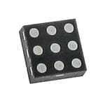
| 描述 | IC AUDIO AMP MONO 2.9W 9UTQFN |
| 产品分类 | |
| 品牌 | ISSI, Integrated Silicon Solution Inc |
| 数据手册 | |
| 产品图片 | |
| 产品型号 | IS31AP2145A-UTLS2-TR |
| rohs | 无铅 / 符合限制有害物质指令(RoHS)规范要求 |
| 产品系列 | - |
| 不同负载时的最大输出功率x通道数 | 2.9W x 1 @ 4 欧姆 |
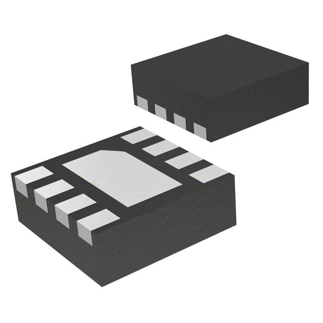
| 供应商器件封装 | 9-UTQFN(1.5x1.5) |
| 其它名称 | 706-1155-1 |
| 包装 | 剪切带 (CT) |
| 安装类型 | 表面贴装 |
| 封装/外壳 | 9-UFBGA |
| 工作温度 | -40°C ~ 85°C (TA) |
| 标准包装 | 1 |
| 特性 | AGC,无噪音,差分输入,短路保护和热保护,关断 |
| 电压-电源 | 2.7 V ~ 5.5 V |
| 类型 | D 类 |
| 输出类型 | 1-通道(单声道) |


- 商务部:美国ITC正式对集成电路等产品启动337调查
- 曝三星4nm工艺存在良率问题 高通将骁龙8 Gen1或转产台积电
- 太阳诱电将投资9.5亿元在常州建新厂生产MLCC 预计2023年完工
- 英特尔发布欧洲新工厂建设计划 深化IDM 2.0 战略
- 台积电先进制程称霸业界 有大客户加持明年业绩稳了
- 达到5530亿美元!SIA预计今年全球半导体销售额将创下新高
- 英特尔拟将自动驾驶子公司Mobileye上市 估值或超500亿美元
- 三星加码芯片和SET,合并消费电子和移动部门,撤换高东真等 CEO
- 三星电子宣布重大人事变动 还合并消费电子和移动部门
- 海关总署:前11个月进口集成电路产品价值2.52万亿元 增长14.8%


PDF Datasheet 数据手册内容提取
IS31AP2145A 2.9W@5.0V MONO CLIP-LESS & FILTER-LESS CLASS-D AUDIO POWER AMPLIFIER December 2011 GENERAL DESCRIPTION FEATURES The IS31AP2145A is a 2.9W@5.0V mono, clip-less, Filter-less Class-D architecture filter-less, high efficiency Class-D audio power AGC enable/disable function amplifier with automatic gain control. 2.9W into 4Ω at 5.0V (10% THD+N) The IS31AP2145A integrates AGC (Automatic Gain Power supply range: 2.7V to 5.5V Control) function to automatically prevent distortion of Selectable attack and release times the audio signal by which we can enhance audio Minimum external components quality and also protect the speaker from damage at High efficiency: 90% high power levels. The AGC function and its attack Click-and-pop suppression time/release time are selectable via the CTRL pin. The IS31AP2145A also provides thermal and over current Low shutdown current: 0.1μA protection functions. Short-circuit and thermal protection Space-saving UTQFN-9, 1.5mm × 1.5mm In addition to these features, 90% high efficiency, improved RF-rectification immunity, a fast start-up time and small package size make IS31AP2145A ideal APPLICATIONS choice for cellular handsets, PDAs and other portable applications. Wireless or cellular handsets and PDAs Portable navigation devices IS31AP2145A is available in a 1.5mm×1.5mm Portable DVD player UTQFN-9 package. Notebook PC Educational toys USB speakers Portable gaming TYPICAL APPLICATION CIRCUIT V Battery A2 B2 VDD VREF 1 F 1 F 0.1 F C IN A3 33nF A1 OUT+ IN+ Differential In C1 IS31AP2145A IN- C3 C IN OUT- 33nF R C2 1 CTRL1 CTRL R B1,B3 2 CTRL2 0.1 F GND R 3 Figure 1 Typical Application Circuit (Differential Input) Integrated Silicon Solution, Inc. – www.issi.com 1 Rev.A, 11/20/2011
IS31AP2145A Figure 2 Typical Application Circuit (Single-Ended Input) Integrated Silicon Solution, Inc. – www.issi.com 2 Rev.A, 11/20/2011
IS31AP2145A PIN CONFIGURATION Package Pin Configuration (Top View) UTQFN-9 PIN DESCRIPTION No. Pin Description A1 IN+ Positive input terminal. A2 VDD Power supply. A3 OUT+ Positive output terminal. B1, B3 GND Ground. B2 VREF Analog reference power supply terminal. C1 IN- Negative input terminal. C2 CTRL Power down and AGC control terminal. C3 OUT- Negative output terminal. Copyright © 2011 Integrated Silicon Solution, Inc. All rights reserved. ISSI reserves the right to make changes to this specification and its products at any time without notice. ISSI assumes no liability arising out of the application or use of any information, products or services described herein. Customers are advised to obtain the latest version of this device specification before relying on any published information and before placing orders for products. Integrated Silicon Solution, Inc. does not recommend the use of any of its products in life support applications where the failure or malfunction of the product can reasonably be expected to cause failure of the life support system or to significantly affect its safety or effectiveness. Products are not authorized for use in such applications unless Integrated Silicon Solution, Inc. receives written assurance to its satisfaction, that: a.) the risk of injury or damage has been minimized; b.) the user assume all such risks; and c.) potential liability of Integrated Silicon Solution, Inc is adequately protected under the circumstances Integrated Silicon Solution, Inc. – www.issi.com 3 Rev.A, 11/20/2011
IS31AP2145A ORDERING INFORMATION Industrial Range: -40°C to +85°C Order Part No. Package QTY/Reel IS31AP2145A-UTLS2-TR UTQFN-9, Lead-free 3000 Integrated Silicon Solution, Inc. – www.issi.com 4 Rev.A, 11/20/2011
IS31AP2145A ABSOLUTE MAXIMUM RATINGS (NOTE 1) Supply voltage, V -0.3V ~ +6.0V DD Voltage at any input pin -0.3V ~ V +0.3V DD Junction temperature, T 150°C JMAX Storage temperature range, T -65°C ~ +150°C STG Operating temperature range −40°C ~ +85°C ESD (HBM) 7kV Note: Stresses beyond those listed under “Absolute Maximum Ratings” may cause permanent damage to the device. These are stress ratings only and functional operation of the device at these or any other condition beyond those indicated in the operational sections of the specifications is not implied. Exposure to absolute maximum rating conditions for extended periods may affect device reliability. ELECTRICAL CHARACTERISTICS T = -40°C ~ +85°C, V = 2.7V ~ 5.5V, unless otherwise noted. Typical value are V = 3.6V, T = +25°C. A DD DD A Symbol Parameter Condition Min. Typ. Max. Unit V Supply voltage 2.7 5.5 V DD I Quiescent current 2 mA DD I Shutdown current V = 0V 0.1 μA SD CTRL f Switching frequency V = 2.7V ~ 5.5V 300 kHz SW DD Gain Audio input gain 18 dB AGC Characteristics V AGC1 mode setting threshold voltage 1.4 V V AGC1 DD V AGC2 mode setting threshold voltage 0.64 1.05 V AGC2 V AGC OFF mode setting threshold voltage 0.36 0.6 V OFF V Shutdown mode setting threshold voltage 0 0.14 V SD t Attack time 1 45 ms AT1 t Release time 1 2.6 s RT1 t Attack time 2 10 ms AT2 t Release time 1.2 s RT2 A Maximum attenuation gain -10 dB MAX Integrated Silicon Solution, Inc. – www.issi.com 5 Rev.A, 11/20/2011
IS31AP2145A ELECTRICAL CHARACTERISTICS AGC OFF, T = +25°C, V = 3.6V, unless otherwise noted. A DD Symbol Parameter Condition Min. Typ. Max. Unit THD+N = 10%,f = 1kHz V = 5.0V 2.90 W R = 4Ω+33µH DD L THD+N = 1%,f = 1kHz V = 5.0V 2.30 W R = 4Ω+33µH DD L P Output power O THD+N = 10%,f = 1kHz V = 5.0V 1.68 W R =8Ω +33µH DD L THD+N = 1%,f = 1kHz V = 5.0V 1.38 W R = 8Ω+33µH DD L V = 3.6V, P = 0.5W, R = 8Ω+33µH DD O L 0.165 Total harmonic f = 1kHz THD+N % distortion plus noise V = 3.6V, P = 1.0W, R = 4Ω+33µH DD O L 0.175 f = 1kHz Power supply VP-P = 200mV,RL = 8Ω,f = 217Hz -72 dB PSRR rejection ratio V = 200mV,R = 8Ω,f = 1kHz -65 dB P-P L η Maximum efficiency P = 1.0W,R = 8Ω+33µH,f = 1kHz 90 % O L t Start-up time 34 ms ST t Wake-up time 40 ms WK t Shutdown time 80 ms SD t Mode switching time 0.1 ms MOD Integrated Silicon Solution, Inc. – www.issi.com 6 Rev.A, 11/20/2011
IS31AP2145A TYPICAL PERFORMANCE CHARACTERISTICS 20 20 RL= 8Ω+33µH RL= 4Ω+33µH 10 f = 1kHz 10 f = 1kHz 5 5 ) ) % % N( 2 N( 2 VDD= 4.2V D+ VDD= 3.6V D+ H 1 H 1 T T 0.5 VDD= 4.2V 0.5 VDD= 3.6V 0.2 VDD= 5.0V 0.2 VDD= 5.0V 0.1 0.1 10m 20m 50m 100m 200m 500m 1 2 3 10m 20m 50m 100m 200m 500m 1 2 3 4 Output Power(W) Output Power(W) Figure 3 THD+N vs. Output Power Figure 4 THD+N vs. Output Power 20 20 10 VDD= 3.6V 10 VDD= 3.6V PO= 500mW PO= 1.0W RL= 8Ω+33µH RL= 4Ω+33µH 2 2 ) ) % % ( 1 ( 1 N N + + D D H H T T 0.2 0.2 0.1 0.1 0.05 0.05 0.02 0.02 0.01 0.01 20 50 100 200 500 1k 2k 5k 10k 20k 20 50 100 200 500 1k 2k 5k 10k 20k Frequency(Hz) Frequency(Hz) Figure 5 THD+N vs. Frequency Figure 6 THD+N vs. Frequency 100 100 90 90 80 80 ) 70 ) 70 % % 60 60 y( y( c c n 50 n 50 e e ci ci Effi 40 Effi 40 30 30 20 20 VDD = 3.6V~5.0V VDD = 3.6V~5.0V 10 RL = 8Ω+33μH 10 RL = 4Ω+33μH 0 0 0 0.2 0.4 0.6 0.8 1 1.2 1.4 1.6 1.8 0 0.4 0.8 1.2 1.6 2 2.4 2.8 3.2 Output Power(W) Output Power(W) Figure 7 Efficiency vs. Output Power Figure 8 Efficiency vs. Output Power Integrated Silicon Solution, Inc. – www.issi.com 7 Rev.A, 11/20/2011
IS31AP2145A 1.8 1.4 1.6 RALG=C 8 OΩF+F33µH 1.2 RALG=C 81Ω+33µH THD+N = 10% 1.4 ) ) W W 1 ( er( 1.2 THD+N = 10% wer ow 1 Po 0.8 Output P 0.8 THD+N = 1% Output 0.6 THD+N = 1% 0.6 0.4 0.4 0.2 0.2 0 0 2.5 3.5 4.5 5.0 2.5 3.5 4.5 5.0 Supply Voltage(V) Supply Voltage(V) Figure 9 Output Power vs. Supply Voltage Figure 10 Output Power vs. Supply Voltage 3 2.5 RL= 4Ω+33µH RL= 4Ω+33µH AGC OFF AGC1 2.5 THD+N = 10% 2 W) W) r( 2 THD+N = 10% er( we w 1.5 o Output Po 1.51 THD+N = 1% Output P 1 THD+N = 1% 0.5 0.5 0 0 2.5 3.5 4.5 5.0 2.5 3.5 4.5 5.0 Supply Voltage(V) Supply Voltage(V) Figure 11 Output Power vs. Supply Voltage Figure 12 Output Power vs. Supply Voltage +0 VDD= 3.6V, 4.2V -20 RL= 8Ω+33μH -40 ) B d R( -60 R S P -80 -100 -120 20 50 100 200 500 1k 2k 5k 10k 20k Frequency(Hz) Figure 13 PSRR vs. Frequency Integrated Silicon Solution, Inc. – www.issi.com 8 Rev.A, 11/20/2011
IS31AP2145A APPLICATION INFORMATION DIGITAL AMPLIFIER AGC (AUTOMATIC GAIN CONTROL) CONTROL FUNCTION The IS31AP2145A is a 2.9W@5.0V mono, clip-less, filter-less, high efficiency Class-D audio power This is the function to control the output in order to amplifier with automatic gain control. obtain a maximum output level without distortion when an excessive input is applied which would otherwise The IS31AP2145A integrates AGC (Automatic Gain cause clipping at the differential signal output. That is, Control) function to automatically prevent distortion of with the AGC function, IS31AP2145A lowers the gain the audio signal by which we can enhance audio of the digital amplifier to an appropriate value so as not quality and also protect speaker from damage at high to cause clipping at the differential signal output power levels. In addition, IS31AP2145A has been (Figure 14). designed so that high-efficiency can be maintained within an average power range that is used for mobile terminal. Figure 14 Operation of AGC Function Integrated Silicon Solution, Inc. – www.issi.com 9 Rev.A, 11/20/2011
IS31AP2145A The attack time and the release time of AGC control Table 2 Mode Setting have two levels (refer to Table 1). They are selected by CTRL1 CTRL2 Mode the voltage at the CTRL terminal (refer to Table 2). The attack time is a time interval that gain falls from 18dB H H AGC1 to 10dB with a big signal input enough. And the release H GND AGC2 time is a time from target attenuation to no AGC attenuation. GND H AGC OFF Table 1 Attack Time and Release Time GND GND Shutdown “H” level indicates a microcomputer’s I/O port H level AGC Mode Attack Time Release Time output voltage that is input to CTRL1 and CTRL2 AGC1 terminals and GND indicates GND of the 45ms 2.6s (Recommended) microcomputer. AGC2 10ms 1.2s GND level of the microcomputer must be the same as Assuming no limitation by the power supply, the audio that of IS31AP2145A. output signal would be as in Figure 15. The control of CTRL terminal is based on I/O port H level output voltage of microcomputer that is connected. Set resistance constants according to I/O port H level Figure 15 Assuming no Restriction from Power Supply, the Audio output voltage of each microcomputer as Table 3 Output Signal below. In normal operation without the AGC, the output is Table 3 Resistors Setting distorted because of the restriction from power supply, V 1.8V 2.6V 2.8V 3.0V 3.3V 5.0V as shown in Figure 16. I/O R1 27kΩ 33kΩ 33kΩ 33kΩ 33kΩ 56kΩ R2 56kΩ 68kΩ 68kΩ 68kΩ 68kΩ 120kΩ R3 82kΩ 27kΩ 24kΩ 22kΩ 18kΩ 15kΩ Functions of CTRL pin are designed with their control Figure 16 AGC Function Off by two control pins (CTRL1 and CTRL3). Only a With the AGC function of IS31AP2145A, the optimum switching control between AGC1 Mode and Shutdown output power can be obtained along with the minimal Mode is available when a single control terminal is distortion. The Figure 17 shows the outcome of AGC used (Table 4 and Figure 19). function. Attack Time Release Time Figure 17 AGC Function On Figure 19 AGC1 Mode Circuit CTRL TERMINAL FUNCTION Table 4 Mode Setting By setting the threshold voltage of each mode to CTRL CTRL1 Mode terminal, the followings can be set: AGC1, AGC2, AGC OFF, and Shutdown Mode (Table 2 and Figure 18). H AGC1 GND Shutdown SYSTEM TIMING The CTRL terminal should be configured as the Figure 20. When in the Shutdown Mode, the level of the terminal must not be changed from GND level during t . When the IS31AP2145A wakes up, the CTRL Figure 18 AGC Function Mode Setting SD terminal must be set to H level first, then enter the setting mode. Integrated Silicon Solution, Inc. – www.issi.com 10 Rev.A, 11/20/2011
IS31AP2145A Figure 20 System Timing INPUT CAPACITORS (C ) DECOUPLING CAPACITOR (C ) IN S The input capacitors (C ) and internal resistor (R = The IS31AP2145A is a high performance class-D IN IN 28.5kΩ) form a high-pass filter with the corner audio amplifier that requires adequate power supply frequency, f , determined in Equation (1). decoupling to ensure the efficiency is high and total C harmonic distortion (THD) is low. For higher frequency 1 transients, spikes, or digital hash on the line, a good f (1) c 2R C low equivalent-series-resistance (ESR) ceramic IN IN capacitor, typically 0.1μF, placed as close as possible For example, in figure 1, to the device VDD lead works best. Placing this CIN = 33nF, RIN = 28.5kΩ, decoupling capacitor close to the IS31AP2145A is very 1 important for the efficiency of the class-D amplifier, So, f 169Hz because any resistance or inductance in the trace c 228.5k33nF between the device and the capacitor can cause a loss The capacitors should have a tolerance of 10% or in efficiency. For filtering lower frequency noise signals, better, because any mismatch in capacitance causes a 1μF or greater capacitor placed near the audio power an impedance mismatch at the corner frequency and amplifier would also help. below. Integrated Silicon Solution, Inc. – www.issi.com 11 Rev.A, 11/20/2011
IS31AP2145A CLASSIFICATION REFLOW PROFILES Profile Feature Pb-Free Assembly Preheat & Soak 150°C Temperature min (Tsmin) 200°C Temperature max (Tsmax) 60-120 seconds Time (Tsmin to Tsmax) (ts) Average ramp-up rate (Tsmax to Tp) 3°C/second max. Liquidous temperature (TL) 217°C Time at liquidous (tL) 60-150 seconds Peak package body temperature (Tp)* Max 260°C Time (tp)** within 5°C of the specified Max 30 seconds classification temperature (Tc) Average ramp-down rate (Tp to Tsmax) 6°C/second max. Time 25°C to peak temperature 8 minutes max. Figure 21 Classification Profile Integrated Silicon Solution, Inc. – www.issi.com 12 Rev.A, 11/20/2011
IS31AP2145A TAPE AND REEL INFORMATION Note: All dimensions in millimeters unless otherwise stated. Integrated Silicon Solution, Inc. – www.issi.com 13 Rev.A, 11/20/2011
IS31AP2145A PACKAGING INFORMATION UTQFN-9 Integrated Silicon Solution, Inc. – www.issi.com 14 Rev.A, 11/20/2011
Mouser Electronics Authorized Distributor Click to View Pricing, Inventory, Delivery & Lifecycle Information: I SSI: IS31AP2145A-UTLS2-TR