ICGOO在线商城 > 集成电路(IC) > 线性 - 音頻放大器 > TAS5613APHDR
 Datasheet下载
- 型号: TAS5613APHDR
- 制造商: Texas Instruments
- 库位|库存: xxxx|xxxx
- 要求:
| 数量阶梯 | 香港交货 | 国内含税 |
| +xxxx | $xxxx | ¥xxxx |
查看当月历史价格
查看今年历史价格
TAS5613APHDR产品简介:
ICGOO电子元器件商城为您提供TAS5613APHDR由Texas Instruments设计生产,在icgoo商城现货销售,并且可以通过原厂、代理商等渠道进行代购。 TAS5613APHDR价格参考¥79.60-¥101.28。Texas InstrumentsTAS5613APHDR封装/规格:线性 - 音頻放大器, Amplifier IC 1-Channel (Mono) or 2-Channel (Stereo) Class D 64-HTQFP (14x14)。您可以下载TAS5613APHDR参考资料、Datasheet数据手册功能说明书,资料中有TAS5613APHDR 详细功能的应用电路图电压和使用方法及教程。
TAS5613APHDR是德州仪器(Texas Instruments)推出的一款高效D类音频功率放大器,属于线性-音频放大器类别。该器件主要面向需要高效率、高输出功率和优良音质的音频应用场合。

典型应用场景包括:
家用与高端音响系统:适用于家庭影院、有源音箱和多媒体音响,提供高保真音频输出,支持多通道配置,提升声音表现力。
专业音频设备:用于便携式扩音系统、舞台监听音箱和会议系统,具备高功率密度和低失真特性,适合对音质要求较高的环境。
消费类电子产品:如智能电视、Soundbar(条形音响)和游戏音响系统,其高效率可减少发热,节省空间并提高系统可靠性。
工业与商业音频系统:适用于公共广播系统、零售店背景音乐系统等需长时间稳定运行的场景。

TAS5613APHDR采用BTL(桥接负载)输出结构,支持高达500W的峰值输出功率(在8Ω负载下),具备良好的热管理和过流、过温保护功能,确保系统安全。其HDR(高动态范围)设计进一步提升了音频动态表现,适合追求高清晰度与强驱动能力的应用需求。

综上,TAS5613APHDR广泛应用于对功率、效率和音质均有较高要求的中高端音频系统中。
| 参数 | 数值 |
| 产品目录 | 集成电路 (IC) |
| 描述 | IC AMP AUDIO 150W STER D 64HTQFP |
| 产品分类 | |
| 品牌 | Texas Instruments |
| 数据手册 | |
| 产品图片 |
|
| 产品型号 | TAS5613APHDR |
| PCN组件/产地 | |
| rohs | 无铅 / 符合限制有害物质指令(RoHS)规范要求 |
| 产品系列 | PurePath™ HD |
| 不同负载时的最大输出功率x通道数 | 300W x 1 @ 2 欧姆; 200W x 2 @ 3 欧姆 |
| 供应商器件封装 | 64-HTQFP(14x14) |
| 其它名称 | 296-27616-6 |
| 包装 | Digi-Reel® |
| 安装类型 | 表面贴装 |
| 封装/外壳 | 64-TQFP 裸露焊盘 |
| 工作温度 | 0°C ~ 70°C (TA) |
| 标准包装 | 1 |
| 特性 | 消除爆音,差分输入,短路和热保护,关闭 |
| 电压-电源 | 18 V ~ 38 V |
| 类型 | D 类 |
| 输出类型 | 1-通道(单声道)或 2-通道(立体声) |


- 商务部:美国ITC正式对集成电路等产品启动337调查
- 曝三星4nm工艺存在良率问题 高通将骁龙8 Gen1或转产台积电
- 太阳诱电将投资9.5亿元在常州建新厂生产MLCC 预计2023年完工
- 英特尔发布欧洲新工厂建设计划 深化IDM 2.0 战略
- 台积电先进制程称霸业界 有大客户加持明年业绩稳了
- 达到5530亿美元!SIA预计今年全球半导体销售额将创下新高
- 英特尔拟将自动驾驶子公司Mobileye上市 估值或超500亿美元
- 三星加码芯片和SET,合并消费电子和移动部门,撤换高东真等 CEO
- 三星电子宣布重大人事变动 还合并消费电子和移动部门
- 海关总署:前11个月进口集成电路产品价值2.52万亿元 增长14.8%


PDF Datasheet 数据手册内容提取
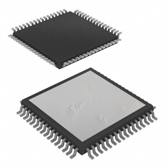
TAS5613A PurePath Digital www.ti.com SLAS711B–JUNE2010–REVISEDSEPTEMBER2011 150W STEREO / 300W MONO PurePath™ HD ANALOG-INPUT POWER STAGE CheckforSamples:TAS5613A FEATURES • ThermallyEnhancedPackageOptions: 1 • ActiveEnabledIntegratedFeedbackProvides: – PHD(64-pinQFP) 23 (PurePath™HD) – DKD(44-pinPSOP3) – SignalBandwidthupto80kHzforHigh APPLICATIONS FrequencyContentFromHDSources – UltraLow0.03%THDat1Winto4Ω • HomeTheaterSystems – FlatTHDatallFrequenciesforNatural • AVReceivers Sound • DVD/Blu-rayDisk™Receivers – 80dBPSRR(BTL,NoInputSignal) • MiniComboSystems – >100dB(AWeighted)SNR • ActiveSpeakersandSubwoofers – ClickandPopFreeStartupandStop DESCRIPTION • PincompatiblewithTAS5630,TAS5615and TAS5611 The TAS5613A is a high-performance analog input Class D amplifier with integrated closed loop • MultipleConfigurationsPossibleontheSame feedback technology (known as PurePath™ HD). It PCB: has the ability to drive up to 150 W.(1) Stereo into 4Ω – MonoParallelBridgeTiedLoad(PBTL) speakersfromasingle36Vsupply. – StereoBridgeTiedLoad(BTL) PurePath™ HD technology enables traditional – 2.1SingleEnded(SE)StereoPairand AB-Amplifier performance (<0.03% THD) levels while BridgeTiedLoadSubwoofer providing the power efficiency of traditional class D • TotalOutputPowerat10%THD+N amplifiers. – 300WinMonoPBTLConfiguration Unlike traditional Class-D amplifiers, the distortion curve only increases once the output levels move into – 150WperChannelinStereoBTL clipping. Configuration • TotalOutputPowerinBTLConfigurationat PurePath™ HD technology enables lower idle losses makingthedeviceevenmoreefficient. 1%THD+N – 160WStereointo3Ω TTOOTTAALLHHAARRMMOONNIICCDDIISSTTOORRTTIIOONN++NNOOIISSEE VVSS – 125WStereointo4Ω OOUUTTPPUUTTPPOOWWEERR 1100 – 85WStereointo6Ω 4444OOOOhhhhmmmm((((6611kkkkHHHHzzzz)))) TCTCCCOONN==FF77II55GGCC==BBTTLL %% • –>906%5WEfSficteierenotPinotwoe8rΩStageWith60-mΩ Distortion-Distortion- 11 OutputMOSFETs monicmonic 00,,11 • Self-ProtectionDesign(Including HarHar Undervoltage,Overtemperature,Clipping,and talTotal ShortCircuitProtection)WithErrorReporting D+N- 0,01 H • EMICompliantWhenUsedWith T RecommendedSystemDesign 0,001 0,01 1 100 PO-OutputPower-W (1) Achievableoutputpowerlevelsaredependentonthethermal configurationofthetargetapplication.Ahighperformance thermalinterfacematerialbetweenthepackageexposed heatslugandtheheatsinkshouldbeusedtoachievehigh outputpowerlevels 1 Pleasebeawarethatanimportantnoticeconcerningavailability,standardwarranty,anduseincriticalapplicationsofTexas Instrumentssemiconductorproductsanddisclaimerstheretoappearsattheendofthisdatasheet. Blu-rayDiskisatrademarkofBlu-rayDiscAssociation. 2 Allothertrademarksarethepropertyoftheirrespectiveowners. 3 UNLESS OTHERWISE NOTED this document contains Copyright©2010–2011,TexasInstrumentsIncorporated PRODUCTION DATA information current as of publication date. Products conform to specifications per the terms of Texas Instruments standard warranty. Production processing does not necessarilyincludetestingofallparameters.
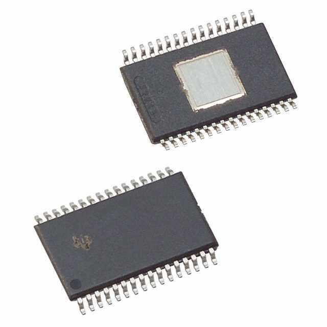
TAS5613A SLAS711B–JUNE2010–REVISEDSEPTEMBER2011 www.ti.com Thesedeviceshavelimitedbuilt-inESDprotection.Theleadsshouldbeshortedtogetherorthedeviceplacedinconductivefoam duringstorageorhandlingtopreventelectrostaticdamagetotheMOSgates. DEVICE INFORMATION Pin Assignment TheTAS5613Aisavailableintwothermallyenhancedpackages: • 64-PinQFP(PHD)PowerPackage • 44-PinPSOP3Package(DKD) The package type contains a heat slug that is located on the top side of the device for convenient thermal couplingtotheheatsink. PHD PACKAGE DKD PACKAGE (TOPVIEW) (TOPVIEW) VDDPSU_REFNCNCNCNCGNDGNDGVDD_BGVDD_ABST_AOUT_AOUT_APVDD_APVDD_AGND_A PSU_REF 1 44 GVDD_AB VDD 2 43 BST_A OC_ADJ 3 42 PVDD_A ORCE_SAEDTJ 21646362616059585756555453525150494478 GGNNDD__AB C_STARRETSUEPT 45 4410 OPVUDTD_A_A C_STARTUP 3 46 GND_B INPUT_A 6 39 OUT_A INPUT_A 4 45 OUT_B INPUT_B 7 38 GND_A INPUT_B 5 44 OUT_B VI_CM 8 37 GND_B VI_CM 6 43 PVDD_B INPAVUGGRTNNE_CDGD 19870 34449012 PBBPVSSVDTTD__DDCB__CB AVGGRNNEDGD 91110 (TOP44pinsP 333654 OBPSVUTDT_D_BB_B FRINEPQU_AT_DDJ 1112 3378 OPVUDT_DC_C IINNPPUUTT__DC 1132 VIEWACK 3332 BPSVTD_DC_C OSC_IO+ 13 36 OUT_C FREQ_ADJ 14 )AG 31 OUT_C OSC_IO- 14 35 GND_C E SD 15 64-pins QFPpackage 34 GND_C OSC_IO+ 15 30 GND_C OTW1 16 33 GND_D OSC_IO- 16 29 GND_D 17181920212223242526272829303132 SD 17 28 OUT_D OTW 18 27 OUT_D READY 19 26 PVDD_D OTW2CLIPREADYM1M2M3GNDGNDVDD_CVDD_DBST_DOUT_DOUT_DVDD_DVDD_DGND_D MM21 2201 2254 PBVSDT_DD_D GG PP M3 22 23 GVDD_CD PIN ONE LOCATION PHD PACKAGE Electrical Pin 1 Pin 1 Marker White Dot 2 Copyright©2010–2011,TexasInstrumentsIncorporated
TAS5613A www.ti.com SLAS711B–JUNE2010–REVISEDSEPTEMBER2011 MODE SELECTION PINS MODEPINS ANALOG OUTPUT DESCRIPTION M3 M2 M1 INPUT CONFIGURATION 0 0 0 Differential 2×BTL ADmode 0 0 1 — — Reserved 0 1 0 Differential 2×BTL BDmode Differential (BTL) 0 1 1 1×BTL+2×SE BTL=BDmode,SE=ADmode SingleEnded (SE) 1 0 0 SingleEnded 4×SE ADmode INPUT_C(1) INPUT_D(1) 1 0 1 Differential 1×PBTL 0 0 ADmode 1 0 BDmode 1 1 0 Reserved 1 1 1 (1) INPUT_CandDareusedtoselectbetweenasubsetofADandBDmodeoperationsinPBTLmode(1=VREGand0=GND). PACKAGE HEAT DISSIPATION RATINGS (1) PARAMETER TAS5613APHD TAS5613ADKD R (°C/W)–2BTLor4SEchannels 3.2 2.1 θJC R (°C/W)–1BTLor2SEchannel(s) 5.4 3.5 θJC R (°C/W)–1SEchannel 7.9 5.1 θJC PadArea (2) 64mm2 80mm2 (1) J isjunction-to-case,CHiscase-to-heatsink C (2) R isanimportantconsideration.Assumea2-milthicknessoftypicalthermalgreasebetweenthepadareaandtheheatsinkandboth θH channelsactive.TheR withthisconditionis1.22°C/WforthePHDpackageand1.02°C/WfortheDKDpackage. θCH Table1. ORDERINGINFORMATION (1) T PACKAGE DESCRIPTION A TAS5613APHD 64pinHTQFP 0°C–70°C TAS5613ADKD 44pinPSOP3 (1) Forthemostcurrentpackageandorderinginformation,seethePackageOptionAddendumattheendofthisdocument,orseetheTI websiteatwww.ti.com. Copyright©2010–2011,TexasInstrumentsIncorporated 3
TAS5613A SLAS711B–JUNE2010–REVISEDSEPTEMBER2011 www.ti.com ABSOLUTE MAXIMUM RATINGS overoperatingfree-airtemperaturerangeunlessotherwisenoted (1) TAS5613A UNIT VDDtoGND –0.3to13.2 V GVDDtoGND –0.3to13.2 V PVDD_XtoGND_X(2) –0.3to53 V OUT_XtoGND_X(2) –0.3to53 V BST_XtoGND_X(2) –0.3to66.2 V BST_XtoGVDD_X(2) –0.3to53 V VREGtoGND –0.3to4.2 V GND_XtoGND –0.3to0.3 V GNDtoAGND –0.3to0.3 V OC_ADJ,M1,M2,M3,OSC_IO+,OSC_IO–,FREQ_ADJ,VI_CM,C_STARTUP, –0.3to4.2 V PSU_REFtoGND INPUT_X –0.3to7 V RESET,SD,OTW,OTW1,OTW2,CLIP,READYtoGND –0.3to7 V Continuoussinkcurrent(SD,OTW,OTW1,OTW2,CLIP,READY) 9 mA Operatingjunctiontemperaturerange,T 0to150 °C J Storagetemperature,T –40to150 °C stg Human-BodyModel(3)(allpins) ±2 kV Electrostaticdischarge Charged-DeviceModel(3)(allpins) ±500 V (1) StressesbeyondthoselistedunderAbsoluteMaximumRatingsmaycausepermanentdamagetothedevice.Thesearestressratings only,andfunctionaloperationofthedeviceattheseoranyotherconditionsbeyondthoseindicatedunderRecommendedOperating Conditionsisnotimplied.Exposuretoabsolute-maximum-ratedconditionsforextendedperiodsmayaffectdevicereliability. (2) ThesevoltagesrepresentstheDCvoltage+peakACwaveformmeasuredattheterminalofthedeviceinallconditions. (3) Failuretofollowgoodanti-staticESDhandlingduringmanufactureandreworkwillcontributetodevicemalfunction.Makesurethe operatorshandlingthedeviceareadequatelygroundedthroughtheuseofgroundstrapsoralternativeESDprotection. 4 Copyright©2010–2011,TexasInstrumentsIncorporated
TAS5613A www.ti.com SLAS711B–JUNE2010–REVISEDSEPTEMBER2011 RECOMMENDED OPERATING CONDITIONS overoperatingfree-airtemperaturerange(unlessotherwisenoted) MIN TYP MAX UNIT PVDD_x Half-bridgesupply DCsupplyvoltage 18 36 38 V Supplyforlogicregulatorsand GVDD_x DCsupplyvoltage 10.8 12 13.2 V gate-drivecircuitry VDD Digitalregulatorsupplyvoltage DCsupplyvoltage 10.8 12 13.2 V R (BTL) 3.5 4 L OutputfilteraccordingtoFigure12and R (SE) Loadimpedance 2.8 3 Ω L Figure13 R (PBTL) 1.6 2 L OutputfilteraccordingtoFigure12+ R (BTL) Loadimpedance 2.8 3 Ω L Schottky,R =22kΩ OC L (BTL) 7 10 OUT L (SE) Outputfilterinductance MinimumoutputinductanceatI 7 15 μH OUT OC L (PBTL) 7 10 OUT Nominal 385 400 415 PWMframerateselectableforAM F interferenceavoidance;1% AM1 315 333 350 kHz PWM Resistortolerance AM2 260 300 335 Nominal;Mastermode 9.9 10 10.1 PWMframerateprogramming R AM1;Mastermode 19.8 20 20.2 kΩ FREQ_ADJ resistor AM2;Mastermode 29.7 30 30.3 C PVDDclosedecouplingcapacitors 2.0 μF PVDD R Over-currentprogrammingresistor Resistortolerance=5% 22 30 kΩ OC R Over-currentprogrammingresistor Resistortolerance=5% 47 64 kΩ OC_LATCHED VoltageonFREQ_ADJpinfor V Slavemode 3.3 V FREQ_ADJ slavemodeoperation T Junctiontemperature 0 125 °C J PINFUNCTIONS PIN FUNCTION(1) DESCRIPTION NAME PHDNO. DKDNO. AGND 8 10 P Analogground BST_A 54 43 P HSbootstrapsupply(BST),external0.033μFcapacitortoOUT_Arequired. BST_B 41 34 P HSbootstrapsupply(BST),external0.033μFcapacitortoOUT_Brequired. BST_C 40 33 P HSbootstrapsupply(BST),external0.033μFcapacitortoOUT_Crequired. BST_D 27 24 P HSbootstrapsupply(BST),external0.033μFcapacitortoOUT_Drequired. CLIP 18 – O Clippingwarning;opendrain;activelow C_STARTUP 3 5 O Startupramprequiresachargingcapacitorof4.7nFtoGND FREQ_ADJ 12 14 I PWMframerateprogrammingpinrequiresresistortoGND 7,23,24, GND 9 P Ground 57,58 GND_A 48,49 38 P Powergroundforhalf-bridgeA GND_B 46,47 37 P Powergroundforhalf-bridgeB GND_C 34,35 30 P Powergroundforhalf-bridgeC GND_D 32,33 29 P Powergroundforhalf-bridgeD GVDD_A 55 – P Gatedrivevoltagesupplyrequires0.1μFcapacitortoGND_A GVDD_B 56 – P Gatedrivevoltagesupplyrequires0.1μFcapacitortoGND_B GVDD_C 25 – P Gatedrivevoltagesupplyrequires0.1μFcapacitortoGND_C GVDD_D 26 - P Gatedrivevoltagesupplyrequires0.1uFcapacitortoGND_D GVDD_AB – 44 P Gatedrivevoltagesupplyrequires0.22μFcapacitortoGND_A/GND_B GVDD_CD – 23 P Gatedrivevoltagesupplyrequires0.22μFcapacitortoGND_C/GND_D (1) I=Input,O=Output,P=Power Copyright©2010–2011,TexasInstrumentsIncorporated 5
TAS5613A SLAS711B–JUNE2010–REVISEDSEPTEMBER2011 www.ti.com PINFUNCTIONS(continued) PIN FUNCTION(1) DESCRIPTION NAME PHDNO. DKDNO. INPUT_A 4 6 I InputsignalforhalfbridgeA INPUT_B 5 7 I InputsignalforhalfbridgeB INPUT_C 10 12 I InputsignalforhalfbridgeC INPUT_D 11 13 I InputsignalforhalfbridgeD M1 20 20 I Modeselection M2 21 21 I Modeselection M3 22 22 I Modeselection NC 59-62 – – Noconnect,pinsmaybegrounded. OC_ADJ 1 3 O Analogovercurrentprogrammingpinrequires30kΩresistortoground: OSC_IO+ 13 15 I/O Oscillatormaster/slaveoutput/input. OSC_IO– 14 16 I/O Oscillatormaster/slaveoutput/input. /OTW - 18 O Overtemperaturewarningsignal,opendrain,activelow. OTW1 16 – O Overtemperaturewarningsignal,opendrain,activelow. OTW2 17 – O Overtemperaturewarningsignal,opendrain,activelow. OUT_A 52,53 39,40 O Output,halfbridgeA OUT_B 44,45 36 O Output,halfbridgeB OUT_C 36,37 31 O Output,halfbridgeC OUT_D 28,29 27,28 O Output,halfbridgeD PSU_REF 63 1 P PSUReferencerequiresclosedecouplingof330pFtoGND PowersupplyinputforhalfbridgesArequiresclosedecouplingof2μFcapacitorto PVDD_A 50,51 41,42 P GND_A. PowersupplyinputforhalfbridgesBrequiresclosedecouplingof2μFcapacitorto PVDD_B 42,43 35 P GND_B. PowersupplyinputforhalfbridgesCrequiresclosedecouplingof2μFcapacitorto PVDD_C 38,39 32 P GND_C. PowersupplyinputforhalfbridgesDrequiresclosedecouplingof2μFcapacitorto PVDD_D 30,31 25,26 P GND_D. READY 19 19 O Normaloperation;opendrain;activehigh RESET 2 4 I DeviceresetInput;activelow,requires47kΩpullupresistortoVREG SD 15 17 O Shutdownsignal,opendrain,activelow Powersupplyforinternalvoltageregulatorrequiresa10-μFcapacitorwitha0.1-μF VDD 64 2 P capacitortoGNDfordecoupling. VI_CM 6 8 O Analogcomparatorreferencenoderequiresclosedecouplingof1nFtoGND VREG 9 11 P Internalregulatorsupplyfilterpinrequires0.1-μFcapacitortoGND 6 Copyright©2010–2011,TexasInstrumentsIncorporated
TAS5613A www.ti.com SLAS711B–JUNE2010–REVISEDSEPTEMBER2011 TYPICAL SYSTEM BLOCK DIAGRAM Capsfor External System microcontroller Filtering or & Analog circuitry Startup/Stop (2) SynOchscroilnlaiztoartion OOSSCC__SDIIOO+- RESET OTW1 OTW2 OT,,W CLIP READY VI_CM PSU_REF C_STARTUP BBSSTT__AB BoCoatsptsrap INPUT_A OUT_A 2ndOrder ANALOG_IN_A Input DC Input Output L-C Output Blocking INPUT_B H-Bridge1 H-Bridge1 OUT2_B Filter for ANALOG_IN_B Caps each 2 H-Bridge Hardwire 2-CHANNEL PWM Frame RateAdjust H-BRIDGE FREQ_ADJ & BTL MODE Master/Slave Mode 2ndOrder ANALOG_IN_C Input DC INPUT_C Input Output OUT_C L-C Output ANALOG_IN_D BlCoackpisng INPUT_D H-Bridge2 H-Bridge2 OUT2_D Fieltaecr hfor 2 H-Bridge HCaMorodndwtreoirle MMM213 PVDD_A,B,C,D GND_A,B,C,D GVDD_A,B,C,D GND VDD VREG AGND OC_ADJ BBSSTT__CD BoCoatsptsrap 8 8 4 PVDD PVDD GVDD,VDD, Hardwire 36V Power Supply &VREG Over- SYSTEM Decoupling Power Supply Current Power Decoupling Limit Supplies GND GND GVDD(12V)/VDD(12V) 12V VAC Copyright©2010–2011,TexasInstrumentsIncorporated 7
TAS5613A SLAS711B–JUNE2010–REVISEDSEPTEMBER2011 www.ti.com FUNCTIONAL BLOCK DIAGRAM CLIP READY OTW1 OTW2 SD MMM123 &I/OLOGIC VDD RESET PROTECTION PORTWEEESMREP-TUP GVDD_A UVP GVDD_C VREG AVRGENGD C_STARTUP CSOTANRTTRUOPL SENSE GVDD_B GVDD_D GND PORVOETRE-LCOTAIODN CB3C CUSERNRSEENT OC_ADJ OSC_SYNC_IO+ OSC_SYNC_IO- OSCILLATOR PPSC 44 POVUDTD_X_X FREQ_ADJ 4 GND_X GVDD_A PWM PSU_REF PSU_FF GPVNDDD_X DAECTTEICVITTOYR BST_A VI_CM PVDD_A REPCWEIMVER CONTROL COTINMTINRGOL GATE-DRIVE OUT_A GND_A GVDD_B ANALOG - BST_B INPUT_A LOOPFILTER + PVDD_B ANALOG + REPCWEIMVER CONTROL COTINMTINRGOL GATE-DRIVE OUT_B INPUT_B LOOPFILTER - INPUT_C LOAONPAFLIOLTGER ANALOG INPUT MUX +- ANALOG COMPARATOR MUX REPCWEIMVER CONTROL COTINMTINRGOL GATE-DRIVE GGOPBVSNVUDTDDT_D_D_CCB__CC INPUT_D ANALOG + GND_C LOOPFILTER - GVDD_D BST_D PVDD_D REPCWEIMVER CONTROL COTINMTINRGOL GATE-DRIVE OUT_D GND_D 8 Copyright©2010–2011,TexasInstrumentsIncorporated
TAS5613A www.ti.com SLAS711B–JUNE2010–REVISEDSEPTEMBER2011 AUDIO CHARACTERISTICS (BTL) PCBandsystemconfigurationareinaccordancewithrecommendedguidelines.Audiofrequency=1kHz,PVDD_X=36V, GVDD_X=12V,R =4Ω,f =400kHz,R =30kΩ,T =75°C,OutputFilter:L =7μH,C =680nF,mode=010, L S OC C DEM DEM unlessotherwisenoted. PARAMETER TESTCONDITIONS MIN TYP MAX UNIT R =3Ω,10%THD+N(R =22kΩ,add L OC 200 SchottkydiodesfromOUT_XtoGND_X) R =4Ω,10%THD+N 150 L P Poweroutputperchannel W O R =3Ω,1%THD+N(R =22kΩ,add L OC 160 SchottkydiodesfromOUT_XtoGND_X) R =4Ω,1%THD+N 125 L THD+N Totalharmonicdistortion+noise 1W 0.03% A-weighted,AES17filter,InputCapacitor V Outputintegratednoise 185 μV n Grounded |V | Outputoffsetvoltage InputsACcoupledtoGND 8 25 mV OS SNR Signal-to-noiseratio(1) 100 dB DNR Dynamicrange 100 dB P PowerdissipationduetoIdlelosses(I ) P =0,4channelsswitching(2) 1.8 W idle PVDD_X O (1) SNRiscalculatedrelativeto1%THD+Noutputlevel. (2) Actualsystemidlelossesalsoareaffectedbycorelossesofoutputinductors. AUDIO CHARACTERISTICS (PBTL) PCBandsystemconfigurationareinaccordancewithrecommendedguidelines.Audiofrequency=1kHz,PVDD_X=36V, GVDD_X=12V,R =2Ω,f =400kHz,R =30kΩ,T =75°C,OutputFilter:L =7μH,C =680nF,MODE=101-BD, L S OC C DEM DEM unlessotherwisenoted. PARAMETER TESTCONDITIONS MIN TYP MAX UNIT R =2Ω,10%THD+N 300 L R =3Ω,10%THD+N 200 L R =4Ω,10%THD+N 160 L P Poweroutputperchannel W O R =2Ω,1%THD+N 250 L R =3Ω,1%THD+N 160 L R =4Ω,1%THD+N 130 L THD+N Totalharmonicdistortion+noise 1W 0.05% V Outputintegratednoise A-weighted 182 μV n SNR Signaltonoiseratio(1) A-weighted 100 dB DNR Dynamicrange A-weighted 100 dB P Powerdissipationduetoidlelosses(IPVDD_X) P =0,4channelsswitching(2) 1.8 W idle O (1) SNRiscalculatedrelativeto1%THD+Noutputlevel. (2) Actualsystemidlelossesareaffectedbycorelossesofoutputinductors. Copyright©2010–2011,TexasInstrumentsIncorporated 9
TAS5613A SLAS711B–JUNE2010–REVISEDSEPTEMBER2011 www.ti.com ELECTRICAL CHARACTERISTICS PVDD_X=36V,GVDD_X=12V,VDD=12V,T (Casetemperature)=75°C,f =400kHz,unlessotherwisespecified. C S PARAMETER TESTCONDITIONS MIN TYP MAX UNIT INTERNALVOLTAGEREGULATORANDCURRENTCONSUMPTION VREG Voltageregulator,onlyusedasreferencenode VDD=12V 3 3.3 3.6 V Analogcomparatorreferencenode,VI_CM 1.5 1.75 1.9 V Operating,50%dutycycle 20 IVDD VDDsupplycurrent mA Idle,resetmode 20 50%dutycycle 10 IGVDD_x Gate-supplycurrentperhalf-bridge mA Resetmode 1.5 50%dutycyclewithrecommendedoutputfilter 12.5 mA IPVDD_x Half-bridgeidlecurrent Resetmode,Noswitching 620 μA ANALOGINPUTS RIN Inputresistance READY=HIGH 33 kΩ VIN Maximuminputvoltageswing 7 V IIN Maximuminputcurrent 1 mA G InvertingvoltageGain,(VOUT/VIN) 21 dB OSCILLATOR Nominal,MasterMode 3.85 4 4.15 fOSC_IO+ AM1,MasterMode FPWM×10 3.15 3.33 3.5 MHz AM2,MasterMode 2.6 3 3.35 VIH Highlevelinputvoltage 1.86 V VIL Lowlevelinputvoltage 1.45 V OUTPUT-STAGEMOSFETs RDS(on) DDrraaiinn--ttoo--ssoouurrcceerreessiissttaannccee,,lhoiwghssididee(L(HSS)) TGJV=D2D5=°C1,2IVncludesmetallizationresistance, 6600 110000 mmΩΩ I/OPROTECTION Undervoltageprotectionlimit,GVDD_xand Vuvp,G VDD 9.5 V Vuvp,hyst(1) 0.6 V Overtemperaturewarning1,OTW1(1) 95 100 105 °C OTW Overtemperaturewarning2,OTW,OTW2(1) 115 125 135 °C TemperaturedropneededbelowOTW OTWHYST(1) temperatureforOTWtobeinactiveafterOTW 25 °C event. OTE(1) Overtemperatureerror 145 155 165 °C O(1)TE-OTWdifferential OTE-OTWdifferential 30 °C OTEHYST(1) AfolrloewseintgneaendOsTtoEoecvceunrtforSDtobereleased 25 °C OLPC Overloadprotectioncounter fPWM=400kHz 2.6 ms Resistor–programmable,nominalpeakcurrentin 14 1Ωload,ROCP=30kΩ IOC Overcurrentlimitprotection Resistor–programmable,nominalpeakcurrentin A 1Ωload,ROCP=22kΩ(withSchottkydiodeson 18 outputnodes) Resistor–programmable,peakcurrentin1Ωload, 14 ROCP=64kΩ IOC_LATCHED Overcurrentlimitprotection Resistor–programmable,nominalpeakcurrentin A 1Ωload,ROCP=47kΩ(withSchottkydiodeson 18 outputnodes) Timefromswitchingtransitiontoflip-stateinduced IOCT Overcurrentresponsetime byovercurrent. 150 ns ConnectedwhenRESETisactivetoprovide IPD Outputpulldowncurrentofeachhalf bootstrapcharge.NotusedinSEmode. 3 mA (1) Specifiedbydesign. 10 Copyright©2010–2011,TexasInstrumentsIncorporated
TAS5613A www.ti.com SLAS711B–JUNE2010–REVISEDSEPTEMBER2011 ELECTRICAL CHARACTERISTICS (continued) PVDD_X=36V,GVDD_X=12V,VDD=12V,T (Casetemperature)=75°C,f =400kHz,unlessotherwisespecified. C S PARAMETER TESTCONDITIONS MIN TYP MAX UNIT STATICDIGITALSPECIFICATIONS VIH Highlevelinputvoltage 1.9 V INPUT_X,M1,M2,M3,RESET VIL Lowlevelinputvoltage 0.8 V Leakage Inputleakagecurrent 100 μA OTW/SHUTDOWN(SD) Internalpullupresistance,OTW1toVREG, RINT_PU OTW2toVREG,SDtoVREG 20 26 32 kΩ Internalpullupresistor 3 3.3 3.6 VOH Highleveloutputvoltage V Externalpullupof4.7kΩto5V 4.5 5 VOL Lowleveloutputvoltage IO=4mA 200 500 mV DevicefanoutOTW1,OTW2,SD,CLIP, FANOUT Noexternalpullup 30 devices READY Copyright©2010–2011,TexasInstrumentsIncorporated 11
TAS5613A SLAS711B–JUNE2010–REVISEDSEPTEMBER2011 www.ti.com TYPICAL CHARACTERISTICS, BTL CONFIGURATION TOTALHARMONICDISTORTION+NOISE OUTPUTPOWER vs vs OUTPUTPOWER SUPPLYVOLTAGE 10 250 % TC= 75°C T = 75°C, e - TCHD+N = 10% s oi 200 3W N + 1 4W n W o Distorti 3W 4W Power - 150 8W 6W monic 0.1 6W 8W utput 100 r O Ha - al PO ot 0.01 T N - 50 + D H T 0.001 0 0.01 0.1 1 10 100 1000 18 20 22 24 26 28 30 32 34 36 P - Output Power - W PVDD - Supply Voltage - V O Figure1. Figure2. UNCLIPPEDOUTPUTPOWER SYSTEMEFFICIENCY vs vs SUPPLYVOLTAGE OUTPUTPOWER 200 100 TC= 75°C 90 3W 80 8W 6W 4W 150 W 4W 70 ower - 6W y - % 60 ut P 100 8W enc 50 p ci Out Effi 40 - O 30 P 50 20 T = 25°C C 10 THD+N = 10% 0 0 18 20 22 24 26 28 30 32 34 36 0 50 100 150 200 250 300 350 400 2 Channel Output Power - W PVDD - Supply Voltage - V Figure3. Figure4. 12 Copyright©2010–2011,TexasInstrumentsIncorporated
TAS5613A www.ti.com SLAS711B–JUNE2010–REVISEDSEPTEMBER2011 TYPICAL CHARACTERISTICS, BTL CONFIGURATION (continued) SYSTEMPOWERLOSS OUTPUTPOWER vs vs OUTPUTPOWER CASETEMPERATURE 30 250 T = 25°C THD+N = 10% C THD+N = 10% 3W 4W 200 4W W 20 W r - oss - 6W Powe 150 6W Powr L Output 100 8W 10 - O P 8W 50 0 0 0 50 100 150 200 250 300 350 400 20 30 40 50 60 70 80 90 100 2 Channel Output Power - W T - Case Temperature - °C C Figure5. Figure6. NOISEAMPLITUDE TOTALHARMONICDISTORTION+NOISE vs vs FREQUENCY FREQUENCY 0 10 TC= 75°C, RL= 4W, -20 VREF = 25.46 V, % TC= 75°C, SFFaTm spilzee R =a t1e6 3=8 448 kHz, n - Toroidal Output Inductors o -40 rti 1 o dB st e - -60 c Di ud ni plit -80 mo 0.1 m ar NoiseA--112000 4W N - Total H 0.01 1W + D H -140 T 21W(1/8Power) -160 0.001 0 5 10 15 20 10 100 1k 10k 100k f - Frequency - kHz f - Frequency - Hz Figure7. Figure8. Copyright©2010–2011,TexasInstrumentsIncorporated 13
TAS5613A SLAS711B–JUNE2010–REVISEDSEPTEMBER2011 www.ti.com TYPICAL CHARACTERISTICS, PBTL CONFIGURATION TOTALHARMONICDISTORTION+NOISE OUTPUTPOWER vs vs OUTPUTPOWER SUPPLYVOLTAGE 10 350 % TC= 75°C 2W TC= 75°C, e - 3W 300 THD+N = 10% ois 4W 2W N n + 1 6W W 250 3W rtio 8W r - 4W o e Dist Pow 200 6W nic 0.1 put 8W mo ut 150 r O Ha - al PO100 ot 0.01 T N - 50 + D H T 0.001 0 0.01 0.1 1 10 100 1000 18 20 22 24 26 28 30 32 34 36 PO- Output Power - W PVDD - Supply Voltage - V Figure9. Figure10. OUTPUTPOWER vs CASETEMPERATURE 400 THD+N = 10% 2W 350 300 W r - 250 3W e w o P 4W ut 200 p Out 150 6W - O P 100 8W 50 0 20 30 40 50 60 70 80 90 100 T - Case Temperature - °C C Figure11. 14 SubmitDocumentationFeedback Copyright©2010–2011,TexasInstrumentsIncorporated ProductFolderLink(s):TAS5613A
TAS5613A www.ti.com SLAS711B–JUNE2010–REVISEDSEPTEMBER2011 APPLICATION INFORMATION PCB MATERIAL RECOMMENDATION FR-4 Glass Epoxy material with 2 oz. (70μm) is recommended for use with the TAS5613A. The use of this material can provide for higher power output, improved thermal performance, and better EMI margin (due to lowerPCBtraceinductance. PVDD CAPACITOR RECOMMENDATION The large capacitors used in conjunction with each full-bridge, are referred to as the PVDD Capacitors. These capacitors should be selected for proper voltage margin and adequate capacitance to support the power requirements. In practice, with a well designed system power supply, 1000 μF, 50V will support more applications. The PVDD capacitors should be low ESR type because they are used in a circuit associated with high-speedswitching. DECOUPLING CAPACITOR RECOMMENDATIONS In order to design an amplifier that has robust performance, passes regulatory requirements, and exhibits good audio performance, good quality decoupling capacitors should be used. In practice, X7R should be used in this application. The voltage of the decoupling capacitors should be selected in accordance with good design practices. Temperature, ripple current, and voltage overshoot must be considered. This fact is particularly true in the selection of the 2μF that is placed on the power supply to each half-bridge. It must withstand the voltage overshoot of the PWM switching, the heat generated by the amplifier during high power output, and the ripple current created by high power output. A minimum voltage rating of 50V is required for use with a 36V power supply. SYSTEM DESIGN RECOMMENDATIONS ThefollowingschematicsandPCBlayoutsillustratebestpracticesintheuseoftheTAS5613A. Copyright©2010–2011,TexasInstrumentsIncorporated SubmitDocumentationFeedback 15 ProductFolderLink(s):TAS5613A
TAS5613A SLAS711B–JUNE2010–REVISEDSEPTEMBER2011 www.ti.com GVDD/VDD (+12V) PVDD OUT_LEFT_M - + OUT_LEFT_P PVDDR74R743.3.3R3R GNDC78C78110nF0nF GND GNDOUT_RIGHT_M - + OUT_RIGHT_P PVDD GVDD/VDD (+12V) C64C641000uF1000uF GND C69C692.2uF2.2uF GND GND C67C671000uF1000uF GND R70R703.3R3.3R C74C74110nF0nF C75C7510nF10nF R71R713.3.3R3R C68C6847uF47uF63V63V GND R72R723.3R3.3R C76C7610nF10nF C77C7710nF10nF R73R733.3R3.3R GND C70C70C50C501166nFnF80nF80nF GND C71C71C51C511nF1nF680nF680nF 1000uF1000uFC66C66 GNDGND C52C52C72C72680nF680nF1nF1nF GND C53C53C73C73680nF680nF1nF1nF 1000uF1000uFC65C65 L10L107 uH L11L117 uH C41C4133nF33nF C42C42333nF3nF 7 uHL12L12 L13L137 uH GND C612.0 uF C62C622.0 uF GND 48 47 46 45 44 43 42 41 40 39 38 37 36 35 34 33 C60C602.0 uF 94GNDA_DNG GND_A GND_B GND_B OUT_B OUT_B PVDD_B PVDD_B BST_B BST_C PVDD_C PVDD_C OUT_C OUT_C GND_C GND_C GND_D D_DNG 23 C63C632.0 uF 05 A_DDVP D_DDVP 13 15 A_DDVP D_DDVP 03 25 A_TUO D_TUO 92 R31R31C40C4033nF33nF3.33.3RR C31C31C30C30100100100100nFnFnFnF GND 24365789016555555566 AABACCCCDD____NNNNNNTTDDGGSUDDBOVVGG U10U10TAS5613APHD CDY__DDDDD__DDDDATTNNUVVE123SMMMGGGGORB 90143256871222222222 GND VREG C43C43333nF3nF R32R32GND3.3R3.3RR33R33 3.3R3.3R C32C32C33C33100nF100nF100nF100nF GNDGND R30R30 3.3R3.3R 3466 FDEDRV_USP 2WPITLOC// 7811 C25C25C26C2610uF10uF100nF100nF GNDGND 1OC_ADJ2/RESET3C_STARTUP4INPUT_A5INPUT_B6VI_CM7GND8AGND9VREG10INPUT_C11INPUT_D12FREQ_ADJ13OSC_IO+14OSC_IO-15/SD16/OTW1 GND C23C23 330pF330pF R20R20 W30.0 kC20C20 4.7nF4.7nF C21C21 1nF1nF VREG GND GND GND GND C22C22 100nF100nF R21R21 10k10k GND VREG R19R19447k7k GND GND R18R18 C18C18100R100R100pF100pF R10R10 C11C11100R100R100pF100pF R11R11 C13C13100100RR100pF100pF R12R12 C15C15100R100R10100pF0pF R13R13 C17C17100R100R1100pF00pF OSC_IO+ OSC_IO- /SD /OTW1 /OTW2 /CLIP READY C10C10 10uF10uF C12C12 10uF10uF C14C14 10uF10uF C16C16 10uF10uF /RESET IN_LEFT_P IN_LEFT_N IN_RIGHT_P R_RIGHT_N Figure12. TypicalDifferentialInputBTLApplicationWithBDModulationFilters 16 SubmitDocumentationFeedback Copyright©2010–2011,TexasInstrumentsIncorporated ProductFolderLink(s):TAS5613A
TAS5613A www.ti.com SLAS711B–JUNE2010–REVISEDSEPTEMBER2011 GVDD (+12V) PVDD PVDD GVDD (+12V) 3.3R3.3R2.2uF2.2uF 10nF10nF GNDGND OUT_LEFT_M 3.3.3R3R 10nF10nF- +GND10nF10nF 3.3R3.3R OUT_LEFT_P 47uF47uF GNDGND GND 1nF1nF 1nF1nF GND GND 1000u1000uFF 11000uF000uF63V63V 680nF680nF GND 680nF680nF 1000uF1000uF 11000uF000uF 7 uH 7 uH 7 uH 7 uH 333nF3nF 333nF3nF GND 2.0 uF 2.0 uF GND 48 47 46 45 44 43 42 41 40 39 38 37 36 35 34 33 2.0 uF GND GND_A GND_B GND_B OUT_B OUT_B PVDD_B PVDD_B BST_B BST_C PVDD_C PVDD_C OUT_C OUT_C GND_C GND_C GND_D 2.0 uF 94 A_DNG D_DNG 23 05 A_DDVP D_DDVP 13 15 A_DDVP D_DDVP 03 3.3R3.3R 3.3R3.3R 100nF100nF33nF33nF GNDGND GND 2345678955555555 AAABACDD_____NNNTTTDDGGSUUDDBOOVVGG TAS5613APHD CD__DDDDD___DDDDTTTNNUUVV3SMGGGGOOB 2345689722222222 GND VREG 33nF33nF3.3R3.3R 3.3R3.3R 1100nF00nF100nF100nF GNDGND 100n100nFF 0166 CCNN 12MM 0122 GND 26 CN YDAER 91 36 FER_USP PILC/ 81 10uF10uF100nF100nF GNDGND 330p330pFF46 DDV 1OC_ADJ2/RESET3C_STARTUP4INPUT_A5INPUT_B6VI_CM7GND8AGND9VREG10INPUT_C11INPUT_D12FREQ_ADJ13OSC_IO+14OSC_IO-15/SD16/OTW1 2WTO/ 71 GND GND W30.0 k 44.7nF.7nF 1nF1nF 1100nF00nFVREG 10k10k GND GND GND GND GND VREG 47k47k VREG GND 100pF100pF 1100pF00pF 100pF100pF GND GND GND 10100R0R 100R100R 100R100R 1010uFuF 110uF0uF VDD (+12V) /RESET IN_P IN_N OSC_IO+ OSC_IO- /SD /OTW1 /OTW2 /CLIP READY Figure13. TypicalDifferential(2N)PBTLApplicationWithBDModulationFilters Copyright©2010–2011,TexasInstrumentsIncorporated SubmitDocumentationFeedback 17 ProductFolderLink(s):TAS5613A
TAS5613A SLAS711B–JUNE2010–REVISEDSEPTEMBER2011 www.ti.com THEORY OF OPERATION POWER SUPPLIES To facilitate system design, the TAS5613A needs only a 12V supply in addition to the (typical) 36V power-stage supply. An internal voltage regulator provides suitable voltage levels for the digital and low-voltage analog circuitry. Additionally, all circuitry requiring a floating voltage supply, e.g., the high-side gate drive, is accommodatedbybuilt-inbootstrapcircuitryrequiringonlyanexternalcapacitorforeachhalf-bridge. In order to provide outstanding electrical and acoustical characteristics, the PWM signal path including gate drive and output stage is designed as identical, independent half-bridges. For this reason, each half-bridge has separate bootstrap pins (BST_X), and power-stage supply pins (PVDD_X). Gate drive supply (GVDD_X) is separate for each half bridge for the PHD package and separate per full bridge for the DKD package. Furthermore, an additional pin (VDD) is provided as supply for all common circuits. Although supplied from the same 12V source, separating to GVDD_A, GVDD_B, GVDD_C, GVDD_D, and VDD on the printed-circuit board (PCB) by RC filters (see application diagram for details) is recommended. These RC filters provide the recommended high-frequency isolation. Special attention should be paid to placing all decoupling capacitors as close to their associated pins as possible. In general, inductance between the power supply pins and decoupling capacitorsmustbeavoided.(Seereferenceboarddocumentationforadditionalinformation.) Foraproperlyfunctioningbootstrapcircuit,asmallceramiccapacitormustbeconnectedfromeachbootstrappin (BST_X) to the power-stage output pin (OUT_X). When the power-stage output is low, the bootstrap capacitor is charged through an internal diode connected between the gate-drive power-supply pin (GVDD_X) and the bootstrap pins. When the power-stage output is high, the bootstrap capacitor potential is shifted above the output potential and thus provides a suitable voltage supply for the high-side gate driver. In an application with PWM switching frequencies in the range from 300kHz to 400kHz, it is recommended to use 33nF ceramic capacitors, size0603or0805,forthebootstrapsupply.These33nFcapacitorsensuresufficientenergystorage,evenduring minimal PWM duty cycles, to keep the high-side power stage FET (LDMOS) fully turned on during the remaining partofthePWMcycle. Special attention should be paid to the power-stage power supply; this includes component selection, PCB placement, and routing. As indicated, each half-bridge has independent power-stage supply pins (PVDD_X). For optimal electrical performance, EMI compliance, and system reliability, it is important that each PVDD_X pin is decoupled with a 2-μF ceramic capacitor placed as close as possible to each supply pin. It is recommended to follow the PCB layout of the TAS5613A reference design. For additional information on recommended power supplyandrequiredcomponents,seetheapplicationdiagramsinthisdatasheet. The 12V supply should be from a low-noise, low-output-impedance voltage regulator. Likewise, the 36V power-stage supply is assumed to have low output impedance and low noise. The power-supply sequence is not critical as facilitated by the internal power-on-reset circuit. Moreover, the TAS5613A is fully protected against erroneous power-stage turn on due to parasitic gate charging. Thus, voltage-supply ramp rates (dV/dt) are non-criticalwithinthespecifiedrange(seetheRecommendedOperatingConditionstableofthisdatasheet). SYSTEM POWER-UP/POWER-DOWN SEQUENCE PoweringUp The TAS5613A does not require a power-up sequence. The outputs of the H-bridges remain in a high-impedancestateuntilthegate-drivesupplyvoltage(GVDD_X)andVDDvoltageareabovetheundervoltage protection (UVP) voltage threshold (see the Electrical Characteristics table of this data sheet). Although not specifically required, it is recommended to hold RESET in a low state while powering up the device. This allows an internal circuit to charge the external bootstrap capacitors by enabling a weak pulldown of the half-bridge output. PoweringDown The TAS5613A does not require a power-down sequence. The device remains fully operational as long as the gate-drive supply (GVDD_X) voltage and VDD voltage are above the undervoltage protection (UVP) voltage threshold (see the Electrical Characteristics table of this data sheet). Although not specifically required, it is a goodpracticetoholdRESETlowduringpowerdown,thuspreventingaudibleartifactsincludingpopsorclicks. 18 SubmitDocumentationFeedback Copyright©2010–2011,TexasInstrumentsIncorporated ProductFolderLink(s):TAS5613A
TAS5613A www.ti.com SLAS711B–JUNE2010–REVISEDSEPTEMBER2011 ERROR REPORTING The SD, OTW, OTW1 and OTW2 pins are active-low, open-drain outputs. The function is for protection-mode signalingtoaPWMcontrollerorothersystem-controldevice. Any fault resulting in device shutdown is signaled by the SD pin going low. Also, OTW and OTW2 go low when the device junction temperature exceeds 125°C, and OTW1 goes low when the junction temperature exceeds 100°C(seeTable2). Table2.ErrorReporting SD OTW1 OTW2,OTW DESCRIPTION 0 0 0 Overtemperature(OTE)oroverload(OLP)orundervoltage(UVP)Junctiontemperaturehigherthan125°C (overtemperaturewarning) 0 0 1 Overload(OLP)orundervoltage(UVP).Junctiontemperaturehigherthan100°C(overtemperature warning) 0 1 1 Overload(OLP)orundervoltage(UVP).Junctiontemperaturelowerthan100°C 1 0 0 Junctiontemperaturehigherthan125°C(overtemperaturewarning) 1 0 1 Junctiontemperaturehigherthan100°C(overtemperaturewarning) 1 1 1 Junctiontemperaturelowerthan100°CandnoOLPorUVPfaults(normaloperation) Note that asserting either RESET low forces the SD signal high, independent of faults being present. TI recommends monitoring the OTW signal using the system microcontroller and responding to an overtemperature warning signal by, e.g., turning down the volume to prevent further heating of the device resulting in device shutdown(OTE). To reduce external component count, an internal pullup resistor to 3.3V is provided on both SD and OTW outputs. Level compliance for 5V logic can be obtained by adding external pullup resistors to 5 V (see the ElectricalCharacteristicssectionofthisdatasheetforfurtherspecifications). DEVICE PROTECTION SYSTEM TheTAS5613Acontainsadvancedprotectioncircuitrycarefullydesignedtofacilitatesystemintegrationandease of use, as well as to safeguard the device from permanent failure due to a wide range of fault conditions such as short circuits, overload, overtemperature, and undervoltage. The TAS5613A responds to a fault by immediately setting the power stage in a high-impedance (Hi-Z) state and asserting the SD pin low. In situations other than overload and overtemperature error (OTE), the device automatically recovers when the fault condition has been removed,i.e.,thesupplyvoltagehasincreased. Thedevicewillfunctiononerrors,asshowninTable3. Table3.DeviceProtection BTL MODE PBTL MODE SE MODE LOCAL LOCAL LOCAL TURNSOFF TURNSOFF TURNSOFF ERRORIN ERRORIN ERRORIN A A A A+B A+B B B B A+B+C+D C C C C+D C+D D D D Bootstrap UVP does not shutdown according to the table, it shuts down the respective halfbridge (non-latching, doesnotassertSD). PIN-TO-PIN SHORT CIRCUIT PROTECTION (PPSC) The PPSC detection system protects the device from permanent damage in the case that a power output pin (OUT_X) is shorted to GND_X or PVDD_X. For comparison, the OC protection system detects an overcurrent after the demodulation filter where PPSC detects shorts directly at the pin before the filter. PPSC detection is performed at startup i.e. when VDD is supplied, consequently a short to either GND_X or PVDD_X after system startup will not activate the PPSC detection system. When PPSC detection is activated by a short on the output, allhalfbridgesarekeptinaHi-Zstateuntiltheshortisremoved,thedevicethencontinuesthestartupsequence Copyright©2010–2011,TexasInstrumentsIncorporated SubmitDocumentationFeedback 19 ProductFolderLink(s):TAS5613A
TAS5613A SLAS711B–JUNE2010–REVISEDSEPTEMBER2011 www.ti.com and starts switching. The detection is controlled globally by a two step sequence. The first step ensures that there are no shorts from OUT_X to GND_X, the second step tests that there are no shorts from OUT_X to PVDD_X. The total duration of this process is roughly proportional to the capacitance of the output LC filter. The typical duration is < 15ms/μF. While the PPSC detection is in progress, SD is kept low, and the device will not react to changes applied to the RESET pins. If no shorts are present the PPSC detection passes, and SD is released.AdeviceresetwillnotstartanewPPSCdetection.PPSCdetectionisenabledinBTLandPBTLoutput configurations,thedetectionisnotperformedinSEmode.TomakesurenottotripthePPSCdetectionsystemit isrecommendednottoinsertresistiveloadtoGND_XorPVDD_X. OVERTEMPERATURE PROTECTION PHDPackage The TAS5613A PHD package option has a three-level temperature-protection system that asserts an active-low warning signal (OTW1) when the device junction temperature exceeds 100°C (typical), (OTW2) when the device junctiontemperatureexceeds125°C(typical)and,ifthedevicejunctiontemperatureexceeds155°C(typical),the device is put into thermal shutdown, resulting in all half-bridge outputs being set in the high-impedance (Hi-Z) state and SD being asserted low. OTE is latched in this case. To clear the OTE latch, RESET must be asserted. Thereafter,thedeviceresumesnormaloperation. DKDPackage The TAS5613A DKD package option has a two-level temperature-protection system that asserts an active-low warning signal (OTW) when the device junction temperature exceeds 125°C (typical) and, if the device junction temperature exceeds 155°C (typical), the device is put into thermal shutdown, resulting in all half-bridge outputs beingsetinthehigh-impedance(Hi-Z)stateandSDbeingassertedlow.OTEislatchedinthiscase.Toclearthe OTElatch,RESETmustbeasserted.Thereafter,thedeviceresumesnormaloperation. UNDERVOLTAGE PROTECTION (UVP) AND POWER-ON RESET (POR) The UVP and POR circuits of the TAS5613A fully protect the device in any power-up/down and brownout situation. While powering up, the POR circuit resets the overload circuit (OLP) and ensures that all circuits are fully operational when the GVDD_X and VDD supply voltages reach stated in the Electrical Characteristics table. Although GVDD_X and VDD are independently monitored, a supply voltage drop below the UVP threshold on any VDD or GVDD_X pin results in all half-bridge outputs immediately being set in the high-impedance (Hi-Z) state and SD being asserted low. The device automatically resumes operation when all supply voltages have increasedabovetheUVPthreshold. DEVICE RESET When RESET is asserted low, all power-stage FETs in the four half-bridges are forced into a high-impedance (Hi-Z)state. In BTL modes, to accommodate bootstrap charging prior to switching start, asserting the reset input low enables weak pulldown of the half-bridge outputs. In the SE mode, the output is forced into a high impedance state when assertingtheresetinputlow. Asserting reset input low removes any fault information to be signalled on the SD output, i.e., SD is forced high. A rising-edge transition on reset input allows the device to resume operation after an overload fault. To ensure thermalreliability,therisingedgeofresetmustoccurnosoonerthan4msafterthefallingedgeofSD. SYSTEM DESIGN CONSIDERATION Arising-edgetransitiononresetinputallowsthedevicetoexecutethestartupsequenceandstartsswitching. Apply only audio when the state of READY is high that will start and stop the amplifier without having audible artifactsthatisheardintheoutputtransducers. The CLIP signal is indicating that the output is approaching clipping. The signal can be used to either an audio volumedecreaseorintelligentpowersupplycontrollingalowandahighrail. Thedeviceisinvertingtheaudiosignalfrominputtooutput. TheVREGpinisnotrecommendedtobeusedasavoltagesourceforexternalcircuitry. 20 SubmitDocumentationFeedback Copyright©2010–2011,TexasInstrumentsIncorporated ProductFolderLink(s):TAS5613A
TAS5613A www.ti.com SLAS711B–JUNE2010–REVISEDSEPTEMBER2011 OSCILLATOR TheoscillatorfrequencycanbetrimmedbyexternalcontroloftheFREQ_ADJpin. To reduce interference problems while using radio receiver tuned within the AM band, the switching frequency can be changed from nominal to lower values. These values should be chosen such that the nominal and the lower value switching frequencies together results in the fewest cases of interference throughout the AM band. canbeselectedbythevalueoftheFREQ_ADJresistorconnectedtoAGNDinmastermode. For slave mode operation, turn of the oscillator by pulling the FREQ_ADJ pin to VREG. This configures the OSC_I/Opinsasinputsandneedstobeslavedfromanexternaldifferentialclock. PRINTED CIRCUIT BOARD RECOMMENDATION Use an unbroken ground plane to have good low impedance and inductance return path to the power supply for power and audio signals. PCB layout, audio performance and EMI are linked closely together. The circuit contains high fast switching currents; therefore, care must be taken to prevent damaging voltage spikes. Routing the audio input should be kept short and together with the accompanied audio source ground. A local ground areaunderneaththedeviceisimportanttokeepsolidtominimizegroundbounce. NetlistforthisprintedcircuitboardisgeneratedfromtheschematicinFigure12. NoteT1:PVDDdecouplingbulkcapacitorsC60-C64shouldbeascloseaspossibletothePVDDandGND_Xpins, theheatsinksetsthedistance.Widetracesshouldberoutedonthetoplayerwithdirectconnectiontothepinsand withoutgoingthroughvias.Noviasortracesshouldbeblockingthecurrentpath. NoteT2:ClosedecouplingofPVDDwithlowimpedanceX7Rceramiccapacitorsisplacedundertheheatsinkand closetothepins. NoteT3:HeatsinkneedstohaveagoodconnectiontoPCBground. NoteT4:Outputfiltercapacitorsmustbelinearintheappliedvoltagerangepreferablemetalfilmtypes. Figure14. PrintedCircuitBoard-TopLayer Copyright©2010–2011,TexasInstrumentsIncorporated SubmitDocumentationFeedback 21 ProductFolderLink(s):TAS5613A
TAS5613A SLAS711B–JUNE2010–REVISEDSEPTEMBER2011 www.ti.com NoteB1:Itisimportanttohaveadirectlowimpedancereturnpathforhighcurrentbacktothepowersupply.Keep impedancelowfromtoptobottomsideofPCBthroughalotofgroundvias. NoteB2:BootstraplowimpedanceX7Rceramiccapacitorsplacedonbottomsideprovidingashortlowinductance currentloop. NoteB3:Returncurrentsfrombulkcapacitorsandoutputfiltercapacitors. Figure15. PrintedCircuitBoard-BottomLayer 22 SubmitDocumentationFeedback Copyright©2010–2011,TexasInstrumentsIncorporated ProductFolderLink(s):TAS5613A
TAS5613A www.ti.com SLAS711B–JUNE2010–REVISEDSEPTEMBER2011 REVISION HISTORY ChangesfromOriginal(June2010)toRevisionA Page • DeletedtheDKD44-PinpackagefromtheFeatures ........................................................................................................... 1 • DeletedtheDKDPackagedrawingfromthePinAssignmentsection ................................................................................. 2 • DeletedtheTAS5613ADKDfromthePACKAGEHEATDISSIPATONRATINGStable ..................................................... 3 • DeletedtheTAS5613ADKDfromtheORDERINGINFORMATIONtable............................................................................ 3 • ChangedtheF andR valuesintheRECOMMENDEDOPERATINGCONDITIONStable............................... 5 PWM FREQ_ADJ • ChangedtheTJmaxvalueFrom:150To:125intheROCtable ........................................................................................ 5 • DeletedtheDKDpackagefromthePINFUNCTIONStable ................................................................................................ 5 • ChangedthevaluesoftheANALOGINPUTSandOSCILLATORsectionoftheELECTRICALCHARACTERISTICS table .................................................................................................................................................................................... 10 • DeletedtheDKDPackagesectionfromtheOVERTEMPERATUREPROTECTIONsection ........................................... 20 ChangesfromRevisionA(March2011)toRevisionB Page • AddedtheDKD44-PinpackagetotheFeatures ................................................................................................................. 1 • AddedtheDKDPackagedrawingtothePinAssignmentsection ....................................................................................... 2 • AddedtheTAS5613ADKDtothePACKAGEHEATDISSIPATONRATINGStable ........................................................... 3 • AddedtheTAS5613ADKDtotheORDERINGINFORMATIONtable .................................................................................. 3 • AddedtheDKDpackagetothePINFUNCTIONStable ...................................................................................................... 5 • ChangedInvertingvoltageGain,(V /V )From:20dBTo:21dB.................................................................................. 10 OUT IN • AddedtexttothePowerSuppliessection .......................................................................................................................... 18 • AddedtextfollowingTable3"(non-latching,doesnotassertSD)" ................................................................................... 19 • AddedtheDKDPackagesection ....................................................................................................................................... 20 Copyright©2010–2011,TexasInstrumentsIncorporated SubmitDocumentationFeedback 23 ProductFolderLink(s):TAS5613A
PACKAGE OPTION ADDENDUM www.ti.com 28-Feb-2019 PACKAGING INFORMATION Orderable Device Status Package Type Package Pins Package Eco Plan Lead/Ball Finish MSL Peak Temp Op Temp (°C) Device Marking Samples (1) Drawing Qty (2) (6) (3) (4/5) TAS5613ADKD ACTIVE HSSOP DKD 44 29 Green (RoHS CU NIPDAU Level-4-260C-72 HR 0 to 70 TAS5613A & no Sb/Br) TAS5613ADKDR ACTIVE HSSOP DKD 44 500 Green (RoHS CU NIPDAU Level-4-260C-72 HR 0 to 70 TAS5613A & no Sb/Br) TAS5613APHD ACTIVE HTQFP PHD 64 90 Green (RoHS CU NIPDAU Level-3-260C-168 HR 0 to 70 TAS5613A & no Sb/Br) TAS5613APHDR ACTIVE HTQFP PHD 64 1000 Green (RoHS CU NIPDAU Level-3-260C-168 HR 0 to 70 TAS5613A & no Sb/Br) TAS5613PHD NRND HTQFP PHD 64 90 Green (RoHS CU NIPDAU Level-3-260C-168 HR 0 to 70 TAS5613 & no Sb/Br) TAS5613PHDR NRND HTQFP PHD 64 1000 Green (RoHS CU NIPDAU Level-3-260C-168 HR 0 to 70 TAS5613 & no Sb/Br) (1) The marketing status values are defined as follows: ACTIVE: Product device recommended for new designs. LIFEBUY: TI has announced that the device will be discontinued, and a lifetime-buy period is in effect. NRND: Not recommended for new designs. Device is in production to support existing customers, but TI does not recommend using this part in a new design. PREVIEW: Device has been announced but is not in production. Samples may or may not be available. OBSOLETE: TI has discontinued the production of the device. (2) RoHS: TI defines "RoHS" to mean semiconductor products that are compliant with the current EU RoHS requirements for all 10 RoHS substances, including the requirement that RoHS substance do not exceed 0.1% by weight in homogeneous materials. Where designed to be soldered at high temperatures, "RoHS" products are suitable for use in specified lead-free processes. TI may reference these types of products as "Pb-Free". RoHS Exempt: TI defines "RoHS Exempt" to mean products that contain lead but are compliant with EU RoHS pursuant to a specific EU RoHS exemption. Green: TI defines "Green" to mean the content of Chlorine (Cl) and Bromine (Br) based flame retardants meet JS709B low halogen requirements of <=1000ppm threshold. Antimony trioxide based flame retardants must also meet the <=1000ppm threshold requirement. (3) MSL, Peak Temp. - The Moisture Sensitivity Level rating according to the JEDEC industry standard classifications, and peak solder temperature. (4) There may be additional marking, which relates to the logo, the lot trace code information, or the environmental category on the device. (5) Multiple Device Markings will be inside parentheses. Only one Device Marking contained in parentheses and separated by a "~" will appear on a device. If a line is indented then it is a continuation of the previous line and the two combined represent the entire Device Marking for that device. Addendum-Page 1
PACKAGE OPTION ADDENDUM www.ti.com 28-Feb-2019 (6) Lead/Ball Finish - Orderable Devices may have multiple material finish options. Finish options are separated by a vertical ruled line. Lead/Ball Finish values may wrap to two lines if the finish value exceeds the maximum column width. Important Information and Disclaimer:The information provided on this page represents TI's knowledge and belief as of the date that it is provided. TI bases its knowledge and belief on information provided by third parties, and makes no representation or warranty as to the accuracy of such information. Efforts are underway to better integrate information from third parties. TI has taken and continues to take reasonable steps to provide representative and accurate information but may not have conducted destructive testing or chemical analysis on incoming materials and chemicals. TI and TI suppliers consider certain information to be proprietary, and thus CAS numbers and other limited information may not be available for release. In no event shall TI's liability arising out of such information exceed the total purchase price of the TI part(s) at issue in this document sold by TI to Customer on an annual basis. Addendum-Page 2
PACKAGE MATERIALS INFORMATION www.ti.com 14-Feb-2019 TAPE AND REEL INFORMATION *Alldimensionsarenominal Device Package Package Pins SPQ Reel Reel A0 B0 K0 P1 W Pin1 Type Drawing Diameter Width (mm) (mm) (mm) (mm) (mm) Quadrant (mm) W1(mm) TAS5613ADKDR HSSOP DKD 44 500 330.0 24.4 14.7 16.4 4.0 20.0 24.0 Q1 TAS5613APHDR HTQFP PHD 64 1000 330.0 24.4 17.0 17.0 1.5 20.0 24.0 Q2 TAS5613PHDR HTQFP PHD 64 1000 330.0 24.4 17.0 17.0 1.5 20.0 24.0 Q2 PackMaterials-Page1
PACKAGE MATERIALS INFORMATION www.ti.com 14-Feb-2019 *Alldimensionsarenominal Device PackageType PackageDrawing Pins SPQ Length(mm) Width(mm) Height(mm) TAS5613ADKDR HSSOP DKD 44 500 350.0 350.0 43.0 TAS5613APHDR HTQFP PHD 64 1000 350.0 350.0 43.0 TAS5613PHDR HTQFP PHD 64 1000 350.0 350.0 43.0 PackMaterials-Page2
GENERIC PACKAGE VIEW PHD 64 HTQFP - 1.20 mm max height 14 x 14, 0.8 mm pitch QUAD FLATPACK This image is a representation of the package family, actual package may vary. Refer to the product data sheet for package details. 4224851/A www.ti.com
PACKAGE OUTLINE PHD0064B HTQFP - 1.2 mm max height PLASTIC QUAD FLATPACK 14.05 13.95 B NOTE 3 PIN 1 ID 8.00 64 6.68 49 48 1 THERMAL PAD 4 14.05 16.15 8.00 13.95 15.85 6.68 NOTE 3 TYP 16 33 17 32 A 60 X 0.8 64 X 00..4300 4 X 12 0.2 C A B SEE DETAIL A C 1.2 MAX SEATING PLANE (0.127) TYP 17 32 16 33 0.25 GAGE PLANE (1) 0°-7° 0.15 0.05 0.75 0.1 C 0.45 DETAIL A TYPICAL 1 48 64 49 4224850/A 05/2019 NOTES: 1. All linear dimensions are in millimeters. Any dimensions in parenthesis are for reference only. Dimensioning and tolerancing per ASME Y14.5M. 2. This drawing is subject to change without notice. 3. This dimension does not include mold flash, protrusions, or gate burrs. Mold flash, protrusions, or gate burrs shall not exceed 0.15 per side. 4. See technical brief. PowerPad Thermally Enhanced Package, Texas Instruments Literature No. SLMA002 (www.ti.com/lit/slma002) and SLMA004 (www.ti.com/lit/slma004) for information regarding recommended board layout. www.ti.com
EXAMPLE BOARD LAYOUT PHD0064B HTQFP - 1.2 mm max height PLASTIC QUAD FLATPACK SYMM 64 49 64 X (1.5) 1 48 64 X (0.55) 60 X (0.8) SYMM (15.4) 33 (R0.05) TYP 16 17 32 (15.4) LAND PATTERN EXAMPLE EXPOSED METAL SHOWN SCALE: 6X 0.05 MAX 0.05 MIN ALL AROUND ALL AROUND METAL SOLDER MASK OPENING EXPOSED EXPOSED METAL METAL SOLDER MASK METAL UNDER OPENING SOLDER MASK NON SOLDER MASK SOLDER MASK DEFINED DEFINED SOLDER MASK DETAILS 4224850/A 05/2019 NOTES: (continued) 5. Publication IPC-7351 may have alternate designs. 6. Solder mask tolerances between and around signal pads can vary based on board fabrication site. 7. Vias are optional depending on application, refer to device data sheet. It is recommended that vias under paste be filled, plugged or tented. www.ti.com
EXAMPLE STENCIL DESIGN PHD0064B HTQFP - 1.2 mm max height PLASTIC QUAD FLATPACK SYMM 64 49 64 X (1.5) 1 48 64 X (0.55) 60 X (0.8) SYMM (15.4) 33 (R0.05) TYP 16 17 32 (15.4) SOLDER PASTE EXAMPLE SCALE: 6X 4224850/A 05/2019 NOTES: (continued) 7. Laser cutting apertures with trapezoidal walls and rounded corners may offer better paste release. IPC-7525 may have alternate design recommendations. 8. Board assembly site may have different recommendations for stencil design. www.ti.com
None
PACKAGE OUTLINE DKD0044A PowerPAD T M SSOP - 3.6 mm max height SCALE 1.000 PLASTIC SMALL OUTLINE C 14.5 SEATING PLANE TYP 13.9 A 0.1 C PIN 1 ID AREA 42X 0.65 44 1 EXPOSED THERMAL PAD 12.7 2X 12.6 16.0 13.65 15.8 NOTE 3 22 23 0.38 44X 0.25 (2.95) 0.12 C A B 5.9 5.8 11.1 B 10.9 NOTE 4 (0.15) EXPOSED THERMAL PAD 3.6 3.1 (0.28) TYP SEE DETAIL A 0.35 GAGE PLANE 1.1 0.3 0 - 8 0.8 0.1 DETAIL A TYPICAL 4218846/A 07/2016 PowerPAD is a trademark of Texas Instruments. NOTES: 1. All linear dimensions are in millimeters. Any dimensions in parenthesis are for reference only. Dimensioning and tolerancing per ASME Y14.5M. 2. This drawing is subject to change without notice. 3. This dimension does not include mold flash, protrusions, or gate burrs. Mold flash, protrusions, or gate burrs shall not exceed 0.15 mm per side. 4. The exposed thermal pad is designed to be attached to an external heatsink. www.ti.com
EXAMPLE BOARD LAYOUT DKD0044A PowerPAD T M SSOP - 3.6 mm max height PLASTIC SMALL OUTLINE 44X (2) SEE DETAILS SYMM 1 44 44X (0.45) 42X (0.65) SYMM (R0.05) TYP 22 23 (13.2) LAND PATTERN EXAMPLE SCALE:6X SOLDER MASK METAL SOLDER MASK METAL UNDER OPENING OPENING SOLDER MASK 0.05 MAX 0.05 MIN AROUND AROUND NON SOLDER MASK SOLDER MASK DEFINED DEFINED SOLDER MASK DETAILS NOT TO SCALE 4218846/A 07/2016 NOTES: (continued) 5. Publication IPC-7351 may have alternate designs. 6. Solder mask tolerances between and around signal pads can vary based on board fabrication site. www.ti.com
EXAMPLE STENCIL DESIGN DKD0044A PowerPAD T M SSOP - 3.6 mm max height PLASTIC SMALL OUTLINE 44X (2) SYMM 1 44 44X (0.45) 42X (0.65) SYMM (R0.05) TYP 22 23 (13.2) SOLDER PASTE EXAMPLE BASED ON 0.125 MM THICK STENCIL SCALE:6X 4218846/A 07/2016 NOTES: (continued) 7. Laser cutting apertures with trapezoidal walls and rounded corners may offer better paste release. IPC-7525 may have alternate design recommendations. 8. Board assembly site may have different recommendations for stencil design. www.ti.com
IMPORTANTNOTICEANDDISCLAIMER TIPROVIDESTECHNICALANDRELIABILITYDATA(INCLUDINGDATASHEETS),DESIGNRESOURCES(INCLUDINGREFERENCE DESIGNS),APPLICATIONOROTHERDESIGNADVICE,WEBTOOLS,SAFETYINFORMATION,ANDOTHERRESOURCES“ASIS” ANDWITHALLFAULTS,ANDDISCLAIMSALLWARRANTIES,EXPRESSANDIMPLIED,INCLUDINGWITHOUTLIMITATIONANY IMPLIEDWARRANTIESOFMERCHANTABILITY,FITNESSFORAPARTICULARPURPOSEORNON-INFRINGEMENTOFTHIRD PARTYINTELLECTUALPROPERTYRIGHTS. TheseresourcesareintendedforskilleddevelopersdesigningwithTIproducts.Youaresolelyresponsiblefor(1)selectingtheappropriate TIproductsforyourapplication,(2)designing,validatingandtestingyourapplication,and(3)ensuringyourapplicationmeetsapplicable standards,andanyothersafety,security,orotherrequirements.Theseresourcesaresubjecttochangewithoutnotice.TIgrantsyou permissiontousetheseresourcesonlyfordevelopmentofanapplicationthatusestheTIproductsdescribedintheresource.Other reproductionanddisplayoftheseresourcesisprohibited.NolicenseisgrantedtoanyotherTIintellectualpropertyrightortoanythird partyintellectualpropertyright.TIdisclaimsresponsibilityfor,andyouwillfullyindemnifyTIanditsrepresentativesagainst,anyclaims, damages,costs,losses,andliabilitiesarisingoutofyouruseoftheseresources. TI’sproductsareprovidedsubjecttoTI’sTermsofSale(www.ti.com/legal/termsofsale.html)orotherapplicabletermsavailableeitheron ti.comorprovidedinconjunctionwithsuchTIproducts.TI’sprovisionoftheseresourcesdoesnotexpandorotherwisealterTI’sapplicable warrantiesorwarrantydisclaimersforTIproducts. MailingAddress:TexasInstruments,PostOfficeBox655303,Dallas,Texas75265 Copyright©2019,TexasInstrumentsIncorporated