ICGOO在线商城 > 集成电路(IC) > PMIC - 栅极驱动器 > IR2130STRPBF
 Datasheet下载
- 型号: IR2130STRPBF
- 制造商: International Rectifier
- 库位|库存: xxxx|xxxx
- 要求:
| 数量阶梯 | 香港交货 | 国内含税 |
| +xxxx | $xxxx | ¥xxxx |
查看当月历史价格
查看今年历史价格
IR2130STRPBF产品简介:
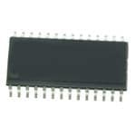
ICGOO电子元器件商城为您提供IR2130STRPBF由International Rectifier设计生产,在icgoo商城现货销售,并且可以通过原厂、代理商等渠道进行代购。 IR2130STRPBF价格参考¥72.44-¥99.15。International RectifierIR2130STRPBF封装/规格:PMIC - 栅极驱动器, Half-Bridge Gate Driver IC Inverting 28-SOIC。您可以下载IR2130STRPBF参考资料、Datasheet数据手册功能说明书,资料中有IR2130STRPBF 详细功能的应用电路图电压和使用方法及教程。
Infineon Technologies 旗下的 IR2130STRPBF 是一款高性能的栅极驱动器,属于 PMIC(电源管理集成电路)中的栅极驱动器类别。该器件集成了三相逆变器所需的全部驱动功能,适用于驱动高压、高速的 N 沟道功率 MOSFET 和 IGBT。

IR2130STRPBF 的主要应用场景包括:

1. 电机驱动:广泛用于三相交流电机、无刷直流电机(BLDC)和永磁同步电机(PMSM)的控制,常见于工业自动化、电动工具、家用电器(如洗衣机、空调压缩机)中。

2. 逆变电源系统:在不间断电源(UPS)、太阳能逆变器和电能质量调节设备中,用于高效控制功率开关器件,实现直流到交流的转换。

3. 工业控制与自动化:应用于变频器、伺服驱动器等工业控制系统,提供可靠的高边和低边驱动能力,支持高达600V的电压应用。

4. 电动车与电动交通工具:作为电机控制器的核心驱动芯片,用于电动自行车、电动滑板车及小型电动车的电驱系统。

IR2130STRPBF 内置了死区时间控制、过流保护和欠压锁定(UVLO)等安全功能,并采用 SOIC-28 封装,便于表面贴装,提升了系统可靠性与设计灵活性。其自举电路支持高边驱动,简化了电源设计,适合紧凑型高效率功率系统。
| 参数 | 数值 |
| 产品目录 | 集成电路 (IC) |
| 描述 | IC DRIVER BRIDGE 3-PHASE 28SOIC |
| 产品分类 | PMIC - MOSFET,电桥驱动器 - 外部开关 |
| 品牌 | International Rectifier |
| 数据手册 | |
| 产品图片 |
|
| 产品型号 | IR2130STRPBF |
| rohs | 无铅 / 符合限制有害物质指令(RoHS)规范要求 |
| 产品系列 | - |
| 产品培训模块 | http://www.digikey.cn/PTM/IndividualPTM.page?site=cn&lang=zhs&ptm=26250 |
| 供应商器件封装 | 28-SOIC W |
| 包装 | Digi-Reel® |
| 安装类型 | 表面贴装 |
| 封装/外壳 | 28-SOIC(0.295",7.50mm 宽) |
| 工作温度 | -40°C ~ 125°C |
| 延迟时间 | 675ns |
| 标准包装 | 1 |
| 电压-电源 | 10 V ~ 20 V |
| 电流-峰值 | 200mA |
| 输入类型 | 反相 |
| 输出数 | 3 |
| 配置 | 3 相桥 |
| 配置数 | 1 |
| 高压侧电压-最大值(自举) | 600V |


- 商务部:美国ITC正式对集成电路等产品启动337调查
- 曝三星4nm工艺存在良率问题 高通将骁龙8 Gen1或转产台积电
- 太阳诱电将投资9.5亿元在常州建新厂生产MLCC 预计2023年完工
- 英特尔发布欧洲新工厂建设计划 深化IDM 2.0 战略
- 台积电先进制程称霸业界 有大客户加持明年业绩稳了
- 达到5530亿美元!SIA预计今年全球半导体销售额将创下新高
- 英特尔拟将自动驾驶子公司Mobileye上市 估值或超500亿美元
- 三星加码芯片和SET,合并消费电子和移动部门,撤换高东真等 CEO
- 三星电子宣布重大人事变动 还合并消费电子和移动部门
- 海关总署:前11个月进口集成电路产品价值2.52万亿元 增长14.8%


PDF Datasheet 数据手册内容提取
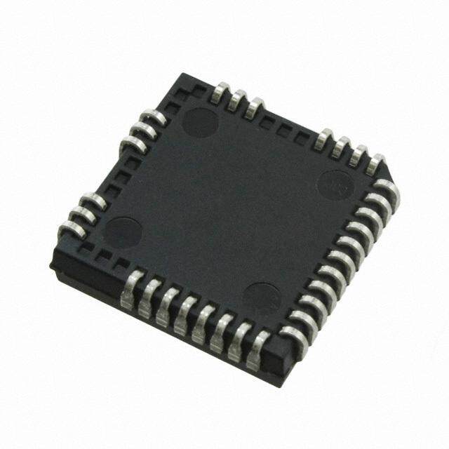
Data Sheet No. PD60019 Rev.P IR2130/IR2132(J)(S) & (PbF) 3-PHASE BRIDGE DRIVER Features Product Summary • Floating channel designed for bootstrap operation V 600V max. Fully operational to +600V OFFSET Tolerant to negative transient voltage I +/- 200 mA / 420 mA dV/dt immune O • Gate drive supply range from 10 to 20V • Undervoltage lockout for all channels VOUT 10 - 20V • Over-current shutdown turns off all six drivers • ton/off (typ.) 675 & 425 ns Independent half-bridge drivers • Matched propagation delay for all channels • Deadtime (typ.) 2.5 µs (IR2130) 2.5V logic compatible • Outputs out of phase with inputs 0.8 µs (IR2132) • Cross-conduction prevention logic • Also available LEAD-FREE Packages Description The IR2130/IR2132(J)(S) is a high voltage, high speed power MOSFET and IGBT driver with three indepen- dent high and low side referenced output channels. Pro- prietary HVIC technology enables ruggedized 28-Lead SOIC monolithic construction. Logic inputs are compatible with CMOS or LSTTL outputs, down to 2.5V logic. A 28-Lead PDIP ground-referenced operational amplifier provides analog feedback of bridge current via an external cur- rent sense resistor. A current trip function which termi- nates all six outputs is also derived from this resistor. 44-Lead PLCC w/o 12 Leads An open drain FAULT signal indicates if an over-cur- rent or undervoltage shutdown has occurred. The output drivers feature a high pulse current buffer stage designed for minimum driver cross-conduction. Propagation delays are matched to simplify use at high frequencies. The floating channels can be used to drive N-channel power MOSFETs or IGBTs in the high side configuration which operate up to 600 volts. Typical Connection (Refer to Lead Assignments for correct pin configuration). This/These diagram(s) show electrical connections only. Please refer to our Application Notes and DesignTips for proper circuit board layout. www.irf.com 1
IR2130/IR2132(J)(S) & (PbF) Absolute Maximum Ratings Absolute Maximum Ratings indicate sustained limits beyond which damage to the device may occur. All voltage param- eters are absolute voltages referenced to VS0. The Thermal Resistance and Power Dissipation ratings are measured under board mounted and still air conditions. Additional information is shown in Figures 50 through 53. Symbol Definition Min. Max. Units VB1,2,3 High Side Floating Supply Voltage -0.3 625 VS1,2,3 High Side Floating Offset Voltage VB1,2,3 - 25 VB1,2,3 + 0.3 VHO1,2,3 High Side Floating Output Voltage VS1,2,3 - 0.3 VB1,2,3 + 0.3 VCC Low Side and Logic Fixed Supply Voltage -0.3 25 VSS Logic Ground VCC - 25 VCC + 0.3 VLO1,2,3 Low Side Output Voltage -0.3 VCC + 0.3 VIN Logic Input Voltage (HIN1,2,3, LIN1,2,3 & ITRIP) VSS - 0.3 (VSS + 15) or V (VCC + 0.3) whichever is lower VFLT FAULT Output Voltage VSS - 0.3 VCC + 0.3 VCAO Operational Amplifier Output Voltage VSS - 0.3 VCC + 0.3 VCA- Operational Amplifier Inverting Input Voltage VSS - 0.3 VCC + 0.3 dVS/dt Allowable Offset Supply Voltage Transient — 50 V/ns PD Package Power Dissipation @ TA ≤ +25°C (28 Lead DIP) — 1.5 (28 Lead SOIC) — 1.6 W (44 Lead PLCC) — 2.0 RthJA Thermal Resistance, Junction to Ambient (28 Lead DIP) — 83 (28 Lead SOIC) — 78 °C/W (44 Lead PLCC) — 63 TJ Junction Temperature — 150 TS Storage Temperature -55 150 °C TL Lead Temperature (Soldering, 10 seconds) — 300 Recommended Operating Conditions The Input/Output logic timing diagram is shown in Figure 1. For proper operation the device should be used within the recommended conditions. All voltage parameters are absolute voltages referenced to VS0. The VS offset rating is tested with all supplies biased at 15V differential. Typical ratings at other bias conditions are shown in Figure 54. Symbol Definition Min. Max. Units VB1,2,3 High Side Floating Supply Voltage VS1,2,3 + 10 VS1,2,3 + 20 VS1,2,3 High Side Floating Offset Voltage Note 1 600 VHO1,2,3 High Side Floating Output Voltage VS1,2,3 VB1,2,3 VCC Low Side and Logic Fixed Supply Voltage 10 20 VSS Logic Ground -5 5 VLO1,2,3 Low Side Output Voltage 0 VCC VIN Logic Input Voltage (HIN1,2,3, LIN1,2,3 & ITRIP) VSS VSS + 5 V VFLT FAULT Output Voltage VSS VCC VCAO Operational Amplifier Output Voltage VSS VSS + 5 VCA- Operational Amplifier Inverting Input Voltage VSS VSS + 5 TA Ambient Temperature -40 125 °C Note 1: Logic operational for VS of (VS0 - 5V) to (VS0 + 600V). Logic state held for VS of (VS0 - 5V) to (VS0 - VBS). (Please refer to the Design Tip DT97-3 for more details). Note 2: All input pins, CA- and CAO pins are internally clamped with a 5.2V zener diode. 2 www.irf.com
IR2130/IR2132(J)(S) & (PbF) Dynamic Electrical Characteristics VBIAS (VCC, VBS1,2,3) = 15V, VS0,1,2,3 = VSS, CL = 1000 pF and TA = 25°C unless otherwise specified. The dynamic electrical characteristics are defined in Figures 3 through 5. Symbol Definition Figure Min. Typ. Max. Units Test Conditions ton Turn-On Propagation Delay 11 500 675 850 toff Turn-Off Propagation Delay 12 300 425 550 VIN = 0 & 5V tr Turn-On Rise Time 13 — 80 125 VS1,2,3 = 0 to 600V tf Turn-Off Fall Time 14 — 35 55 titrip ITRIP to Output Shutdown Prop. Delay 15 400 660 920 VIN, VITRIP = 0 & 5V ns tbl ITRIP Blanking Time — — 400 — VITRIP = 1V tflt ITRIP to FAULT Indication Delay 16 335 590 845 VIN, VITRIP = 0 & 5V tflt,in Input Filter Time (All Six Inputs) — — 310 — VIN = 0 & 5V tfltclr LIN1,2,3 to FAULT Clear Time 17 6.0 9.0 12.0 VIN, VITRIP = 0 & 5V DT Deadtime (IR2130) 18 1.3 2.5 3.7 µs (IR2132) 18 0.4 0.8 1.2 VIN = 0 & 5V SR+ Operational Amplifier Slew Rate (+) 19 4.4 6.2 — V/µs SR- Operational Amplifier Slew Rate (-) 20 2.4 3.2 — NOTE: For high side PWM, HIN pulse width must be ≥ 1.5µsec Static Electrical Characteristics VBIAS (VCC, VBS1,2,3) = 15V, VS0,1,2,3 = VSS and TA = 25°C unless otherwise specified. The VIN, VTH and IIN parameters are referenced to VSS and are applicable to all six logic input leads: HIN1,2,3 & LIN1,2,3. The VO and IO parameters are referenced to VS0,1,2,3 and are applicable to the respective output leads: HO1,2,3 or LO1,2,3. Symbol Definition Figure Min. Typ. Max. Units Test Conditions VIH Logic “0” Input Voltage (OUT = LO) 21 2.2 — — V VIL Logic “1” Input Voltage (OUT = HI) 22 — — 0.8 VIT,TH+ ITRIP Input Positive Going Threshold 23 400 490 580 VOH High Level Output Voltage, VBIAS - VO 24 — — 100 mV VIN = 0V, IO = 0A VOL Low Level Output Voltage, VO 25 — — 100 VIN = 5V, IO = 0A ILK Offset Supply Leakage Current 26 — — 50 µA VB = VS = 600V IQBS Quiescent VBS Supply Current 27 — 15 30 VIN = 0V or 5V IQCC Quiescent VCC Supply Current 28 — 3.0 4.0 mA VIN = 0V or 5V IIN+ Logic “1” Input Bias Current (OUT = HI) 29 — 450 650 VIN = 0V IIN- Logic “0” Input Bias Current (OUT = LO) 30 — 225 400 µA VIN = 5V IITRIP+ “High” ITRIP Bias Current 31 — 75 150 ITRIP = 5V IITRIP- “Low” ITRIP Bias Current 32 — — 100 nA ITRIP = 0V VBSUV+ VBS Supply Undervoltage Positive Going 33 7.5 8.35 9.2 Threshold VBSUV- VBS Supply Undervoltage Negative Going 34 7.1 7.95 8.8 Threshold V VCCUV+ VCC Supply Undervoltage Positive Going 35 8.3 9.0 9.7 Threshold VCCUV- VCC Supply Undervoltage Negative Going 36 8.0 8.7 9.4 Threshold Ron,FLT FAULT Low On-Resistance 37 — 55 75 Ω www.irf.com 3
IR2130/IR2132(J)(S) & (PbF) Static Electrical Characteristics -- Continued VBIAS (VCC, VBS1,2,3) = 15V, VS0,1,2,3 = VSS and TA = 25°C unless otherwise specified. The VIN, VTH and IIN parameters are referenced to VSS and are applicable to all six logic input leads: HIN1,2,3 & LIN1,2,3. The VO and IO parameters are referenced to VS0,1,2,3 and are applicable to the respective output leads: HO1,2,3 or LO1,2,3. Symbol Definition Figure Min. Typ. Max. Units Test Conditions IO+ Output High Short Circuit Pulsed Current 38 200 250 — VO = 0V, VIN = 0V PW ≤ 10 µs IO- Output Low Short Circuit Pulsed Current 39 420 500 — mA VO = 15V, VIN = 5V PW ≤ 10 µs VOS Operational Amplifer Input Offset Voltage 40 — — 30 mV VS0 = VCA- = 0.2V ICA- CA- Input Bais Current 41 — — 4.0 nA VCA- = 2.5V CMRR Op. Amp. Common Mode Rejection Ratio 42 60 80 — VS0=VCA-=0.1V & 5V PSRR Op. Amp. Power Supply Rejection Ratio 43 55 75 — dB VS0 = VCA- = 0.2V VCC = 10V & 20V VOH,AMP Op. Amp. High Level Output Voltage 44 5.0 5.2 5.4 V VCA- = 0V, VS0 = 1V VOL,AMP Op. Amp. Low Level Output Voltage 45 — — 20 mV VCA- = 1V, VS0 = 0V ISRC,AMP Op. Amp. Output Source Current 46 2.3 4.0 — VCA- = 0V, VS0 = 1V VCAO = 4V ISRC,AMP Op. Amp. Output Sink Current 47 1.0 2.1 — VCA- = 1V, VS0 = 0V mA VCAO = 2V IO+,AMP Operational Amplifier Output High Short 48 — 4.5 6.5 VCA- = 0V, VS0 = 5V Circuit Current VCAO = 0V IO-,AMP Operational Amplifier Output Low Short 49 — 3.2 5.2 VCA- = 5V, VS0 = 0V Circuit Current VCAO = 5V Lead Assignments 28 Lead PDIP 44 Lead PLCC w/o 12 Leads 28 Lead SOIC (Wide Body) IR2130 / IR2132 IR2130J / IR2132J IR2130S / IR2132S Part Number 4 www.irf.com
IR2130/IR2132(J)(S) & (PbF) Functional Block Diagram Lead Definitions Symbol Description HIN1,2,3 Logic inputs for high side gate driver outputs (HO1,2,3), out of phase LIN1,2,3 Logic inputs for low side gate driver output (LO1,2,3), out of phase FAULT Indicates over-current or undervoltage lockout (low side) has occurred, negative logic VCC Low side and logic fixed supply ITRIP Input for over-current shutdown CAO Output of current amplifier CA- Negative input of current amplifier VSS Logic ground VB1,2,3 High side floating supplies HO1,2,3 High side gate drive outputs VS1,2,3 High side floating supply returns LO1,2,3 Low side gate drive outputs VS0 Low side return and positive input of current amplifier www.irf.com 5
IR2130/IR2132(J)(S) & (PbF) HIN1,2,3 LIN1,2,3 ITRIP FAULT <50 V/ns HO1,2,3 LO1,2,3 Figure 1. Input/Output Timing Diagram Figure 2. Floating Supply Voltage Transient Test Circuit HIN1,2,3 HIN1,2,3 LIN1,2,3 50% 50% 50% 50% LIN1,2,3 ton tr toff tf LO1,2,3 90% 90% 50% 50% HO1,2,3 HO1,2,3 LO1,2,3 10% 10% DT DT Figure 3. Deadtime Waveform Definitions Figure 4. Input/Output Switching Time Waveform Definitions 6 www.irf.com
IR2130/IR2132(J)(S) & (PbF) 50% LIN1,2,3 50% ITRIP FAULT 50% 50% LO1,2,3 50% tflt tfltclr titrip Figure 5. Overcurrent Shutdown Switching Time Waveform Definitions tin,fil tin,fil U HIN/LIN on off on off on off high HO/LO low Figure 5.5 Input Filter Function V CC V + S0 CAO CA- - V SS V SS Figure 6. Diagnostic Feedback Operational Amplifier Circuit www.irf.com 7
IR2130/IR2132(J)(S) & (PbF) 15V 15V V CC 3V CA- + VS0 + VCC CAO 0V - CA- CAO V V 50 pF - S0 SS V SS + 20k ∆T1 ∆T2 0.2V 1k 3V 90% ∆V 0V 10% VCAO ∆V ∆V VOS = - 0.2V 21 SR+ = SR- = ∆T1 ∆T2 Figure 7. Operational Amplifier Slew Rate Figure 8. Operational Amplifier Input Offset Voltage Measurement Measurement V CC V 15V S0 + V CA- CAO CC - - CA- V CAO SS + VS0 V + 20k SS 0.2V 1k Measure VCAO1 at VS0 = 0.1V VCAO2 at VS0 = 5V Measure VCAO1 at VCC = 10V CMRR = -20*LOG (VCAO1-0.1V) - (VCAO2-5V) (dB) VCAO2 at VCC = 20V 4.9V VCAO1 - VCAO2 PSRR = -20*LOG (10V) (21) Figure 9. Operational Amplifier Common Mode Figure 10. Operational Amplifier Power Supply Rejection Ratio Measurements Rejection Ratio Measurements 8 www.irf.com
IR2130/IR2132(J)(S) & (PbF) 1.50 1.50 1.20 1.20 me (µs)0.90 Max. me (µs)0.90 Max. Delay Ti Typ. Delay Ti Typ. Turn-On 0.60 Min. Turn-On 0.60 Min. 0.30 0.30 0.00 0.00 -50 -25 0 25 50 75 100 125 10 12 14 16 18 20 Temperature (°C) VBIAS Supply Voltage (V) Figure 11A. Turn-On Time vs. Temperature Figure 11B. Turn-On Time vs. Supply Voltage 1.50 1.00 Max 1.20 0.80 Typ. µs) µTurn-On Time (s) 000...369000 Turn-Off Delay Time (000...246000 TMMyianpx... 0.00 0.00 0 1 2 3 4 5 6 -50 -25 0 25 50 75 100 125 Temperature (°C) Input Voltage (V) Figure 11C. Turn-On Time vs. Voltage Figure 12A. Turn-Off Time vs. Temperature 1.00 1.50 0.80 1.20 Turn-Off Delay Time (µs)00..4600 MTMyainpx... µTurn-Off Time (s) 00..6900 MTyapx 0.30 0.20 Min. 0.00 0.00 0 1 2 3 4 5 6 10 12 14 16 18 20 Input Voltage (V) VBIAS Supply Voltage (V) Figure 12C. Turn-Off Time vs. Input Voltage Figure 12B. Turn-Off Time vs. Supply Voltage www.irf.com 9
IR2130/IR2132(J)(S) & (PbF) 250 250 200 200 me (ns)150 me (ns)150 Max. On Rise Ti100 Max. On Rise Ti100 Typ. Turn- Typ. Turn- 50 50 0 0 -50 -25 0 25 50 75 100 125 10 12 14 16 18 20 Temperature (°C) VBIAS Supply Voltage (V) Figure 13A. Turn-On Rise Time vs. Temperature Figure 13B. Turn-On Rise Time vs. Voltage 125 125 100 100 Off Fall Time (ns) 5705 Off Fall Time (ns) 5705 Max. Turn- Max. Turn- Typ. Typ. 25 25 0 0 -50 -25 0 25 50 75 100 125 10 12 14 16 18 20 Temperature (°C) VBIAS Supply Voltage (V) Figure 14A. Turn-Off Fall Time vs. Temperature Figure 14B. Turn-Off Fall Time vs. Voltage 1.50 1.50 µs)1.20 µs)1.20 me ( me ( Delay Ti0.90 Max. Delay Ti0.90 Max. Output Shutdown 0.60 TMyinp.. Output Shutdown 0.60 TMyinp.. RIP to 0.30 RIP to 0.30 IT IT 0.00 0.00 -50 -25 0 25 50 75 100 125 10 12 14 16 18 20 Temperature (°C) VBIAS Supply Voltage (V) Figure 15A. ITRIP to Output Shutdown Time vs. Figure 15B. ITRIP to Output Shutdown Time vs. Voltage Temperature 10 www.irf.com
IR2130/IR2132(J)(S) & (PbF) 1.50 1.50 µs)1.20 µs)1.20 me ( me ( Delay Ti0.90 Max. Delay Ti0.90 Max. ULT Indication 0.60 Typ. ULT Indication 0.60 Typ. RIP to FA0.30 Min. RIP to FA0.30 Min. IT IT 0.00 0.00 -50 -25 0 25 50 75 100 125 10 12 14 16 18 20 Temperature (°C) VCC Supply Voltage (V) Figure 16A. ITRIP to FAULT Indication Time vs. Figure 16B. ITRIP to FAULT Indication Time vs. Voltage Temperature 25.0 25.0 20.0 20.0 me (µs) me (µs) LIN1,2,3 to FAULT Clear Ti11055...000 TMMyianpx... LIN1,2,3 to FAULT Clear Ti11055...000 MTMyainpx... 0.0 0.0 -50 -25 0 25 50 75 100 125 10 12 14 16 18 20 Temperature (°C) VCC Supply Voltage (V) Figure 17A. LIN1,2,3 to FAULT Clear Time vs. Figure 17B. LIN1,2,3 to FAULT Clear Time vs. Voltage Temperature 7.50 7.50 6.00 6.00 me (µs)4.50 Max. me (µs)4.50 Max. Deadti3.00 Typ. Deadti3.00 Typ. 1.50 Min. 1.50 Min. 0.00 0.00 -50 -25 0 25 50 75 100 125 10 12 14 16 18 20 Temperature (°C) VBIAS Supply Voltage (V) Figure 18A. Deadtime vs. Temperature (IR2130) Figure 18B. Deadtime vs. Voltage (IR2130) www.irf.com 11
IR2130/IR2132(J)(S) & (PbF) 2.50 2.50 2.00 2.00 µs)1.50 Max. µs)1.50 me ( me ( Max. Deadti1.00 Typ. Deadti1.00 Typ. 0.50 Min. 0.50 Min. 0.00 0.00 -50 -25 0 25 50 75 100 125 10 12 14 16 18 20 Temperature (°C) VBIAS Supply Voltage (V) Figure 18C. Deadtime vs. Temperature (IR2132) Figure 18D. Deadtime vs. Voltage (IR2132) 10.0 10.0 8.0 8.0 µs) Typ. µs) mplifier Slew Rate + (V/ 46..00 Min. mplifier Slew Rate + (V/ 46..00 MTyinp.. A A 2.0 2.0 0.0 0.0 -50 -25 0 25 50 75 100 125 10 12 14 16 18 20 Temperature (°C) VCC Supply Voltage (V) Figure 19A. Amplifier Slew Rate (+) vs. Temperature Figure 19B. Amplifier Slew Rate (+) vs. Voltage 5.00 5.00 4.00 4.00 mplifier Slew Rate - (V/µs)23..0000 TMyinp.. mplifier Slew Rate - (V/µs)23..0000 MTyinp.. A A 1.00 1.00 0.00 0.00 -50 -25 0 25 50 75 100 125 10 12 14 16 18 20 Temperature (°C) VCC Supply Voltage (V) Figure 20A. Amplifier Slew Rate (-) vs. Temperature Figure 20B. Amplifier Slew Rate (-) vs. Voltage 12 www.irf.com
IR2130/IR2132(J)(S) & (PbF) 5.00 5.00 4.00 4.00 Logic "0" Input Threshold (V)23..0000 Min. Logic "0" Input Threshold (V)23..0000 Min. 1.00 1.00 0.00 0.00 -50 -25 0 25 50 75 100 125 10 12 14 16 18 20 Temperature (°C) VCC Supply Voltage (V) Figure 21A. Logic “0” Input Threshold vs. Temperature Figure 20B. Logic “0” Input Threshold vs. Voltage 5.00 5.00 4.00 4.00 Logic "1" Input Threshold (V)23..0000 Logic "1" Input Threshold (V)23..0000 1.00 Max. 1.00 Max. 0.00 0.00 -50 -25 0 25 50 75 100 125 10 12 14 16 18 20 Temperature (°C) VCC Supply Voltage (V) Figure 22A. Logic “1” Input Threshold vs. Temperature Figure 22B. Logic “1” Input Threshold vs. Voltage 750 750 mV)600 Max. mV)600 Max. Going Threshold (450 TMyinp.. Going Threshold (450 TMyinp.. ITRIP Input Positive 135000 ITRIP Input Positive 135000 0 0 -50 -25 0 25 50 75 100 125 10 12 14 16 18 20 Temperature (°C) VCC Supply Voltage (V) Figure 23A. ITRIP Input Positive Going Threshold Figure 23B. ITRIP Input Positive Going Threshold vs. Temperature vs. Voltage www.irf.com 13
IR2130/IR2132(J)(S) & (PbF) 1.00 1.00 0.80 0.80 Output Voltage (V)0.60 Output Voltage (V)0.60 High Level 0.40 High Level 0.40 0.20 0.20 Max. Max. 0.00 0.00 -50 -25 0 25 50 75 100 125 10 12 14 16 18 20 Temperature (°C) VBIAS Supply Voltage (V) Figure 24A. High Level Output vs. Temperature Figure 24B. High Level Output vs. Voltage 1.00 1.00 0.80 0.80 Output Voltage (V)0.60 Output Voltage (V)0.60 w Level 0.40 w Level 0.40 Lo Lo 0.20 0.20 Max. Max. 0.00 0.00 -50 -25 0 25 50 75 100 125 10 12 14 16 18 20 Temperature (°C) VBIAS Supply Voltage (V) Figure 25A. Low Level Output vs. Temperature Figure 25B. Low Level Output vs. Voltage 500 500 400 400 Offset Supply Leakage Current (µA)123000000 Offset Supply Leakage Current (µA)123000000 Max. Max. 0 0 -50 -25 0 25 50 75 100 125 0 100 200 300 400 500 600 Temperature (°C) VB Boost Voltage (V) Figure 26A. Offset Supply Leakage Current Figure 26B. Offset Supply Leakage Current vs. Voltage vs. Temperature 14 www.irf.com
IR2130/IR2132(J)(S) & (PbF) 100 100 80 80 µA) µA) Current ( 60 Current ( 60 V Supply BS 40 V Supply BS 40 Max. 20 20 Max. Typ. Typ. 0 0 -50 -25 0 25 50 75 100 125 10 12 14 16 18 20 Temperature (°C) VBS Floating Supply Voltage (V) Figure 27A. VBS Supply Current vs. Temperature Figure 27B. VBS Supply Current vs. Voltage 10.0 10.0 8.0 8.0 mA) mA) V Supply Current (CC 46..00 Max. V Supply Current (CC 46..00 Max. 2.0 Typ. 2.0 Typ. 0.0 0.0 -50 -25 0 25 50 75 100 125 10 12 14 16 18 20 Temperature (°C) VCC Supply Voltage (V) Figure 28A. VCC Supply Current vs. Temperature Figure 28B. VCC Supply Current vs. Voltage 1.25 1.25 1.00 1.00 mA) mA) Current (0.75 Current (0.75 Logic "1" Input Bias 00..2550 MTyapx.. Logic "1" Input Bias 00..2550 MTyapx.. 0.00 0.00 -50 -25 0 25 50 75 100 125 10 12 14 16 18 20 Temperature (°C) VCC Supply Voltage (V) Figure 29A. Logic “1” Input Current vs. Temperature Figure 29A. Logic “1” Input Current vs. Voltage www.irf.com 15
IR2130/IR2132(J)(S) & (PbF) 1.25 1.25 1.00 1.00 mA) mA) Current (0.75 Current (0.75 Logic "0" Input Bias 00..2550 Max. Logic "0" Input Bias 00..2550 Max. Typ. Typ. 0.00 0.00 -50 -25 0 25 50 75 100 125 10 12 14 16 18 20 Temperature (°C) VCC Supply Voltage (V) Figure 30A. Logic “0” Input Current vs. Temperature Figure 30B. Logic “0” Input Current vs. Voltage 500 500 400 400 "High" ITRIP Bias Current (µA)123000000 TMyapx.. "High" ITRIP Bias Current (µA)123000000 MTyapx.. 0 0 -50 -25 0 25 50 75 100 125 10 12 14 16 18 20 Temperature (°C) VCC Supply Voltage (V) Figure 31A. “High” ITRIP Current vs. Temperature Figure 31B. “High” ITRIP Current vs. Voltage 250 500 200 400 "Low" ITRIP Bias Current (nA)110500 Max. "Low" ITRIP Bias Current (µA)230000 Max. 50 100 0 0 -50 -25 0 25 50 75 100 125 10 12 14 16 18 20 Temperature (°C) VCC Supply Voltage (V) Figure 32A. “Low” ITRIP Current vs. Temperature Figure 32B. “Low” ITRIP Current vs. Voltage 16 www.irf.com
IR2130/IR2132(J)(S) & (PbF) 11.0 11.0 10.0 10.0 V Undervoltage Lockout + (V)BS 789...000 TMMyianpx... V Undervoltage Lockout - (V)BS 789...000 TMMyianpx... 6.0 6.0 -50 -25 0 25 50 75 100 125 -50 -25 0 25 50 75 100 125 Temperature (°C) Temperature (°C) Figure 33. VBS Undervoltage (+) vs. Temperature Figure 34. VBS Undervoltage (-) vs. Temperature 11.0 11.0 10.0 10.0 Max. V Undervoltage Lockout + (V)CC 89..00 TMyinp.. V Undervoltage Lockout - (V)CC 89..00 TMMyianpx... 7.0 7.0 6.0 6.0 -50 -25 0 25 50 75 100 125 -50 -25 0 25 50 75 100 125 Temperature (°C) Temperature (°C) Figure 35. VCC Undervoltage (+) vs. Temperature Figure 36. VCC Undervoltage (-) vs. Temperature 250 250 200 200 ms) ms) Resistance (oh150 Resistance (oh150 w On 100 w On 100 Max. FAULT- Lo 50 Max. FAULT- Lo 50 Typ. Typ. 0 0 -50 -25 0 25 50 75 100 125 10 12 14 16 18 20 Temperature (°C) VCC Supply Voltage (V) Figure 37A. FAULT Low On Resistance vs. Figure 37B. FAULT Low On Resistance vs. Voltage Temperature www.irf.com 17
IR2130/IR2132(J)(S) & (PbF) 500 500 400 400 mA) mA) Output Source Current (230000 MTyinp.. Output Source Current (230000 Typ. 100 100 Min. 0 0 -50 -25 0 25 50 75 100 125 10 12 14 16 18 20 Temperature (°C) VBIAS Supply Voltage (V) Figure 38A. Output Source Current vs. Temperature Figure 38B. Output Source Current vs. Voltage 750 750 625 600 Typ. mA) Min. mA)500 Output Sink Current (340500 Output Sink Current (235705 MTyinp.. 150 125 0 0 -50 -25 0 25 50 75 100 125 10 12 14 16 18 20 Temperature (°C) VBIAS Supply Voltage (V) Figure 39A. Output Sink Current vs. Temperature Figure 39B. Output Sink Current vs. Voltage 50 50 40 40 mV) mV) Offset Voltage (30 Max. Offset Voltage (30 Max. mplifier Input 20 mplifier Input 20 A10 A10 0 0 -50 -25 0 25 50 75 100 125 10 12 14 16 18 20 Temperature (°C) VCC Supply Voltage (V) Figure 40A. Amplifier Input Offset vs. Temperature Figure 40B. Amplifier Input Offset vs. Voltage 18 www.irf.com
IR2130/IR2132(J)(S) & (PbF) 10.0 10.0 8.0 8.0 Current (nA) 6.0 Current (nA) 6.0 CA- Input Bias 4.0 Max. CA- Input Bias 4.0 Max. 2.0 2.0 0.0 0.0 -50 -25 0 25 50 75 100 125 10 12 14 16 18 20 Temperature (°C) VCC Supply Voltage (V) Figure 41A. CA- Input Current vs. Temperature Figure 41B. CA- Input Current vs. Voltage 100 100 Typ. 80 Typ. 80 R (dB) 60 Min. R (dB) 60 Min. R R M M C C mplifier 40 mplifier 40 A A 20 20 0 0 -50 -25 0 25 50 75 100 125 10 12 14 16 18 20 Temperature (°C) VCC Supply Voltage (V) Figure 42A. Amplifier CMRR vs. Temperature Figure 42B. Amplifier CMRR vs. Voltage 100 100 80 80 Typ. Typ. mplifier PSRR (dB) 4600 Min. mplifier PSRR (dB) 4600 Min. A A 20 20 0 0 -50 -25 0 25 50 75 100 125 10 12 14 16 18 20 Temperature (°C) VCC Supply Voltage (V) Figure 43A. Amplifier PSRR vs. Temperature Figure 43B. Amplifier PSRR vs. Voltage www.irf.com 19
IR2130/IR2132(J)(S) & (PbF) 6.00 6.00 Output Voltage (V)55..4700 Max. Output Voltage (V)55..4700 Max. High Level 5.10 TMyinp.. High Level 5.10 TMyinp.. mplifier 4.80 mplifier 4.80 A A 4.50 4.50 -50 -25 0 25 50 75 100 125 10 12 14 16 18 20 Temperature (°C) VCC Supply Voltage (V) Figure 44A. Amplifier High Level Output vs. Figure 44B. Amplifier High Level Output vs. Voltage Temperature 100 100 mV) 80 mV) 80 Output Voltage ( 60 Output Voltage ( 60 w Level 40 w Level 40 mplifier Lo 20 Max. mplifier Lo 20 Max. A A 0 0 -50 -25 0 25 50 75 100 125 10 12 14 16 18 20 Temperature (°C) VCC Supply Voltage (V) Figure 45A. Amplifier Low Level Output vs. Figure 45B. Amplifier Low Level Output vs. Voltage Temperature 10.0 10.0 Amplifier Output Source Current (mA) 2468....0000 TMyinp.. Amplifier Output Source Current (mA) 2468....0000 Typ. Min. 0.0 0.0 -50 -25 0 25 50 75 100 125 10 12 14 16 18 20 Temperature (°C) VCC Supply Voltage (V) Figure 46A. Amplifier Output Source Current vs. Figure 46B. Amplifier Output Source Current vs. Temperature Voltage 20 www.irf.com
IR2130/IR2132(J)(S) & (PbF) 5.00 5.00 4.00 4.00 mA) mA) Output Sink Current (23..0000 Typ. Output Sink Current (23..0000 Amplifier 1.00 Min. Amplifier 1.00 TMyinp.. 0.00 0.00 -50 -25 0 25 50 75 100 125 10 12 14 16 18 20 Temperature (°C) VCC Supply Voltage (V) Figure 47A. Amplifier Output Sink Current vs. Figure 47B. Amplifier Output Sink Current vs. Voltage Temperature 15.0 15.0 mA)12.0 mA)12.0 Current ( 9.0 Current ( 9.0 Circuit Max. Circuit High Short 6.0 Typ. High Short 6.0 Output 3.0 Output 3.0 Max. Typ. 0.0 0.0 -50 -25 0 25 50 75 100 125 10 12 14 16 18 20 Temperature (°C) VCC Supply Voltage (V) Figure 48A. Amplifier Output High Short Circuit Figure 48B. Amplifier Output High Short Circuit Current vs. Temperature Current vs. Voltage 15.0 15.0 mA)12.0 mA)12.0 Current ( 9.0 Current ( 9.0 Circuit Circuit w Short 6.0 Max. w Short 6.0 Output Lo 3.0 Typ. Output Lo 3.0 Max. Typ. 0.0 0.0 -50 -25 0 25 50 75 100 125 10 12 14 16 18 20 Temperature (°C) VCC Supply Voltage (V) Figure 49A. Amplifier Output Low Short Circuit Current Figure 49B. Amplifier Output Low Short Circuit Current vs. Temperature vs. Voltage www.irf.com 21
IR2130/IR2132(J)(S) & (PbF) 0.0 -3.0 Offset Supply Voltage (V) --96..00 Typ. V S -12.0 -15.0 10 12 14 16 18 20 VBS Floating Supply Voltage (V) Figure 50. Maximum VS Negative Offset vs. VBS Supply Voltage 50 50 480V 480V 45 45 Junction Temperature (°C)334050 31026V00VV Junction Temperature (°C)334050 31026V00VV 25 25 20 20 1E+2 1E+3 1E+4 1E+5 1E+2 1E+3 1E+4 1E+5 Frequency (Hz) Frequency (Hz) Figure 51. IR2130/IR2132 TJ vs. Frequency (IRF820) Figure 52. IR2130/IR2132 TJ vs. Frequency (IRF830) RGATE = 33ΩΩΩΩΩ, VCC = 15V RGATE = 20ΩΩΩΩΩ, VCC = 15V 100 140 480V 120 80 320V Junction Temperature (°C) 4600 342800VV Junction Temperature (°C)1068000 106V0V 160V 40 0V 20 20 1E+2 1E+3 1E+4 1E+5 1E+2 1E+3 1E+4 1E+5 Frequency (Hz) Frequency (Hz) Figure 53. IR2130/IR2132 TJ vs. Frequency (IRF840) Figure 54. IR2130/IR2132 TJ vs. Frequency (IRF450) RGATE = 15ΩΩΩΩΩ, VCC = 15V RGATE = 10ΩΩΩΩΩ, VCC = 15V 22 www.irf.com
IR2130/IR2132(J)(S) & (PbF) 120 120 110 110 100 100 ) ) Junction Temperature (°C 34567890000000 413862000VVV Junction Temperature (°C 34567890000000 413862000VV 20 0V 20 0V 1E+2 1E+3 1E+4 1E+5 1E+2 1E+3 1E+4 1E+5 Frequency (Hz) Frequency (Hz) Figure 55. IR2130J/IR2132J Figure 56. IR2130J/IR2132J TJ vs. Frequency (IRGPC20KD2) TJ vs. Frequency (IRGPC30KD2) RGATE = 33ΩΩΩΩΩ, VCC = 15V RGATE = 20ΩΩΩΩΩ, VCC = 15V 120 120 480V 110 110 100 100 ) erature (°C) 789000 perature (°C 789000 136200VV p 60 480V m 60 m e Junction Te 345000 31026V00VV Junction T 345000 0V 20 20 1E+2 1E+3 1E+4 1E+5 1E+2 1E+3 1E+4 1E+5 Frequency (Hz) Frequency (Hz) Figure 57. IR2130J/IR2132J Figure 58. IR2130J/IR2132J TJ vs. Frequency (IRGPC40KD2) TJ vs. Frequency (IRGPC50KD2) RGATE = 15ΩΩΩΩΩ, VCC = 15V RGATE = 10ΩΩΩΩΩ, VCC = 15V www.irf.com 23
IR2130/IR2132(J)(S) & (PbF) Case outlines 28-Lead PDIP (wide body) 01-6011 01-3024 02 (MS-011AB) 01-6013 28-Lead SOIC (wide body) 01-304002 (MS-013AE) 24 www.irf.com
IR2130/IR2132(J)(S) & (PbF) Case outline NOTES 01-6009 00 44-Lead PLCC w/o 12 leads 01-3004 02(mod.) (MS-018AC) www.irf.com 25
IR2130/IR2132(J)(S) & (PbF) LEADFREE PART MARKING INFORMATION IRxxxxxx Part number YWW? Date code IR logo ?XXXX Pin 1 Identifier Lot Code ? MARKING CODE (Prod mode - 4 digit SPN code) P Lead Free Released Non-Lead Free Released Assembly site code Per SCOP 200-002 ORDER INFORMATION Basic Part (Non-Lead Free) Leadfree Part 28-Lead PDIP IR2130 order IR2130 28-Lead PDIP IR2130 order IR2130PbF 28-Lead SOIC IR2130S order IR2130S 28-Lead SOIC IR2130S order IR2130SPbF 28-Lead PDIP IR2132 order IR2132 28-Lead PDIP IR2132 order IR2132PbF 28-Lead SOIC IR2132S order IR2132S 28-Lead SOIC IR2132S order IR2132SPbF 44-Lead PLCC IR2130J order IR2130J 44-Lead PLCC IR2130J order IR2130JPbF 44-Lead PLCC IR2132J order IR2132J 44-Lead PLCC IR2132J order IR2132JPbF IR WORLD HEADQUARTERS: 233 Kansas St., El Segundo, California 90245 Tel: (310) 252-7105 This product has been qualified per industrial level Data and specifications subject to change without notice. 4/2/2004 26 www.irf.com
Mouser Electronics Authorized Distributor Click to View Pricing, Inventory, Delivery & Lifecycle Information: I nfineon: IR2130JPbF IR2130PbF IR2130SPbF IR2132JPbF IR2132PbF IR2132SPbF IR2130JTRPBF IR2130STRPBF IR2132STRPBF IR2132JTRPBF