ICGOO在线商城 > 隔离器 > 光隔离器 - 晶体管,光电输出 > IL300-X016
 Datasheet下载
- 型号: IL300-X016
- 制造商: Vishay
- 库位|库存: xxxx|xxxx
- 要求:
| 数量阶梯 | 香港交货 | 国内含税 |
| +xxxx | $xxxx | ¥xxxx |
查看当月历史价格
查看今年历史价格
IL300-X016产品简介:
ICGOO电子元器件商城为您提供IL300-X016由Vishay设计生产,在icgoo商城现货销售,并且可以通过原厂、代理商等渠道进行代购。 IL300-X016价格参考。VishayIL300-X016封装/规格:光隔离器 - 晶体管,光电输出, 光隔离器 光伏,线性化 输出 5300Vrms 1 通道 8-DIP。您可以下载IL300-X016参考资料、Datasheet数据手册功能说明书,资料中有IL300-X016 详细功能的应用电路图电压和使用方法及教程。
IL300-X016 是 Vishay Semiconductor Opto Division 生产的一款光隔离器(光电耦合器),属于晶体管输出型光耦。它具有高线性度和良好的隔离性能,常用于需要电气隔离和信号传输的场合。

应用场景包括:

1. 电源管理系统:用于隔离反馈信号,确保主控电路与高压侧电路之间的安全隔离,如开关电源、DC-DC转换器等。

2. 工业控制设备:在PLC(可编程逻辑控制器)、工业自动化系统中,用于隔离输入输出信号,提高系统抗干扰能力与安全性。

3. 电机驱动与变频器:用于隔离控制信号与功率部分,防止高压干扰或损坏控制电路。

4. 医疗电子设备:在需要符合严格安全标准的医疗设备中,实现信号隔离,保障患者和设备安全。

5. 测量与检测仪器:用于隔离模拟或数字信号,在高精度测量系统中保持信号完整性。

6. 通信设备:在通信接口电路中实现电平转换与隔离,防止地环路干扰。

该器件具有单通道、高速响应和高稳定性的特点,适用于对信号传输精度和系统安全性有较高要求的应用场合。
| 参数 | 数值 |
| 产品目录 | |
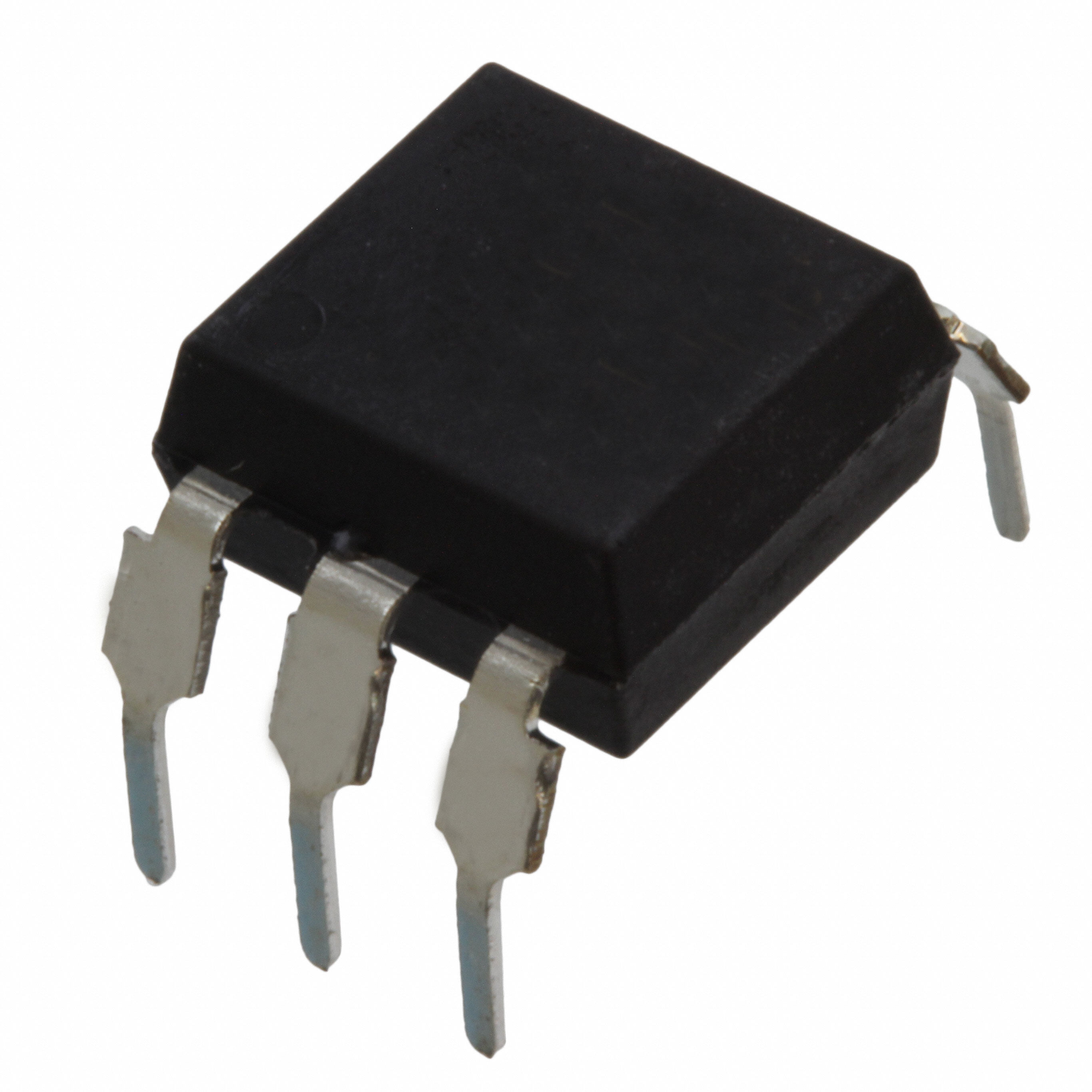
| 描述 | OPTOISO 5.3KV PHVOLT 8DIP高线性光耦合器 Single Linear, High Gain, Wide Bandwidth |
| 产品分类 | |
| 品牌 | Vishay SemiconductorsVishay Semiconductor Opto Division |
| 产品手册 | |
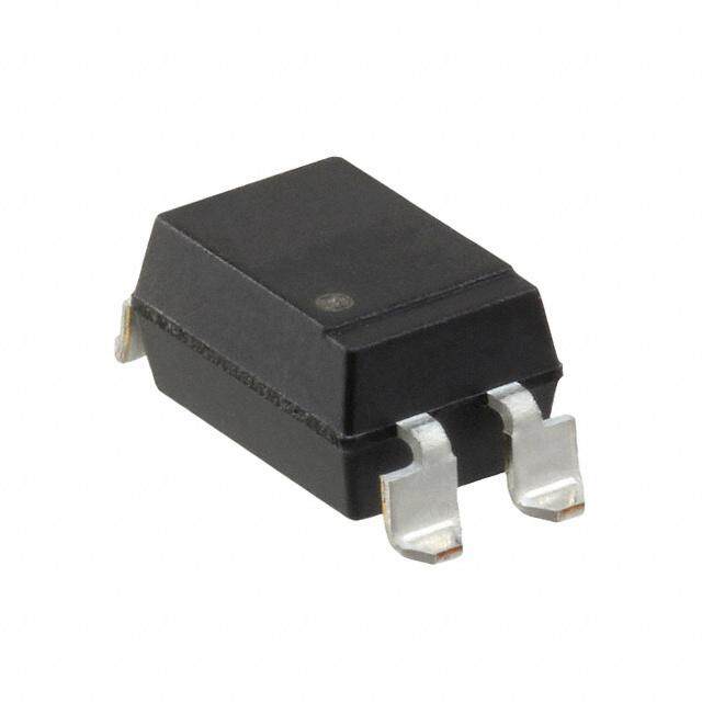
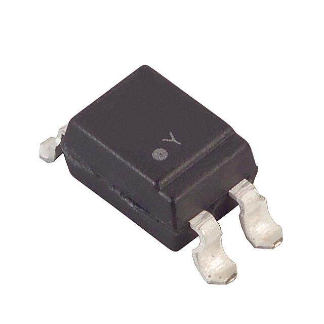
| 产品图片 | |
| rohs | 符合RoHS无铅 / 符合限制有害物质指令(RoHS)规范要求 |
| 产品系列 | 光耦合器/光电耦合器,高线性光耦合器,Vishay Semiconductors IL300-X016- |
| 数据手册 | |
| 产品型号 | IL300-X016IL300-X016 |
| Vce饱和值(最大值) | - |
| 上升/下降时间(典型值) | 1µs, 1µs |
| 产品种类 | 高线性光耦合器 |
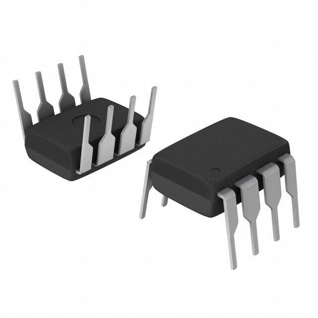
| 供应商器件封装 | 8-DIP |
| 包装 | 带卷 (TR) |
| 商标 | Vishay Semiconductors |
| 安装类型 | 通孔 |
| 封装 | Tube |
| 封装/外壳 | 8-DIP(0.400",10.16mm) |
| 封装/箱体 | DIP-8 |
| 工作温度 | -55°C ~ 100°C |
| 工厂包装数量 | 2000 |
| 打开/关闭时间(典型值) | - |
| 最大上升时间 | 1.75 us |
| 最大下降时间 | 1.75 us |
| 最大功率耗散 | 210 mW |
| 最大反向二极管电压 | 5 V |
| 最大工作温度 | + 100 C |
| 最大正向二极管电压 | 1.5 V |
| 最大输入二极管电流 | 60 mA |
| 最小工作温度 | - 55 C |
| 标准包装 | 2,000 |
| 正向电压 | 1.25 V |
| 正向电流 | 10 mA |
| 每芯片的通道数量 | 1 Channel |
| 电压-正向(Vf)(典型值) | 1.25V |
| 电压-输出(最大值) | 500mV |
| 电压-隔离 | 5300Vrms |
| 电流-DC正向(If) | 60mA |
| 电流-输出/通道 | - |
| 电流传输比(最大值) | - |
| 电流传输比(最小值) | - |
| 电流传递比 | 0.5 % to 1.1 % |
| 绝缘电压 | 5300 Vrms |
| 输入类型 | DCAC/DC |
| 输出类型 | DCPhotovoltaic, Linearized |
| 输出设备 | PIN Photodiode |
| 通道数 | 1 |
| 配置 | 1 Channel |

.jpg)
.jpg)
.jpg)

- 商务部:美国ITC正式对集成电路等产品启动337调查
- 曝三星4nm工艺存在良率问题 高通将骁龙8 Gen1或转产台积电
- 太阳诱电将投资9.5亿元在常州建新厂生产MLCC 预计2023年完工
- 英特尔发布欧洲新工厂建设计划 深化IDM 2.0 战略
- 台积电先进制程称霸业界 有大客户加持明年业绩稳了
- 达到5530亿美元!SIA预计今年全球半导体销售额将创下新高
- 英特尔拟将自动驾驶子公司Mobileye上市 估值或超500亿美元
- 三星加码芯片和SET,合并消费电子和移动部门,撤换高东真等 CEO
- 三星电子宣布重大人事变动 还合并消费电子和移动部门
- 海关总署:前11个月进口集成电路产品价值2.52万亿元 增长14.8%

PDF Datasheet 数据手册内容提取
IL300 www.vishay.com Vishay Semiconductors Linear Optocoupler, High Gain Stability, Wide Bandwidth FEATURES • Couples AC and DC signals • 0.01 % servo linearity C 1 8 NC • Wide bandwidth, > 200 kHz A 2 7 NC • High gain stability, ± 0.005 %/°C typically K1 K2 C 3 6 C • Low input-output capacitance • Low power consumption, < 15 mW A 4 5 A • Isolation rated voltage 4420 V i179026_2 RMS • Internal insulation distance, > 0.4 mm DVE • Material categorization: for definitions of compliance please see www.vishay.com/doc?99912 APPLICATIONS DESCRIPTION • Power supply feedback voltage / current • Medical sensor isolation The IL300 linear optocoupler consists of an AlGaAs IRLED irradiating an isolated feedback and an output PIN • Audio signal interfacing photodiode in a bifurcated arrangement. The feedback • Isolated process control transducers photodiode captures a percentage of the LEDs flux and • Digital telephone isolation generates a control signal (I ) that can be used to servo the P1 LED drive current. This technique compensates for the AGENCY APPROVALS LED’s non-linear, time, and temperature characteristics. • UL The output PIN photodiode produces an output signal (I ) P2 that is linearly related to the servo optical flux created by the • cUL LED. • DIN EN 60747-5-5 (VDE 0884-5) available with option 1 The time and temperature stability of the input-output • BSI coupler gain (K3) is insured by using matched PIN • FIMKO photodiodes that accurately track the output flux of the LED. • CQC ORDERING INFORMATION DIP-8 O p t i o n 6 I L 3 0 0 - D E F G - X 0 # # T PART NUMBER K3 BIN PACKAGE OPTION TAPE 7.62 mm 10.16 mm AND Option 7 Option 9 REEL > 0.7 mm > 0.1 mm AGENCY CERTIFIED / K3 BIN PACKAGE UL, cUL, 0.557 to 1.618 0.765 to 1.181 0.851 to 1.181 0.765 to 0.955 0.851 to 1.061 0.945 to 1.181 0.851 to 0.955 0.945 to 1.061 BSI, FIMKO DIP-8 IL300 IL300-DEFG - - IL300-EF - IL300-E IL300-F DIP-8, 400 mil, IL300-X006 IL300-DEFG-X006 - - IL300-EF-X006 IL300-FG-X006 IL300-E-X006 IL300-F-X006 option 6 SMD-8, option 7IL300-X007T(1)IL300-DEFG-X007T(1)IL300-EFG-X007IL300-DE-X007TIL300-EF-X007T(1)IL300-FG-X007TIL300-E-X007TIL300-F-X007T(1) SMD-8, option 9IL300-X009T(1)IL300-DEFG-X009T(1) - - IL300-EF-X009T(1) - - IL300-F-X009T(1) VDE, UL, 0.557 to 1.618 0.765 to 1.181 0.851 to 1.181 0.765 to 0.955 0.851 to 1.061 0.945 to 1.181 0.851 to 0.955 0.945 to 1.061 BSI, FIMKO DIP-8 IL300-X001 IL300-DEFG-X001 - - IL300-EF-X001 - IL300-E-X001 IL300-F-X001 DIP-8, 400 mil, IL300-X016 IL300-DEFG-X016 IL300-EFG-X016 - IL300-EF-X016 - - IL300-F-X016 option 6 SMD-8, option 7 IL300-X017 IL300-DEFG-X017T(1) - - IL300-EF-X017T(1) - IL300-E-X017TIL300-F-X017T(1) SMD-8, option 9 - - - - - - IL300-E-X009TIL300-F-X019T(1) Note (1) Also available in tubes, do not put “T” on the end Rev. 2.0, 05-Mar-18 1 Document Number: 83622 For technical questions, contact: optocoupleranswers@vishay.com THIS DOCUMENT IS SUBJECT TO CHANGE WITHOUT NOTICE. THE PRODUCTS DESCRIBED HEREIN AND THIS DOCUMENT ARE SUBJECT TO SPECIFIC DISCLAIMERS, SET FORTH AT www.vishay.com/doc?91000
IL300 www.vishay.com Vishay Semiconductors ABSOLUTE MAXIMUM RATINGS (T = 25 °C, unless otherwise specified) amb PARAMETER TEST CONDITION SYMBOL VALUE UNIT INPUT Power dissipation P 160 mW diss Derate linearly from 25 °C 2.13 mW/°C Forward current I 60 mA F Surge current (pulse width < 10 μs) I 250 mA PK Reverse voltage V 5 V R Thermal resistance R 470 K/W th Junction temperature T 100 °C j OUTPUT Power dissipation P 50 mW diss Derate linearly from 25 °C 0.65 mW/°C Reverse voltage V 50 V R Thermal resistance R 1500 K/W th Junction temperature T 100 °C j COUPLER Total package dissipation at 25 °C P 210 mW tot Derate linearly from 25 °C 2.8 mW/°C Storage temperature T -55 to +150 °C stg Operating temperature T -55 to +100 °C amb Note • Stresses in excess of the absolute maximum ratings can cause permanent damage to the device. Functional operation of the device is not implied at these or any other conditions in excess of those given in the operational sections of this document. Exposure to absolute maximum ratings for extended periods of the time can adversely affect reliability ELECTRICAL CHARACTERISTICS (T = 25 °C, unless otherwise specified) amb PARAMETER TEST CONDITION SYMBOL MIN. TYP. MAX. UNIT INPUT (LED EMITTER) Forward voltage I = 10 mA V - 1.25 1.50 V F F V temperature coefficient ΔV /Δ°C - -2.2 - mV/°C F F Reverse current V = 5 V I - 1 - μA R R Junction capacitance V = 0 V, f = 1 MHz C - 15 - pF F j Dynamic resistance I = 10 mA ΔV /ΔI - 6 - Ω F F F OUTPUT Dark current V = -15 V, I = 0 A I - 1 25 nA det F D Open circuit voltage I = 10 mA V - 500 - mV F D Short circuit current I = 10 mA I - 120 - μA F SC Junction capacitance V = 0 V, f = 1 MHz C - 12 - pF F j Noise equivalent power V = 15 V NEP - 4 x 10-14 - W/√Hz det COUPLER Input-output capacitance V = 0 V, f = 1 MHz - 1 - pF F K1, servo gain (I /I ) I = 10 mA, V = -15 V K1 0.006 0.012 0.017 P1 F F det Servo photocurrent (1)(2) I = 10 mA, V = -15 V I - 120 - μA F det P1 K2, forward gain (I /I ) I = 10 mA, V = -15 V K2 0.006 0.012 0.017 P2 F F det Forward current I = 10 mA, V = -15 V I - 120 - μA F det P2 K3, transfer gain (K2/K1) (1)(2) I = 10 mA, V = -15 V K3 0.56 1 1.65 K2/K1 F det Transfer gain stability I = 10 mA, V = -15 V ΔK3/ΔT - ± 0.005 ± 0.15 %/°C F det A I = 1 mA to 10 mA ΔK3 - ± 0.25 - % F Transfer gain linearity I = 1 mA to 10 mA, T = 0 °C to 75 °C - ± 0.5 - % F amb Rev. 2.0, 05-Mar-18 2 Document Number: 83622 For technical questions, contact: optocoupleranswers@vishay.com THIS DOCUMENT IS SUBJECT TO CHANGE WITHOUT NOTICE. THE PRODUCTS DESCRIBED HEREIN AND THIS DOCUMENT ARE SUBJECT TO SPECIFIC DISCLAIMERS, SET FORTH AT www.vishay.com/doc?91000
IL300 www.vishay.com Vishay Semiconductors ELECTRICAL CHARACTERISTICS (T = 25 °C, unless otherwise specified) amb PARAMETER TEST CONDITION SYMBOL MIN. TYP. MAX. UNIT PHOTOCONDUCTIVE OPERATION Frequency response I = 10 mA, MOD = ± 4 mA, R = 50 Ω BW (-3 db) - 200 - kHz Fq L Phase response at 200 kHz V = -15 V - -45 - Deg. det Notes • Minimum and maximum values were tested requirements. Typical values are characteristics of the device and are the result of engineering evaluation. Typical values are for information only and are not part of the testing requirements (1) Bin sorting: K3 (transfer gain) is sorted into bins that are ± 6 %, as follows: Bin A = 0.557 to 0.626 Bin B = 0.620 to 0.696 Bin C = 0.690 to 0.773 Bin D = 0.765 to 0.859 Bin E = 0.851 to 0.955 Bin F = 0.945 to 1.061 Bin G = 1.051 to 1.181 Bin H = 1.169 to 1.311 Bin I = 1.297 to 1.456 Bin J = 1.442 to 1.618 K3 = K2/K1. K3 is tested at I = 10 mA, V = -15 V F det (2) Bin categories: All IL300s are sorted into a K3 bin, indicated by an alpha character that is marked on the part. The bins range from “A” through “J”. The IL300 is shipped in tubes of 50 each. Each tube contains only one category of K3. The category of the parts in the tube is marked on the tube label as well as on each individual part (3) Category options: standard IL300 orders will be shipped from the categories that are available at the time of the order. Any of the ten categories may be shipped. For customers requiring a narrower selection of bins, the bins can be grouped together as follows: IL300-DEFG: order this part number to receive categories D, E, F, G only IL300-EF: order this part number to receive categories E, F only IL300-E: order this part number to receive category E only SWITCHING CHARACTERISTICS PARAMETER TEST CONDITION SYMBOL MIN. TYP. MAX. UNIT t - 1 - μs Switching time ΔI = 2 mA, I = 10 mA r F Fq t - 1 - μs f Rise time t - 1.75 - μs r Fall time t - 1.75 - μs f COMMON MODE TRANSIENT IMMUNITY PARAMETER TEST CONDITION SYMBOL MIN. TYP. MAX. UNIT Common mode capacitance V = 0 V, f = 1 MHz C - 0.5 - pF F CM Common mode rejection ratio f = 60 Hz, R = 2.2 kΩ CMRR - 130 - dB L SAFETY AND INSULATION RATINGS PARAMETER TEST CONDITION SYMBOL VALUE UNIT Climatic classification According to IEC 68 part 1 55 / 100 / 21 Comparative tracking index CTI 175 Maximum rated withstanding isolation voltage t = 1 min V 4420 V ISO RMS Maximum transient isolation voltage V 10 000 V IOTM peak Maximum repetitive peak isolation voltage V 890 V IORM peak V = 500 V, T = 25 °C R ≥ 1012 Ω IO amb IO Isolation resistance V = 500 V, T = 100 °C R ≥ 1011 Ω IO amb IO Output safety power P 400 mW SO Input safety current I 275 mA SI Safety temperature T 175 °C S Creepage distance ≥ 7 mm Clearance distance ≥ 7 mm Insulation thickness DTI ≥ 0.4 mm Note • As per IEC 60747-5-5, § 7.4.3.8.2, this optocoupler is suitable for “safe electrical insulation” only within the safety ratings. Compliance with the safety ratings shall be ensured by means of protective circuits Rev. 2.0, 05-Mar-18 3 Document Number: 83622 For technical questions, contact: optocoupleranswers@vishay.com THIS DOCUMENT IS SUBJECT TO CHANGE WITHOUT NOTICE. THE PRODUCTS DESCRIBED HEREIN AND THIS DOCUMENT ARE SUBJECT TO SPECIFIC DISCLAIMERS, SET FORTH AT www.vishay.com/doc?91000
IL300 www.vishay.com Vishay Semiconductors TYPICAL CHARACTERISTICS (T = 25 °C, unless otherwise specified) amb Axis Title Axis Title 100 10000 0.025 10000 T =-55 °C amb T = 0 °C amb 0.020 2nd lineForward Current (mA) 101 Tamb= 25 °C 1100000 1st line2nd line 2nd line1 -Servo Gain (I/I)P1F 00..001105 Tamb= 25 °C Tamb= 85 °C 1100000 1st line2nd line - K T = 100 °C IF 0.005 amb 0.1 10 0 10 1.0 1.2 1.4 1.6 0 10 20 30 40 50 V -Forward Voltage (V) I -Forward Current (mA) F F Fig. 1 - Forward Current vs. Forward Voltage Fig. 4 - Servo Gain vs. Forward Current Axis Title Axis Title 500 10000 1.04 10000 1/K2) 1.03 NIFo=r m10a lmizeAd, Ttoa:mb= 25 °C nt (μA) 400 Tamb=-55 °C 1000 Gain (K 1.02 Tamb= 100 °C Tamb= 85 °C 1000 2nd lineervo Photocurre 230000 Tamb=T 2am5 b°=C 0 °C 100 1st line2nd line 2nd linealized Transfer 011...900901 Tamb= 25 °C Tamb= 0 °C Tamb= -55 °C 100 1st line2nd line S Tamb= 85 °C m 0.98 I-P1 100 Tamb= 100 °C 3 -Nor 0.97 K N 0 10 0.96 10 0 5 10 15 20 25 0 10 20 30 40 50 I -Forward Current (mA) I -Forward Current (mA) F F Fig. 2 - Servo Photocurrent vs. Forward Current Fig. 5 - Normalized Transfer Gain vs. Forward Current Axis Title Axis Title 8 10000 2 10000 Normalized to: Current 67 VTIFaD=m= b1 =-01 25m5 VA °,,C 1 RL= 1 kΩ e od T = 25 °C 1000 B) 0 1000 2nd linealized Photodi 345 Tamb= -55T a°mCb= a0m °bC 100 1st line2nd line 2nd lineoltage Gain (d --21 RL= 10 kΩ 100 1st line2nd line m V Nor 2 Tamb= 85 °C NIP-1 1 Tamb= 100 °C -3 IIFF(M=O 1D0) =m±A2, mA 0 10 -4 10 0 10 20 30 40 50 0.01 0.1 1 10 100 1000 IF-Forward Current (mA) f-Frequency (kHz) Fig. 3 - Normalized Photodiode Current vs. Forward Current Fig. 6 - Voltage Gain vs. Frequency (2 mA) Rev. 2.0, 05-Mar-18 4 Document Number: 83622 For technical questions, contact: optocoupleranswers@vishay.com THIS DOCUMENT IS SUBJECT TO CHANGE WITHOUT NOTICE. THE PRODUCTS DESCRIBED HEREIN AND THIS DOCUMENT ARE SUBJECT TO SPECIFIC DISCLAIMERS, SET FORTH AT www.vishay.com/doc?91000
IL300 www.vishay.com Vishay Semiconductors Axis Title Axis Title 2 10000 0 10000 B) 1 d -20 o ( ati dB) 0 1000 n R -40 1000 2nd lineVoltage Gain ( --21 100 1st line2nd line 2nd lineMode Rejectio --8600 100 1st line2nd line n o -3 IIFFm=o d1=0 ±m4A mA omm -100 R = 50 Ω C L -4 10 -120 10 0.01 0.1 1 10 100 1000 0.1 1 10 100 1000 f-Frequency (kHz) f -Frequency (kHz) Fig. 7 - Voltage Gain vs. Frequency Fig. 9 - Common-Mode Rejection Ratio vs. Frequency Axis Title Axis Title 2 10000 14 10000 F) f = 1 MHz p 0 ce ( 12 n a cit 10 2nd linePhase Angle (°) ---642 1100000 1st line2nd line 2nd linee Junction Capa 68 1100000 1st line2nd line d 4 o di -8 IIF= 1=0 ±m4A mA hoto 2 Fmod P R = 50 Ω L - -10 10 Cj 0 10 0.01 0.1 1 10 100 1000 0 2 4 6 8 10 f-Frequency (kHz) V -Reverse Voltage (V) R Fig. 8 - Phase Angle vs. Frequency Fig. 10 - Photodiode Junction Capacitance vs. Reverse Voltage Rev. 2.0, 05-Mar-18 5 Document Number: 83622 For technical questions, contact: optocoupleranswers@vishay.com THIS DOCUMENT IS SUBJECT TO CHANGE WITHOUT NOTICE. THE PRODUCTS DESCRIBED HEREIN AND THIS DOCUMENT ARE SUBJECT TO SPECIFIC DISCLAIMERS, SET FORTH AT www.vishay.com/doc?91000
IL300 www.vishay.com Vishay Semiconductors PACKAGE DIMENSIONS (in millimeters) Pin one ID 0.527 3.302 6.096 0.889 3.810 6.604 2.540 1 8 4° 2 7 0.46 1.016 0.58 1.270 3 6 1.270 4 5 9.652 0.254 ref. 7.112 10.16 8.382 7.62 typ. 0.508 ref. 0.254 ref. ISO method A 3° 10° 9 0.203 2.794 i178010 0.305 3.302 Option 6 Option 7 Option 9 10.36 9.53 9.96 7.62 typ. 10.03 7.8 7.4 7.62 ref. 0.7 4.6 4.1 0.102 0.249 8 min. 0.25 typ. 0.51 0.35 1.02 0.25 8.4 min. 15° max. 8 min. 10.16 10.92 10.3 max. 18450 PACKAGE MARKING (example of IL300-E-X001) IL300-E V YWW 68 Rev. 2.0, 05-Mar-18 6 Document Number: 83622 For technical questions, contact: optocoupleranswers@vishay.com THIS DOCUMENT IS SUBJECT TO CHANGE WITHOUT NOTICE. THE PRODUCTS DESCRIBED HEREIN AND THIS DOCUMENT ARE SUBJECT TO SPECIFIC DISCLAIMERS, SET FORTH AT www.vishay.com/doc?91000
Legal Disclaimer Notice www.vishay.com Vishay Disclaimer ALL PRODUCT, PRODUCT SPECIFICATIONS AND DATA ARE SUBJECT TO CHANGE WITHOUT NOTICE TO IMPROVE RELIABILITY, FUNCTION OR DESIGN OR OTHERWISE. Vishay Intertechnology, Inc., its affiliates, agents, and employees, and all persons acting on its or their behalf (collectively, “Vishay”), disclaim any and all liability for any errors, inaccuracies or incompleteness contained in any datasheet or in any other disclosure relating to any product. Vishay makes no warranty, representation or guarantee regarding the suitability of the products for any particular purpose or the continuing production of any product. To the maximum extent permitted by applicable law, Vishay disclaims (i) any and all liability arising out of the application or use of any product, (ii) any and all liability, including without limitation special, consequential or incidental damages, and (iii) any and all implied warranties, including warranties of fitness for particular purpose, non-infringement and merchantability. Statements regarding the suitability of products for certain types of applications are based on Vishay’s knowledge of typical requirements that are often placed on Vishay products in generic applications. Such statements are not binding statements about the suitability of products for a particular application. It is the customer’s responsibility to validate that a particular product with the properties described in the product specification is suitable for use in a particular application. Parameters provided in datasheets and / or specifications may vary in different applications and performance may vary over time. All operating parameters, including typical parameters, must be validated for each customer application by the customer’s technical experts. Product specifications do not expand or otherwise modify Vishay’s terms and conditions of purchase, including but not limited to the warranty expressed therein. Except as expressly indicated in writing, Vishay products are not designed for use in medical, life-saving, or life-sustaining applications or for any other application in which the failure of the Vishay product could result in personal injury or death. Customers using or selling Vishay products not expressly indicated for use in such applications do so at their own risk. Please contact authorized Vishay personnel to obtain written terms and conditions regarding products designed for such applications. No license, express or implied, by estoppel or otherwise, to any intellectual property rights is granted by this document or by any conduct of Vishay. Product names and markings noted herein may be trademarks of their respective owners. © 2017 VISHAY INTERTECHNOLOGY, INC. ALL RIGHTS RESERVED Revision: 08-Feb-17 1 Document Number: 91000