 Datasheet下载
- 型号: IL260-3E
- 制造商: NVE Corporation
- 库位|库存: xxxx|xxxx
- 要求:
| 数量阶梯 | 香港交货 | 国内含税 |
| +xxxx | $xxxx | ¥xxxx |
查看当月历史价格
查看今年历史价格
IL260-3E产品简介:
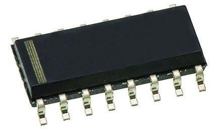
ICGOO电子元器件商城为您提供IL260-3E由NVE Corporation设计生产,在icgoo商城现货销售,并且可以通过原厂、代理商等渠道进行代购。 IL260-3E价格参考。NVE CorporationIL260-3E封装/规格:数字隔离器, 通用 数字隔离器 2500Vrms 5 通道 110Mbps 30kV/µs CMTI 16-SOIC(0.154",3.90mm 宽)。您可以下载IL260-3E参考资料、Datasheet数据手册功能说明书,资料中有IL260-3E 详细功能的应用电路图电压和使用方法及教程。
NVE Corp/Isolation Products的IL260-3E是一款数字隔离器,广泛应用于需要电气隔离的电子系统中。该型号的主要应用场景包括:

1. 工业自动化:在工业控制系统中,IL260-3E可用于隔离传感器、执行器和控制器之间的信号传输,防止高电压或电流干扰,确保系统的稳定性和安全性。例如,在PLC(可编程逻辑控制器)和分布式I/O模块之间提供可靠的隔离通信。

2. 电力系统:在电力监控和保护设备中,IL260-3E可以隔离高压侧和低压侧的信号,确保操作人员和设备的安全。它适用于智能电表、断路器、继电器等设备,保障数据准确传输的同时,避免高压对低电压电路的影响。

3. 医疗设备:在医疗仪器中,如心电图机、监护仪等,IL260-3E用于隔离患者接口与设备内部电路,确保患者和医护人员的安全,同时减少电磁干扰对测量结果的影响。

4. 通信设备:在通信基站、路由器和交换机等网络设备中,IL260-3E可以隔离不同电源域之间的信号,防止地线噪声和电压波动对通信质量的影响,确保数据传输的可靠性和稳定性。

5. 汽车电子:在电动汽车和混合动力汽车中,IL260-3E可用于隔离电池管理系统(BMS)、电机控制器和其他关键组件之间的信号,确保车辆电气系统的安全运行,避免高压直流电对低压控制电路的损害。

6. 消费电子产品:在一些高端消费电子产品中,如智能家居设备、音频放大器等,IL260-3E可以隔离输入输出端口与主控芯片之间的信号,提高产品的抗干扰能力和可靠性。

总之,IL260-3E凭借其高效、可靠的电气隔离性能,适用于多种需要信号隔离的场景,特别是在高电压、强电磁干扰环境下,能够有效保护电路和设备的安全,确保信号传输的稳定性和准确性。
| 参数 | 数值 |
| 产品目录 | |
| ChannelType | 单向 |
| 描述 | DGTL ISO 2.5KV GEN PURP 16SOIC |
| 产品分类 | |
| IsolatedPower | 无 |
| 品牌 | NVE Corp/Isolation Products |
| 数据手册 | |
| 产品图片 |
|
| 产品型号 | IL260-3E |
| PulseWidthDistortion(Max) | 3ns |
| rohs | 无铅 / 符合限制有害物质指令(RoHS)规范要求 |
| 产品系列 | IsoLoop® |
| 上升/下降时间(典型值) | 1ns, 1ns |
| 产品培训模块 | http://www.digikey.cn/PTM/IndividualPTM.page?site=cn&lang=zhs&ptm=25405 |
| 产品目录绘图 |
|
| 产品目录页面 | |
| 传播延迟tpLH/tpHL(最大值) | 15ns, 15ns |
| 供应商器件封装 | 16-SOIC N |
| 共模瞬态抗扰度(最小值) | 30kV/µs |
| 其它名称 | 390-1069-5 |
| 包装 | 管件 |
| 封装/外壳 | 16-SOIC(0.154",3.90mm 宽) |
| 工作温度 | -40°C ~ 85°C |
| 技术 | GMR(大型磁阻传感) |
| 数据速率 | 110Mbps |
| 标准包装 | 100 |
| 电压-电源 | 3 V ~ 5.5 V |
| 电压-隔离 | 2500Vrms |
| 类型 | 通用 |
| 脉宽失真(最大) | 3ns |
| 输入-输入侧1/输入侧2 | 5/0 |
| 通道数 | 5 |
| 通道类型 | 单向 |
| 隔离式电源 | 无 |


- 商务部:美国ITC正式对集成电路等产品启动337调查
- 曝三星4nm工艺存在良率问题 高通将骁龙8 Gen1或转产台积电
- 太阳诱电将投资9.5亿元在常州建新厂生产MLCC 预计2023年完工
- 英特尔发布欧洲新工厂建设计划 深化IDM 2.0 战略
- 台积电先进制程称霸业界 有大客户加持明年业绩稳了
- 达到5530亿美元!SIA预计今年全球半导体销售额将创下新高
- 英特尔拟将自动驾驶子公司Mobileye上市 估值或超500亿美元
- 三星加码芯片和SET,合并消费电子和移动部门,撤换高东真等 CEO
- 三星电子宣布重大人事变动 还合并消费电子和移动部门
- 海关总署:前11个月进口集成电路产品价值2.52万亿元 增长14.8%


PDF Datasheet 数据手册内容提取
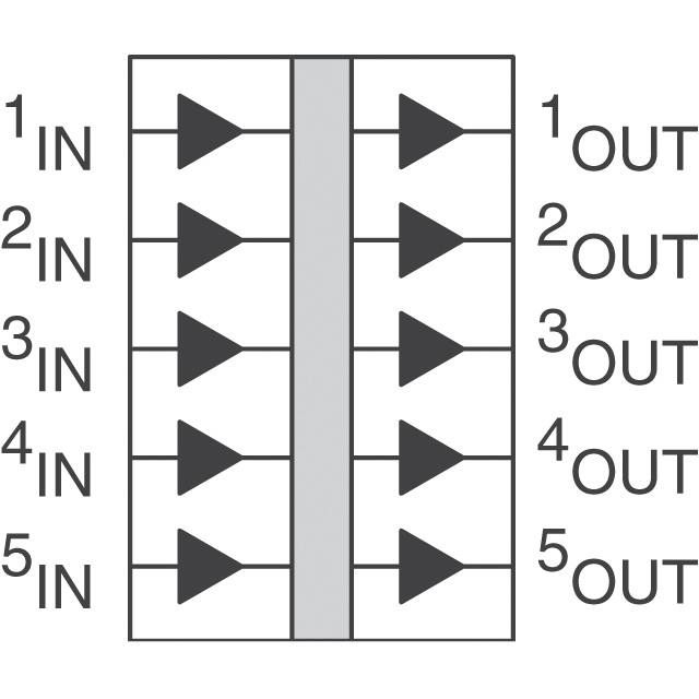
IL260/IL261/IL262 High Speed Five-Channel Digital Isolators Functional Diagrams Features • High Speed: 110 Mbps • 1.2 mA/channel typical quiescent current IL260-1140400 IN1 OUT1 • Very high isolation: 6 kVRMS Reinforced Isolation (V-Series) • High working voltage: 1 kV per VDE V 0884-10 (V-Series) RMS IN OUT • 50 kV/μs typ.; 30 kV/μs min. common mode transient immunity 2 2 • No carrier or clock for low EMI emissions and susceptibility IN OUT • −40°C to +85°C operating temperature 3 3 • 44000 year barrier life • Excellent magnetic immunity IN OUT 4 4 • 2 ns typical pulse width distortion • 100 ps pulse jitter IN OUT 5 5 • 4 ns typical propagation delay skew • 10 ns typical propagation delay IL260 • 2 ns channel-to-channel skew • VDE V 0884-10 certified; UL 1577 recognized • 0.15" and True 8™ mm 16-pin SOIC; 16-pin QSOP packages IN1 OUT1 Applications • ADCs and DACs IN2 OUT2 • Multiplexed data transmission • Board-to-board communication IN3 OUT3 • Peripheral interfaces • Equipment covered under IEC 61010-1 Edition 3 IN OUT • 5 kV rated IEC 60601-1 medical applications 4 4 RMS OUT IN Description 5 5 NVE’s IL260-Series five-channel high-speed digital isolators are CMOS devices manufactured with NVE’s patented* IsoLoop® IL261 spintronic Giant Magnetoresistive (GMR) technology. A unique ceramic/polymer composite barrier provides excellent isolation and virtually unlimited barrier life. IN OUT 1 1 All transmit and receive channels operate at 110 Mbps over the full temperature and supply voltage range. The symmetric magnetic IN OUT 2 2 coupling barrier provides a typical propagation delay of only 10 ns and a pulse width distortion of 2 ns, achieving the best specifications IN OUT of any isolator. The unique fifth channel can be is used to distribute 3 3 isolated clocks or handshake signals to multiple delta-sigma A/D OUT IN converters. High channel density makes these devices ideal for 4 4 isolating ADCs and DACs, parallel buses and peripheral interfaces. OUT IN Typical transient immunity of 50 kV/µs is unsurpassed. 5 5 Performance is specified over the temperature range of −40°C to +85°C without derating. IL262 The five-channel devices provide the highest channel density available. Parts are available in ultraminiature 16-pin QSOPs, as well as 0.15"and 0.3"-wide SOIC packages. V-Series versions offer extremely high isolation voltage of 6 kV . RMS IsoLoop is a registered trademark of NVE Corporation. REV. V *U.S. Patent number 5,831,426; 6,300,617 and others. NVE Corporation 11409 Valley View Road, Eden Prairie, MN 55344-3617 Phone: (952) 829-9217 Fax: (952) 829-9189 www.IsoLoop.com ©NVE Corporation
IL260/IL261/IL262 Absolute Maximum Ratings(1) Parameters Symbol Min. Typ. Max. Units Test Conditions Storage Temperature T −55 150 °C S Junction Temperature T −55 150 °C J Ambient Operating Temperature T −40 85 °C A Supply Voltage V ,V −0.5 7 V DD1 DD2 Input Voltage V −0.5 V + 0.5 V I DD Output Voltage V −0.5 V + 0.5 V O DD Output Current Drive I −10 10 mA O Lead Solder Temperature 260 °C 10 sec. ESD 2 kV HBM Recommended Operating Conditions Parameters Symbol Min. Typ. Max. Units Test Conditions Ambient Operating Temperature T −40 85 °C A Junction Temperature T −40 110 °C J Supply Voltage V ,V 3.0 5.5 V 3.3/5.0 V Operation DD1 DD2 Logic High Input Voltage V 2.4 V V IH DD Logic Low Input Voltage V 0 0.8 V IL Input Signal Rise and Fall Times t , t 1 μs IR IF Insulation Specifications Parameters Symbol Min. Typ. Max. Units Test Conditions QSOP 4.03 Creepage Distance 0.15'' SOIC 4.03 mm Per IEC 60601 (external) 0.3'' SOIC 8.03 8.3 Total Barrier Thickness (internal) 0.012 0.016 mm Leakage Current(5) 0.2 μA 240 V RMS RMS Barrier Resistance(5) R >1014 Ω 500 V IO Barrier Capacitance(5) C 5 pF f = 1 MHz IO Comparative Tracking Index CTI ≥600 V Per IEC 60112 RMS High Voltage Endurance AC 1000 V RMS At maximum (Maximum Barrier Voltage V IO operating temperature for Indefinite Life) DC 1500 V DC Surge Immunity (“V” Versions) V 12.8 kV Per IEC 61000-4-5 IOSM PK 100°C, 1000 V , 60% Barrier Life 44000 Years RMS CL activation energy Thermal Characteristics Parameter Symbol Min. Typ. Max. Units Test Conditions QSOP 60 Junction–Ambient 0.15" SOIC θ 60 °C/W Thermal Resistance JA Soldered to double- 0.3" SOIC 60 sided board; QSOP 10 Junction–Case (Top) free air 0.15" SOIC Ψ 10 °C/W Thermal Resistance JT 0.3" SOIC 20 QSOP 675 Power Dissipation 0.15" SOIC P 700 mW D 0.3" SOIC 800 2 NVE Corporation 11409 Valley View Road, Eden Prairie, MN 55344-3617 Phone: (952) 829-9217 Fax: (952) 829-9189 www.IsoLoop.com ©NVE Corporation
IL260/IL261/IL262 Safety and Approvals VDE V 0884-10 (VDE V 0884-11 pending) V-Series (Reinforced Isolation; VDE File Number 5016933-4880-0002) • Working Voltage (V ) 1000 V (1415 V ); reinforced insulation; pollution degree 2 IORM RMS PK • Isolation voltage (V ) 6000 V ISO RMS • Surge immunity (V ) 12.8 kV IOSM PK • Surge rating 8 kV • Transient overvoltage (V ) 6000 V IOTM PK • Each part tested at 2387 V for 1 second, 5 pC partial discharge limit PK • Samples tested at 6000 V for 60 sec.; then 2122 V for 10 sec. with 5 pC partial discharge limit PK PK Standard versions (Basic Isolation; VDE File Number 5016933-4880-0001) • Working Voltage (V ) 600 V (848 V ); basic insulation; pollution degree 2 IORM RMS PK • Isolation voltage (V ) 2500 V ISO RMS • Transient overvoltage (V ) 4000 V IOTM PK • Surge rating 4000 V • Each part tested at 1590 V for 1 second, 5 pC partial discharge limit PK • Samples tested at 4000 V for 60 sec.; then 1358 V for 10 sec. with 5 pC partial discharge limit PK PK Safety-Limiting Values Symbol Value Units Safety rating ambient temperature T 180 °C S Safety rating power (180°C) P 270 mW S Supply current safety rating (total of supplies) I 54 mA S IEC 61010-1 (Edition 2; TUV Certificate Numbers N1502812; N1502812-101) Reinforced Insulation; Pollution Degree II; Material Group III Part No. Working Suffix Package Voltage -1 QSOP 300 V RMS -3 0.15" SOIC 300 V RMS None 0.3" SOIC (standard) 300 V RMS V 0.3" SOIC (high isolation voltage) 1000 V RMS UL 1577 (Component Recognition Program File Number E207481) V-Series isolation grade 6 kV rating; tested at 7.2 kV (10.2 kV ) for 1 second; each lot sample tested at 6 kV (8485 V ) for 1 minute RMS PK RMS PK Standard isolation grade Each part tested at 3000 V (4243 V ) for 1 second; each lot sample tested at 2500 V (3536 V ) for 1 minute RMS PK RMS PK Soldering Profile Per JEDEC J-STD-020C, MSL 1 3 NVE Corporation 11409 Valley View Road, Eden Prairie, MN 55344-3617 Phone: (952) 829-9217 Fax: (952) 829-9189 www.IsoLoop.com ©NVE Corporation
IL260/IL261/IL262 IL260 Pin Connections 1 IN Input 1 1 2 GND Ground* IN V 1 1 DD2 3 IN Input 2 2 GND GND 4 IN Input 3 1 2 3 5 IN4 Input 4 IN OUT 2 1 6 V Supply Voltage 1 DD1 7 IN5 Input 5 IN3 OUT2 8 GND Ground* 1 9 GND Ground* IN OUT 2 4 3 10 OUT Output 5 5 V OUT 11 OUT Output 4 DD1 4 4 12 OUT Output 3 3 IN OUT 13 OUT Output 2 5 5 2 14 OUT1 Output 1 GND1 GND2 15 GND Ground* 2 16 V Supply Voltage 2 IL260 DD2 IL261 Pin Connections 1 V Supply Voltage 1 DD1 2 GND Ground* V V 1 DD1 DD2 3 IN Input 1 1 GND GND 4 IN Input 2 1 2 2 5 IN3 Input 3 IN OUT 1 1 6 IN Input 4 4 7 OUT5 Output 5 IN2 OUT2 8 GND Ground* 1 9 GND Ground* IN OUT 2 3 3 10 IN Input 5 5 IN OUT 11 OUT Output 4 4 4 4 12 OUT Output 3 3 OUT IN 13 OUT Output 2 5 5 2 14 OUT1 Output 1 GND1 GND2 15 GND Ground* 2 16 V Supply Voltage 2 IL261 DD2 IL262 Pin Connections 1 V Supply Voltage 1 DD1 2 GND Ground* V V 1 DD1 DD2 3 IN Input 1 1 GND GND 4 IN Input 2 1 2 2 5 IN Input 3 3 IN OUT 1 1 6 OUT Output 4 4 7 OUT5 Output 5 IN2 OUT2 8 GND Ground* 1 9 GND Ground* IN OUT 2 3 3 10 IN Input 5 5 OUT IN 11 IN Input 4 4 4 4 12 OUT Output 3 3 OUT IN 13 OUT Output 2 5 5 2 14 OUT1 Output 1 GND1 GND2 15 GND Ground* 2 16 V Supply Voltage 2 IL262 DD2 *NOTE: Pins 2 and 8 are internally connected, as are pins 9 and 15. 4 NVE Corporation 11409 Valley View Road, Eden Prairie, MN 55344-3617 Phone: (952) 829-9217 Fax: (952) 829-9189 www.IsoLoop.com ©NVE Corporation
IL260/IL261/IL262 3.3 Volt Electrical Specifications (T to T ) min max Parameters Symbol Min. Typ. Max. Units Test Conditions IL260 300 400 μA Input Quiescent Current IL261 I 1.2 1.75 mA DD1 IL262 2.4 3.5 mA IL260 6 8.75 mA Output Quiescent Current IL261 I 4.8 7 mA DD2 IL262 3.6 5.25 mA Logic Input Current I −10 10 μA i V −0.1 V I = −20 μA, V=V Logic High Output Voltage V DD DD V O I IH OH 0.8 x V 0.9 x V I = −4 mA, V=V DD DD O I IH 0 0.1 I = 20 μA, V=V Logic Low Output Voltage V V O I IL OL 0.5 0.8 I = 4 mA, V=V O I IL Switching Specifications (V = 3.3 V) DD Maximum Data Rate 100 110 Mbps C = 15 pF L Minimum Pulse Width(7) PW 10 ns 50% Points, V O Propagation Delay Input to Output t 12 18 ns C = 15 pF (High to Low) PHL L Propagation Delay Input to Output t 12 18 ns C = 15 pF (Low to High) PLH L Pulse Width Distortion |t −t |(2) PWD 2 3 ns C = 15 pF PHL PLH L Propagation Delay Skew(3) t 4 6 ns C = 15 pF PSK L Output Rise Time (10%–90%) t 2 4 ns C = 15 pF R L Output Fall Time (10%–90%) t 2 4 ns C = 15 pF F L Common Mode Transient Immunity V = 1500 V |CM |,|CM | 30 50 kV/μs CM DC (Output Logic High to Logic Low)(4) H L t = 25 ns TRANSIENT Channel-to-Channel Skew 2 3 ns C = 15 pF L Dynamic Power Consumption(6) 140 240 μA/Mbps per channel Magnetic Field Immunity(8) (V = 3V, 3V<V <5.5V) DD2 DD1 Power Frequency Magnetic Immunity H 1000 1500 A/m 50Hz/60Hz PF Pulse Magnetic Field Immunity H 1800 2000 A/m t = 8µs PM p Damped Oscillatory Magnetic Field H 1800 2000 A/m 0.1Hz – 1MHz OSC Cross-axis Immunity Multiplier(9) K 2.5 X 5 NVE Corporation 11409 Valley View Road, Eden Prairie, MN 55344-3617 Phone: (952) 829-9217 Fax: (952) 829-9189 www.IsoLoop.com ©NVE Corporation
IL260/IL261/IL262 5 Volt Electrical Specifications (T to T ) min max Parameters Symbol Min. Typ. Max. Units Test Conditions IL260 350 500 μA Input Quiescent Current IL261 I 1.8 2.5 mA DD1 IL262 3.6 5 mA IL260 9 12.5 mA Output Quiescent Current IL261 I 7.2 10 mA DD2 IL262 5.4 7.5 mA Logic Input Current I −10 10 μA i V −0.1 V I = −20 μA, V = V Logic High Output Voltage V DD DD V O I IH OH 0.8 x V 0.9 x V I = −4 mA, V = V DD DD O I IH 0 0.1 I = 20 μA, V = V Logic Low Output Voltage V V O I IL OL 0.5 0.8 I = 4 mA, V = V O I IL Switching Specifications (V = 5 V) DD Maximum Data Rate 100 110 Mbps C = 15 pF L Minimum Pulse Width(7) PW 10 ns 50% Points, V O Propagation Delay Input to Output t 10 15 ns C = 15 pF (High to Low) PHL L Propagation Delay Input to Output t 10 15 ns C = 15 pF (Low to High) PLH L Pulse Width Distortion |t −t |(2) PWD 2 3 ns C = 15 pF PHL PLH L Pulse Jitter(10) t 100 ps C = 15 pF J L Propagation Delay Skew(3) t 4 6 ns C = 15 pF PSK L Output Rise Time (10%–90%) t 1 3 ns C = 15 pF R L Output Fall Time (10%–90%) t 1 3 ns C = 15 pF F L Common Mode Transient Immunity V = 1500 V |CM |,|CM | 30 50 kV/μs CM DC (Output Logic High to Logic Low)(4) H L t = 25 ns TRANSIENT Channel-to-Channel Skew 2 3 ns C = 15 pF L Dynamic Power Consumption(6) 200 340 μA/Mbps per channel Magnetic Field Immunity(8) (V = 5V, 3V<V <5.5V) DD2 DD1 Power Frequency Magnetic Immunity H 2800 3500 A/m 50Hz/60Hz PF Pulse Magnetic Field Immunity H 4000 4500 A/m t = 8µs PM p Damped Oscillatory Magnetic Field H 4000 4500 A/m 0.1Hz – 1MHz OSC Cross-axis Immunity Multiplier(9) K 2.5 X Notes (apply to both 3.3 V and 5 V specifications): 1. Absolute maximum means the device will not be damaged if operated under these conditions. It does not guarantee performance. 2. PWD is defined as |t − t |. %PWD is equal to PWD divided by pulse width. PHL PLH 3. t is the magnitude of the worst-case difference in t and/or t between devices at 25°C. PSK PHL PLH 4. CM is the maximum common mode voltage slew rate that can be sustained while maintaining V > 0.8 V . CM is the maximum H O DD2 L common mode input voltage that can be sustained while maintaining V < 0.8 V. The common mode voltage slew rates apply to both rising O and falling common mode voltage edges. 5. Device is considered a two terminal device: pins 1–8 shorted and pins 9–16 shorted. 6. Dynamic power consumption numbers are calculated per channel and are supplied by the channel’s input side power supply. 7. Minimum pulse width is the minimum value at which specified PWD is guaranteed. 8. The relevant test and measurement methods are given in the Electromagnetic Compatibility section on p. 6. 9. External magnetic field immunity is improved by this factor if the field direction is “end-to-end” rather than to “pin-to-pin” (see diagram on p. 6). 10. 66,535-bit pseudo-random binary signal (PRBS) NRZ bit pattern with no more than five consecutive 1s or 0s; 800 ps transition time. 6 NVE Corporation 11409 Valley View Road, Eden Prairie, MN 55344-3617 Phone: (952) 829-9217 Fax: (952) 829-9189 www.IsoLoop.com ©NVE Corporation
IL260/IL261/IL262 Application Information Electrostatic Discharge Sensitivity Thermal Management This product has been tested for electrostatic sensitivity to the IsoLoop Isolators are designed for low power dissipation and limits stated in the specifications. However, NVE recommends that thermal performance, providing unmatched channel density for all integrated circuits be handled with appropriate care to avoid high-performance isolators. Nevertheless, package temperature rise damage. Damage caused by inappropriate handling or storage could should be considered when running multiple channels at high range from performance degradation to complete failure. speed. Power consumption is higher at 5 volt operation than at 3.3 volts, and dynamic supply current is higher on the input side of Electromagnetic Compatibility the isolators than the output side, so thermal management is more IsoLoop Isolators have the lowest EMC footprint of any isolation important with five-volt input-side power supplies. technology. There are no internal clocks or carriers. IsoLoop Isolators’ Wheatstone bridge configuration and differential IL260/IL261/IL262 parts have a maximum junction temperature of magnetic field signaling ensure excellent EMC performance against 110°C. Based on the specifications contained in this datasheet, the all relevant standards. derating curve at typical operating conditions is as follows: These isolators are fully compliant with generic EMC standards EN50081, EN50082-1 and the umbrella line-voltage standard for Information Technology Equipment (ITE) EN61000. NVE has completed compliance tests in the categories below: (cid:31) EN50081-1 Residential, Commercial & Light Industrial Methods EN55022, EN55014 EN50082-2: Industrial Environment Methods EN61000-4-2 (ESD), EN61000-4-3 (Electromagnetic Field Immunity), EN61000-4-4 (Electrical Transient Immunity), EN61000-4-6 (RFI Immunity), EN61000-4-8 (Power Frequency Magnetic Field Immunity), EN61000-4-9 (Pulsed Magnetic Field), EN61000-4-10 (Damped Oscillatory Magnetic Field) ENV50204 Radiated Field from Digital Telephones (Immunity Test) Immunity to external magnetic fields is even higher if the field direction is “end-to-end” rather than to “pin-to-pin” as shown in the Power Supply Decoupling diagram below: Both power supplies to these devices should be decoupled with low ESR 47 nF ceramic capacitors. Ground planes for both GND and 1 GND are highly recommended for data rates above 10 Mbps. 2 Capacitors must be located as close as possible to the V pins. DD Maintaining Creepage Creepage distances are often critical in isolated circuits. In addition to meeting JEDEC standards, NVE isolator packages have unique creepage specifications. Standard pad libraries often extend under the package, compromising creepage and clearance. Similarly, ground planes, if used, should be spaced to avoid compromising Cross-axis Field Direction clearance. Package drawings and recommended pad layouts are included in this datasheet. Dynamic Power Consumption IsoLoop Isolators achieve their low power consumption from the Signal Status on Start-up and Shut Down way they transmit data across the isolation barrier. By detecting the To minimize power dissipation, input signals are differentiated and edge transitions of the input logic signal and converting these to then latched on the output side of the isolation barrier to reconstruct narrow current pulses, a magnetic field is created around the GMR the signal. This could result in an ambiguous output state Wheatstone bridge. Depending on the direction of the magnetic depending on power up, shutdown and power loss sequencing. field, the bridge causes the output comparator to switch following Therefore, the designer should consider including an initialization the input logic signal. Since the current pulses are narrow, about signal in the start-up circuit. Initialization consists of toggling the 2.5 ns, the power consumption is independent of mark-to-space input either high then low, or low then high. ratio and solely dependent on frequency. This has obvious advantages over optocouplers, which have power consumption heavily dependent on mark-to-space ratio. 7 NVE Corporation 11409 Valley View Road, Eden Prairie, MN 55344-3617 Phone: (952) 829-9217 Fax: (952) 829-9189 www.IsoLoop.com ©NVE Corporation
IL260/IL261/IL262 Application Diagram—Multi-Channel Delta-Sigma A/D Converter In a typical single-channel delta-sigma ADC, the system clock is located on the isolated side of the system and only four channels of isolation are required. With multiple ADCs configured in a channel-to-channel isolation configuration, however, clock jitter and edge placement accuracy of the system clock must be matched between ADCs. The best solution is to use a single clock on the system side and distribute the clock to each ADC. The five-channel IL261 is ideal, with the fifth channel used to distribute a single, isolated clock to multiple ADCs as shown below: Bridge Bias Delta Sigma A/D CS5532 Bridge + Bridge - Isolation Boundary Serial Data Out Iso SD Out Serial Data In Iso SD In Clock Data Clock Iso Data Clock Generator Chip Select Iso CS Channel 1 IL261 OSC 2 Bridge Bias Delta Sigma A/D CS5532 Bridge + Bridge - Serial Data Out Iso SD Out Serial Data In Iso SD In Channel n Data Clock Iso Data Clock Chip Select Iso CS IL261 OSC 2 8 NVE Corporation 11409 Valley View Road, Eden Prairie, MN 55344-3617 Phone: (952) 829-9217 Fax: (952) 829-9189 www.IsoLoop.com ©NVE Corporation
IL260/IL261/IL262 Package Drawings Ultraminiature 16-pin QSOP Package (-1 suffix) Dimensions in inches (mm); scale = approx. 5X 0.188 (4.77) 0.020 (0.50) 0.197 (5.00) 0.029 (0.75) 0.050 (1.27) 0.060 (1.52) 0.056 (1.42) 0.069 (1.75) 0.228 (5.8) 0.150 (3.8) 0.244 (6.2) 0.157 (4.0) 0.004 (0.10) 0.025 (0.635) 0.010 (0.25) NOM NOTE:Pin spacing is a BASIC dimension; tolerances 0.009 (0.2) 0.007 (0.20) do not accumulate 0.012 (0.3) 0.010 (0.25) 0.15" 16-pin SOIC Package (-3 suffix) Dimensions in inches (mm); scale = approx. 5X 0.013 (0.3) NOM 0.020 (0.5) 0.007 (0.2) 0.016 (0.4) 0.013 (0.3) 0.050 (1.3) 0.386 (9.8) 0.394 (10.0) Pin 1 identified by either an 0.055 (1.40) 0.054 (1.4) indent or a 0.062 (1.58) 0.072 (1.8) marked dot 0.150 (3.81) 0.049 (1.24) 0.004 (0.1) 0.157 (3.99) 0.051 (1.30) 0.012 (0.3) 0.228 (5.8) NOTE:Pin spacing is a BASIC dimension; tolerances 0.244 (6.2) do not accumulate 9 NVE Corporation 11409 Valley View Road, Eden Prairie, MN 55344-3617 Phone: (952) 829-9217 Fax: (952) 829-9189 www.IsoLoop.com ©NVE Corporation
IL260/IL261/IL262 0.3" 16-pin SOIC Package (no suffix) Dimensions in inches (mm); scale = approx. 5X 0.033 (0.85)* 0.260 (6.60)* 0.043 (1.10) 0.280 (7.11) 0.013 (0.3) 0.020 (0.5) 0.007 (0.2) 0.007 (0.18)* 0.016 (0.4) 0.397 (10.08) 0.013 (0.3) 0.010 (0.25) 0.050 (1.3) 0.413 (10.49) 0.092 (2.34) Pin 1 identified by 0.105 (2.67) either an indent or a marked dot 0.017 (0.43)* 0.08 (2.0) 0.022 (0.56) 0.10 (2.5) 0.292 (7.42)* 0.049 (1.24) 0.004 (0.1) 0.299 (7.59) 0.051 (1.30) 0.012 (0.3) 0.394 (10.00) NOTE:Pin spacing is a BASIC 0.419 (10.64) dimension; tolerances do not accumulate *Specified for True 8™ package to guarantee 8 mm creepage per IEC 60601. 10 NVE Corporation 11409 Valley View Road, Eden Prairie, MN 55344-3617 Phone: (952) 829-9217 Fax: (952) 829-9189 www.IsoLoop.com ©NVE Corporation
IL260/IL261/IL262 Recommended Pad Layouts 4 mm x 5 mm 16-pin QSOP Pad Layout Dimensions in inches (mm); scale = approx. 5X 0.160 (4.05) 0.025 (0.635) 0.012 (0.30) 16 PLCS 0.275 (6.99) 0.15" 16-pin SOIC Pad Layout Dimensions in inches (mm); scale = approx. 5X 0.160 (4.06) 0.050 (1.27) 0.020 (0.51) 16 PLCS 0.275 (6.99) 11 NVE Corporation 11409 Valley View Road, Eden Prairie, MN 55344-3617 Phone: (952) 829-9217 Fax: (952) 829-9189 www.IsoLoop.com ©NVE Corporation
IL260/IL261/IL262 0.3" 16-pin SOIC Pad Layout Dimensions in inches (mm); scale = approx. 5X 0.317 (8.05) 0.050 (1.27) 0.020 (0.51) 16 PLCS 0.449 (11.40) 12 NVE Corporation 11409 Valley View Road, Eden Prairie, MN 55344-3617 Phone: (952) 829-9217 Fax: (952) 829-9189 www.IsoLoop.com ©NVE Corporation
IL260/IL261/IL262 Available Parts Isolation Available Transmit Receive Voltage Parts Channels Channels (RMS) Package IL260-1E 5 0 2.5 kV QSOP IL260-3E 5 0 2.5 kV Narrow SOIC IL260E 5 0 2.5 kV Wide SOIC IL260VE 5 0 6 kV Wide SOIC IL261-1E 4 1 2.5 kV QSOP IL261-3E 4 1 2.5 kV Narrow SOIC IL261E 4 1 2.5 kV Wide SOIC IL261VE 4 1 6 kV Wide SOIC IL262-3E 3 2 2.5 kV Narrow SOIC IL262E 3 2 2.5 kV Wide SOIC IL262VE 3 2 6 kV Wide SOIC All part types are available on tape and reel. Ordering Information IL 260 V - 3 E TR13 Valid Part Numbers IL260 IL260E Bulk Package IL260VE Blank = Tube IL260-1E TR7 = 7'' Tape and Reel IL260-3 TR13 = 13'' Tape and Reel IL260-3E IL261 Package IL261E Blank = 80/20 Tin/Lead Plating IL261VE E = RoHS Compliant IL261-1E IL261-3 Package Type IL261-3E Blank = 0.3" 16-pin SOIC IL262 -1 = 0.15'' 16-pin QSOP IL262E -3 = 0.15'' 16-pin SOIC IL262VE IL262-3 Grade IL262-3E Blank = Standard Isolation Voltage (2.5 kV) All IL260-Series part V = High Isolation types are available on Voltage (6 kV) tape and reel. Base Part Number 260 = 5 Transmit Channels 261 = 4 Transmit Channels; 1 Receive Channel 262 = 3 Transmit Channels; 2 Receive Channel Product Family IL = Isolators RoHS COMPLIANT 13 NVE Corporation 11409 Valley View Road, Eden Prairie, MN 55344-3617 Phone: (952) 829-9217 Fax: (952) 829-9189 www.IsoLoop.com ©NVE Corporation
IL260/IL261/IL262 Revision History ISB-DS-001-IL260/1/2-V Change November 2016 • VDE certification and UL approval for V-Series versions (6 kV reinforced isolation). ISB-DS-001-IL260/1/2-U Changes • Updated VDE certification standard to VDE V 0884-10. • Upgraded “VE” Version Surge Immunity specification to 12.8 kV. • Upgraded “VE” Version VDE 0884-10 rating to reinforced insulation. • Corrected QSOP pin width dimension (p. 10). ISB-DS-001-IL260/1/2-T Changes • Increased V-Series isolation voltage to 6 kVrms. • Increased typ. Total Barrier Thickness specification to 0.016 mm. • Increased CTI min. specification to ≥600 V . RMS ISB-DS-001-IL260/1/2-S Changes • Added V-Series 5 kV isolation voltage versions. • More detailed “Available Parts” table. ISB-DS-001-IL260/1/2-R Changes • Added QSOP packages (-1 suffix). • Revised and added details to thermal characteristic specifications (p. 2). • Added VDE 0884 Safety-Limiting Values (p. 3). • Added “Thermal Management” paragraph in Applications section. ISB-DS-001-IL260/1/2-Q Change • IEC 60747-5-5 (VDE 0884) certification. ISB-DS-001-IL260/1/2-P Changes • Tighter quiescent current specifications. • Upgraded from MSL 2 to MSL 1. ISB-DS-001-IL260/1/2-O Changes • Increased transient immunity specifications based on additional data. • Added VDE 0884 pending. • Added high voltage endurance specifications. • Increased magnetic immunity specifications. • Updated package drawings. • Added recommended solder pad layouts. 14 NVE Corporation 11409 Valley View Road, Eden Prairie, MN 55344-3617 Phone: (952) 829-9217 Fax: (952) 829-9189 www.IsoLoop.com ©NVE Corporation
IL260/IL261/IL262 Datasheet Limitations The information and data provided in datasheets shall define the specification of the product as agreed between NVE and its customer, unless NVE and customer have explicitly agreed otherwise in writing. All specifications are based on NVE test protocols. In no event however, shall an agreement be valid in which the NVE product is deemed to offer functions and qualities beyond those described in the datasheet. Limited Warranty and Liability Information in this document is believed to be accurate and reliable. However, NVE does not give any representations or warranties, expressed or implied, as to the accuracy or completeness of such information and shall have no liability for the consequences of use of such information. In no event shall NVE be liable for any indirect, incidental, punitive, special or consequential damages (including, without limitation, lost profits, lost savings, business interruption, costs related to the removal or replacement of any products or rework charges) whether or not such damages are based on tort (including negligence), warranty, breach of contract or any other legal theory. Right to Make Changes NVE reserves the right to make changes to information published in this document including, without limitation, specifications and product descriptions at any time and without notice. This document supersedes and replaces all information supplied prior to its publication. Use in Life-Critical or Safety-Critical Applications Unless NVE and a customer explicitly agree otherwise in writing, NVE products are not designed, authorized or warranted to be suitable for use in life support, life-critical or safety-critical devices or equipment. NVE accepts no liability for inclusion or use of NVE products in such applications and such inclusion or use is at the customer’s own risk. Should the customer use NVE products for such application whether authorized by NVE or not, the customer shall indemnify and hold NVE harmless against all claims and damages. Applications Applications described in this datasheet are illustrative only. NVE makes no representation or warranty that such applications will be suitable for the specified use without further testing or modification. Customers are responsible for the design and operation of their applications and products using NVE products, and NVE accepts no liability for any assistance with applications or customer product design. It is customer’s sole responsibility to determine whether the NVE product is suitable and fit for the customer’s applications and products planned, as well as for the planned application and use of customer’s third party customers. Customers should provide appropriate design and operating safeguards to minimize the risks associated with their applications and products. NVE does not accept any liability related to any default, damage, costs or problem which is based on any weakness or default in the customer’s applications or products, or the application or use by customer’s third party customers. The customer is responsible for all necessary testing for the customer’s applications and products using NVE products in order to avoid a default of the applications and the products or of the application or use by customer’s third party customers. NVE accepts no liability in this respect. Limiting Values Stress above one or more limiting values (as defined in the Absolute Maximum Ratings System of IEC 60134) will cause permanent damage to the device. Limiting values are stress ratings only and operation of the device at these or any other conditions above those given in the recommended operating conditions of the datasheet is not warranted. Constant or repeated exposure to limiting values will permanently and irreversibly affect the quality and reliability of the device. Terms and Conditions of Sale In case an individual agreement is concluded only the terms and conditions of the respective agreement shall apply. NVE hereby expressly objects to applying the customer’s general terms and conditions with regard to the purchase of NVE products by customer. No Offer to Sell or License Nothing in this document may be interpreted or construed as an offer to sell products that is open for acceptance or the grant, conveyance or implication of any license under any copyrights, patents or other industrial or intellectual property rights. Export Control This document as well as the items described herein may be subject to export control regulations. Export might require a prior authorization from national authorities. Automotive Qualified Products Unless the datasheet expressly states that a specific NVE product is automotive qualified, the product is not suitable for automotive use. It is neither qualified nor tested in accordance with automotive testing or application requirements. NVE accepts no liability for inclusion or use of non-automotive qualified products in automotive equipment or applications. In the event that customer uses the product for design-in and use in automotive applications to automotive specifications and standards, customer (a) shall use the product without NVE’s warranty of the product for such automotive applications, use and specifications, and (b) whenever customer uses the product for automotive applications beyond NVE’s specifications such use shall be solely at customer’s own risk, and (c) customer fully indemnifies NVE for any liability, damages or failed product claims resulting from customer design and use of the product for automotive applications beyond NVE’s standard warranty and NVE’s product specifications. 15 NVE Corporation 11409 Valley View Road, Eden Prairie, MN 55344-3617 Phone: (952) 829-9217 Fax: (952) 829-9189 www.IsoLoop.com ©NVE Corporation
IL260/IL261/IL262 An ISO 9001 Certified Company NVE Corporation 11409 Valley View Road Eden Prairie, MN 55344-3617 USA Telephone: (952) 829-9217 Fax: (952) 829-9189 www.nve.com e-mail: iso-info@nve.com ©NVE Corporation All rights are reserved. Reproduction in whole or in part is prohibited without the prior written consent of the copyright owner. ISB-DS-001-IL260/1/2-V November 2016 16 NVE Corporation 11409 Valley View Road, Eden Prairie, MN 55344-3617 Phone: (952) 829-9217 Fax: (952) 829-9189 www.IsoLoop.com ©NVE Corporation