ICGOO在线商城 > 集成电路(IC) > 时钟/计时 - 可编程计时器和振荡器 > ICM7555CBAZ-T

 Datasheet下载
- 型号: ICM7555CBAZ-T
- 制造商: Intersil
- 库位|库存: xxxx|xxxx
- 要求:
| 数量阶梯 | 香港交货 | 国内含税 |
| +xxxx | $xxxx | ¥xxxx |
查看当月历史价格
查看今年历史价格
ICM7555CBAZ-T产品简介:
ICGOO电子元器件商城为您提供ICM7555CBAZ-T由Intersil设计生产,在icgoo商城现货销售,并且可以通过原厂、代理商等渠道进行代购。 ICM7555CBAZ-T价格参考。IntersilICM7555CBAZ-T封装/规格:时钟/计时 - 可编程计时器和振荡器, 555 Type, Timer/Oscillator (Single) IC 1MHz 8-SOIC。您可以下载ICM7555CBAZ-T参考资料、Datasheet数据手册功能说明书,资料中有ICM7555CBAZ-T 详细功能的应用电路图电压和使用方法及教程。
ICM7555CBAZ-T是瑞萨电子(Renesas Electronics America Inc.)生产的一款CMOS工艺的可编程定时器,属于时钟/计时类中的可编程计时器和振荡器。该器件是经典555定时器的低功耗、高精度CMOS版本,具有与传统双极型555引脚兼容的特点,但功耗更低、输入阻抗更高、温度稳定性更好。

ICM7555CBAZ-T广泛应用于需要精确时间控制或脉冲生成的电子系统中。典型应用场景包括:定时延时电路(如自动关断、延时启动)、脉冲发生器、LED闪烁控制、频率分频、电源管理中的时序控制、传感器信号调理电路中的单稳态或多谐振荡模式,以及便携式设备中的低功耗定时功能。由于其宽工作电压范围(通常为2.1V至18V)和出色的抗干扰能力,该器件适用于电池供电设备、工业控制、消费电子、医疗仪器及汽车电子等对可靠性和能效要求较高的场合。

此外,ICM7555CBAZ-T采用小型化封装(如SOIC),便于在空间受限的PCB设计中使用,适合现代紧凑型电子产品。其稳定的工作性能和广泛的适用性使其成为替代传统555定时器的理想选择。
| 参数 | 数值 |
| 产品目录 | 集成电路 (IC)半导体 |
| 描述 | IC OSC SINGLE TIMER 1MHZ 8-SOIC计时器和支持产品 GEN PUR CMOS TIMER 8 COM |
| 产品分类 | |
| 品牌 | Intersil |
| 产品手册 | |
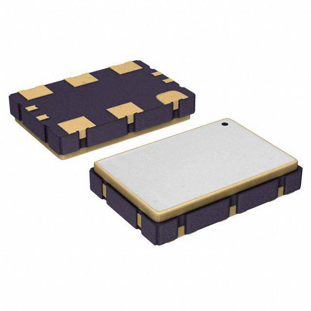
| 产品图片 |
|
| rohs | 符合RoHS无铅 / 符合限制有害物质指令(RoHS)规范要求 |
| 产品系列 | 时钟和计时器IC,计时器和支持产品,Intersil ICM7555CBAZ-T- |
| 数据手册 | |
| 产品型号 | ICM7555CBAZ-T |
| PCN组件/产地 | |
| 产品种类 | 计时器和支持产品 |
| 供应商器件封装 | 8-SOIC |
| 其它名称 | ICM7555CBAZ-TCT |
| 内部定时器数量 | 2 |
| 包装 | 剪切带 (CT) |
| 商标 | Intersil |
| 安装类型 | 表面贴装 |
| 安装风格 | SMD/SMT |
| 封装 | Reel |
| 封装/外壳 | 8-SOIC(0.154",3.90mm 宽) |
| 封装/箱体 | SOIC-8 |
| 工作温度 | 0°C ~ 70°C |
| 工厂包装数量 | 2500 |
| 最大工作温度 | + 70 C |
| 最小工作温度 | 0 C |
| 标准包装 | 1 |
| 电压-电源 | 2 V ~ 18 V |
| 电流-电源 | 60µA |
| 电源电压-最大 | 18 V |
| 电源电压-最小 | 2 V |
| 类型 | 555 型,计时器/振荡器(单路) |
| 系列 | ICM7555 |
| 计数 | - |
| 频率 | 1MHz |


- 商务部:美国ITC正式对集成电路等产品启动337调查
- 曝三星4nm工艺存在良率问题 高通将骁龙8 Gen1或转产台积电
- 太阳诱电将投资9.5亿元在常州建新厂生产MLCC 预计2023年完工
- 英特尔发布欧洲新工厂建设计划 深化IDM 2.0 战略
- 台积电先进制程称霸业界 有大客户加持明年业绩稳了
- 达到5530亿美元!SIA预计今年全球半导体销售额将创下新高
- 英特尔拟将自动驾驶子公司Mobileye上市 估值或超500亿美元
- 三星加码芯片和SET,合并消费电子和移动部门,撤换高东真等 CEO
- 三星电子宣布重大人事变动 还合并消费电子和移动部门
- 海关总署:前11个月进口集成电路产品价值2.52万亿元 增长14.8%


PDF Datasheet 数据手册内容提取
DATASHEET ICM7555, ICM7556 FN2867 General Purpose Timers Rev 1.00 June 28, 2016 The ICM7555 and ICM7556 are CMOS RC timers providing Features significantly improved performance over the standard SE/NE555/556 and 355 timers, while at the same time being • Exact equivalent in most cases for SE/NE 555/556 or direct replacements for those devices in most applications. TLC555/556 Improved parameters include low supply current, wide • Low supply current operating supply voltage range, low Threshold, Trigger and - ICM7555. . . . . . . . . . . . . . . . . . . . . . . . . . . . . . . . . . . . . 60µA Reset currents, no crowbarring of the supply current during - ICM7556. . . . . . . . . . . . . . . . . . . . . . . . . . . . . . . . . . . 120µA output transitions, higher frequency performance and no requirement to decouple Control Voltage for stable operation. • Extremely low input currents . . . . . . . . . . . . . . . . . . . . . . 20pA Specifically, the ICM7555 and ICM7556 are stable controllers • High speed operation . . . . . . . . . . . . . . . . . . . . . . . . . . . .1MHz capable of producing accurate time delays or frequencies. The • Guaranteed supply voltage range . . . . . . . . . . . . . . 2V to 18V ICM7556 is a dual ICM7555, with the two timers operating • Temperature stability . . . . . . . . . . . . . 0.005%/°C at +25°C independently of each other, sharing only V+ and GND. In the one shot mode, the pulse width of each circuit is precisely • Normal reset function - no crowbarring of supply during controlled by one external resistor and capacitor. For astable output transition operation as an oscillator, the free running frequency and the • Can be used with higher impedance timing elements than duty cycle are both accurately controlled by two external regular 555/556 for longer RC time constants resistors and one capacitor. Unlike the regular bipolar SE/NE555/556 devices, the Control Voltage terminal need not • Timing from microseconds through hours be decoupled with a capacitor. The circuits are triggered and • Operates in both astable and monostable modes reset on falling (negative) waveforms, and the output inverter • Adjustable duty cycle can source or sink currents large enough to drive TTL loads, or provide minimal offsets to drive CMOS loads. • High output source/sink driver can drive TTL/CMOS • Outputs have very low offsets, HIGH and LOW • Pb-free (RoHS Compliant) Applications • Precision timing • Pulse generation • Sequential timing • Time delay generation • Pulse width modulation • Pulse position modulation • Missing pulse detector Pin Configurations ICM7555 ICM7556 (8 LD PDIP, SOIC) (14 LD PDIP, CERDIP) TOP VIEW TOP VIEW DISCHARGE1 1 14 VDD THRESHOLD1 2 13 DISCHARGE2 GND 1 8 VDD CONTROL 3 12 THRESHOLD2 TRIGGER 2 7 DISCHARGE VOLTAGE1 CONTROL RESET1 4 11 OUTPUT 3 6 THRESHOLD VOLTAGE2 OUTPUT1 5 10 RESET2 RESET 4 5 CONTROL VOLTAGE TRIGGER1 6 9 OUTPUT2 GND 7 8 TRIGGER2 FN2867 Rev 1.00 Page 1 of 13 June 28, 2016
ICM7555, ICM7556 Ordering Information TEMP. RANGE TAPE AND REEL PACKAGE PART NUMBER PART MARKING (°C) (UNITS) (RoHS COMPLIANT) PKG. DWG. # ICM7555CBAZ (Notes2, 3) 7555 CBAZ 0 to +70 8 Ld SOIC M8.15 ICM7555CBAZ-T (Notes1, 2, 3) 7555 CBAZ 0 to +70 2.5k 8 Ld SOIC (Tape and Reel) M8.15 ICM7555IBAZ (Notes2, 3) 7555 IBAZ -25 to +85 8 Ld SOIC M8.15 ICM7555IBAZ-T (Notes1, 2, 3) 7555 IBAZ -25 to +85 2.5k 8 Ld SOIC (Tape and Reel) M8.15 ICM7555IPAZ (Notes2, 3) 7555 IPAZ -25 to +85 8 Ld PDIP E8.3 ICM7556IPDZ (Notes2, 3) ICM7556IPDZ -25 to +85 14 Ld PDIP E14.3 ICM7556MJD ICM7556MJD -55 to +125 14 Ld Cerdip F14.3 (No longer available or supported) NOTES: 1. Please refer to TB347 for details on reel specifications. 2. These Intersil Pb-free plastic packaged products employ special Pb-free material sets, molding compounds/die attach materials, and 100% matte tin plate plus anneal (e3 termination finish, which is RoHS compliant and compatible with both SnPb and Pb-free soldering operations). Intersil Pb-free products are MSL classified at Pb-free peak reflow temperatures that meet or exceed the Pb-free requirements of IPC/JEDEC J STD-020. 3. For Moisture Sensitivity Level (MSL), please see product information page for ICM7555, ICM7556. For more information on MSL, please see tech brief TB363. FN2867 Rev 1.00 Page 2 of 13 June 28, 2016
ICM7555, ICM7556 Absolute Maximum Ratings Thermal Information Supply Voltage . . . . . . . . . . . . . . . . . . . . . . . . . . . . . . . . . . . . . . . . . . . . .+18V Thermal Resistance (Typical, Notes5, 6) JA (°C/W) JC (°C/W) Input Voltage 14 Ld CERDIP Package. . . . . . . . . . . . . . . 80 24 Trigger, Control Voltage, Threshold, 14 Ld PDIP Package* . . . . . . . . . . . . . . . . 115 46 Reset (Note4). . . . . . . . . . . . . . . . . . . . . . . . . . . . . V+ +0.3V to GND -0.3V 8 Ld PDIP Package* . . . . . . . . . . . . . . . . . 130 69 Output Current . . . . . . . . . . . . . . . . . . . . . . . . . . . . . . . . . . . . . . . . . . . 100mA 8 Ld SOIC Package. . . . . . . . . . . . . . . . . . . 170 67 Maximum Junction Temperature (Hermetic Package) . . . . . . . . . . . .+175°C Operating Conditions Maximum Junction Temperature (Plastic Package) . . . . . . . . . . . .+150°C Maximum Storage Temperature Range . . . . . . . . . . . . . -65°C to +150°C Temperature Range * Pb-free PDIPs can be used for through-hole wave solder ICM7555C. . . . . . . . . . . . . . . . . . . . . . . . . . . . . . . . . . . . . . . 0°C to +70°C processing only. They are not intended for use in Reflow solder ICM7555I, ICM7556I. . . . . . . . . . . . . . . . . . . . . . . . . . . . -25°C to +85°C processing applications. ICM7556M . . . . . . . . . . . . . . . . . . . . . . . . . . . . . . . . . . . .-55°C to +125°C CAUTION: Do not operate at or near the maximum ratings listed for extended periods of time. Exposure to such conditions may adversely impact product reliability and result in failures not covered by warranty. NOTES: 4. Due to the SCR structure inherent in the CMOS process used to fabricate these devices, connecting any terminal to a voltage greater than V++0.3V or less than V--0.3V may cause destructive latch-up. For this reason it is recommended that no inputs from external sources not operating from the same power supply be applied to the device before its power supply is established. In multiple supply systems, the supply of the ICM7555 and ICM7556 must be turned on first. 5. JA is measured with the component mounted on a low effective thermal conductivity test board in free air. See Tech Brief TB379 for details. 6. For JC, the “case temp” location is taken at the package top center. Electrical Specifications Applies to ICM7555 and ICM7556, unless otherwise specified. (Note8) TA = +25°C -55°C TO+125°C PARAMETER SYMBOL TEST CONDITIONS MIN TYP MAX MIN TYP MAX UNIT Static Supply Current IDD ICM7555 VDD = 5V 40 200 300 µA VDD = 15V 60 300 300 µA ICM7556 VDD = 5V 80 400 600 µA VDD = 15V 120 600 600 µA Monostable Timing Accuracy RA = 10k, C = 0.1µF, VDD = 5V 2 % 858 1161 µs Drift with Temperature VDD = 5V 150 ppm/°C (Note7) VDD = 10V 200 ppm/°C VDD = 15V 250 ppm/°C Drift with Supply (Note7) VDD = 5V to 15V 0.5 0.5 %/V Astable Timing Accuracy RA = RB = 10k, C = 0.1µF, VDD = 5V 2 % 1717 2323 µs Drift with Temperature VDD = 5V 150 ppm/°C (Note7) VDD = 10V 200 ppm/°C VDD = 15V 250 ppm/°C Drift with Supply (Note7) VDD = 5V to 15V 0.5 0.5 %/V Threshold Voltage VTH VDD = 15V 62 67 71 61 72 % VDD Trigger Voltage VTRIG VDD = 15V 28 32 36 27 37 % VDD Trigger Current ITRIG VDD = 15V 10 50 nA Threshold Current ITH VDD = 15V 10 50 nA Control Voltage VCV VDD = 15V 62 67 71 61 72 % VDD FN2867 Rev 1.00 Page 3 of 13 June 28, 2016
ICM7555, ICM7556 Electrical Specifications Applies to ICM7555 and ICM7556, unless otherwise specified. (Continued) (Note8) TA = +25°C -55°C TO+125°C PARAMETER SYMBOL TEST CONDITIONS MIN TYP MAX MIN TYP MAX UNIT Reset Voltage VRST VDD = 2V to 15V 0.4 1.0 0.2 1.2 V Reset Current IRST VDD = 15V 10 50 nA Discharge Leakage IDIS VDD = 15V 10 50 nA Output Voltage VOL VDD = 15V, ISINK = 20mA 0.4 1.0 1.25 V VDD = 5V, ISINK = 3.2mA 0.2 0.4 0.5 V VOH VDD = 15V, ISOURCE = 0.8mA 14.3 14.6 14.2 V VDD = 5V, ISOURCE = 0.8mA 4.0 4.3 3.8 V Discharge Output Voltage VDIS VDD = 5V, ISINK = 15mA 0.2 0.4 0.6 V VDD = 15V, ISINK = 15mA 0.4 V Supply Voltage (Note7) VDD Functional Operation 2.0 18.0 3.0 16.0 V Output Rise Time (Note7) tR RL = 10M, CL = 10pF, VDD = 5V 75 ns Output Fall Time (Note7) tF RL = 10M, CL = 10pF, VDD = 5V 75 ns Oscillator Frequency fMAX VDD = 5V, RA = 470Ω, RB = 270Ω, 1 MHz (Note7) C = 200pF NOTES: 7. These parameters are based upon characterization data and are not tested. 8. Applies only to military temperature range product (M suffix). Functional Diagram VDD FLIP-FLOP 8 4 RESET OUTPUT R COMPARATOR DRIVERS THRESHOLD A 6 + 5 OUTPUT CONTROL - 3 VOLTAGE R 7 DISCHARGE n + TRIGGER 1 2 - R COMPARATOR B 1 GND NOTE: This functional diagram reduces the circuitry down to its simplest equivalent components. Tie down unused inputs. FIGURE 1. FUNCTIONAL DIAGRAM TRUTH TABLE THRESHOLD VOLTAGE TRIGGER VOLTAGE RESET OUTPUT DISCHARGE SWITCH Don’t Care Don’t Care Low Low On >2/3(V+) >1/3(V+) High Low On <2/3(V+) >1/3(V+) High Stable Stable Don’t Care <1/3(V+) High High Off NOTE: RESET will dominate all other inputs: TRIGGER will dominate over THRESHOLD. FN2867 Rev 1.00 Page 4 of 13 June 28, 2016
ICM7555, ICM7556 Schematic Diagram VDD P P P P R THRESHOLD N N NPN CONTROL VOLTAGE R OUTPUT P P TRIGGER R N N N N N N N GND RESET DISCHARGE R = 100kΩ ±20% (TYP) FIGURE 2. SCHEMATIC DIAGRAM Application Information The ICM7555 and ICM7556 produce supply current spikes of only 2mAto 3mA instead of 300mA to 400mA and supply General decoupling is normally not necessary. Also, in most instances, the Control Voltage decoupling capacitors are not required The ICM7555 and ICM7556 devices are, in most instances, since the input impedance of the CMOS comparators on chip direct replacements for the SE/NE 555/556 devices. However, are very high. Thus, for many applications, two capacitors can it is possible to effect economies in the external component be saved using an ICM7555 and three capacitors with an count using the ICM7555 and ICM7556. Because the bipolar ICM7556. SE/NE555/556 devices produce large crowbar currents in the output driver, it is necessary to decouple the power supply POWER SUPPLY CONSIDERATIONS lines with a good capacitor close to the device. The ICM7555 Although the supply current consumed by the ICM7555 and and ICM7556 devices produce no such transients (see ICM7556 devices is very low, the total system supply current Figure3). can be high unless the timing components are high impedance. Therefore, use high values for R and low values for 500 C in Figures4, 5, and 6. TA = +25°C A) 400 VDD m ENT ( 300 GND 1 8 VDD 10k UTPUT CURR 200 SE/NE 555 T TRIGGER 2 7 DISCHARGE ATE O Y U THRESHOLD N L P 3 6 R SUPP 100 OUT VDD 4 5 CVOOLNTTARGOEL ALTE RESET 0 OPTIONAL R C CAPACITOR ICM7555/556 0 200 400 600 800 FIGURE 4. ASTABLE OPERATION TIME (ns) FIGURE 3. SUPPLY CURRENT TRANSIENT COMPARED WITH A STANDARD BIPOLAR 555 DURING AN OUTPUT TRANSITION FN2867 Rev 1.00 Page 5 of 13 June 28, 2016
ICM7555, ICM7556 VDD tOUTPUT = -ln (1/3) RAC = 1.1RAC RA VDD 1 8 RA 1 8 2 7 DISCHARGE TRIGGER 2 7 OUTPUT 3 6 ICM7555 THRESHOLD RB OUTPUT 3 6 VDD 4 5 CONTROL RESET 4 5 VOLTAGE C OPTIONAL OPTIONAL C CAPACITOR CAPACITOR VDD ≤18V FIGURE 5. ALTERNATE ASTABLE CONFIGURATION FIGURE 6. MONOSTABLE OPERATION CONTROL VOLTAGE OUTPUT DRIVE CAPABILITY The Control Voltage terminal permits the two trip voltages for The output driver consists of a CMOS inverter capable of the Threshold and Trigger internal comparators to be driving most logic families including CMOS and TTL. As such, if controlled. This provides the possibility of oscillation frequency driving CMOS, the output swing at all supply voltages will equal modulation in the astable mode or even inhibition of the supply voltage. At a supply voltage of 4.5V or more, the oscillation, depending on the applied voltage. In the ICM7555 and ICM7556 will drive at least two standard TTL monostable mode, delay times can be changed by varying the loads. applied voltage to the Control Voltage pin. ASTABLE OPERATION RESET The circuit can be connected to trigger itself and free run as a The Reset terminal is designed to have essentially the same multivibrator, see Figure4. The output swings from rail-to-rail, trip voltage as the standard bipolar 555/556, i.e., 0.6V to 0.7V. and is a true 50% duty cycle square wave. Trip points and At all supply voltages it represents an extremely high input output swings are symmetrical. Less than a 1% frequency impedance. The mode of operation of the Reset function is, variation is observed over a voltage range of +5V to +15V. however, much improved over the standard bipolar 1 SE/NE555/556 in that it controls only the internal flip-flop, f = 1----.-4-----R-----C--- (EQ. 1) which in turn controls simultaneously the state of the Output and Discharge pins. This avoids the multiple threshold The timer can also be connected as shown in Figure5. In this problems sometimes encountered with slow falling edges in circuit, the frequency is as shown by Equation2: the bipolar devices. f = 1.44R +2R C (EQ. 2) A B The duty cycle is controlled by the values of RA and RB, by Equation3: D = R +R R +2R (EQ. 3) A B A B MONOSTABLE OPERATION In this mode of operation, the timer functions as a one-shot (see Figure6). Initially the external capacitor (C) is held discharged by a transistor inside the timer. Upon application of a negative Trigger pulse to pin 2, the internal flip-flop is set, which releases the short-circuit across the external capacitor and drives the Output high. The voltage across the capacitor now increases exponentially with a time constant t = RAC. When the voltage across the capacitor equals 2/3 V+, the comparator resets the flip-flop, which in turn discharges the capacitor rapidly and also drives the OUTPUT to its low state. Trigger must return to a high state before the OUTPUT can return to a low state. FN2867 Rev 1.00 Page 6 of 13 June 28, 2016
ICM7555, ICM7556 Typical Performance Curves 1200 200 400 1100 TA = +25°C 180 360 s) 1000 µA) µA) TH (n 900 555) ( 116400 322800 556) ( D 800 7 7 ULSE WI 760000 ENT (ICM 112000 TTAA == -+2205°°CC 224000 ENT (ICM M P 500 RR 80 160 RR MINIMU 430000 VDD = 2V PLY CU 6400 TA = +70°C 18200 PLY CU 200 P P 100 VDD = 5V VDD = 18V SU 20 40 SU 0 0 0 0 10 20 30 40 0 2 4 6 8 10 12 14 16 18 20 LOWEST VOLTAGE LEVEL OF TRIGGER PULSE (%VDD) SUPPLY VOLTAGE (V) FIGURE 7. MINIMUM PULSE WIDTH REQUIRED FOR TRIGGERING FIGURE 8. SUPPLY CURRENT vs SUPPLY VOLTAGE -0.1 100 A) TA = +25°C TA = -20°C m A) RENT ( -1.0 VDD = 2V ENT (m 10.0 VDD = 18V VDD = 5V R R U R E C VDD = 5V CU RC NK VDD = 2V SOU -10.0 T SI 1.0 UT VDD = 18V PU UTP OUT O -100 0.1 -10 -1.0 -0.1 -0.01 0.01 0.1 1.0 10.0 OUTPUT VOLTAGE REFERENCED TO VDD (V) OUTPUT LOW VOLTAGE (V) FIGURE 9. OUTPUT SOURCE CURRENT vs OUTPUT VOLTAGE FIGURE 10. OUTPUT SINK CURRENT vs OUTPUT VOLTAGE 100 100 TA = +25°C TA = +70°C A) A) ENT (m 10.0 VDD = 18V VDD = 5V ENT (m 10.0 VDD = 18V VDD = 5V R R R R U U C C NK VDD = 2V NK VDD = 2V SI SI UT 1.0 UT 1.0 P P T T U U O O 0.1 0.1 0.01 0.1 1.0 10.0 0.01 0.1 1.0 10.0 OUTPUT LOW VOLTAGE (V) OUTPUT LOW VOLTAGE (V) FIGURE 11. OUTPUT SINK CURRENT vs OUTPUT VOLTAGE FIGURE 12. OUTPUT SINK CURRENT vs OUTPUT VOLTAGE FN2867 Rev 1.00 Page 7 of 13 June 28, 2016
ICM7555, ICM7556 Typical Performance Curves (Continued) %) 8 100 VIATION ( 64 TA = +25°C NT (mA) TA = +2V5D°CD = 18V VDD = 5V E E D R 10.0 NCY 2 RCA = =1 0R0Bp F= 10MΩ CUR VDD = 2V EQUE 0 SINK R 2 E D F RA = RB = 10kΩ RG 1.0 LIZE 4 C = 0.1µF CHA A S RM 6 DI O N 8 0.1 0.1 1.0 10.0 100.0 0.01 0.1 1.0 10.0 SUPPLY VOLTAGE (V) DISCHARGE LOW VOLTAGE (V) FIGURE 13. NORMALIZED FREQUENCY STABILITY IN THE ASTABLE FIGURE 14. DISCHARGE OUTPUT CURRENT vs DISCHARGE OUTPUT MODE vs SUPPLY VOLTAGE VOLTAGE 600 %) +1.0 VDD = 5V N ( +0.9 RCA = =0 .R1BµF = 10kΩ O s) 500 ATI +0.8 Y (n EVI +0.7 A 400 D ON DEL 300 UENCY ++00..56 VDD = 5V TI Q +0.4 A E AG 200 TA = +70°C FR +0.3 VDD = 18V P D RO TA = +25°C ZE +0.2 VDD = 2V P 100 TA = -20°C ALI +0.1 RM 0 VDD = 2V O 0 N -0.1 0 10 20 30 40 -20 0 20 40 60 80 LOWEST VOLTAGE LEVEL OF TRIGGER PULSE (%VDD) TEMPERATURE (°C) FIGURE 15. PROPAGATION DELAY vs VOLTAGE LEVEL OF TRIGGER FIGURE 16. NORMALIZED FREQUENCY STABILITY IN THE ASTABLE PULSE MODE vs TEMPERATURE 1.0 1.0 100m TA = +25°C 100m TA = +25°C 10m 10m RA 1m (RA + 2RB) 1kΩ 1m 1kΩ NCE (F) 10100µµ 11100Mk0ΩkΩΩ NCE (F) 11000µµ 110100MkkΩΩΩ TA 1µ 10MΩ TA 1µ 10MΩ CI 100MΩ CI 100MΩ A 100n A 100n P P CA 10n CA 10n 1n 1n 100p 100p 10p 10p 1p 1p 0.1 1 10 100 1k 10k 100k 1M 10M 100n 1µ 10µ 100µ 1m 10m 100m 1 10 FREQUENCY (Hz) TIME DELAY (s) FIGURE 17. FREE RUNNING FREQUENCY vs RA, RB AND C FIGURE 18. TIME DELAY IN THE MONOSTABLE MODE vs RA AND C FN2867 Rev 1.00 Page 8 of 13 June 28, 2016
ICM7555, ICM7556 Revision History The revision history provided is for informational purposes only and is believed to be accurate, but not warranted. Please go to the web to make sure that you have the latest revision. DATE REVISION CHANGE June 28, 2016 FN2867.10 Converted to new datasheet template. Updated 14 Ld PDIP “Pin Configuration” on page1 by adding “1” or “2” to pins that have same name. Updated “Thermal Information” on page3 by removing Maximum Lead Temperature and Adding TJC values with corresponding note. Updated “Ordering Information” table on page2 by removing obsoleted parts, adding Tape and Reel option column, adding MSL note and numbering notes accordingly. Updated POD M8.15 to most current version. POD changes are as follows: Changed in Typical Recommended Land Pattern the following: 2.41(0.095) to 2.20(0.087) 0.76 (0.030) to 0.60(0.023) 0.200 to 5.20(0.205) Updated to new POD format by removing table and moving dimensions onto drawing and adding land pattern About Intersil Intersil Corporation is a leading provider of innovative power management and precision analog solutions. The company's products address some of the largest markets within the industrial and infrastructure, mobile computing and high-end consumer markets. For the most updated datasheet, application notes, related documentation and related parts, please see the respective product information page found at www.intersil.com. You may report errors or suggestions for improving this datasheet by visiting www.intersil.com/ask. Reliability reports are also available from our website at www.intersil.com/support. © Copyright Intersil Americas LLC 1997-2016. All Rights Reserved. All trademarks and registered trademarks are the property of their respective owners. For additional products, see www.intersil.com/en/products.html Intersil products are manufactured, assembled and tested utilizing ISO9001 quality systems as noted in the quality certifications found at www.intersil.com/en/support/qualandreliability.html Intersil products are sold by description only. Intersil may modify the circuit design and/or specifications of products at any time without notice, provided that such modification does not, in Intersil's sole judgment, affect the form, fit or function of the product. Accordingly, the reader is cautioned to verify that datasheets are current before placing orders. Information furnished by Intersil is believed to be accurate and reliable. However, no responsibility is assumed by Intersil or its subsidiaries for its use; nor for any infringements of patents or other rights of third parties which may result from its use. No license is granted by implication or otherwise under any patent or patent rights of Intersil or its subsidiaries. For information regarding Intersil Corporation and its products, see www.intersil.com FN2867 Rev 1.00 Page 9 of 13 June 28, 2016
ICM7555, ICM7556 Package Outline Drawing M8.15 8 LEAD NARROW BODY SMALL OUTLINE PLASTIC PACKAGE Rev 4, 1/12 DETAIL "A" 1.27 (0.050) 0.40 (0.016) INDEX 6.20 (0.244) AREA 5.80 (0.228) 0.50 (0.20) x 45° 4.00 (0.157) 0.25 (0.01) 3.80 (0.150) 8° 1 2 3 0° 0.25 (0.010) 0.19 (0.008) TOP VIEW SIDE VIEW “B” 2.20 (0.087) 1 8 SEATING PLANE 0.60 (0.023) 5.00 (0.197) 1.75 (0.069) 2 7 4.80 (0.189) 1.35 (0.053) 1.27 (0.050) 3 6 -C- 4 5 1.27 (0.050) 0.25(0.010) 0.10(0.004) 0.51(0.020) 5.20(0.205) 0.33(0.013) SIDE VIEW “A TYPICAL RECOMMENDED LAND PATTERN NOTES: 1. Dimensioning and tolerancing per ANSI Y14.5M-1994. 2. Package length does not include mold flash, protrusions or gate burrs. Mold flash, protrusion and gate burrs shall not exceed 0.15mm (0.006 inch) per side. 3. Package width does not include interlead flash or protrusions. Interlead flash and protrusions shall not exceed 0.25mm (0.010 inch) per side. 4. The chamfer on the body is optional. If it is not present, a visual index feature must be located within the crosshatched area. 5. Terminal numbers are shown for reference only. 6. The lead width as measured 0.36mm (0.014 inch) or greater above the seating plane, shall not exceed a maximum value of 0.61mm (0.024 inch). 7. Controlling dimension: MILLIMETER. Converted inch dimensions are not necessarily exact. 8. This outline conforms to JEDEC publication MS-012-AA ISSUE C. FN2867 Rev 1.00 Page 10 of 13 June 28, 2016
ICM7555, ICM7556 Dual-In-Line Plastic Packages (PDIP) E8.3 (JEDEC MS-001-BA ISSUE D) N E1 8 LEAD DUAL-IN-LINE PLASTIC PACKAGE INDEX AREA 1 2 3 N/2 INCHES MILLIMETERS -B- SYMBOL MIN MAX MIN MAX NOTES -A- A - 0.210 - 5.33 4 D E A1 0.015 - 0.39 - 4 BASE PLANE A2 A2 0.115 0.195 2.93 4.95 - -C- A SEATING B 0.014 0.022 0.356 0.558 - PLANE L CL B1 0.045 0.070 1.15 1.77 8, 10 D1 D1 A1 eA C 0.008 0.014 0.204 0.355 - B1 B e eC C D 0.355 0.400 9.01 10.16 5 e 0.010 (0.25) M C A B S B D1 0.005 - 0.13 - 5 E 0.300 0.325 7.62 8.25 6 NOTES: E1 0.240 0.280 6.10 7.11 5 1. Controlling Dimensions: INCH. In case of conflict between English and Metric dimensions, the inch dimensions control. e 0.100 BSC 2.54 BSC - 2. Dimensioning and tolerancing per ANSI Y14.5M-1982. eA 0.300 BSC 7.62 BSC 6 3. Symbols are defined in the “MO Series Symbol List” in Section 2.2 eB - 0.430 - 10.92 7 of Publication No. 95. L 0.115 0.150 2.93 3.81 4 4. Dimensions A, A1 and L are measured with the package seated in JEDEC seating plane gauge GS-3. N 8 8 9 5. D, D1, and E1 dimensions do not include mold flash or protrusions. Rev. 0 12/93 Mold flash or protrusions shall not exceed 0.010 inch (0.25mm). 6. E and eA are measured with the leads constrained to be perpendicular to datum -C- . 7. eB and eC are measured at the lead tips with the leads unconstrained. eC must be zero or greater. 8. B1 maximum dimensions do not include dambar protrusions. Dambar protrusions shall not exceed 0.010 inch (0.25mm). 9. N is the maximum number of terminal positions. 10. Corner leads (1, N, N/2 and N/2 + 1) for E8.3, E16.3, E18.3, E28.3, E42.6 will have a B1 dimension of 0.030 - 0.045 inch (0.76 - 1.14mm). FN2867 Rev 1.00 Page 11 of 13 June 28, 2016
ICM7555, ICM7556 Dual-In-Line Plastic Packages (PDIP) N E14.3 (JEDEC MS-001-AA ISSUE D) E1 INDEX 14 LEAD DUAL-IN-LINE PLASTIC PACKAGE AREA 1 2 3 N/2 INCHES MILLIMETERS -B- SYMBOL MIN MAX MIN MAX NOTES -A- D E A - 0.210 - 5.33 4 BASE A1 0.015 - 0.39 - 4 PLANE A2 -C- A A2 0.115 0.195 2.93 4.95 - SEATING PLANE L CL B 0.014 0.022 0.356 0.558 - D1 D1 A1 eA B1 0.045 0.070 1.15 1.77 8 B1 e eC C C 0.008 0.014 0.204 0.355 - B eB D 0.735 0.775 18.66 19.68 5 0.010 (0.25) M C A B S D1 0.005 - 0.13 - 5 NOTES: E 0.300 0.325 7.62 8.25 6 1. Controlling Dimensions: INCH. In case of conflict between English and E1 0.240 0.280 6.10 7.11 5 Metric dimensions, the inch dimensions control. 2. Dimensioning and tolerancing per ANSI Y14.5M-1982. e 0.100 BSC 2.54 BSC - 3. Symbols are defined in the “MO Series Symbol List” in Section 2.2 of eA 0.300 BSC 7.62 BSC 6 Publication No. 95. eB - 0.430 - 10.92 7 4. Dimensions A, A1 and L are measured with the package seated in L 0.115 0.150 2.93 3.81 4 JEDEC seating plane gauge GS-3. 5. D, D1, and E1 dimensions do not include mold flash or protrusions. N 14 14 9 Mold flash or protrusions shall not exceed 0.010 inch (0.25mm). Rev. 0 12/93 6. E and eA are measured with the leads constrained to be perpendicular to datum -C- . 7. eB and eC are measured at the lead tips with the leads unconstrained. eC must be zero or greater. 8. B1 maximum dimensions do not include dambar protrusions. Dambar protrusions shall not exceed 0.010 inch (0.25mm). 9. N is the maximum number of terminal positions. 10. Corner leads (1, N, N/2 and N/2 + 1) for E8.3, E16.3, E18.3, E28.3, E42.6 will have a B1 dimension of 0.030 - 0.045 inch (0.76 - 1.14mm). FN2867 Rev 1.00 Page 12 of 13 June 28, 2016
ICM7555, ICM7556 Ceramic Dual-In-Line Frit Seal Packages (CERDIP) c1 LEAD FINISH F14.3 (MIL-STD-1835 GDIP1-T14 (D-1, CONFIGURATION A) -A- -D- 14 LEAD CERAMIC DUAL-IN-LINE FRIT SEAL PACKAGE BASE (c) INCHES MILLIMETERS METAL E SYMBOL MIN MAX MIN MAX NOTES b1 A - 0.200 - 5.08 - M M -B- (b) b 0.014 0.026 0.36 0.66 2 SECTION A-A b1 0.014 0.023 0.36 0.58 3 bbb S C A - B S D S b2 0.045 0.065 1.14 1.65 - D BASE b3 0.023 0.045 0.58 1.14 4 PLANE Q -C- A c 0.008 0.018 0.20 0.46 2 SEATING PLANE L c1 0.008 0.015 0.20 0.38 3 S1 A A eA D - 0.785 - 19.94 5 b2 E 0.220 0.310 5.59 7.87 5 b e eA/2 c e 0.100 BSC 2.54 BSC - ccc M C A - B S D S aaaM C A - B S D S eA 0.300 BSC 7.62 BSC - NOTES: eA/2 0.150 BSC 3.81 BSC - 1. Index area: A notch or a pin one identification mark shall be locat- L 0.125 0.200 3.18 5.08 - ed adjacent to pin one and shall be located within the shaded Q 0.015 0.060 0.38 1.52 6 area shown. The manufacturer’s identification shall not be used as a pin one identification mark. S1 0.005 - 0.13 - 7 2. The maximum limits of lead dimensions b and c or M shall be 90o 105o 90o 105o - measured at the centroid of the finished lead surfaces, when aaa - 0.015 - 0.38 - solder dip or tin plate lead finish is applied. 3. Dimensions b1 and c1 apply to lead base metal only. Dimension bbb - 0.030 - 0.76 - M applies to lead plating and finish thickness. ccc - 0.010 - 0.25 - 4. Corner leads (1, N, N/2, and N/2+1) may be configured with a M - 0.0015 - 0.038 2, 3 partial lead paddle. For this configuration dimension b3 replaces dimension b2. N 14 14 8 5. This dimension allows for off-center lid, meniscus, and glass Rev. 0 4/94 overrun. 6. Dimension Q shall be measured from the seating plane to the base plane. 7. Measure dimension S1 at all four corners. 8. N is the maximum number of terminal positions. 9. Dimensioning and tolerancing per ANSI Y14.5M - 1982. 10. Controlling dimension: INCH. FN2867 Rev 1.00 Page 13 of 13 June 28, 2016