ICGOO在线商城 > 集成电路(IC) > 数据采集 - ADCs/DAC - 专用型 > ICL7106CM44Z

 Datasheet下载
- 型号: ICL7106CM44Z
- 制造商: Intersil
- 库位|库存: xxxx|xxxx
- 要求:
| 数量阶梯 | 香港交货 | 国内含税 |
| +xxxx | $xxxx | ¥xxxx |
查看当月历史价格
查看今年历史价格
ICL7106CM44Z产品简介:
ICGOO电子元器件商城为您提供ICL7106CM44Z由Intersil设计生产,在icgoo商城现货销售,并且可以通过原厂、代理商等渠道进行代购。 ICL7106CM44Z价格参考¥询价-¥询价。IntersilICL7106CM44Z封装/规格:数据采集 - ADCs/DAC - 专用型, Display Driver 3.5 Digit 44-MQFP (10x10)。您可以下载ICL7106CM44Z参考资料、Datasheet数据手册功能说明书,资料中有ICL7106CM44Z 详细功能的应用电路图电压和使用方法及教程。
ICL7106CM44Z 是由 Renesas Electronics America Inc. 生产的一款专用型数据采集芯片,属于 ADC(模数转换器)类别。其主要应用场景包括以下方面:

1. 数字面板表:ICL7106 是一款专为三位半数字电压表设计的集成化解决方案,能够将模拟信号转换为数字信号并直接驱动 LED 或 LCD 显示屏,广泛用于各种测量设备中。

2. 工业控制与监测系统:在工业自动化领域,该芯片可用于监测温度、压力、流量等传感器输出的模拟信号,并将其转换为数字信号以便进一步处理和分析。

3. 家用电器:例如电子秤、温控器等需要精确测量和显示数值的设备中,ICL7106 可以提供高精度的模数转换功能。

4. 医疗设备:如血压计、血糖仪等便携式医疗仪器中,这款芯片能够实现对生物电信号或其他生理参数的准确测量和显示。

5. 测试与测量仪器:适用于便携式万用表、示波器等测试设备中,帮助完成对电压、电流等电气特性的数字化测量。

ICL7106CM44Z 的特点使其非常适合需要高分辨率、低功耗以及简单外围电路的应用场合。它具有内置振荡器、参考电压源及显示驱动等功能,大大简化了系统设计复杂度,降低了成本,同时保证了良好的性能表现。
| 参数 | 数值 |
| 产品目录 | 集成电路 (IC)半导体 |
| 描述 | IC ADC 3.5 DIGIT LCD/LED 44-MQFP模数转换器 - ADC W/ANNEAL ADC 3.5DIG LCD DRVR 44PQFP COM |
| 产品分类 | |
| 品牌 | Intersil |
| 产品手册 | |
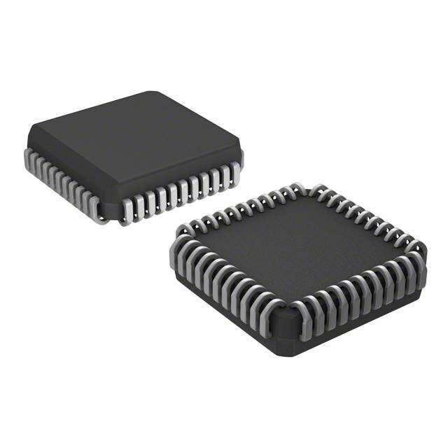
| 产品图片 |
|
| rohs | 符合RoHS无铅 / 符合限制有害物质指令(RoHS)规范要求 |
| 产品系列 | 数据转换器IC,模数转换器 - ADC,Intersil ICL7106CM44Z- |
| 数据手册 | |
| 产品型号 | ICL7106CM44Z |
| 产品目录页面 | |
| 产品种类 | 模数转换器 - ADC |
| 供应商器件封装 | 44-MQFP(10x10) |
| 信噪比 | No |
| 分辨率 | 3 1/2 Digit |
| 包装 | 托盘 |
| 商标 | Intersil |
| 安装类型 | 表面贴装 |
| 封装 | Tray |
| 封装/外壳 | 44-QFP |
| 封装/箱体 | MQFP |
| 工作温度 | 0°C ~ 70°C |
| 工作电源电压 | 9 V |
| 工厂包装数量 | 96 |
| 接口 | - |
| 接口类型 | LCD |
| 数字或字符 | A/D,3.5 位数字 |
| 显示类型 | LCD |
| 最大工作温度 | + 70 C |
| 最小工作温度 | 0 C |
| 标准包装 | 96 |
| 电压-电源 | 4.75 V ~ 5.25 V |
| 电压参考 | Internal, External |
| 电流-电源 | - |
| 系列 | ICL7106 |
| 结构 | Dual-Slope |
| 转换器数量 | 1 |
| 转换速率 | 3 S/s |
| 输入类型 | Differential |
| 通道数量 | 1 Channel |
| 配置 | 7 段显示 |


- 商务部:美国ITC正式对集成电路等产品启动337调查
- 曝三星4nm工艺存在良率问题 高通将骁龙8 Gen1或转产台积电
- 太阳诱电将投资9.5亿元在常州建新厂生产MLCC 预计2023年完工
- 英特尔发布欧洲新工厂建设计划 深化IDM 2.0 战略
- 台积电先进制程称霸业界 有大客户加持明年业绩稳了
- 达到5530亿美元!SIA预计今年全球半导体销售额将创下新高
- 英特尔拟将自动驾驶子公司Mobileye上市 估值或超500亿美元
- 三星加码芯片和SET,合并消费电子和移动部门,撤换高东真等 CEO
- 三星电子宣布重大人事变动 还合并消费电子和移动部门
- 海关总署:前11个月进口集成电路产品价值2.52万亿元 增长14.8%


PDF Datasheet 数据手册内容提取
DATASHEET ICL7106, ICL7107, ICL7107S FN3082 31/2 Digit, LCD/LED Display, A/D Converters Rev 9.00 October 24, 2014 The Intersil ICL7106 and ICL7107 are high performance, low Features power, 31/2 digit A/D converters. Included are seven segment decoders, display drivers, a reference, and a clock. The • Guaranteed zero reading for 0V input on all scales ICL7106 is designed to interface with a liquid crystal display • True polarity at zero for precise null detection (LCD) and includes a multiplexed backplane drive; the ICL7107 • 1pA typical input current will directly drive an instrument size light emitting diode (LED) display. • True differential input and reference, direct display drive - LCD ICL7106, LED lCL7107 The ICL7106 and ICL7107 bring together a combination of high accuracy, versatility, and true economy. It features • Low noise - less than 15µVP-P autozero to less than 10µV, zero drift of less than 1µV/°C, • On-chip clock and reference input bias current of 10pA (max) and rollover error of less than one count. True differential inputs and reference are useful in • Low power dissipation - typically less than 10mW all systems, but give the designer an uncommon advantage • No additional active circuits required when measuring load cells, strain gauges and other bridge • Enhanced display stability type transducers. Finally, the true economy of single power supply operation (ICL7106), enables a high performance panel • Pb-free (RoHS compliant) meter to be built with the addition of only 10 passive components and a display. Ordering Information PART NUMBER TEMP. RANGE PACKAGE (Note2) PART MARKING (°C) (Pb-Free) PKG. DWG. # ICL7106CPLZ ICL7106CPLZ 0 to 70 40 Ld PDIP (Note3) E40.6 ICL7106CM44Z (Note4) ICL7106 CM44Z 0 to 70 44 Ld MQFP Q44.10x10 ICL7106CM44ZT (Notes4, 5) ICL7106 CM44Z 0 to 70 44 Ld MQFP Tape and Reel Q44.10x10 ICL7107CPLZ ICL7107CPLZ 0 to 70 40 Ld PDIP (Note3) E40.6 ICL7107SCPLZ ICL7107SCPLZ 0 to 70 40 Ld PDIP (Notes1, 3) E40.6 ICL7107CM44Z (Note4) ICL7107 CM44Z 0 to 70 44 Ld MQFP Q44.10x10 ICL7107CM44ZT (Notes4, 5) ICL7107 CM44Z 0 to 70 44 Ld MQFP Tape and Reel Q44.10x10 NOTES: 1. “S” indicates enhanced stability. 2. These Intersil Pb-free plastic packaged products employ special Pb-free material sets, molding compounds/die attach materials, and 100% matte tin plate plus anneal (e3 termination finish, which is RoHS compliant and compatible with both SnPb and Pb-free soldering operations). Intersil Pb-free products are MSL classified at Pb-free peak reflow temperatures that meet or exceed the Pb-free requirements of IPC/JEDEC J STD-020. 3. Pb-free PDIPs can be used for through hole wave solder processing only. They are not intended for use in Reflow solder processing applications. 4. For Moisture Sensitivity Level (MSL), please see product information page for ICL7106, ICL7107, ICL7107S. For more information on MSL, please see tech brief TB363. 5. Please refer to TB347 for details on reel specifications. FN3082 Rev 9.00 Page 1 of 17 October 24, 2014
ICL7106, ICL7107, ICL7107S Pin Configurations ICL7106, ICL7107, ICL7107S (PDIP) ICL7106, ICL7107 (MQFP) TOP VIEW TOP VIEW N DCV+11 123 433098 OOOSSSCCC 123 REF HI REF LO C+REF C-REF COMMO IN HI IN LO A-Z BUFF INT V- B1 4 37 TEST (1’s) A1 5 36 REF HI F1 6 35 REF LO 44 43 42 41 40 39 38 37 36 3534 NC 1 33 NC G1 7 34 CREF+ NC 2 32 G2 E1 8 33 CREF- TEST 3 31 C3 D2 9 32 COMMON OSC 3 4 30 A3 C2 10 31 IN HI NC 5 29 G3 B2 11 30 IN LO (10’s) A2 12 29 A-Z OSC 2 6 28 BP/GND F2 13 28 BUFF OSC 1 7 27 POL E2 14 27 INT V+ 8 26 AB4 D3 15 26 V- D1 9 25 E3 B3 16 25 G2 (10’s) C1 10 24 F3 (100’s) F3 17 24 C3 B1 1112 13 14 15 16 17 18 19 20 212223 B3 E3 18 23 A3 (100’s) (1000) AB4 19 22 G3 POL 20 21 BP/GND (MINUS) A1 F1 G1 E1 D2C2 B2 A2F2 E2 D3 FN3082 Rev 9.00 Page 2 of 17 October 24, 2014
ICL7106, ICL7107, ICL7107S Absolute Maximum Ratings Thermal Information Supply Voltage Thermal Resistance (Typical) JA (oC/W) ICL7106, V+ to V- . . . . . . . . . . . . . . . . . . . . . . . . . . . . . . . . . . . . . . . . . . 15V PDIP Package (Note7) . . . . . . . . . . . . . . . . . . . . . . . . . . 50 ICL7107, V+ to GND. . . . . . . . . . . . . . . . . . . . . . . . . . . . . . . . . . . . . . . . . 6V MQFP Package (Note7) . . . . . . . . . . . . . . . . . . . . . . . . . 75 ICL7107, V- to GND. . . . . . . . . . . . . . . . . . . . . . . . . . . . . . . . . . . . . . . . . .-9V Maximum Junction Temperature . . . . . . . . . . . . . . . . . . . . . . . . . . . .+150°C Analog Input Voltage (Either Input) (Note6). . . . . . . . . . . . . . . . . . . V+ to V- Maximum Storage Temperature Range . . . . . . . . . . . . . .-65°C to +150°C Reference Input Voltage (Either Input). . . . . . . . . . . . . . . . . . . . . . . . V+ to V- Pb-Free Reflow Profile (MQFP Package only). . . . . . . . . . . . . . . see TB493 Clock Input ICL7106. . . . . . . . . . . . . . . . . . . . . . . . . . . . . . . . . . . . . . . . . . . . TEST to V+ NOTE: Pb-free PDIPs can be used for through hole wave solder processing ICL7107. . . . . . . . . . . . . . . . . . . . . . . . . . . . . . . . . . . . . . . . . . . . .GND to V+ only. They are not intended for use in Reflow solder processing applications. Operating Conditions Temperature Range. . . . . . . . . . . . . . . . . . . . . . . . . . . . . . . . . 0°C to +70°C CAUTION: Do not operate at or near the maximum ratings listed for extended periods of time. Exposure to such conditions may adversely impact product reliability and result in failures not covered by warranty. NOTES: 6. Input voltages may exceed the supply voltages provided the input current is limited to ±100µA. 7. JA is measured with the component mounted on a low effective thermal conductivity test board in free air. See Tech Brief TB379 for details. Electrical Specifications (Note8) PARAMETER TEST CONDITIONS MIN TYP MAX UNIT SYSTEM PERFORMANCE Zero Input Reading VIN = 0.0V, full scale = 200mV -000.0 000.0 +000.0 Digital Reading Stability (Last Digit) (ICL7107S Only) Fixed input voltage (Note11) -000.0 000.0 +000.0 Digital Reading Ratiometric Reading VlN = VREF, VREF = 100mV 999 999/1000 1000 Digital Reading Rollover Error -VIN = +VlN 200mV - ±0.2 ±1 Counts Difference in reading for equal positive and negative inputs near full scale Linearity Full scale = 200mV or full scale = 2V maximum deviation - ±0.2 ±1 Counts from best straight line fit (Note10) Common Mode Rejection Ratio VCM = 1V, VIN = 0V, full scale = 200mV (Note10) - 50 - µV/V Noise VIN = 0V, full scale = 200mV - 15 - µV (peak-to-peak value not exceeded 95% of time) Leakage Current Input VlN = 0 (Note10) - 1 10 pA Zero Reading Drift VlN = 0, 0°C to +70°C (Note10) - 0.2 1 µV/°C Scale Factor Temperature Coefficient VIN = 199mV, 0°C to +70°C, - 1 5 ppm/°C (ext. ref. 0ppm/×°C) (Note10) End Power Supply Character V+ Supply Current VIN = 0 (does not include LED current for ICL7107) - 1.0 1.8 mA End Power Supply Character V- Supply Current ICL7107 Only - 0.6 1.8 mA COMMON Pin Analog Common Voltage 25kΩ between common and positive supply (withrespect 2.4 3.0 3.2 V to + supply) Temperature Coefficient of Analog Common 25kΩ between common and positive supply (withrespect - 80 - ppm/°C to + supply) DISPLAY DRIVER ICL7106 ONLY Peak-to-Peak Segment Drive Voltage V+ = to V- = 9V (Note9) 4 5.5 6 V Peak-to-Peak Backplane Drive Voltage FN3082 Rev 9.00 Page 3 of 17 October 24, 2014
ICL7106, ICL7107, ICL7107S Electrical Specifications (Note8) (Continued) PARAMETER TEST CONDITIONS MIN TYP MAX UNIT DISPLAY DRIVER ICL7107 ONLY Segment Sinking Current V+ = 5V, segment voltage = 3V Except Pins AB4 and POL 5 8 - mA Pin AB4 Only 10 16 - mA Pin POL Only 4 7 - mA NOTES: 8. Unless otherwise noted, specifications apply to both the ICL7106 and ICL7107 at TA = +25°C, fCLOCK = 48kHz. ICL7106 is tested in the circuit of Figure1. ICL7107 is tested in the circuit of Figure2. 9. Back plane drive is in phase with segment drive for “off” segment, 180 degrees out of phase for “on” segment. Frequency is 20 times conversion rate. Average DC component is less than 50mV. 10. Limit is not production tested. The maximum was established via characterization and/or design simulations. 11. Sample tested. Typical Applications and Test Circuits + - 9V IN + - R1 R5 R3 C4 R4 C1 C5C2 R2 C3 DISPLAY C1 = 0.1µF 40 39 38 37 36 35 34 33 32 31 30 29 28 27 26 25 24 23 22 21 C2 = 0.47µF OSC 1 OSC 2 OSC 3 TEST REF HI REF LO C+REF C-REF COM IN HI IN LO A-Z BUFF INT V- G2 C3 A3 G3 BP CCC345 === 1000..20022pµµFFF ICL7106 R1 = 24kΩ R2 = 47kΩ V+ D1 C1 B1 A1 F1 G1 E1 D2 C2 B2 A2 F2 E2 D3 B3 F3 E3 AB4 POL RR34 == 110k0ΩkΩ 1 2 3 4 5 6 7 8 9 10 11 12 13 14 15 16 17 18 19 20 R5 = 1MΩ DISPLAY FIGURE 1. ICL7106 TEST CIRCUIT AND TYPICAL APPLICATION WITH LCD DISPLAY COMPONENTS SELECTED FOR 200mV FULL SCALE +5V + - -5V IN R1 R5 R3 C4 R4 C1 C5 C2R2 C3 DISPLAY C1 = 0.1µF 40 39 38 37 36 35 34 33 32 31 30 29 28 27 26 25 24 23 22 21 C2 = 0.47µF OSC 1 OSC 2 OSC 3 TEST REF HI REF LO C+REF C-REF COM IN HI IN LO A-Z BUFF INT V- G2 C3 A3 G3 GND CCC345 === 1000..20022pµµFFF ICL7107 R1 = 24kΩ R2 = 47kΩ V+ D1 C1 B1 A1 F1 G1 E1 D2 C2 B2 A2 F2 E2 D3 B3 F3 E3 AB4 POL RR34 == 110k0ΩkΩ 1 2 3 4 5 6 7 8 9 10 11 12 13 14 15 16 17 18 19 20 R5 = 1MΩ DISPLAY FIGURE 2. ICL7107 TEST CIRCUIT AND TYPICAL APPLICATION WITH LED DISPLAY COMPONENTS SELECTED FOR 200mV FULL SCALE FN3082 Rev 9.00 Page 4 of 17 October 24, 2014
ICL7106, ICL7107, ICL7107S Design Information Summary Sheet • OSCILLATOR FREQUENCY • DISPLAY COUNT fOSC = 0.45/RC VIN COUNT = 1000--------------- COSC > 50pF; ROSC > 50kΩ VREF fOSC (Typ) = 48kHz • CONVERSION CYCLE • OSCILLATOR PERIOD tCYC = tCL0CK x 4000 tOSC = RC/0.45 tCYC = tOSC x 16,000 • INTEGRATION CLOCK FREQUENCY when fOSC = 48kHz; tCYC = 333ms fCLOCK = fOSC/4 • COMMON MODE INPUT VOLTAGE • INTEGRATION PERIOD (V- + 1V) < VlN < (V+ - 0.5V) tINT = 1000 x (4/fOSC) • AUTO-ZERO CAPACITOR • 60/50Hz REJECTION CRITERION 0.01µF < CAZ < 1µF tINT/t60Hz or tlNT/t60Hz = Integer • REFERENCE CAPACITOR • OPTIMUM INTEGRATION CURRENT 0.1µF < CREF < 1µF IINT = 4µA • VCOM Biased between Vi and V-. • FULL SCALE ANALOG INPUT VOLTAGE VlNFS (Typ) = 200mV or 2V • VCOM V+ - 2.8V Regulation lost when V+ to V- < 6.8V • INTEGRATE RESISTOR V If VCOM is externally pulled down to (V+ to V-)/2, R = -----I--N----F---S--- the VCOM circuit will turn off. INT I INT • ICL7106 POWER SUPPLY: SINGLE 9V • INTEGRATE CAPACITOR V+ - V- = 9V t I INT INT Digital supply is generated internally C = -------------------------------- INT VINT VGND V+ - 4.5V • INTEGRATOR OUTPUT VOLTAGE SWING • ICL7106 DISPLAY: LCD t I INT INT Type: Direct drive with digital logic supply amplitude. V = -------------------------------- INT C INT • ICL7107 POWER SUPPLY: DUAL ±5.0V • VINT MAXIMUM SWING: V+ = +5V to GND (V- + 0.5V) < VINT < (V+ - 0.5V), VINT (Typ) = 2V V- = -5V to GND Digital Logic and LED driver supply V+ to GND • ICL7107 DISPLAY: LED Type: Nonmultiplexed Common Anode Typical Integrator Amplifier Output Waveform (INT Pin) AUTO ZERO PHASE SIGNAL INTEGRATE DEINTEGRATE PHASE (COUNTS) PHASE FIXED 0 - 1999 COUNTS 2999 - 1000 1000 COUNTS TOTAL CONVERSION TIME = 4000 x tCLOCK = 16,000 x tOSC FN3082 Rev 9.00 Page 5 of 17 October 24, 2014
ICL7106, ICL7107, ICL7107S Detailed Description to return to zero. The time required for the output to return to zero is proportional to the input signal. Specifically the digital reading Analog Section displayed is: Figure3 shows the analog section for the ICL7106 and ICL7107. DISPLAYCOUNT=1000---V-----I-N------ (EQ. 1) Each measurement cycle is divided into three phases. They are VREF (1) auto-zero (A-Z), (2) signal integrate (INT) and (3) deintegrate (DE). Differential Input Auto-Zero Phase The input can accept differential voltages anywhere within the common mode range of the input amplifier, or specifically from During auto-zero three things happen. First, input high and low are 0.5V below the positive supply to 1V above the negative supply. In disconnected from the pins and internally shorted to analog this range, the system has a CMRR of 86dB typical. However, care COMMON. Second, the reference capacitor is charged to the must be exercised to assure the integrator output does not reference voltage. Third, a feedback loop is closed around the saturate. A worst case condition would be a large positive common system to charge the auto-zero capacitor CAZ to compensate for mode voltage with a near full scale negative differential input offset voltages in the buffer amplifier, integrator, and comparator. voltage. The negative input signal drives the integrator positive Since the comparator is included in the loop, the A-Z accuracy is when most of its swing has been used up by the positive common limited only by the noise of the system. In any case, the offset mode voltage. For these critical applications the integrator output referred to the input is less than 10µV. swing can be reduced to less than the recommended 2V full scale Signal Integrate Phase swing with little loss of accuracy. The integrator output can swing to within 0.3V of either supply without loss of linearity. During signal integrate, the auto-zero loop is opened, the internal short is removed, and the internal input high and low are connected Differential Reference to the external pins. The converter then integrates the differential The reference voltage can be generated anywhere within the power voltage between IN HI and IN LO for a fixed time. This differential supply voltage of the converter. The main source of common mode voltage can be within a wide common mode range: up to 1V from error is a roll-over voltage caused by the reference capacitor losing or either supply. If, on the other hand, the input signal has no return gaining charge to stray capacity on its nodes. If there is a large with respect to the converter power supply, IN LO can be tied to common mode voltage, the reference capacitor can gain charge analog COMMON to establish the correct common mode voltage. At (increase voltage) when called up to deintegrate a positive signal but the end of this phase, the polarity of the integrated signal is lose charge (decrease voltage) when called up to deintegrate a determined. negative input signal. This difference in reference for positive or Deintegrate Phase negative input voltage will give a roll-over error. However, by selecting the reference capacitor such that it is large enough in The final phase is deintegrate, or reference integrate. Input low is comparison to the stray capacitance, this error can be held to less internally connected to analog COMMON and input high is than 0.5 count worst case. (see “Component Value Selection” on connected across the previously charged reference capacitor. page10.) Circuitry within the chip ensures that the capacitor will be connected with the correct polarity to cause the integrator output STRAY STRAY CREF RINT CAZ CINT CREF+ REF HI REF LO CREF- BUFFER V+ A-Z INT V+ 34 36 35 33 28 1 29 27 INTEGRATOR A-Z A-Z TO 10A - +- +- DIGITAL 31 + 2.8V SECTION IN HI INT DE- DE+ INPUT 6.2V A-Z HIGH A-Z COMPARATOR - N + DE+ DE- 32 COMMON INT A-Z AND DE(±) INPUT 30 LOW IN LO V- FIGURE 3. ANALOG SECTION OF ICL7106 AND ICL7107 FN3082 Rev 9.00 Page 6 of 17 October 24, 2014
ICL7106, ICL7107, ICL7107S Analog COMMON V+ This pin is included primarily to set the common mode voltage for battery operation (ICL7106) or for any system where the input V signals are floating with respect to the power supply. The REF HI COMMON pin sets a voltage that is approximately 2.8V more REF LO 6.8V negative than the positive supply. This is selected to give a ZENER minimum end-of-life battery voltage of about 6V. However, analog COMMON has some of the attributes of a reference ICL7106 IZ voltage. When the total supply voltage is large enough to cause ICL7107 the zener to regulate (>7V), the COMMON voltage will have a low voltage coefficient (0.001%/V), low output impedance (15Ω), and a temperature coefficient typically less than 80ppm/×°C. V- The limitations of the on chip reference should also be recognized, FIGURE 4A. however. With the ICL7107, the internal heating which results from the LED drivers can cause some degradation in performance. Due V+ to their higher thermal resistance, plastic parts are poorer in this respect than ceramic. The combination of reference Temperature V 6.8kΩ Coefficient (TC), internal chip dissipation, and package thermal ICL7106 20kΩ resistance can increase noise near full scale from 25µV to ICL7107 80µVP-P. Also the linearity in going from a high dissipation count such as 1000 (20 segments on) to a low dissipation count such as REF HI ICL8069 1111(8 segments on) can suffer by a count or more. Devices with 1.2V a positive TC reference may require several counts to pull out of an REF LO REFERENCE over-range condition. This is because over-range is a low COMMON dissipation mode, with the three least significant digits blanked. Similarly, units with a negative TC may cycle between overrange FIGURE 4B. and a non-overrange count as the die alternately heats and cools. All these problems are of course eliminated if an external FIGURE 4. USING AN EXTERNAL REFERENCE reference is used. TEST The ICL7106, with its negligible dissipation, suffers from none of these problems. In either case, an external reference can easily The TEST pin serves two functions. On the ICL7106 it is coupled be added, as shown in Figure4. to the internally generated digital supply through a 500Ω resistor. Thus, it can be used as the negative supply for externally Analog COMMON is also used as the input low return during generated segment drivers such as decimal points or any other auto-zero and deintegrate. If IN LO is different from analog presentation the user may want to include on the LCD display. COMMON, a common mode voltage exists in the system and is Figures5 and 6 show such an application. No more than a 1mA taken care of by the excellent CMRR of the converter. However, in load should be applied. some applications IN LO will be set at a fixed known voltage (power supply common for instance). In this application, analog COMMON should be tied to the same point, thus removing the common mode voltage from the converter. The same holds true V+ 1MΩ for the reference voltage. If reference can be conveniently tied to analog COMMON, it should be since this removes the common TO LCD DECIMAL mode voltage from the reference system. POINT ICL7106 Within the lC, analog COMMON is tied to an N-Channel FET that can sink approximately 30mA of current to hold the voltage 2.8V BP 21 below the positive supply (when a load is trying to pull the TEST common line positive). However, there is only 10µA of source 37 TO LCD current, so COMMON may easily be tied to a more negative BACKPLANE voltage thus overriding the internal reference. FIGURE 5. SIMPLE INVERTER FOR FIXED DECIMAL POINT The second function is a “lamp test”. When TEST is pulled high (to V+) all segments will be turned on and the display should read “1888”. The TEST pin will sink about 15mA under these conditions. CAUTION: In the lamp test mode, the segments have a constant DC voltage (no square-wave). This may burn the LCD display if maintained for extended periods. FN3082 Rev 9.00 Page 7 of 17 October 24, 2014
ICL7106, ICL7107, ICL7107S Digital Section V+ V+ Figures7 and 8 show the digital section for the ICL7106 and BP ICL7107, respectively. In the ICL7106, an internal digital ground is generated from a 6V Zener diode and a large P-Channel source TO LCD follower. This supply is made stiff to absorb the relatively large ICL7106 DECIMAL DECIMAL capacitive currents when the back plane (BP) voltage is switched. POINT POINTS SELECT The BP frequency is the clock frequency divided by 800. For three readings/sec., this is a 60Hz square wave with a nominal TEST amplitude of 5V. The segments are driven at the same frequency CD4030 and amplitude and are in phase with BP when OFF, but out of phase when ON. In all cases negligible DC voltage exists across GND the segments. FIGURE 6. EXCLUSIVE ‘OR’ GATE FOR DECIMAL POINT DRIVE Figure8 is the Digital Section of the ICL7107. It is identical to the ICL7106 except that the regulated supply and back plane drive have been eliminated and the segment drive has been increased from 2mA to 8mA, typical for instrument size common anode LED displays. Since the 1000 output (pin 19) must sink current from two LED segments, it has twice the drive capability or 16mA. In both devices, the polarity indication is “on” for negative analog inputs. If IN LO and IN HI are reversed, this indication can be reversed also, if desired. a a a a f b f b f b g g g c e c e c e c b d d d BACKPLANE 21 LCD PHASE DRIVER 7 7 7 TYPICAL SEGMENT OUTPUT SEGMENT SEGMENT SEGMENT 200 V+ DECODE DECODE DECODE 0.5mA SEGMENT LATCH OUTPUT 2mA 1000’s 100’s 10’s 1’s COUNTER COUNTER COUNTER COUNTER INTERNAL DIGITAL GROUND TO SWITCH DRIVERS FROM COMPARATOR OUTPUT 1 V+ CLOCK † 4 LOGIC CONTROL 6.2V 500Ω † THREE INVERTERS INTERNAL 37 TEST ONE INVERTER SHOWN FOR CLARITY DIGITAL VTH = 1V GROUND 26 V- 40 39 38 OSC 1 OSC 2 OSC 3 FIGURE 7. ICL7106 DIGITAL SECTION FN3082 Rev 9.00 Page 8 of 17 October 24, 2014
ICL7106, ICL7107, ICL7107S a a a a f b f b f b g g g c e c e c e c b d d d 7 7 7 SEGMENT SEGMENT SEGMENT DECODE DECODE DECODE TYPICAL SEGMENT OUTPUT V+ LATCH 0.5mA TO 1000’s 100’s 10’s 1’s SEGMENT COUNTER COUNTER COUNTER COUNTER 8mA TO SWITCH DRIVERS DIGITAL GROUND FROM COMPARATOR OUTPUT 1 V+ V+ CLOCK TEST † 4 LOGIC CONTROL 37 500Ω † THREE INVERTERS DIGITAL ONE INVERTER SHOWN FOR CLARITY 27 GROUND 40 39 38 OSC 1 OSC 2 OSC 3 FIGURE 8. ICL7107 DIGITAL SECTION System Timing INTERNAL TO PART Figure9 shows the clocking arrangement used in the ICL7106 and ICL7107. Two basic clocking arrangements can be used: 4 CLOCK 1. Figure9A. An external oscillator connected to pin 40. 2. Figure9B. An R-C oscillator using all three pins. The oscillator frequency is divided by four before it clocks the 40 39 38 decade counters. It is then further divided to form the three convert-cycle phases. These are signal integrate (1000 counts), GND ICL7107 reference deintegrate (0 to 2000 counts) and auto-zero (1000 to TEST ICL7106 3000 counts). For signals less than full scale, auto-zero gets the FIGURE 9A. unused portion of reference de-integrate. This makes a complete measure cycle of 4,000 counts (16,000 clock pulses) independent of input voltage. For three readings/second, an INTERNAL TO PART oscillator frequency of 48kHz would be used. 4 CLOCK To achieve maximum rejection of 60Hz pickup, the signal integrate cycle should be a multiple of 60Hz. Oscillator frequencies of 240kHz, 120kHz, 80kHz, 60kHz, 48kHz, 40kHz, 331/3kHz, etc., should be selected. For 50Hz rejection, oscillator frequencies of 200kHz, 100kHz, 662/3kHz, 50kHz, 40kHz, etc., 40 39 38 would be suitable. Note that 40kHz (2.5 readings/second) will reject both 50Hz and 60Hz (also 400Hz and 440Hz). R C RC OSCILLATOR FIGURE 9B. FIGURE 9. CLOCK CIRCUITS FN3082 Rev 9.00 Page 9 of 17 October 24, 2014
ICL7106, ICL7107, ICL7107S Component Value Selection Reference Voltage The analog input required to generate full scale output (2000 Integrating Resistor counts) is: VlN = 2VREF. Thus, for the 200mV and 2V scale, VREF Both the buffer amplifier and the integrator have a class A output should equal 100mV and 1V, respectively. However, in many stage with 100µA of quiescent current. They can supply 4µA of applications where the A/D is connected to a transducer, there drive current with negligible nonlinearity. The integrating resistor will exist a scale factor other than unity between the input should be large enough to remain in this very linear region over voltage and the digital reading. For instance, in a weighing the input voltage range, but small enough that undue leakage system, the designer might like to have a full scale reading when requirements are not placed on the PC board. For 2V full scale, the voltage from the transducer is 0.662V. Instead of dividing the 470kΩ is near optimum and similarly a 47kΩ for a 200mV scale. input down to 200mV, the designer should use the input voltage directly and select VREF = 0.341V. Suitable values for integrating Integrating Capacitor resistor and capacitor would be 120kΩ and 0.22µF. This makes the system slightly quieter and also avoids a divider network on The integrating capacitor should be selected to give the maximum the input. The ICL7107 with ±5V supplies can accept input voltage swing that ensures tolerance buildup will not saturate the signals up to ±4V. Another advantage of this system occurs when integrator swing (approximately. 0.3V from either supply). In the ICL7106 or the ICL7107, when the analog COMMON is used as a a digital reading of zero is desired for VIN 0. Temperature and weighing systems with a variable fare are examples. This offset reference, a nominal +2V full scale integrator swing is fine. For reading can be conveniently generated by connecting the voltage the ICL7107 with +5V supplies and analog COMMON tied to transducer between IN HI and COMMON and the variable (or supply ground, a ±3.5V to +4V swing is nominal. For three fixed) offset voltage between COMMON and IN LO. readings/second (48kHz clock) nominal values for ClNT are 0.22µF and 0.10µF, respectively. Of course, if different oscillator ICL7107 Power Supplies frequencies are used, these values should be changed in inverse proportion to maintain the same output swing. The ICL7107 is designed to work from ±5V supplies. However, if a negative supply is not available, it can be generated from the An additional requirement of the integrating capacitor is that it clock output with 2 diodes, 2 capacitors, and an inexpensive lC. must have a low dielectric absorption to prevent roll-over errors. Figure10 shows this application. See the ICL7660 datasheet for While other types of capacitors are adequate for this application, an alternative. polypropylene capacitors give undetectable errors at reasonable cost. In fact, in selected applications no negative supply is required. The conditions to use a single +5V supply are: Auto-Zero Capacitor 1. The input signal can be referenced to the center of the The size of the auto-zero capacitor has some influence on the common mode range of the converter. noise of the system. For 200mV full scale where noise is very 2. The signal is less than ±1.5V. important, a 0.47µF capacitor is recommended. On the 2V scale, 3. An external reference is used. a 0.047µF capacitor increases the speed of recovery from overload and is adequate for noise on this scale. V+ Reference Capacitor CD4009 A 0.1µF capacitor gives good results in most applications. However, where a large common mode voltage exists (i.e., the V+ OSC 1 REF LO pin is not at analog COMMON) and a 200mV scale is 1N914 + used, a larger value is required to prevent rollover error. Generally OSC 2 1µF will hold the rollover error to 0.5 count in this instance. 10µF OSC 3 0.047 - Oscillator Components µF ICL7107 For all ranges of frequency a 100kΩ resistor is recommended and GND 1N914 the capacitor is selected as shown in Equation2: V- 0.45 f = -----------For48kHzClock(3Readings/sec), RC (EQ. 2) V- = 3.3V C = 100pF. FIGURE 10. GENERATING NEGATIVE SUPPLY FROM +5V FN3082 Rev 9.00 Page 10 of 17 October 24, 2014
ICL7106, ICL7107, ICL7107S Typical Applications Application Notes The ICL7106 and ICL7107 may be used in a wide variety of NOTE # DESCRIPTION configurations. The circuits which follow show some of the AN016 “Selecting A/D Converters” possibilities, and serve to illustrate the exceptional versatility of these A/D converters. AN017 “The Integrating A/D Converter” The following application notes contain very useful information AN018 “Do’s and Don’ts of Applying A/D Converters” on understanding and applying this part and are available from AN023 “Low Cost Digital Panel Meter Designs” Intersil Corporation. AN046 “Building a Battery-Operated Auto Ranging DVM with the ICL7106” AN052 “Tips for Using Single Chip 31/2 Digit A/D Converters” AN9609 “Overcoming Common Mode Range Issues When Using Intersil Integrating Converters” Typical Applications TO PIN 1 TO PIN 1 OSC 1 40 OSC 1 40 100kΩ 100kΩ OSC 2 39 OSC 2 39 OSC 3 38 SET VREF OSC 3 38 SET VREF TEST 37 100pF = 100mV TEST 37 100pF = 100mV REF HI 36 REF HI 36 REF LO 35 REF LO 35 +5V 1kΩ 22kΩ 1kΩ 22kΩ CREF 34 CREF 34 0.1µF 0.1µF CREF 33 CREF 33 COMMON 32 1MΩ + COMMON 32 1MΩ + IN HI 31 IN HI 31 0.01µF IN 0.01µF IN IN LO 30 IN LO 30 0.47µF - 0.47µF - A-Z 29 + A-Z 29 47kΩ 47kΩ BUFF 28 9V BUFF 28 - INT 27 INT 27 0.22µF 0.22µF V - 26 V - 26 -5V G2 25 G2 25 C3 24 C3 24 TO DISPLAY TO DISPLAY A3 23 A3 23 G3 22 G3 22 BP 21 TO BACKPLANE GND 21 Values shown are for 200mV full scale, 3 readings/sec., floating supply Values shown are for 200mV full scale, 3 readings/sec. IN LO may be voltage (9V battery). tied to either COMMON for inputs floating with respect to supplies, or GND for single ended inputs. (See discussion in “Analog COMMON” on page7.) FIGURE 11. ICL7106 USING THE INTERNAL REFERENCE FIGURE 12. ICL7107 USING THE INTERNAL REFERENCE FN3082 Rev 9.00 Page 11 of 17 October 24, 2014
ICL7106, ICL7107, ICL7107S Typical Applications (Continued) TO PIN 1 TO PIN 1 OSC 1 40 OSC 1 40 100kΩ 100kΩ OSC 2 39 OSC 2 39 OSC 3 38 SET VREF OSC 3 38 SET VREF TEST 37 100pF = 100mV TEST 37 100pF = 100mV REF HI 36 REF HI 36 REF LO 35 V + REF LO 35 +5V CREF 34 1kΩ 10kΩ 10kΩ CREF 34 1kΩ 100kΩ 0.1µF 0.1µF 6.8V CREF 33 1.2V (ICL8069) CREF 33 COMMON 32 1MΩ + COMMON 32 1MΩ + IN HI 31 IN HI 31 0.01µF IN 0.01µF IN IN LO 30 IN LO 30 0.47µF - 0.47µF - A-Z 29 A-Z 29 47kΩ 47kΩ BUFF 28 BUFF 28 INT 27 INT 27 V - 26 0.22µF V - V - 26 0.22µF -5V G2 25 G2 25 C3 24 C3 24 TO DISPLAY TO DISPLAY A3 23 A3 23 G3 22 G3 22 GND 21 GND 21 IN LO is tied to supply COMMON establishing the correct common mode Since low TC zeners have breakdown voltages ~ 6.8V, diode must be voltage. If COMMON is not shorted to GND, the input voltage may float with placed across the total supply (10V). As in the case of Figure12, IN LO respect to the power supply and COMMON acts as a pre-regulator for the may be tied to either COMMON or GND. reference. If COMMON is shorted to GND, the input is single ended (referred to supply GND) and the preregulator is overridden. FIGURE 13. ICL7107 WITH AN EXTERNAL BAND-GAP FIGURE 14. ICL7107 WITH ZENER DIODE REFERENCE REFERENCE (1.2V TYPE) TO PIN 1 TO PIN 1 OSC 1 40 OSC 1 40 100kΩ 100kΩ OSC 2 39 OSC 2 39 OSC 3 38 SET VREF OSC 3 38 SET VREF TEST 37 100pF = 1V TEST 37 100pF = 100mV REF HI 36 REF HI 36 REF LO 35 V+ REF LO 35 +5V 1kΩ 10kΩ 15kΩ CCRREEFF 3343 0.1µF 25kΩ 24kΩ CCRREEFF 3343 0.1µF 1.2V (ICL8069) COMMON 32 1MΩ + COMMON 32 1MΩ + IN HI 31 IN HI 31 0.01µF IN 0.01µF IN IN LO 30 IN LO 30 0.47µF - 0.047µF - A-Z 29 A-Z 29 47kΩ 470kΩ BUFF 28 BUFF 28 INT 27 INT 27 0.22µF 0.22µF V - 26 V - 26 V- G2 25 G2 25 C3 24 C3 24 TO DISPLAY TO DISPLAY A3 23 A3 23 G3 22 G3 22 GND 21 BP/GND 21 An external reference must be used in this application, since the voltage between V+ and V- is insufficient for correct operation of the internal reference. FIGURE 15. ICL7106 AND ICL7107: RECOMMENDED COMPONENT FIGURE 16. ICL7107 OPERATED FROM SINGLE +5V VALUES FOR 2V FULL SCALE FN3082 Rev 9.00 Page 12 of 17 October 24, 2014
ICL7106, ICL7107, ICL7107S Typical Applications (Continued) TO PIN 1 V+ TO PIN 1 OSC 1 40 OSC 1 40 100kΩ 100kΩ OSC 2 39 OSC 2 39 OSC 3 38 OSC 3 38 SCALE TEST 37 100pF TEST 37 100pF FACTOR ADJUST REF HI 36 REF HI 36 REF LO 35 REF LO 35 22kΩ 100kΩ 1MΩ CREF 34 CREF 34 0.1µF 0.1µF 100kΩ220kΩ CREF 33 CREF 33 COMMON 32 COMMON 32 IN HI 31 IN HI 31 ZERO SILICON NPN 0.01µF ADJUST MPS 3704 OR IN LO 30 IN LO 30 0.47µF 0.47µF SIMILAR A-Z 29 A-Z 29 47kΩ 47kΩ BUFF 28 BUFF 28 9V INT 27 INT 27 0.22µF 0.22µF V - 26 V - 26 G2 25 G2 25 C3 24 C3 24 TO DISPLAY TO DISPLAY A3 23 A3 23 G3 22 G3 22 GND 21 BP 21 TO BACKPLANE A silicon diode-connected transistor has a temperature coefficient of The resistor values within the bridge are determined by the desired about -2mV/°C. Calibration is achieved by placing the sensing sensitivity. transistor in ice water and adjusting the zeroing potentiometer for a 000.0 reading. The sensor should then be placed in boiling water and the scale-factor potentiometer adjusted for a 100.0 reading. FIGURE 17. ICL7107 MEASURING RATIOMETRIC VALUES OF QUAD FIGURE 18. ICL7106 USED AS A DIGITAL CENTIGRADE LOAD CELL THERMOMETER FN3082 Rev 9.00 Page 13 of 17 October 24, 2014
ICL7106, ICL7107, ICL7107S Typical Applications (Continued) V+ +5V 1 V+ OSC 1 40 1 V+ OSC 1 40 2 D1 OSC 2 39 2 D1 OSC 2 39 TO LOGIC 3 C1 OSC 3 38 3 C1 OSC 3 38 VCC 4 B1 TEST 37 4 B1 TEST 37 5 A1 REF HI 36 5 A1 REF HI 36 6 F1 REF LO 35 6 F1 REF LO 35 TO TO LOGIC 7 G1 CREF 34 LGONGDIC VCC 7 G1 CREF 34 8 E1 CREF 33 8 E1 CREF 33 9 D2 COMMON 32 12kΩ 9 D2 COMMON 32 10 C2 IN HI 31 The LM339 is required to 10 C2 IN HI 31 11 B2 IN LO 30 ensure logic compatibility 11 B2 IN LO 30 with heavy display loading. 12 A2 A-Z 29 12 A2 A-Z 29 13 F2 BUFF 28 LM339 13 F2 BUFF 28 14 E2 INT 27 14 E2 INT 27 +- 15 D3 V- 26 V- 15 D3 V- 26 V- 16 B3 G2 25 16 B3 G2 25 17 F3 C3 24 O/RANGE +- 17 F3 C3 24 O/RANGE 18 E3 A3 23 18 E3 A3 23 +- 19 AB4 G3 22 19 AB4 G3 22 20 POL BP 21 U/RANGE - 20 POL BP 21 U/RANGE CD4023 OR + 74C10 33kΩ CD4023 OR 74C10 CD4077 FIGURE 19. CIRCUIT FOR DEVELOPING UNDERRANGE AND FIGURE 20. CIRCUIT FOR DEVELOPING UNDERRANGE AND OVERRANGE SIGNAL FROM ICL7106 OUTPUTS OVERRANGE SIGNALS FROM ICL7107 OUTPUT TO PIN 1 OSC 1 40 100kΩ OSC 2 39 10µF SCALE FACTOR ADJUST OSC 3 38 (VREF = 100mV FOR AC TO RMS) 100pF CA3140 100kΩ TEST 37 5µF + REF HI 36 - AC IN REF LO 35 1N914 CREF 34 1kΩ 22kΩ 470kΩ 0.1µF 2.2MΩ CREF 33 COMMON 32 1µF 10kΩ 1µF 10kΩ 1µF IN HI 31 4.3kΩ IN LO 30 0.47µF 0.22µF A-Z 29 47kΩ + BUFF 28 10µF 9V 100pF INT 27 - (FOR OPTIMUM BANDWIDTH) 0.22µF V - 26 G2 25 C3 24 TO DISPLAY A3 23 G3 22 BP 21 TO BACKPLANE Test is used as a common-mode reference level to ensure compatibility with most op amps. FIGURE 21. AC TO DC CONVERTER WITH ICL7106 FN3082 Rev 9.00 Page 14 of 17 October 24, 2014
ICL7106, ICL7107, ICL7107S Typical Applications (Continued) +5V DM7407 LED SEGMENTS ICL7107 130Ω 130Ω 130Ω FIGURE 22. DISPLAY BUFFERING FOR INCREASED DRIVE CURRENT Revision History The revision history provided is for informational purposes only and is believed to be accurate, but not warranted. Please go to the web to make sure that you have the latest revision. DATE REVISION CHANGE October 24, 2014 FN3082.9 Updated to the newest template. Page1: Updated copyright area. Ordering Information table - removed all non Pb-free parts (all obsolete: ICL7106CPL, ICL7106CM44, ICL7107CPL, ICL7107RCPL, ICL7107RCPLZ, ICL7107SCPL, ICL7107CM44, ICL7107CM44T) and removed ICL7107RCPLZ(obsolete). Page2, Removed the PDIP pinout for the ICL7107R, as it is obsolete. Page4, Reworded Electrical Spec Note 9 (formerly note 5) from: "Not tested, guaranteed by design." to:"Limitisnot production tested. The maximum was established via characterization and/or design simulations." Page15, Added Revision History and About Intersil verbiage. About Intersil Intersil Corporation is a leading provider of innovative power management and precision analog solutions. The company's products address some of the largest markets within the industrial and infrastructure, mobile computing and high-end consumer markets. For the most updated datasheet, application notes, related documentation and related parts, please see the respective product information page found at www.intersil.com. You may report errors or suggestions for improving this datasheet by visiting www.intersil.com/ask. Reliability reports are also available from our website at www.intersil.com/support © Copyright Intersil Americas LLC 2002-2014. All Rights Reserved. All trademarks and registered trademarks are the property of their respective owners. For additional products, see www.intersil.com/en/products.html Intersil products are manufactured, assembled and tested utilizing ISO9001 quality systems as noted in the quality certifications found at www.intersil.com/en/support/qualandreliability.html Intersil products are sold by description only. Intersil may modify the circuit design and/or specifications of products at any time without notice, provided that such modification does not, in Intersil's sole judgment, affect the form, fit or function of the product. Accordingly, the reader is cautioned to verify that datasheets are current before placing orders. Information furnished by Intersil is believed to be accurate and reliable. However, no responsibility is assumed by Intersil or its subsidiaries for its use; nor for any infringements of patents or other rights of third parties which may result from its use. No license is granted by implication or otherwise under any patent or patent rights of Intersil or its subsidiaries. For information regarding Intersil Corporation and its products, see www.intersil.com FN3082 Rev 9.00 Page 15 of 17 October 24, 2014
ICL7106, ICL7107, ICL7107S Dual-In-Line Plastic Packages (PDIP) E40.6 (JEDEC MS-011-AC ISSUE B) N 40 LEAD DUAL-IN-LINE PLASTIC PACKAGE E1 INDEX INCHES MILLIMETERS AREA 1 2 3 N/2 SYMBOL MIN MAX MIN MAX NOTES -B- A - 0.250 - 6.35 4 -A- A1 0.015 - 0.39 - 4 D E BASE A2 0.125 0.195 3.18 4.95 - PLANE A2 -C- A B 0.014 0.022 0.356 0.558 - SEATING PLANE L CL B1 0.030 0.070 0.77 1.77 8 D1 D1 A1 eA C 0.008 0.015 0.204 0.381 - B1 e eC C D 1.980 2.095 50.3 53.2 5 B e D1 0.005 - 0.13 - 5 B 0.010 (0.25) M C A B S E 0.600 0.625 15.24 15.87 6 NOTES: E1 0.485 0.580 12.32 14.73 5 1. Controlling Dimensions: INCH. In case of conflict between English e 0.100 BSC 2.54 BSC - and Metric dimensions, the inch dimensions control. eA 0.600 BSC 15.24 BSC 6 2. Dimensioning and tolerancing per ANSI Y14.5M-1982. eB - 0.700 - 17.78 7 3. Symbols are defined in the “MO Series Symbol List” in Section 2.2 of Publication No. 95. L 0.115 0.200 2.93 5.08 4 4. Dimensions A, A1 and L are measured with the package seated in N 40 40 9 JEDEC seating plane gauge GS-3. Rev. 0 12/93 5. D, D1, and E1 dimensions do not include mold flash or protrusions. Mold flash or protrusions shall not exceed 0.010 inch (0.25mm). 6. E and eA are measured with the leads constrained to be per- pendicular to datum -C- . 7. eB and eC are measured at the lead tips with the leads uncon- strained. eC must be zero or greater. 8. B1 maximum dimensions do not include dambar protrusions. Dam- bar protrusions shall not exceed 0.010 inch (0.25mm). 9. N is the maximum number of terminal positions. 10. Corner leads (1, N, N/2 and N/2 + 1) for E8.3, E16.3, E18.3, E28.3, E42.6 will have a B1 dimension of 0.030 - 0.045 inch (0.76 - 1.14mm). FN3082 Rev 9.00 Page 16 of 17 October 24, 2014
ICL7106, ICL7107, ICL7107S Metric Plastic Quad Flatpack Packages (MQFP) D Q44.10x10 (JEDEC MS-022AB ISSUE B) D1 44 LEAD METRIC PLASTIC QUAD FLATPACK PACKAGE -D- INCHES MILLIMETERS SYMBOL MIN MAX MIN MAX NOTES A - 0.096 - 2.45 - A1 0.004 0.010 0.10 0.25 - A2 0.077 0.083 1.95 2.10 - -A- -B- b 0.012 0.018 0.30 0.45 6 E E1 b1 0.012 0.016 0.30 0.40 - D 0.515 0.524 13.08 13.32 3 D1 0.389 0.399 9.88 10.12 4, 5 E 0.516 0.523 13.10 13.30 3 E1 0.390 0.398 9.90 10.10 4, 5 e L 0.029 0.040 0.73 1.03 - N 44 44 7 PIN 1 e 0.032 BSC 0.80 BSC - -H- A SPELAATNINEG Rev. 2 4/99 NOTES: 1. Controlling dimension: MILLIMETER. Converted inch 0.076 0.003 dimensions are not necessarily exact. 12o-16o -C- 2. All dimensions and tolerances per ANSI Y14.5M-1982. 0.40 0.20 0.016MIN 0.008 M C A-B S D S 3. Dimensions D and E to be determined at seating plane -C- . 0o MIN 4. Dimensions D1 and E1 to be determined at datum plane b -H- . A2 A1 0o-7o b1 5. Dimensions D1 and E1 do not include mold protrusion. Allowable protrusion is 0.25mm (0.010 inch) per side. 0.13/0.17 6. Dimension b does not include dambar protrusion. Allowable 12o-16o 0.005/0.007 dambar protrusion shall be 0.08mm (0.003 inch) total. L 7. “N” is the number of terminal positions. BASE METAL WITH PLATING 0.13/0.23 0.005/0.009 © Copyright Intersil Americas LLC 2002-2014. All Rights Reserved. All trademarks and registered trademarks are the property of their respective owners. For additional products, see www.intersil.com/en/products.html Intersil products are manufactured, assembled and tested utilizing ISO9001 quality systems as noted in the quality certifications found at www.intersil.com/en/support/qualandreliability.html Intersil products are sold by description only. Intersil may modify the circuit design and/or specifications of products at any time without notice, provided that such modification does not, in Intersil's sole judgment, affect the form, fit or function of the product. Accordingly, the reader is cautioned to verify that datasheets are current before placing orders. Information furnished by Intersil is believed to be accurate and reliable. However, no responsibility is assumed by Intersil or its subsidiaries for its use; nor for any infringements of patents or other rights of third parties which may result from its use. No license is granted by implication or otherwise under any patent or patent rights of Intersil or its subsidiaries. For information regarding Intersil Corporation and its products, see www.intersil.com FN3082 Rev 9.00 Page 17 of 17 October 24, 2014