ICGOO在线商城 > Labels, Signs, Barriers, Identification > Accessories > HW-USB-FLYLEADS-G
 Datasheet下载
- 型号: HW-USB-FLYLEADS-G
- 制造商: Xilinx
- 库位|库存: xxxx|xxxx
- 要求:
| 数量阶梯 | 香港交货 | 国内含税 |
| +xxxx | $xxxx | ¥xxxx |
查看当月历史价格
查看今年历史价格
HW-USB-FLYLEADS-G产品简介:
ICGOO电子元器件商城为您提供HW-USB-FLYLEADS-G由Xilinx设计生产,在icgoo商城现货销售,并且可以通过原厂、代理商等渠道进行代购。 HW-USB-FLYLEADS-G价格参考¥236.45-¥236.45。XilinxHW-USB-FLYLEADS-G封装/规格:Accessories, Xilinx FPGA, CPLDS, Platform Flash PROMs, XC18V00 PROMs, System ACE MPM - Cable Assembly。您可以下载HW-USB-FLYLEADS-G参考资料、Datasheet数据手册功能说明书,资料中有HW-USB-FLYLEADS-G 详细功能的应用电路图电压和使用方法及教程。
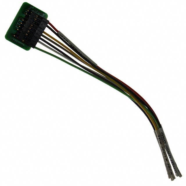
Xilinx Inc. 的 HW-USB-FLYLEADS-G 属于 Accessories(配件)类别,是一款用于 FPGA 开发调试的飞线式 USB 编程下载线缆。该产品主要作为 Xilinx 原装下载器(如 Platform Cable USB)的替代或扩展配件,适用于需要灵活连接的开发场景。

其典型应用场景包括:在原型验证平台、FPGA 开发板或定制 PCB 板上进行 JTAG 编程与调试。由于采用飞线设计(fly-leads),HW-USB-FLYLEADS-G 可直接通过导线连接目标板上的 JTAG 接口(TCK、TDI、TDO、TMS、GND),特别适用于标准接头不匹配、空间受限或需要非标布局的场合。它支持对 Xilinx 系列 FPGA 和 CPLD 器件进行配置烧录、逻辑分析仪(如 Vivado LabTools)连接及硬件调试。

该配件常配合 Vivado 或 ISE 设计套件使用,广泛应用于通信、工业控制、嵌入式视觉和科研教育等领域的开发与维护中。其优势在于连接灵活、兼容性强,适合工程师在实验室调试、现场维修或教学演示中快速实现设备编程与故障排查。使用时需注意引脚对应关系,避免接反导致损坏。
| 参数 | 数值 |
| 产品目录 | 编程器,开发系统 |
| 描述 | BOARD ADAPTER AND FLY LEADS |
| 产品分类 | |
| 品牌 | Xilinx Inc |
| 数据手册 | |
| 产品图片 |
|
| 产品型号 | HW-USB-FLYLEADS-G |
| rohs | 无铅 / 符合限制有害物质指令(RoHS)规范要求 |
| 产品系列 | - |
| 产品培训模块 | http://www.digikey.cn/PTM/IndividualPTM.page?site=cn&lang=zhs&ptm=16177 |
| 产品目录页面 | |
| 其它名称 | 122-1530 |
| 标准包装 | 1 |
| 特色产品 | http://www.digikey.cn/product-highlights/cn/zh/analog-devices-solutions-for-xilinx-fpgas/3178 |
| 配件类型 | USB 平台线缆 |
| 配套使用产品/相关产品 | Xilinx FPGA、CPLDS、平台闪存 PROM、XC18V00 PROM、系统 ACE MPM |


- 商务部:美国ITC正式对集成电路等产品启动337调查
- 曝三星4nm工艺存在良率问题 高通将骁龙8 Gen1或转产台积电
- 太阳诱电将投资9.5亿元在常州建新厂生产MLCC 预计2023年完工
- 英特尔发布欧洲新工厂建设计划 深化IDM 2.0 战略
- 台积电先进制程称霸业界 有大客户加持明年业绩稳了
- 达到5530亿美元!SIA预计今年全球半导体销售额将创下新高
- 英特尔拟将自动驾驶子公司Mobileye上市 估值或超500亿美元
- 三星加码芯片和SET,合并消费电子和移动部门,撤换高东真等 CEO
- 三星电子宣布重大人事变动 还合并消费电子和移动部门
- 海关总署:前11个月进口集成电路产品价值2.52万亿元 增长14.8%


PDF Datasheet 数据手册内容提取
0 R Platform Cable USB DS300 (v3.3) June 25, 2014 Product Specification 0 0 Features Platform Cable USB has these features: • Configures all Xilinx devices • Supported on Windows and Red Hat Enterprise Linux ♦ All Virtex® FPGA families • Automatically senses and adapts to target I/O voltage ♦ All Spartan® FPGA families • Interfaces to devices operating at 5V (TTL), 3.3V ♦ XC9500 / XC9500XL / XC9500XV CPLDs (LVCMOS), 2.5V, 1.8V, and 1.5V ♦ CoolRunner™ XPLA3 / CoolRunner-II CPLDs • LED Status Indicator ♦ XC18V00 ISP PROMs • CE, USB-IF, and FCC compliant ♦ Platform Flash XCF00S/XCF00P/XL PROMs • Intended for development — not recommended for ♦ XC4000 series FPGAs production programming • Programs serial peripheral interface (SPI) flash PROMs • Pb-free (RoHS-compliant) Platform Cable USB Description Platform Cable USB (Figure1) is a high-performance flying lead set is included for backward compatibility with download cable attaching to user hardware for the purpose of target systems that do not use the ribbon cable connector. programming or configuring any of the following Xilinx devices: Note: The next generation, Platform Cable USB II, is now available. • ISP Configuration PROMs Please refer to the DS593, Platform Cable USB II, for details. • CPLDs X-Ref Target - Figure 1 • FPGAs Platform Cable USB attaches to the USB port on a desktop or laptop PC with an off-the-shelf Hi-Speed USB A-B cable. It derives all operating power from the hub port controller. No external power supply is required. A sustained slave- serial FPGA configuration transfer rate of 24Mb/s is possible in a Hi-Speed USB environment. Actual transfer rates can vary if bandwidth of the hub is being shared with other USB peripheral devices. Device configuration and programming operations using DS300_01_011414 Platform Cable USB are supported by iMPACT download Figure 1: Xilinx Platform Cable USB software using Boundary-Scan (IEEE 1149.1 / IEEE 1532), slave-serial mode, or serial peripheral interface (SPI). Platform Cable USB supports indirect (via an FPGA IEEE 1149.1 [JTAG] port) programming of select flash memories including the Platform Flash XL configuration and storage device. Target clock speeds are selectable from 750kHz to 24MHz. Platform Cable USB attaches to target systems using a 14-conductor ribbon cable designed for high-bandwidth data transfers. An optional adapter that allows attachment of a © 2004–2014 Xilinx Inc. Xilinx, the Xilinx logo, Zynq, Virtex, Artix, Kintex, Spartan, ISE, Vivado and other designated brands included herein are trademarks of Xilinx in the United States and other countries. DS300 (v3.3) June 25, 2014 www.xilinx.com Product Specification 1
R Platform Cable USB Physical Description hubs, or external self-powered hubs), including legacy USB 1.1 hubs. However, performance is not optimal when The Platform Cable USB electronics are housed in a attached to USB 1.1 hubs (refer to "Hot Plug and Play," recyclable, fire-retardant plastic case (Figure2). An internal page5 for an explanation of USB enumeration). EMI shield attenuates internally generated emissions and Note: The DLC9G and legacy DLC9LP cable models draw less protects against susceptibility to radiated emissions. than 100mA from the host USB port. The legacy DLC9 cable model requires 230mA to operate in USB 2.0 Hi-Speed mode or X-Ref Target - Figure 2 150mA to operate in USB 2.0/1.1 full-speed mode. Some older RCooHmSpliant R CON2NmEmCTOR STATUS r1o0o0t mhuAb.s T ohre e lxetgearncya lD bLuCs-9p ocwabelree dm houdbesl dmoiegsh tn roet setrniuctm deervaitcee so nto Platform Cable USB SIGNALS Gnd hubs with the 100 mA restriction. Top View Model DLC9G JTA--G--orSeINriIaTl 2.10 Power 5V 0.07A T--D--I D--IN-- UHI-SSPEEBD Serial UHG -1 2 3 4 5 TTTVMDCreOSKfPDCROCVONLreGKEf Device Driver Installation CERTIFIED Made in U.S.A. 1.5 < Vref < 5.0 VDC A proprietary device driver is required to use Platform Cable All dimensions are in inches. USB. Xilinx ISE software releases and service packs 4.55 incorporate this device driver beginning with version 6.3.03i Side View for the Windows operating system or 7.1i for the Linux 0.65 operating system. Platform Cable USB is not recognized by 1.00 the operating system until an appropriate Xilinx ISE, ChipScope™ Pro or Platform Studio (EDK) software installation has been completed. ds300_02_011414 Refer to UG344, USB Cable Installation Guide, for a Figure 2: Plastic Case Physical Dimensions complete guide to installation of the Platform Cable USB and its device drivers. Operation Firmware Updates This section describes how to connect and use Platform Cable USB. Platform Cable USB is a RAM-based product. Application code is downloaded each time the cable is detected by the Minimum Host Computer Requirements host operating system. USB protocol guarantees that the code is successfully downloaded. The host computer must contain a USB Host Controller with one or more USB ports. The controller can reside on the PC All files necessary for successful cable communication are motherboard, or can be added using a PCI expansion card included with every Xilinx ISE software installation CD. or PCMCIA card. Revised application code is periodically distributed in subsequent software releases. ISE Service Pack and Platform Cable USB is supported on systems that meet the WebPACK™ releases can be downloaded from Xilinx ISE® system requirements. For environmental www.xilinx.com. Project Navigator automatically checks for details, go to: new releases when an Internet connection is detected. http://www.xilinx.com/products/design_resources/ When Xilinx applications are invoked and a connection is design_tool/index.htm established with Platform Cable USB, version information for several software components is displayed in a command log. and select the ISE tool of choice. Platform Cable USB is designed to take full advantage of the bandwidth of USB 2.0 Platform Cable USB also contains an embedded in-circuit ports, but it is also backward-compatible with USB 1.1 ports. programmable CPLD. Each time a Xilinx application is Refer to "Hub Types and Cable Performance," page16 for invoked, the firmware version for the CPLD is examined. additional information on connection environments and The CPLD is automatically reprogrammed over the cable if bandwidth. the firmware version is out of date (see Figure3). Although a rare event, when CPLD reprogramming is Operating Power necessary, the CPLD reprogramming process can take Platform Cable USB is a bus-powered device that draws considerable time and must not be interrupted once started. less than 100 mA from the host USB port under all The reprogramming time via a USB 2.0 port can typically operating conditions, automatically adapting to the take 10 to 15 minutes. Reprogramming time varies capabilities of the host USB port to achieve the highest depending on the ISE software version, the type of USB possible performance. port, and the performance of the host system. Later versions of the ISE software can reprogram CPLDs faster Platform Cable USB enumerates on any USB port type (for than older versions. example, USB ports on root hubs, external bus-powered DS300 (v3.3) June 25, 2014 www.xilinx.com Product Specification 2
R Platform Cable USB During a CPLD update, the Status LED illuminates red, and X-Ref Target - Figure 4 a progress bar indicates communication activity (see Figure4). CPLD updates should never be interrupted. When an update is complete, the Status LED returns to either amber or green, and the cable is ready for normal operation. X-Ref Target - Figure 3 DS300_04_110604 Figure 4: CPLD Update Progress Bar DS300_03_011414 Figure 3: CPLD Update Notification DS300 (v3.3) June 25, 2014 www.xilinx.com Product Specification 3
R Platform Cable USB Found New Hardware Wizard (for Windows Only) Platform Cable USB should be disconnected from the host system during the initial software installation. The first time a cable is attached after software installation, Windows invokes the Found New Hardware wizard and registers device drivers for the Platform Cable USB Firmware Loader (see Figure5) and for the Platform Cable USB itself (see Figure6). Windows invokes the Found New Hardware flow each time Platform Cable USB is plugged into a different physical USB port for the first time. The wizard screens could be slightly different for Windows 2000 environments. X-Ref Target - Figure 5 ds300_05_112904 Figure 5: a) Firmware Loader PID Detected; b) Firmware Loader Driver Registered X-Ref Target - Figure 6 ds300_06_112904 Figure 6: a) Application PID Detected; b) Application Driver Registered DS300 (v3.3) June 25, 2014 www.xilinx.com Product Specification 4
R Platform Cable USB Hot Plug and Play X-Ref Target - Figure 8 The cable can be attached and removed from the host computer without the need to power-down or reboot. There is a momentary delay after connecting the cable to an available port before the Status LED illuminates. This process is called enumeration. When Platform Cable USB completes the enumeration process on a Windows system, a "Programming cables" entry appears in the Windows Device Manager (see Figure7). To display Device Manager, right-click on My Computer, then select Properties → Hardware → Device Manager. DS300_08_110604 X-Ref Target - Figure 7 Figure 8: iMPACT Cable Selection Drop-Down Menu X-Ref Target - Figure 9 DS300_07_110604 Figure 7: Device Manager Cable Identification DS300_09_110604 Figure 9: iMPACT Cable Communication Setup Dialog iMPACT Configuration Cable Selection Configuration Clock Speed Platform Cable USB can be designated as the "active" configuration cable by following the auto-connect sequence The Platform Cable USB configuration clock for configuring devices that is displayed when first starting (TCK_CCLK_SCK) frequency is selectable. Table1 shows an iMPACT session. the complete set of available TCK_CCLK_SCK speed selections for high-power USB ports. Note: During the auto-connect sequence, iMPACT selects PC4 as the "active" cable if both PC4 and Platform Cable USB are Table 1: Speed Selection for High-Power Ports connected simultaneously. TCK_CCLK_SCK Selection Units Alternatively, the cable can be manually selected using Frequency the Output → Cable Setup option on the iMPACT toolbar 1 24 MHz (see Figure 8). 2 12 MHz When the Cable Communications Setup dialog box is 3 (default) 6 MHz displayed (Figure9), the Communication Mode radio 4 3 MHz button must be set to "Platform Cable USB." 5 1.5 MHz Before switching from the Boundary-Scan mode to the Slave 6 750 kHz Serial mode or vice versa, use Output → Cable Disconnect. After the mode switch is complete, reestablish the cable In slave-serial or SPI mode, the TCK_CCLK_SCK speed connection using the Output → Cable Setup dialog. can be set to any one of the available selections. By default, the TCK_CCLK_SCK speed is set to 6MHz. Users should If an iMPACT session is active when the cable is removed, take care to select a TCK_CCLK_SCK frequency that the Status bar immediately indicates "No Connection." matches the slave-serial clock (CCLK or SPI clock) specification of the target device. DS300 (v3.3) June 25, 2014 www.xilinx.com Product Specification 5
R Platform Cable USB In Boundary-Scan mode, iMPACT 7.1i (and later) queries CPLD version = 0004h the BSDL file of each device in a target Boundary-Scan Cable Connection Established chain to determine the maximum Boundary-Scan clock Note: The actual revision number can be expected to change (JTAG TCK) frequency. iMPACT 7.1i (and later) with new software releases. automatically restricts the available TCK_CCLK_SCK selections to frequencies that are less than or equal to the X-Ref Target - Figure 10 slowest device in the chain. By default, iMPACT 7.1i (or later) selects either 6MHz or the highest common frequency when any device in the Boundary-Scan chain is not capable of 6MHz operation. Table2 shows the maximum supported JTAG TCK frequency for a variety of Xilinx devices. See the device data sheet or BSDL file for maximum JTAG TCK specifications. Note: iMPACT versions earlier than 7.1i do not restrict the TCK_CCLK_SCK selections in Boundary-Scan mode. Full-Speed or Accordingly, users should take care to select a TCK_CCLK_SCK High-Speed frequency that matches the JTAG TCK specifications for the Connection slowest device in the target Boundary-Scan chain. Active Active Cable TCK_CCLK Identification Frequency Table 2: Maximum JTAG Clock Frequencies Command Log Text Display Maximum JTAG Device Family Units Clock Frequency DS300_10_111904 XC9500/XL/XV 10 MHz Figure 10: iMPACT Status Bar XPLA3 10 MHz Status Indicator CoolRunner-II 33 MHz Platform Cable USB uses a bi-color Status LED to indicate XC18V00 10 MHz the presence of target voltage. When the ribbon cable is XCF00S/XCF00P 15 MHz connected to a mating connector on the target system, the Virtex 33 MHz Status LED is illuminated as a function of the voltage present on pin 2 (V ). Virtex-II 33 MHz REF Virtex-IIPro 33 MHz Users must design their system hardware with pin 2 attached to a voltage plane that supplies the JTAG, SPI, or Virtex-4 33 MHz slave-serial pins on the target device(s). Some devices have Virtex-5 33 MHz separate power pins for this purpose (VAUX), while others Spartan 5 MHz have a common supply for both VCCIO and the JTAG pins Spartan-II 33 MHz (TCK, TMS, TDI, and TDO). Refer to the target device Data Sheet for details on slave-serial or JTAG pins. Spartan-3 33 MHz Spartan-3A 10 MHz The Status LED is amber (see Figure11) when any one or more of the following conditions exist: Spartan-3E 10 MHz • The ribbon cable is not connected to a target system A Status bar on the bottom edge of the iMPACT GUI • The target system is not powered provides useful information about operating conditions. If the host port is USB 1.1, Platform Cable USB connects at • The voltage on the V pin is < +1.5V REF full-speed, and the Status bar shows "usb-fs." If the host The Status LED is green when all of the following port is USB 2.0, Platform Cable USB connects at Hi-Speed conditions exist: and the Status bar shows "usb-hs." The active TCK_CCLK_SCK frequency is shown in the • The ribbon cable is connected to a target system lower right-hand corner of the Status bar (see Figure10). • The target system is powered The command log also includes information about • The voltage on the V pin is ≥ +1.5V REF communication with the cable. When the cable is selected The Status LED is Off whenever Platform Cable USB enters a using the Cable Communication Setup dialog box, the command log indicates: Suspend state, or is disconnected from a powered USB port. Firmware version = 1 CPLD file version = 0004h DS300 (v3.3) June 25, 2014 www.xilinx.com Product Specification 6
R Platform Cable USB X-Ref Target - Figure 11 X-Ref Target - Figure 12 Amber indicates no target voltage Green indicates target voltage present ds300_11a_011414 Figure 12: Suspend Warning When iMPACT Is Busy The target interface logic, including drivers for TCK_CCLK_SCK, TMS_PROG_SS, and TDI_DIN_MOSI, is not powered in the Suspend mode. These signals float to any DC bias level provided by the target hardware during Suspend. Note: Some computers remove power entirely from the USB port in Suspend mode. This is equivalent to a physical disconnect of the cable. When operation resumes, it is necessary to manually re- DS300_11_011414 establish a connection to the cable using the Output → Cable Figure 11: Status LEDs Indicating Target Voltage Setup toolbar selection. Suspend State Platform Cable USB Connections Every USB device, including Platform Cable USB, can be This section of the data sheet discusses physical placed into a Suspend state by the host operating system. connections from Platform Cable USB to the host PC and This can occur during any of the following usage scenarios: the target system. • The Suspend function key on a laptop computer is pressed. High-Performance Ribbon Cable • The display panel of a laptop is placed in the closed A 6" ribbon cable is supplied and recommended for position for transport while applications are running. connection to target systems (refer to Figure13). The cable • There is an extended period of time without data incorporates multiple signal-ground pairs and facilitates transfer activity on the cable when connected to a error-free connections. battery-powered laptop. To take advantage of the ribbon cable, a mating connector • There is an extended period of time without data transfer must be incorporated into the target system. This connector activity on the cable when connected to a desktop PC is normally installed only during prototype checkout. When configured with an "Energy Efficiency" option. the production hardware is functional and the ISP devices The purpose of the Suspend state is to reduce overall can be configured from alternate sources, the connector can power consumption. Suspend requests can be either global be eliminated as a cost reduction option. Maintaining the or port-specific. footprint for this connector is a wise choice if space permits. Platform Cable USB must consume less than 500µA from The connector is a 2mm shrouded keyed header. See the hub port when it enters the Suspend state. "Target Interface Connectors," page8 for vendor part Consequently, the Status LED is turned off and remains off numbers and pin assignments. until commanded to resume. If an iMPACT operation is in progress when Suspend is attempted, iMPACT displays a message indicating that Suspend is blocked until the operation is complete or is prematurely terminated (Figure12). DS300 (v3.3) June 25, 2014 www.xilinx.com Product Specification 7
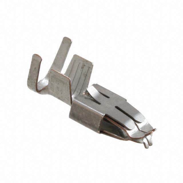
R Platform Cable USB X-Ref Target - Figure 13 Notes: 1. This method of connection is not recommended because it can result in poor signal integrity. Additionally, damage can result if the leads are unintentionally connected to high voltages. 2. One flying wire adapter with wires is supplied with the Platform Cable USB. Additional flying wire adapters with wires can be purchased separately (see "Ordering Information," page20). Physical Connection to the Host Each Platform Cable USB includes a detachable, Hi-Speed certified 1.8meter A-B cable (Figure16). Under no circumstances should user-supplied cables exceed 5meters. Sub-channel cables (intended for low-speed 1.5Mb/s signaling) should not be used with Platform Cable USB. A standard series B receptacle is incorporated into the left DS300_12_011414 side of the case for mating with the detachable Hi-Speed A-B Figure 13: High-Performance Ribbon Cable cable. A separate chassis ground is attached to the A-B cable drain wire and returns ESD current to the host system ground. Notes: 1. Ribbon Cable: 14 conductor, 1.0mm center, round conductor flat X-Ref Target - Figure 16 cable, 28 AWG (7x36) stranded conductors, gray PVC with pin 1 edge marked. 2. 2mm ribbon female polarized connector, IDC connection to ribbon. Contacts are beryllium copper plated, 30 micro-inches gold plating over 50 micro-inches nickel. The connectors mate to 0.5mm square posts on 2mm centers. 3. One ribbon cable is supplied with the Platform Cable USB. Additional ribbon cables can be purchased separately (see "Ordering Information," page20). Flying Wire Adapter An adapter is provided for attachment to legacy target systems that do not incorporate a shrouded male 2mm connector (Figure14). The adapter makes it possible to use ds300_15_110804 flying wires for connection to distributed terminals on a Figure 16: Standard A-B Host Interface target system. CableandSeriesBReceptacle The adapter is a small circuit board with two connectors (Figure15). The connector on the bottom side of the Target Interface Connectors adapter mates with the 14-pin Platform Cable USB male Mating connectors for attachment of the high-performance 2mm connector. A 7-pin right-angle header on the top ribbon cable to a target system are available in both side of the adapter mates with the standard Xilinx flying through-hole and surface mount configurations (Figure17). wire set (included). Shrouded and/or keyed versions should always be used to X-Ref Target - Figure 14 guarantee proper orientation when inserting the cable. The connector requires only 0.162in2 of board space. RCooHmSpliant Platform Cable USRB COSNIG2NmNEAmCLTSOR STATUS CERTIFIEDUHI-SSPEEBD MSMPaeoodrwedi aieenl rl U .DS5U.VLAH.C G 9 G- 1 0 2.0 73A 4 5 J1TTTTV.T5MDAC--r-- DeOG<--SK--fI VorrPDeCSfRO CeIV<DNONr-Lr i-II5eaGN-KET-.fl0 VGDnCd R JTAG | SERIAL VTTr-GeTC-D-fDNK O I D | | | | | I V N| C D rDI eTCGIOfNLNNKDE Tish ues teadrg aest say rsetfeemre vnocleta fgoer tahpep oliuetdp tuot pbiunf f2e rosf tthhaist dcorinven ethcteo r ADAPTER DS300_13_TM0S 8| PR1OG006 TDI_DIN_MOSI, TCK_CCLK_SCK, and TMS_PROG_SS pins.Table3 provides some third-party sources for mating Figure 14: Flying Wire Adapter (Top) with Wires connectors that are compatible with the Platform Cable USB ribbon cable. X-Ref Target - Figure 15 DS300_14_113004 Figure 15: Flying Wire Adapter (Side) w/o Wires DS300 (v3.3) June 25, 2014 www.xilinx.com Product Specification 8
R Platform Cable USB X-Ref Target - Figure 17 0.248" 0.299" SPI Slave Serial JTAG 0.0787" (2 mm) NC INIT NC 14 13 GND NC NC NC 12 11 GND MOSI DIN TDI 10 9 GND MISO DONE TDO 8 7 GND 0.472" 0.656" 0.0787" SCK CCLK TCK 6 5 GND TYP. SS PROG TMS 4 3 GND VREF VREF VREF 2 1 GND(1) 0.020" (0.5 mm) SQ. TYP. DS300_16_021507 Figure 17: Target Interface Connector DimensionsandSignalAssignments Table 3: Mating Connectors for 2mm Pitch, 14-Conductor Ribbon Cable SMT, Through-Hole, Through-Hole, Manufacturer(1) Web Site Vertical Vertical RightAngle Molex 87832-1420 87831-1420 87833-1420 www.molex.com FCI 98424-G52-14 98414-G06-14 98464-G61-14 www.fciconnect.com Comm Con Connectors 2475-14G2 2422-14G2 2401R-G2-14 www.commcon.com Notes: 1. Some manufacturer pin assignments do not conform to Xilinx pin assignments. Please refer to the manufacturer’s data sheet for more information. 2. Additional ribbon cables can be purchased separately from the Xilinx Online Store. DS300 (v3.3) June 25, 2014 www.xilinx.com Product Specification 9
R Platform Cable USB TDI_DIN_MOSI and TMS_PROG_SS Timing Specifications For JTAG, SPI, and slave-serial configuration modes, the where T is the TCK_CCLK_SCK Low time at 24MHz, CLK/2 TDI_DIN_MOSI and TMS_PROG_SS outputs change on and T is the maximum TDI_DIN_MOSI or CPD(MAX) falling edges of TCK_CCLK_SCK (Figure18). Target TMS_PROG_SS propagation delay relative to devices sample TDI_DIN_MOSI and TMS_PROG_SS on TCK_CCLK_SCK inherent in the output stage of the cable. rising edges of TCK_CCLK_SCK. The minimum setup time Reducing the TCK_CCLK_SCK frequency increases the T for target device sampling of TDI_DIN_MOSI or data setup time at the target. TTSU(MIN) TMS_PROG_SS is: Note: Timing specifications apply when VREF = 3.3V. Operation T = T – T at 24MHz might not be possible when using a VREF below 3.3V TTSU(MIN) CLK/2 CPD(MAX) due to the increased propagation delay through the output buffer = 20.83ns – 9.2ns stage of the cable. = 11.63ns X-Ref Target - Figure 18 TMS_PROG_SS Changes on Negative TDI_DIN_MOSI Changes Edge of TCK_CCLK_SCK (G1) on Negative Edge of TCK_CCLK_SCK (G2) DS300_17_021707 Figure 18: TDI_DIN_MOSI and TMS_PROG_SS Timing with Respect to TCK_CCLK_SCK TDO/MISO Timing Issues When read operations are being performed in Boundary-Scan example, Figure20 shows a 12ns TDO delay for an or SPI mode, there must be sufficient time during each one- XC2C256-VQ100 CPLD. half clock cycle for TDO/MISO to propagate back to the cable Finally, signal conditioning circuitry in Platform Cable USB for sampling. Figure19, Figure20, page11, and Figure21, introduces a third phase delay of approximately 12ns between page12 illustrate a potential problem when a 24MHz TDO_DONE_MISO and the logic that samples the signal. TCK_CCLK_SCK frequency is selected. An output buffer in Platform Cable USB introduces a phase delay of 4ns between Note: (Refer to Figure21, page12 for the TDO_DONE_MISO to the cable and the target. (See cursors C1 and C2 in Figure19, CBL_TDO delay.) page11 for the CBL_TCK to TCK_CCLK_SCK delay.) Data is sampled approximately 11ns after the rising edge of The target device has a variable propagation delay from the CBL_TCK. The total propagation delay must be carefully negative edge of TCK_CCLK_SCK to assertion of considered to successfully operate at 24MHz. Refer to TDO_DONE_MISO. (Refer to Figure20 for the Figure30, page19 for set-up timing requirements. TCK_CCLK_SCKtoTDO_DONE_MISO delay.) For DS300 (v3.3) June 25, 2014 www.xilinx.com Product Specification 10
R Platform Cable USB X-Ref Target - Figure 19 DS300_18_110204 Figure 19: TDO_DONE_MISO Timing with Respect to TCK_CCLK_SCK (CBL_TCK to TCK_CCLK_SCK Delay) X-Ref Target - Figure 20 DS300_19_110204 Figure 20: TDO_DONE_MISO Timing with Respect to TCK_CCLK_SCK (TCK_CCLK_SCK to TDO_DONE_MISO Delay) DS300 (v3.3) June 25, 2014 www.xilinx.com Product Specification 11
R Platform Cable USB X-Ref Target - Figure 21 DS300_20_110204 Figure 21: TDO_DONE_MISO Timing with Respect to TCK_CCLK_SCK (TDO_DONE_MISO to CBL_TDO Delay) Target Reference Voltage Sensing (V ) Table 4: Output Signal Level as a Function of the V REF REF Platform Cable USB incorporates an over-voltage clamp on VREF Voltage on Target Output Signal Status LED System (VDC) Levels (VDC) Color the V pin of the 2mm ribbon cable connector. The REF clamped voltage (V ) supplies a high-slew-rate buffer 3.30 ≤ V ≤ 5.00 ≅ 3.3 Green REF_A REF (NC7SZ125) that drives each of the three output signals. Notes: V must be a regulated voltage. REF 1. There are weak pull-up resistors to VREF_A on each of the three Note: Do not insert a current-limiting resistor in the target system output drivers (TCK_CCLK_SCK, TMS_PROG_SS, and TDI_DIN_MOSI). The output drivers are active only during between the VREF supply and pin 2 on the 2mm connector. configuration and programming operations. Between operations, No damage to Platform Cable USB occurs if the A-B cable the drivers are set to high-Z. is unplugged from the host while the ribbon cable or flying Xilinx applications actively drive the outputs to logic 1 before leads are attached to a powered target system. Similarly, no setting the respective buffer to high-Z, avoiding the damage to target systems occurs if Platform Cable USB is possibility of a slow rise-time transition caused by a charge powered and attached to the target system while the target path through the pull-up resistor into parasitic capacitance system power is off. on the target system. Buffers for the output signals (TCK_CCLK_SCK, TMS_PROG_SS, and TDI_DIN_MOSI) are set to high-Z Output Driver Structure when V drops below 1.40V. The output buffer amplitude REF linearly tracks voltage changes on the V pin when Platform Cable USB drives three target signals: REF 1.40V≤V ≤3.30V. Amplitude is clamped at TCK_CCLK_SCK, TMS_PROG_SS, and TDI_DIN_MOSI. REF approximately 3.30V when 3.30≤V ≤5.00V. Each of these signals incorporates the same driver REF topology. A Xilinx XC2C256 Coolrunner-II CPLD generates Refer to Table4 for the relationship between V voltage REF the output signals. and output signal amplitude. Each signal is routed to an external NC7SZ125 high-speed Table 4: Output Signal Level as a Function of the VREF CMOS buffer (Figure22). Series-damping resistors (30Ω) reduce reflections. Weak pull-up resistors (20kΩ) maintain V Voltage on Target Output Signal Status LED REF System (VDC) Levels (VDC) Color a defined logic level when the buffers are set to high-Z. The pull-up resistors terminate to V . 0.00 ≤ V < 1.40 High-Z Amber REF_A REF 1.40 ≤ V < 3.30 V Green REF REF DS300 (v3.3) June 25, 2014 www.xilinx.com Product Specification 12
R Platform Cable USB Signal Integrity X-Ref Target - Figure 22 VCC33_SW VREF_A Platform Cable USB uses high-slew-rate buffers to drive TCK_CCLK_SCK, TMS_PROG_SS, and TDI_DIN_MOSI. CPLD Each buffer has a 30Ω series termination resistor. Users should pay close attention to PCB layout to avoid VREF_A transmission line effects. Visit the Xilinx Signal Integrity 2 mm Connector Central website, and see specifically Xilinx Application Note I/O XFCE PIN XAPP361, Planning for High Speed XC9500XV Designs, for NC7SZ125 detailed signal integrity assistance. Internal High-Z Three-State If the target system has only one programmable device, the Control DS300_22_120904 2mm connector should be located as close as possible to Figure 22: Target Interface Driver Topology the target device. If there are multiple devices in a single chain on the target system, users should consider buffering TCK_CCLK_SCK. Differential driver/receiver pairs provide Refer to Figure23 to determine the expected value of excellent signal quality when the rules identified in V as a function of V . REF_A REF Figure25 are followed. Buffering is essential if target X-Ref Target - Figure 23 devices are distributed over a large PCB area. Each differential driver and/or receiver pair contributes approximately 5ns of propagation delay. This is insignificant when using 12MHz or slower clock speeds. Each differential receiver can drive multiple target devices if there are no branches on the PCB trace and the total trace length is less than four inches. A series termination resistor should be placed adjacent to the single-ended output of the differential receiver. X-Ref Target - Figure 25 Route A & B traces for each differential DS300_22_113004 SN65LVDS105 pair in parallel with equal length and Four Differential consistent spacing Figure 23: V as a Function of V REF_A REF Drivers SN65LVDS2 (2) Series Termination Resistor Input Receiver Structure TCK_CCLK 1 TCK_CCLK_1 Four A Schottky diode is used to protect the TDO_DONE_MISO Buffered voltage comparator (Figure24). In effect, Platform Cable Clocks 4 TCK_CCLK_4 USB looks for voltages below V MAX to detect logic 0, and IL tolerates voltages much higher than V because TDO REF_A could be terminated to a supply other than V . REF Locate one receiver adacent to each target device X-Ref Target - Figure 24 Locate driver package adjacent to 2mm connector VREF_A DS300_24_110804 CPLD Figure 25: Differential Clock Buffer Example VCC33 Note: If the target system incorporates a buffer for TCK_CCLK_SCK and the 24MHz clock rate is used, it is recommended that the same buffer type also be provided for LT1719 2 mm Connector TMS_PROG_SS. This maintains a consistent phase relationship I/O between TCK_CCLK_SCK and TMS_PROG_SS. A buffer is not XFCE PIN needed for TDI_DIN_MOSI, because it sees only one load. BAT54 DS300_23_120904 Figure 24: Target Interface Receiver Topology DS300 (v3.3) June 25, 2014 www.xilinx.com Product Specification 13
R Platform Cable USB Target System Connections Multiple devices can be cascaded when using either JTAG X-Ref Target - Figure 26 or slave-serial topology in target systems. Figure27, +3.3V +3.3V 2 mm page14 shows typical JTAG connections, and Figure28, Connector page15 shows an example of slave-serial routing. V 2 VCC REF The Platform Cable USB can connect directly to a single SPI Bus(3) SPI flash device. Figure26 shows example SPI flash MISO 8 Q W ‘1’ connections. Refer to XAPP951, Configuring Xilinx FPGAs ST Micro MOSI 10 D with SPI Serial Flash, for a detailed reference design M25Pxx(1) showing the cable connections for programming an FPGA SS 4 S Serial Flash bitstream into a SPI flash device. HOLD ‘1’ SCK 6 C The DONE pin on FPGAs can be programmed to be an open-drain or active driver. For cascaded slave-serial GND(2) X GND topologies, an external pull-up resistor should be used, and all devices should be programmed for open-drain operation. Notes: If the 2mm connector is located a significant distance from 1. The example shows pin names for an STMicrosystems M25Pxx serial flash the target device, it is best to buffer TCK_CCLK_SCK, at a device. SPI flash devices from other vendors can have different pin names and requirements. See the SPI flash data sheet for the equivalent pins and minimum. These diagrams are intended to represent the device requirements. logical relationship between Platform Cable USB and target 2. Attach the following 2 mm connector pins to digital ground: 1, 3, 5, 7, 9, 11, 13. devices. Refer to "Signal Integrity," page13 for additional 3. Typically, an FPGA and other slave SPI devices, which are not shown, are buffering and termination information. connected to the SPI bus. The other devices on the SPI bus must be disabled when the cable is connected to the 2 mm connector to avoid signal contention. When a Xilinx FPGA is connected to the SPI bus, the FPGA PROG_B pin can be held Low to ensure the FPGA pins are kept in a high-impedance state. DS300_30_011414 Figure 26: Example of SPI Topology X-Ref Target - Figure 27 2 mm Connector VCCAUX(1) VREF 2 TDO 8 ISP TDI 10 TDI TDO TDI FPGA TDO TDI CPLD TDO PROM TMS 4 TMS TCK TMS TCK TMS TCK TCK 6 GND(2) X Notes: 1. Example implies that VCCO, VCCJ, VCC_CONFIG and VCCAUX for various devices are set to the same voltage. See device data sheets for appropriate JTAG voltage-supply levels. 2. Attach the following 2 mm connector pins to digital ground: 1, 3, 5, 7, 9, 11, 13. DS300_26_031006 Figure 27: Example of JTAG Chain Topology DS300 (v3.3) June 25, 2014 www.xilinx.com Product Specification 14
R Platform Cable USB X-Ref Target - Figure 28 VCCAUX(2) 2 mm Connector Optional Pull-Up VCCAUX(2) VREF 2 DONE 8 PROG DONE PROG DONE PROG DONE PROG 4 DIN 10 DIN FPGA1 DOUT DIN FPGA2 DOUT DIN FPGAn DOUT INIT 14 VCCO INIT CCLK INIT CCLK INIT CCLK CCLK 6 GND(3) X Notes: 1. Set Mode pins (M2-M0) on each FPGA to Slave-serial mode when using the USB cable, so that CCLK is treated as an input. 2. VCCAUXis 3.3V for Virtex-II FPGAs, 2.5V for Virtex-II Pro FPGAs, or 2.5V for Spartan-3/3E FPGAs. The VCCAUX for Spartan-3A FPGAs can be 2.5V or 3.3V. Virtex-4/5 serial configuration pins are on a dedicated VCC_CONFIG (VCCO_0), 2.5V supply. Other FPGA families do not have a separate VCCAUX supply. 3. Attach the following 2 mm connector pins to digital ground: 1, 3, 5, 7, 9, 11, 13. DS300_25_021507 Figure 28: Example of Cascaded Slave-Serial Topology DS300 (v3.3) June 25, 2014 www.xilinx.com Product Specification 15
R Platform Cable USB Hub Types and Cable Performance There are two important hub specifications that affect the Because hub bandwidth must be shared among all performance of Platform Cable USB: maximum port current connected devices, actual bandwidth could be lower. and total bandwidth. If Platform Cable USB is attached to a 1.1 hub, configuration speed is degraded. Communication overhead and protocol Maximum Port Current limit any given device to approximately 30% of total bandwidth. For 1.1 hubs, the best achievable throughput is Platform Cable USB is a bus-powered device that draws approximately 3.6Mb/s (refer to Figure29). less than 100mA from the host USB port under all operating conditions. If an external 2.0 hub is attached to a 1.1 root hub, operation Note: The DLC9G and legacy DLC9LP cable models draw less is at fullspeed (refer to Figure29B). Hi-Speed USB than 100 mA from the host USB port. The legacy DLC9 cable operation is guaranteed only if Platform Cable USB is model requires 230 mA to operate in USB 2.0 Hi-Speed mode or attached directly to a 2.0 root hub, or to an external self- 150 mA to operate in USB 2.0/1.1 full-speed mode. Some older powered 2.0 hub that is connected to a 2.0 root hub (refer to root hubs or external bus-powered hubs might restrict devices to Figure29D and Figure29E). 100 mA. The legacy DLC9 cable model does not enumerate on If Platform Cable USB is attached to an external, bus- hubs with the 100 mA restriction. powered 2.0 hub, it could enumerate as a full-speed device Total Bandwidth (refer to Figure29C). Bus-powered hubs can deliver a total of 500mA to all connected devices. If individual ports on The maximum achievable bandwidth for a single USB 1.1 bus-powered hubs are limited to less than 150mA, Platform full-speed device is 8Mb/s. The maximum theoretical Cable USB does not enumerate and is unavailable for use bandwidth for a single USB 2.0 Hi-Speed device is 56Mb/s. by host software applications. X-Ref Target - Figure 29 (A) (B) (C) (D) (E) 12 Mb/s Bus Speed 12 Mb/s Bus Speed 480 Mb/s Bus Speed 480 Mb/s Bus Speed 480 Mb/s Bus Speed 1.X Root Hub 1.X Root Hub 2.0 Root Hub 2.0 Root Hub 2.0 Root Hub 500 500 500 500 500 mA mA mA mA mA Power 2.0 External 2.0 External 2.0 External Platform Cable Platform Cable Bus-Powered Bus-Powered Self-Powered USB USB Hub Hub Hub Enumerates at Enumerates at full-speed because < 500 < 500 500 Hi-Speed since root hub only mA mA mA root hub can operates at full supply 500 mA speed — per port — Best Degraded performance due performance due Platform Cable Platform Cable Platform Cable to high bus speed to slow bus speed USB USB USB Enumerates at Typically, enumerates Enumerates at full-speed because at full-speed because Hi-Speed since external root hub only bus-powered external self-powered hub can operates at full-speed hub supplies < 500 mA supply 500 mA per port — Degraded per port — Possible — Best performance performance due to degraded performance due to high bus speed slow bus speed due to slow bus speed DS300_27_021607 Figure 29: Platform Cable USB Performance with Various Hub Types DS300 (v3.3) June 25, 2014 www.xilinx.com Product Specification 16
R Platform Cable USB Interface Pin Descriptions Table 5: SS/JTAG/SPI Port: 14-Pin Ribbon Cable Connector Ribbon Slave-Serial JTAG SPI(2) Cable Configuration Configuration Programming Type Description Number Mode Mode Mode Target Reference Voltage.(3) This pin should be connected to a voltage bus on the target system that serves the JTAG, slave-serial 2 V V – In interface. or SPI. For example, when programming a Coolrunner-II REF REF device using the JTAG port, V should be connected to the REF target V bus. AUX Configuration Reset. This pin is used to force a reconfiguration of the target FPGA(s). It should be connected to the PROG_B pin of 4 PROG – – Out the target FPGA for a single-device system, or to the PROG_B pin of all FPGAs in parallel in a daisy-chain configuration. Configuration Clock. FPGAs load one configuration bit per CCLK cycle in slave-serial mode. CCLK should be connected to the 6 CCLK – – Out CCLK pin on the target FPGA for a single-device configuration, or to the CCLK pin of all FPGAs in parallel in a daisy-chain configuration. Configuration Done. This pin indicates to Platform Cable USB that target FPGAs have received the entire configuration bitstream. It should be connected to the Done pin on all FPGAs in parallel for 8 DONE – – In daisy-chained configurations. Additional CCLK cycles are issued following the positive transition of Done to insure that the configuration process is complete. Configuration Data Input. This is the serial input data stream for target FPGAs. It should be connected to the DIN pin of the target 10 DIN – – Out FPGA in a single-device system, or to the DIN pin of the first FPGA in a daisy-chain configuration. Reserved. This pin is reserved for Xilinx diagnostics and should 12 N/C N/C – – not be connected to any target circuitry. Configuration Initialize. This pin indicates that configuration memory is being cleared. It should be connected to the INIT_B pin 14 INIT – – BIDIR of the target FPGA for a single-device system, or to the INIT_B pin on all FPGAs in parallel in a daisy-chain configuration. Test Mode Select. This is the JTAG mode signal that establishes appropriate TAP state transitions for target ISP devices. It should 4 – TMS – Out be connected to the TMS pin on all target ISP devices that share the same data stream. Test Clock. This is the clock signal for JTAG operations, and 6 – TCK – Out should be connected to the TCK pin on all target ISP devices that share the same data stream. Test Data Out. This is the serial data stream received from the 8 – TDO – In TDO pin on the last device in a JTAG chain. Test Data In. This is the serial data stream transmitted to the TDI 10 – TDI – Out pin on the first device in a JTAG chain. SPI Master-Output Slave-Input. This pin is the target serial input 10 – – MOSI Out data stream for SPI operations and should be connected to the D(2) pin on the SPI flash PROM. SPI Master-Input, Slave-Output. This pin is the target serial 8 – – MISO In output data stream for SPI operations and should be connected to the Q(2) pin on the SPI flash PROM. SPI Clock. This pin is the clock signal for SPI operations and 6 – – SCK Out should be connected to the C(2) pin on the SPI flash PROM. SPI Select. This pin is the active-Low SPI chip select signal. This 4 – – SS Out should be connected to the S(2) pin on the SPI flash PROM. DS300 (v3.3) June 25, 2014 www.xilinx.com Product Specification 17
R Platform Cable USB Table 5: SS/JTAG/SPI Port: 14-Pin Ribbon Cable Connector (Cont’d) Ribbon Slave-Serial JTAG SPI(2) Cable Configuration Configuration Programming Type Description Number Mode Mode Mode 1, 3, 5, 7, Digital Ground.(1) – – – – 9, 11, 13 Notes: 1. All odd pins (1, 3, 5, 7, 9, 11, and 13) should be connected to digital ground on the target end of the ribbon cable. Minimum crosstalk is achieved when using all grounds. 2. The listed SPI pin names match those of SPI flash memories from STMicroelectronics. Pin names of compatible SPI devices from other vendors can be different. Consult the vendor's SPI device data sheet for corresponding pin names. Caution! The PROG_B pin of the FPGA, which is connected to a target SPI device, must be asserted Low during SPI programming to ensure the FPGA does not contend with the SPI programming operation. 3. The target reference voltage must be regulated and must not have a current-limiting resistor in series with the V pin. REF Platform Cable USB Operating Characteristics Table 6: Absolute Maximum Ratings Symbol Description Conditions Value Units V USB Port Supply Voltage 5.25 V Bus V Target Reference Voltage 6.00 V REF I Target Supply Current V = 5.25V 110 mA REF REF T Operating Temperature 70 oC A I Dynamic Current(1) V = 5.25V; TCK = 24MHz 90 mA CC1 BUS I Dynamic Current(2) V = 5.25V; TCK = 6MHz 75 mA CC2 BUS I Suspend Current V = 5.25V 350 μA CCSU BUS DC Output Current (TCK_CCLK_SCK, I TMS_PROG_SS, TDI_DIN_MOSI, +24 mA OUT and INIT) Notes: 1. Operating at Hi-Speed on a USB 2.0 port. The I value in the table applies to the DLC9G and legacy DLC9LP cable models. The legacy CC1 DLC9 cable model I value is 230 mA. CC1 2. Operating at full-speed on a low-power USB 1.1 port. The I table value applies to the DLC9G and legacy DLC9LP cable models. The CC2 legacy DLC9 cable model I value is 98 mA. CC2 3. Exposure to Absolute Maximum Rating conditions for extended periods of time can affect product reliability. These are stress ratings only and functional operation of the product at these or any other condition beyond those listed under Recommended Operating Conditions is not implied. Table 7: Recommended DC Operating Conditions Symbol Description Conditions Min Max Units V USB Port Supply Voltage 4.00 5.25 V Bus V Target Reference Voltage 1.5 5.00 V REF I Target Supply Current V = 3.30V 1 18 mA REF REF T Operating Temperature 0 70 oC A T Storage Temperature –40 +85 oC SIG V High-Level Output Voltage V = 3.3V; I = –8 mA 3.0 V OH REF OH V Low-Level Output Voltage V = 3.3V; I = 8 mA 0.4 V OL REF OH V High-Level Output Voltage V = 1.5V; I = –8 mA 1.3 V OH REF OH V Low-Level Output Voltage V = 1.5V; I = 8 mA 0.4 V OL REF OH V High-Level Input Voltage V = 1.5V 1.2 V IH REF V Low-Level Input Voltage V = 1.5V 0.4 V IL REF DS300 (v3.3) June 25, 2014 www.xilinx.com Product Specification 18
R Platform Cable USB Table 8: AC Operating Characteristics Symbol Description Conditions Min Max Units TCK_CCLK_SCK_S 750kHz 41.66 ns T Clock Period CLK CK frequency: 24MHz 1333 ns Cable Propagation Delay Time 3.3V 9.2 ns TDI_DIN_MOSI (TMS_PROG_SS) T Target system V : 2.5V TBD ns CPD relative to the negative edge REF ofTCK_CCLK_SCK@24MHz 1.8V TBD ns Target Setup Time 3.3V 11 ns TDI_DIN_MOSI (TMS_PROG_SS) T Target system V : 2.5V TBD ns TSU relative to the positive edge REF ofTCK_CCLK_SCK@24MHz 1.8V TBD ns Cable Setup Time 3.3V 11 ns TDO_DONE_MISO relative to the T Target system V : 2.5V TBD ns CSU positive edge REF ofTCK_CCLK_SCK@24MHz 1.8V TBD ns Target Propagation Delay Time 3.3V 10 ns TDO_DONE_MISO relative to the T Target system V : 2.5V TBD ns TPD negative edge REF ofTCK_CCLK_SCK@24MHz 1.8V TBD ns X-Ref Target - Figure 30 Target device samples TMS_PROG_SS and TDI_DIN_MOSI on positive edge of TCK_CCLK_SCK Target device asserts TDO_DONE_MISO T CLK on negative edge of TCK_CCLK_SCK T TSU TCK_CCLK_SCK T CPD TMS_PROG_SS/ TDI_DIN_MOSI Platform Cable USB asserts T TMS_PROG_SS and TDI_DIN_MOSI TPD on negative edge of TCK_CCLK_SCK T CSU TDO_DONE_MISO Platform cable USB samples TDO_DONE_MISO approxi- mately 15 ns after positive Notes: edge of TCK_CCLK_SCK 1. All times are in nanoseconds and are relative to the target system interface connector. 2. T Min is the minimum setup time guaranteed by Platform Cable USB relative to the positive edge of TCK_CCLK_SCK. TSU 3. T Min is the minimum setup required by Platform Cable USB to properly sample TDO_DONE_MISO. CSU 4. Propagation delays associated with buffers on the target system must be taken into account to satisfy the minimum setup times. DS300_28_021707 Figure 30: Platform Cable USB Timing Diagram DS300 (v3.3) June 25, 2014 www.xilinx.com Product Specification 19
R Platform Cable USB FCC Notice Industry Canada Information This equipment has been tested and found to comply with This Class A digital apparatus complies with Canadian the limits for a Class A digital device, pursuant to Part 15 of ICES-003. the FCC Rules. These limits are designed to provide reasonable protection against harmful interference when Marking Information the equipment is operated in a commercial environment. This equipment generates, uses, and can radiate radio Table 9: Marking Information for Cable Models frequency energy and, if not installed and used in Model Name Serial Prefix Description accordance with the data sheet, could cause harmful interference to radio communications. Operation of this DLC9G UHG Low-power, RoHS-compliant cable. equipment in a residential area is likely to cause harmful interference, in which case, the user is required to correct Legacy Cable Models the interference at his own expense. DLC9LP ULP Legacy low-power cable. (Not available) DLC9 UH Original cable. (Not available) Ordering Information Table 10: Ordering Information for Platform Cable USB and Accessories Part Name Part Number Description Low-power, RoHS-compliant Platform Cable USB. Platform Cable USB - Pb-Free HW-USB-G Includes 1.8meter A-B USB cable, 14-pin ribbon cable, flying wire adapter, and flying wires. Platform Cable USB Fly Leads - Pb-Free HW-USB-FLYLEADS-G Additional flying wire adapter with wires. 14-pin Ribbon Cable HW-RIBBON14 Additional 14-pin ribbon cable. DS300 (v3.3) June 25, 2014 www.xilinx.com Product Specification 20
R Platform Cable USB Revision History The following table shows the revision history for this document. Date Version Revision 12/10/2004 1.0 Initial Xilinx release. 03/14/2006 1.1 • Added Table3, page9. • Figure27 and Figure28, page15 updated for clarity. • Other minor edits and revisions. 04/14/2006 2.0 Added Pb-free (RoHS Compliant) Platform Cable USB details to data sheet. 06/14/2006 2.0.1 Minor edits for consistent use of the term, Pb-free. 03/02/2007 3.0 • Promoted data sheet to Product Specification from Advance Product Specification. • Updated cable connection and signal descriptions to include SPI flash support. • Added marking information for the DLC9G, legacy DLC9LP, and original DLC9 cables to Table9, page20. • Updated the "Platform Cable USB Operating Characteristics," page18 to show the characteristics of the low-power, Pb-free DLC9G cable. • Updated all cable top labels and pictures with cable top labels with the new "Pb-free" HW-USB-G label. 08/24/2007 3.1 Updated "Ordering Information," page20, adding Table10, page20. 05/14/2008 3.2 • Updated document template. • Updated URLs. • Updated trademark notations. 06/25/2014 3.3 • The diagram in Figure26, page14 had the Q and D pins connected incorrectly, the Q is now connected to the MISO and the D is now connected to MOSI. • Updated "Notice of Disclaimer". Notice of Disclaimer The information disclosed to you hereunder (the “Materials”) is provided solely for the selection and use of Xilinx products. To the maximum extent permitted by applicable law: (1) Materials are made available "AS IS" and with all faults, Xilinx hereby DISCLAIMS ALL WARRANTIES AND CONDITIONS, EXPRESS, IMPLIED, OR STATUTORY, INCLUDING BUT NOT LIMITED TO WARRANTIES OF MERCHANTABILITY, NON-INFRINGEMENT, OR FITNESS FOR ANY PARTICULAR PURPOSE; and (2) Xilinx shall not be liable (whether in contract or tort, including negligence, or under any other theory of liability) for any loss or damage of any kind or nature related to, arising under, or in connection with, the Materials (including your use of the Materials), including for any direct, indirect, special, incidental, or consequential loss or damage (including loss of data, profits, goodwill, or any type of loss or damage suffered as a result of any action brought by a third party) even if such damage or loss was reasonably foreseeable or Xilinx had been advised of the possibility of the same. Xilinx assumes no obligation to correct any errors contained in the Materials or to notify you of updates to the Materials or to product specifications. You may not reproduce, modify, distribute, or publicly display the Materials without prior written consent. Certain products are subject to the terms and conditions of Xilinx’s limited warranty, please refer to Xilinx’s Terms of Sale which can be viewed at www.xilinx.com/legal.htm#tos; IP cores may be subject to warranty and support terms contained in a license issued to you by Xilinx. Xilinx products are not designed or intended to be fail-safe or for use in any application requiring fail-safe performance; you assume sole risk and liability for use of Xilinx products in such critical applications, please refer to Xilinx’s Terms of Sale which can be viewed at www.xilinx.com/legal.htm#tos. DS300 (v3.3) June 25, 2014 www.xilinx.com Product Specification 21