 Datasheet下载
- 型号: HPND-4028
- 制造商: Avago Technologies
- 库位|库存: xxxx|xxxx
- 要求:
| 数量阶梯 | 香港交货 | 国内含税 |
| +xxxx | $xxxx | ¥xxxx |
查看当月历史价格
查看今年历史价格
HPND-4028产品简介:
ICGOO电子元器件商城为您提供HPND-4028由Avago Technologies设计生产,在icgoo商城现货销售,并且可以通过原厂、代理商等渠道进行代购。 HPND-4028价格参考。Avago TechnologiesHPND-4028封装/规格:二极管 - 射频, RF Diode 。您可以下载HPND-4028参考资料、Datasheet数据手册功能说明书,资料中有HPND-4028 详细功能的应用电路图电压和使用方法及教程。
HPND-4028是由Broadcom Limited(安华高)生产的一款射频二极管,常用于无线通信系统中的关键射频控制电路。该器件属于PIN二极管,具有良好的射频开关特性和较高的频率响应能力,适用于高频和微波频段的应用。

其主要应用场景包括:

1. 射频开关电路:HPND-4028可用于构建高性能的射频开关,实现信号路径的切换,在无线基站、测试设备和收发模块中广泛应用。

2. 衰减器控制:在可变衰减器电路中,该二极管用于调节射频信号强度,以实现精确的功率控制。

3. 天线调谐与切换:在多频段或多天线系统中,用于天线选择和匹配网络的动态调整,提升通信效率和信号质量。

4. 雷达与测试测量设备:由于其良好的高频特性,也广泛应用于雷达系统和射频测试仪器中,作为高速开关或调制元件。

5. 工业与通信基础设施:如蜂窝通信基础设施(4G/5G基站)、宽带接入系统等,提供稳定可靠的射频控制功能。

该二极管具备低插入损耗、高隔离度和快速响应时间等优点,适合在复杂电磁环境中保持稳定性能,是射频系统设计中的常用元件。
| 参数 | 数值 |
| 产品目录 | |
| 描述 | IC RF PIN DIODE BEAM LEAD SWPIN 二极管 60 VBR 0.025 pF |
| 产品分类 | RF 模具产品分离式半导体 |
| 品牌 | Avago Technologies |
| 产品手册 | http://www.avagotech.com/docs/AV01-0594EN |
| 产品图片 |
|
| rohs | 符合RoHS无铅 / 符合限制有害物质指令(RoHS)规范要求 |
| 产品系列 | 二极管与整流器,PIN 二极管,Avago Technologies HPND-4028- |
| 数据手册 | http://www.avagotech.com/docs/AV01-0594EN |
| 产品型号 | HPND-4028 |
| 产品种类 | PIN 二极管 |
| 其它名称 | 516-2556 |
| 功率耗散 | 250 mW |
| 功能 | |
| 反向电压 | 60 V |
| 商标 | Avago Technologies |
| 安装风格 | SMD/SMT |
| 封装 | Bulk |
| 封装/箱体 | Case 83 |
| 工厂包装数量 | 100 |
| 恢复时间 | 2.6 ns |
| 最大串联电阻(中频最大时) | 3 Ohms at 10 mA |
| 最大串联电阻(中频最小时) | 3 Ohms at 10 mA |
| 最大二极管电容 | 0.045 pF at 30 V |
| 最大工作温度 | + 150 C |
| 最小工作温度 | - 65 C |
| 标准包装 | 100 |
| 正向电压 | 1.1 V at 20 mA |
| 正向电流 | 10 mA |
| 类型 | Switch |
| 载流子寿命 | 0.036 us |
| 配置 | Single |


- 商务部:美国ITC正式对集成电路等产品启动337调查
- 曝三星4nm工艺存在良率问题 高通将骁龙8 Gen1或转产台积电
- 太阳诱电将投资9.5亿元在常州建新厂生产MLCC 预计2023年完工
- 英特尔发布欧洲新工厂建设计划 深化IDM 2.0 战略
- 台积电先进制程称霸业界 有大客户加持明年业绩稳了
- 达到5530亿美元!SIA预计今年全球半导体销售额将创下新高
- 英特尔拟将自动驾驶子公司Mobileye上市 估值或超500亿美元
- 三星加码芯片和SET,合并消费电子和移动部门,撤换高东真等 CEO
- 三星电子宣布重大人事变动 还合并消费电子和移动部门
- 海关总署:前11个月进口集成电路产品价值2.52万亿元 增长14.8%


PDF Datasheet 数据手册内容提取
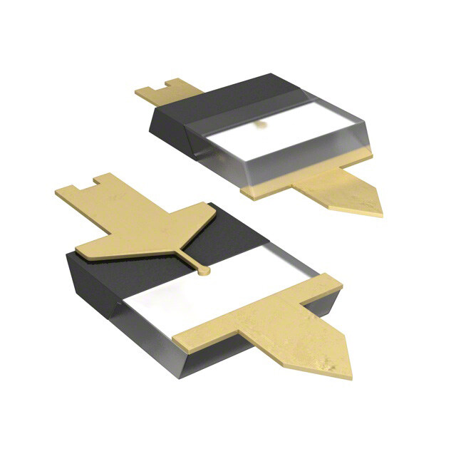
HPND-4028, HPND-4038 Beam Lead PIN Diodes for Phased Arrays and Switches Data Sheet Description Features The HPND-4028 and 4038 beam lead PIN diodes are • Low Capacitance designed for low capacitance, low resistance, and fast 0.025 pF Maximum at 1 MHz Guaranteed Min./Max. switching at microwave frequencies. These character- • Fast Switching istics are achieved at low bias levels for minimal power 2.0 nsec consumption. Advanced processing techniques ensure uniform and consistent electrical performance, allowing • Low Resistance at Low Bias guaranteed capacitance windows. This translates to 1.5 Ω at IF = 10 mA (Typical) improved performance in phased array applications. • Rugged Construction Typical 10 Gram Lead Pull Rugged construction and strong beams ensure high assembly yields while nitride passivation and polyimide • Silicon Nitride Passivation coating ensure reliability. Applications Outline 83 These beam lead PIN diodes are designed for use in stripline, coplanar waveguide, or microstrip circuits. Ap- 690 (27) 650 (26) plications include phase shifting and switching. The guaranteed capacitance windows ensure uniform per- 330 (13) formance in phased array radar. The low capacitance 260 (10) makes them ideal for circuits requiring high isolation in 220 (9) 180 (7) 180 (7) 160 (6) the series configuration. These devices have been fully characterized and S-parameters have been provided. Maximum Ratings 110 (4.5) 280 (11) Operating Temperature -65°C to +150°C 90 (3.5) 240 (9) Storage Temperature -65°C to +200°C Power Dissipation at T = 25°C 250 mW CASE (Derate linearly to zero at 150°C.) 8 (0.3) Min. Minimum Lead Strength 4 grams pull on either lead per MIL-S-19500, LTPD = 20 60 (2.4) 40 (1.6) DIMENSIONS IN µM (1/1000 INCH)
2 Electrical Specifications at TA = 25°C Break-down Reverse Forward Carrier Reverse Series Part Capacitance Series Resistance Voltage Current Voltage Lifetime Recovery Resistance Number (pF) R (Ω) V (V) I (nA) V (V) τ (ns) trr (ns) R (Ω) S BR R F S HPND- Min. Max. Typ. Max. Min. Max. Max. Typ. Typ. Typ. 4028 0.025 0.045 2.3 3.0 60 100 1.1 36 2.6 2.0 4038 0.045 0.065 1.5 2.0 60 100 1.1 45 2.4 1.0 Test V = 30 V I = 10 mA V = V V = 50 V I = 20 mA I = 10 mA *I = 10 mA I = 50 mA R F R BR R F F F F Conditions f = 1 MHz f = 100 MHz Measure I = 6 mA I = 5 mA f = 100 MHz R F I ≤ 10 mA V = 10 V 90% recovery R R Typical Parameters 30 0.12 26 40 22 0.10 35 30 18 B) 2205 B) 14 pF)0.08 ISOLATION (d 115050 -301510V 0mmV mAAA 0000....34670505 TION LOSS (dB) ISOLATION (d 1062 -31510 00mmV mVAAA 0000....2345 TION LOSS (dB) CAPACITANCE (000...000642 HHPPNNDD--44002388 R R 0.15 SE 0.1 SE 0 N 0 N 0 1 10 1820 I 1 10 20 100 I 0 10 20 30 FREQUENCY (GHz) FREQUENCY (GHz) REVERSE VOLTAGE (V) Figure 1. Typical Isolation and Figure 2. Typical Isolation and Figure 3. Typical Capacitance vs. Insertion Loss, HPND-4028. Insertion Loss, HPND-4038. Reverse Voltage (at 1 MHz). 12 100 1000 10 10 EVERSE RECOVERY TIME (nsec) 6842 VVnn == 1200VV FORWARD CURRENT (mA)0.00.111 RF RESISTANCE (OHMS)1101.000 HPND-4038 HPND-4028 R 0 0.001 0.1 0 5 10 15 0 0.2 0.4 0.6 0.8 1.0 0.01 0.10 1.0 10 100 FORWARD CURRENT (mA) FORWARD VOLTAGE (V) IF - FORWARD BIAS CURRENT (mA) Figure 4. Typical Reverse Recovery Figure 5. Typical Forward Figure 6. Typical RF Resistance vs. Time vs. Forward Current (Series Characteristics. Forward Bias Current (at 100 MHz). Configuration). HPND-4028, HPND- 4038.
3 Typical S-Parameters (in series configuration) at Z = 50 Ω, 25°C O HPND-4028 I = 1 mA I = 5 mA I = 10 mA F F F Freq. S /S S /S S /S S /S S /S S /S 11 22 21 12 11 22 21 12 11 22 21 12 (MHz) Mag. Ang. dB Mag. Ang. Mag. Ang. dB Mag. Ang. Mag. Ang. dB Mag. Ang. 1000 0.046 7 -0.38 0.958 -1 0.031 17 -0.24 0.973 -1 0.027 19 -0.20 0.978 -1 2000 0.048 20 -0.40 0.956 -2 0.036 33 -0.26 0.971 -2 0.033 37 -0.22 0.975 -2 3000 0.052 29 -0.40 0.957 -4 0.041 43 -0.26 0.972 -4 0.040 47 -0.22 0.975 -4 4000 0.058 36 -0.40 0.957 -5 0.049 49 -0.26 0.971 -5 0.047 53 -0.22 0.975 -5 5000 0.063 42 -0.40 0.956 -6 0.057 54 -0.26 0.971 -6 0.055 58 -0.22 0.975 -6 6000 0.069 46 -0.40 0.956 -7 0.064 57 -0.26 0.971 -7 0.063 60 -0.24 0.974 -7 7000 0.075 48 -0.40 0.956 -8 0.070 60 -0.26 0.971 -8 0.070 62 -0.22 0.975 -8 8000 0.081 50 -0.40 0.955 -9 0.077 60 -0.28 0.970 -9 0.076 63 -0.24 0.974 -9 9000 0.087 51 -0.40 0.956 -11 0.084 61 -0.28 0.970 -11 0.083 63 -0.24 0.974 -11 10000 0.092 52 -0.40 0.956 -12 0.089 61 -0.28 0.970 -12 0.089 63 -0.24 0.974 -12 11000 0.097 53 -0.40 0.956 -13 0.095 61 -0.26 0.971 -13 0.095 63 -0.22 0.975 -13 12000 0.103 52 -0.40 0.956 -14 0.101 60 -0.26 0.971 -14 0.101 62 -0.22 0.975 -14 13000 0.107 51 -0.40 0.957 -15 0.106 59 -0.26 0.971 -15 0.105 62 -0.22 0.975 -15 14000 0.112 51 -0.42 0.954 -17 0.110 59 -0.30 0.968 -17 0.111 61 -0.24 0.973 -17 15000 0.119 51 -0.42 0.953 -18 0.117 58 -0.28 0.969 -18 0.117 60 -0.26 0.972 -18 16000 0.123 51 -0.44 0.952 -19 0.122 57 -0.28 0.969 -19 0.123 60 -0.26 0.972 -19 17000 0.129 49 -0.44 0.952 -20 0.130 56 -0.30 0.967 -20 0.129 57 -0.26 0.971 -20 18000 0.139 48 -0.46 0.950 -22 0.139 55 -0.32 0.965 -21 0.140 56 -0.28 0.970 -22 HPND-4028 V = 0 V V = 10 V V = 30 V R R R Freq. S /S S /S S /S S /S S /S S /S 11 22 21 12 11 22 21 12 11 22 21 12 (MHz) Mag. Ang. dB Mag. Ang. Mag. Ang. dB Mag. Ang. Mag. Ang. dB Mag. Ang. 1000 0.997 -4 -27.54 0.042 86 0.999 -3 -33.16 0.022 91 1.000 -2 -33.98 0.020 91 2000 0.988 -7 -21.74 0.082 79 0.997 -6 -27.34 0.043 86 0.998 -5 -28.18 0.039 86 3000 0.974 -11 -18.36 0.121 74 0.994 -8 -23.62 0.066 83 0.996 -7 -24.44 0.060 84 4000 0.958 -14 -16.10 0.157 69 0.991 -10 -21.12 0.088 81 0.992 -10 -21.94 0.080 82 5000 0.940 -17 -14.48 0.189 64 0.986 -13 -19.26 0.109 78 0.987 -13 -20.10 0.099 79 6000 0.921 -21 -13.20 0.219 70 0.979 -16 -17.66 0.131 75 0.982 -15 -18.42 0.120 76 7000 0.898 -24 -12.16 0.247 56 0.972 -19 -16.26 0.054 72 0.976 -18 -17.08 0.140 73 8000 0.879 -26 -11.36 0.271 52 0.965 -21 -15.20 0.174 70 0.970 -21 -15.92 0.160 71 9000 0.857 -29 -10.64 0.294 48 0.954 -24 -14.20 0.195 67 0.960 -23 -14.96 0.179 68 10000 0.836 -32 -10.12 0.312 46 0.942 -27 -13.44 0.213 65 0.950 -26 -14.20 0.195 66 11000 0.816 -35 -9.54 0.334 42 0.931 -30 -12.58 0.235 61 0.937 -29 -13.32 0.216 62 12000 0.795 -37 -9.10 0.351 40 0.917 -33 -11.84 0.256 59 0.926 -32 -12.62 0.234 60 13000 0.778 -40 -8.86 0.361 37 0.904 -36 -11.44 0.268 56 0.913 -34 -12.20 0.246 57 14000 0.761 -42 -8.44 0.379 33 0.892 -38 -10.80 0.289 52 0.903 -37 -11.52 0.266 54 15000 0.744 -44 -8.34 0.383 31 0.876 -41 -10.56 0.297 50 0.888 -39 -11.26 0.274 52 16000 0.733 -46 -8.04 0.397 28 0.867 -43 -10.12 0.312 46 0.881 -42 -10.80 0.289 48 17000 0.720 -48 -7.94 0.401 26 0.855 -45 -9.96 0.318 44 0.869 -44 -10.64 0.294 46 18000 0.709 -50 -8.00 0.399 24 0.846 -47 -9.94 0.319 42 0.861 -46 -10.64 0.294 44
4 Typical S-Parameters (in series configuration) at Z = 50 Ω, 25°C (cont.) O HPND-4038 I = 1 mA I = 5 mA I = 10 mA F F F Freq. S /S S /S S /S S /S S /S S /S 11 22 21 12 11 22 21 12 11 22 21 12 (MHz) Mag. Ang. dB Mag. Ang. Mag. Ang. dB Mag. Ang. Mag. Ang. dB Mag. Ang. 1000 0.028 15 -0.22 0.976 -1 0.019 28 -0.12 0.987 -1 0.017 35 -0.10 0.989 -1 2000 0.032 34 -0.24 0.974 -2 0.026 50 -0.16 0.984 -2 0.024 56 -0.14 0.986 -2 3000 0.037 47 -0.22 0.975 -3 0.034 61 -0.14 0.985 -3 0.033 66 -0.12 0.988 -4 4000 0.045 55 -0.22 0.975 -5 0.042 67 -0.14 0.985 -5 0.042 70 -0.12 0.987 -5 5000 0.052 61 -0.24 0.974 -6 0.051 72 -0.16 0.984 -6 0.051 75 -0.14 0.986 -6 6000 0.060 65 -0.24 0.974 -7 0.059 74 -0.16 0.984 -7 0.059 77 -0.14 0.986 -7 7000 0.067 67 -0.24 0.974 -8 0.067 76 -0.16 0.984 -8 0.067 78 -0.12 0.987 -8 8000 0.073 69 -0.24 0.974 -9 0.074 76 -0.16 0.983 -9 0.073 78 -0.14 0.986 -9 9000 0.081 70 -0.24 0.973 -10 0.081 77 -0.16 0.984 -10 0.081 78 -0.14 0.986 -10 10000 0.087 71 -0.24 0.974 -11 0.088 77 -0.16 0.982 -11 0.089 79 -0.14 0.986 -11 11000 0.092 71 -0.22 0.975 -12 0.094 77 -0.16 0.984 -12 0.094 79 -0.14 0.986 -12 12000 0.099 70 -0.24 0.974 -14 0.100 76 -0.16 0.984 -14 0.101 77 -0.14 0.986 -14 13000 0.104 70 -0.22 0.975 -15 0.106 75 -0.14 0.985 -15 0.107 76 -0.12 0.987 -15 14000 0.110 69 -0.26 0.972 -16 0.112 74 -0.16 0.982 -16 0.113 75 -0.16 0.984 -16 15000 0.118 67 -0.24 0.973 -17 0.119 72 -0.16 0.983 -17 0.120 73 -0.14 0.985 -17 16000 0.123 66 -0.24 0.973 -18 0.125 71 -0.16 0.982 -18 0.126 72 -0.16 0.984 -18 17000 0.132 64 -0.26 0.972 -19 0.133 68 -0.16 0.982 -19 0.133 69 -0.16 0.984 -19 18000 0.141 62 -0.26 0.972 -20 0.143 66 -0.18 0.980 -20 0.143 67 -0.16 0.983 -20 HPND-4038 V = 0 V V = 10 V V = 30 V R R R Freq. S /S S /S S /S S /S S /S S /S 11 22 21 12 11 22 21 12 11 22 21 12 (MHz) Mag. Ang. dB Mag. Ang. Mag. Ang. dB Mag. Ang. Mag. Ang. dB Mag. Ang. 1000 0.993 -5 -23.10 0.070 83 0.998 -3 -28.88 0.036 89 0.999 -3 -29.90 0.032 90 2000 0.976 -10 -17.28 0.137 76 0.995 -7 -22.86 0.072 84 0.996 -6 -23.76 0.065 85 3000 0.953 -15 -14.04 0.199 70 0.990 -10 -19.26 0.109 81 0.992 -9 -20.18 0.098 82 4000 0.923 -19 -11.88 0.255 64 0.982 -13 -16.78 0.145 78 0.986 -12 -17.74 0.130 79 5000 0.890 -23 -10.36 0.304 58 0.973 -16 -14.90 0.180 74 0.977 -15 -15.88 0.161 75 6000 0.857 -27 -9.20 0.347 53 0.962 -20 -13.40 0.214 71 0.968 -19 -14.30 0.193 73 7000 0.822 -31 -8.28 0.386 49 0.947 -23 -12.08 0.249 68 0.956 -22 -12.96 0.225 69 8000 0.790 -34 -7.58 0.418 45 0.933 -27 -11.06 0.280 65 0.945 -25 -11.92 0.254 66 9000 0.757 -38 -7.00 0.447 41 0.915 -30 -10.12 0.312 61 0.928 -29 -10.94 0.284 63 10000 0.727 -41 -6.54 0.471 38 0.897 -34 -9.40 0.339 58 0.912 -32 -10.22 0.309 61 11000 0.697 -44 -6.10 0.496 34 0.877 -37 -8.62 0.371 54 0.892 -35 -9.44 0.338 57 12000 0.668 -46 -5.74 0.517 32 0.854 -41 -8.00 0.399 52 0.874 -38 -8.76 0.365 54 13000 0.643 -49 -5.56 0.528 29 0.834 -44 -7.60 0.417 49 0.854 -42 -8.34 0.383 51 14000 0.620 -51 -5.22 0.549 26 0.813 -47 -7.04 0.445 45 0.839 -45 -7.76 0.410 48 15000 0.599 -53 -5.16 0.553 24 0.793 -50 -6.82 0.457 43 0.818 -48 -7.50 0.422 45 16000 0.584 -55 -4.90 0.569 21 0.778 -53 -6.42 0.478 39 0.805 -50 -7.10 0.442 42 17000 0.570 -57 -4.80 0.576 19 0.762 -55 -6.22 0.489 37 0.790 -53 -6.88 0.453 40 18000 0.556 -59 -4.84 0.574 17 0.747 -58 -6.18 0.491 35 0.776 -55 -6.86 0.454 37
5 Bonding and Handling Procedures for Beam Lead Diodes 4. Bonding 1. Storage Thermocompression: See Application Note 979 “The Handling and Bonding of Beam Lead Devices Made Under normal circumstances, storage of beam lead Easy”. This method is good for hard substrates only. diodes in Avago supplied waffle/gel packs is sufficient. In particularly dusty or chemically hazardous environ- Wobble: This method picks up the device, places it on ments, storage in an inert atmosphere desiccator is the substrate and forms a thermo-compression bond all advised. in one operation. This is described in the latest version of MIL-STD-883, Method 2017, and is intended for hard 2. Handling substrates only. In order to avoid damage to beam lead devices, par- ticular care must be exercised during inspection, Resistance Welding or Parallel-GAP Welding: To make testing, and assembly. Although the beam lead diode welding on soft substrates easier, a low pressure welding is designed to have exceptional lead strength, its small head is recommended. Suitable equipment is available size and delicate nature requires that special handling from HUGHES, Industrial Products Division in Carlsbad, techniques be observed so that the devices will not be CA. mechanically or electrically damaged. A vacuum pickup Epoxy: With solvent free, low resistivity epoxies is recommended for picking up beam lead devices, par- (available from ABLESTIK and improvements in dispens- ticularly larger ones, e.g., quads. Care must be exercised ing equipment, the quality of epoxy bonds is sufficient to assure that the vacuum opening of the needle is suf- for many applications. ficiently small to avoid passage of the device through the opening. A #27 tip is recommended for picking up 5. Lead Stress single beam lead devices. A 20X magnification is needed In the process of bonding a beam lead diode, a certain for precise positioning of the tip on the device. Where a amount of “bugging” occurs. The term bugging refers vacuum pickup is not used, a sharpened wooden Q-tip to the chip lifting away from the substrate during the dipped in isopropyl alcohol is very commonly used to bonding process due to the deformation of the beam by handle beam lead devices. the bonding tool. This effect is beneficial as it provides 3. Cleaning stress relief for the diode during thermal cycling of the substrate. The coefficient of expansion of some substrate For organic contamination use a warm rinse of trichlo- materials, specifically soft substrates, is such that some roethane, or its locally approved equivalent, followed by bugging is essential if the circuit is to be operated over a cold rinse in acetone and methanol. Dry under infrared wide temperature extremes. heat lamp for 5–10 minutes on clean filter paper. Freon degreaser, or its locally approved equivalent, may Thick metal clad ground planes restrict the thermal replace trichloroethane for light organic contamination. expansion of the dielectric substrates in the X-Y axis. The expansion of the dielectric will then be mainly • Ultrasonic cleaning is not recommended. in the Z axis, which does not affect the beam lead • Acid solvents should not be used. device. An alternate solution to the problem of dielec- tric ground plane expansion is to heat the substrate to the maximum required operating temperature during the beam lead attachment. Thus, the substrate is at maximum expansion when the device is bonded. Sub- sequent cooling of the substrate will cause bugging, similar to bugging in thermocompression bonding or epoxy bonding. Other methods of bugging are pre- forming the leads during assembly or prestressing the substrate.
For product information and a complete list of distributors, please go to our web site: www.avagotech.com Avago, Avago Technologies, and the A logo are trademarks of Avago Technologies Limited in the United States and other countries. Data subject to change. Copyright © 2006 Avago Technologies Limited. All rights reserved. Obsoletes 5967-6157E AV01-0594EN - October 20, 2006