ICGOO在线商城 > 射频/IF 和 RFID > RF 混频器 > HMC615LP4E
 Datasheet下载
- 型号: HMC615LP4E
- 制造商: Hittite
- 库位|库存: xxxx|xxxx
- 要求:
| 数量阶梯 | 香港交货 | 国内含税 |
| +xxxx | $xxxx | ¥xxxx |
查看当月历史价格
查看今年历史价格
HMC615LP4E产品简介:
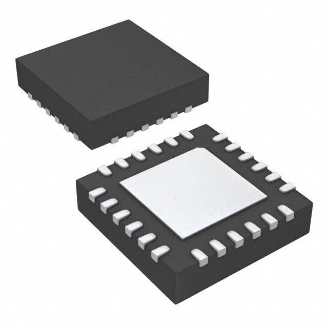
ICGOO电子元器件商城为您提供HMC615LP4E由Hittite设计生产,在icgoo商城现货销售,并且可以通过原厂、代理商等渠道进行代购。 HMC615LP4E价格参考。HittiteHMC615LP4E封装/规格:RF 混频器, RF Mixer IC WiMAX / WiBro Up/Down Converter 2.3GHz ~ 4GHz 24-QFN (4x4)。您可以下载HMC615LP4E参考资料、Datasheet数据手册功能说明书,资料中有HMC615LP4E 详细功能的应用电路图电压和使用方法及教程。
HMC615LP4E是Analog Devices Inc.推出的一款高性能RF混频器,主要应用于微波和毫米波通信系统。该器件工作频率范围宽,典型应用包括点对点无线通信、微波回传链路、卫星通信以及雷达系统等高频场景。其高线性度和低转换损耗特性使其非常适合用于要求严苛的宽带基础设施设备中。

HMC615LP4E采用无源双平衡设计,具备良好的端口隔离性能和较强的抗干扰能力,可在无需额外放大器的情况下实现高效信号混频,适用于上变频和下变频电路。由于其封装紧凑(4×4 mm QFN),便于集成于高密度PCB布局中,广泛用于基站收发设备、测试仪器及军用通信平台。

此外,该混频器在工业温度范围内稳定工作,适合恶劣环境下的长期运行,因此也常见于航空航天与国防领域的电子战和信号监测系统中。总体而言,HMC615LP4E是一款面向高端射频系统的可靠核心元件,适用于对性能和稳定性要求较高的无线传输与接收应用。
| 参数 | 数值 |
| 产品目录 | |
| 描述 | IC MMIC MIXER HIGH IP3 24-QFN |
| 产品分类 | |
| 品牌 | Hittite Microwave Corporation |
| 数据手册 | |
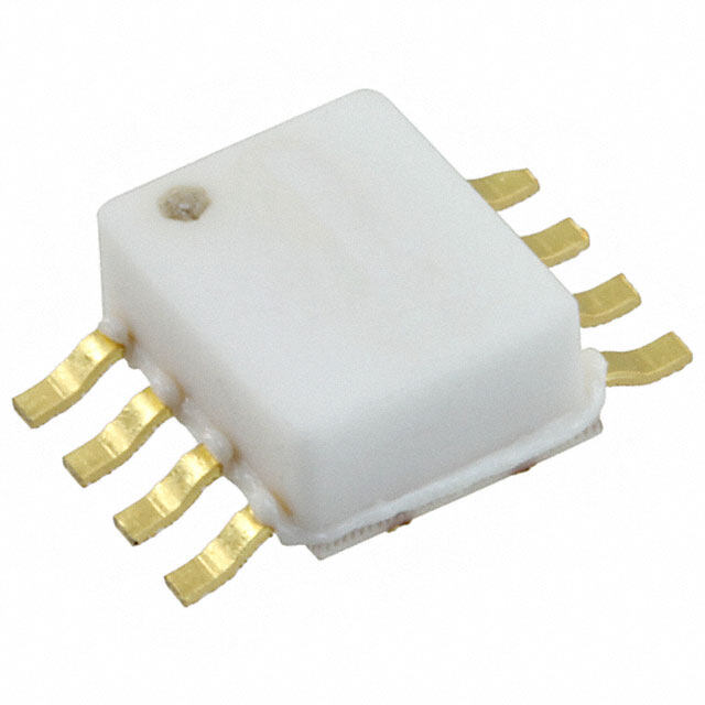
| 产品图片 |
|
| 产品型号 | HMC615LP4E |
| RF类型 | WiMAX / WiBro |
| rohs | 无铅 / 符合限制有害物质指令(RoHS)规范要求 |
| 产品系列 | - |
| 供应商器件封装 | 24-QFN(4x4) |
| 其它名称 | 1127-1483 |
| 包装 | 剪带 |
| 噪声系数 | 10dB |
| 增益 | - |
| 封装/外壳 | 24-VFQFN 裸露焊盘 |
| 标准包装 | 100 |
| 混频器数 | 1 |
| 电压-电源 | 5V |
| 电流-电源 | 65mA |
| 辅助属性 | 升/降频器 |
| 频率 | 2.3GHz ~ 4GHz |


- 商务部:美国ITC正式对集成电路等产品启动337调查
- 曝三星4nm工艺存在良率问题 高通将骁龙8 Gen1或转产台积电
- 太阳诱电将投资9.5亿元在常州建新厂生产MLCC 预计2023年完工
- 英特尔发布欧洲新工厂建设计划 深化IDM 2.0 战略
- 台积电先进制程称霸业界 有大客户加持明年业绩稳了
- 达到5530亿美元!SIA预计今年全球半导体销售额将创下新高
- 英特尔拟将自动驾驶子公司Mobileye上市 估值或超500亿美元
- 三星加码芯片和SET,合并消费电子和移动部门,撤换高东真等 CEO
- 三星电子宣布重大人事变动 还合并消费电子和移动部门
- 海关总署:前11个月进口集成电路产品价值2.52万亿元 增长14.8%


PDF Datasheet 数据手册内容提取
HMC615LP4 / 615LP4E v03.0412 GaAs MMIC MIXER w/ INTEGRATED LO AMPLIFIER, 2.3 - 4.0 GHz Typical Applications Features The HMC615LP4e is ideal for: High input iP3: +35 dBm T • PCS / 3G Infrastructure Low input LO Drive: -2 to +6 dBm M • Base Stations & Repeaters Low Conversion Loss: 10 dB s E • WiMAX & WiBro single Positive supply: +5V @ 65 mA - 3 • ISM & Fixed Wireless 24 Lead 4x4mm QFN Package: 9 mm² P T i H g i Functional Diagram General DeEscription H The HMC615LP4(e) are high linearity, gaAs FeT - s converter iCs that operate from 2.3 to 4.0 gHz and r delivLer a +35 dBm input third order intercept point. e The LO amplifier output and high dynamic range x mixer input are positioned so that an external LO i O filter can be placed in series between them. The iC M operates from a single +5V supply consuming 65 mA of current and accepts a LO drive level of -2 to +6 dBm. The design requires no external baluns and S supports iF frequencies between DC and 1 gHz. The HMC615LP4(e) is pin for pin compatible with the HMC551LP4(e), HMC552LP4(e) and HMC215LP4(e), B which operate from 0.8 to 4.0 gHz. For availability on Non-roHs HMC615LP4 products please contact Hittite Microwave sales directly. O Electrical Specifications, T = +25° C, LO = 4 dBm, Vcc = +5V, R1 = 18 Ohms, IF = 200 MHz* A Parameter Min. Typ. Max. Units Frequency range, rF, LO 2.3 - 4.0 gHz Frequency range, iF DC - 1.0 gHz Conversion Loss * 10 13 dB Noise Figure (ssB) 10 dB LO to rF isolation 5 15 dB LO to iF isolation * 1 10 dB iP3 (input) 35 dBm 1 dB Compression (input) 21 dBm LO Drive input Level (Typical) -2 to +6 dBm supply Current (icc) 65 75 mA *Unless otherwise noted, all measurements performed as a downconverter configured as shown in application circuit. For price, delivery and to place orders: Hittite Microwave Corporation, 2 Elizabeth Drive, Chelmsford, MA 01824 1 Phone: 978-250-3343 Fax: 978-250-3373 Order On-line at www.hittite.com Application Support: Phone: 978-250-3343 or apps@hittite.com
HMC615LP4 / 615LP4E vv0023..10241102 GaAs MMIC MIXER w/ INTEGRATED LO AMPLIFIER, 2.3 - 4.0 GHz Conversion Gain vs. Temperature @ LO = 4 dBm Isolation @ LO = 4 dBm 0 0 T -5 B) +25C M RSION GAIN (d-1-05 +-4805CC LATION (dB)--1150 E 3 - s E O RF to IF CONV-15 IS-20 LLOO ttoo RIFFT iP -25 H g -20 -30 1.5 2 2.5 3 3.5 4 4.5 1.5 2E2.5 3 3.5 4 4.5 i H FREQUENCY (GHz) FREQUENCY (GHz) - s L r Conversion Gain vs. LO Drive Return Loss @ LO = 4 dBm e 0 0 x O i M LO= -4 dBm -5 B) LO= -2 dBm GAIN (d -5 LLLLOOOO==== 0246 ddddBBBBmmmm SS (dB)-10 N O ONVERSIO--1150 S RETURN L--2105 C -25 LO B RF -20 -30 1.5 2 2.5 3 3.5 4 4.5 1.5 2 2.5 3 3.5 4 4.5 FREQUENCY (GHz) FREQUENCY (GHz) O Upconverter Performance (IF= 100 MHz) Conversion Gain vs. LO Drive IF Bandwidth @ LO = 4 dBm 0 0 LO= -4 dBm dB) -5 LLOO== - 02 ddBBmm -5 CRoentuvernrs Lioons sGain GAIN ( LLLOOO=== 246 dddBBBmmm E (dB)-10 N S O-10 N NVERSI RESPO-15 O-15 C -20 -20 -25 1.5 2 2.5 3 3.5 4 4.5 0 0.5 1 1.5 2 2.5 FREQUENCY (GHz) FREQUENCY (GHz) For price, delivery and to place orders: Hittite Microwave Corporation, 2 Elizabeth Drive, Chelmsford, MA 01824 Phone: 978-250-3343 Fax: 978-250-3373 Order On-line at www.hittite.com 2 Application Support: Phone: 978-250-3343 or apps@hittite.com
HMC615LP4 / 615LP4E v03.0412 GaAs MMIC MIXER w/ INTEGRATED LO AMPLIFIER, 2.3 - 4.0 GHz Input IP3 vs. Temperature @ LO = 4 dBm Input IP3 vs. LO Drive 50 50 T M 40 40 s m) 30 m) 30 E B B - d d 3 IP3 ( 20 ++ 2855CC IP3 ( 20 P - 40C TLO= -2 dBm i LO= 0 dBm 10 10 LO= 2 dBm H LO= 4 dBm LO= 6 dBm g 0 0 i 1.8 2.2 2.6 3 3.4 3.8 4.2 1.8 2.E2 2.6 3 3.4 3.8 4.2 H FREQUENCY (GHz) FREQUENCY (GHz) - s r L Input IP2 vs. Temperature @ LO = 4 dBm Input IP2 vs. LO Drive e x 50 50 i O M 40 40 m) 30 m) 30 B B d d 2 ( S 2 ( IP 20 IP 20 LO= -2 dBm + 25C LO= 0 dBm 10 + 85C 10 LO= 2 dBm - 40C LO= 4 dBm B LO= 6 dBm 0 0 1.8 2.2 2.6 3 3.4 3.8 4.2 1.8 2.2 2.6 3 3.4 3.8 4.2 FREQUENCY (GHz) FREQUENCY (GHz) O Input P1dB vs. Temperature @ LO = 4 dBm MxN Spurious @ IF Port 30 nLO mrF 0 1 2 3 4 25 0 xx -11 -1 6 10 m) 1 5 0 16 37 36 B d 2 58 67 55 51 60 B ( 20 1d 3 98 102 103 82 91 P 4 99 99 104 106 107 +25C 15 +85C -40C rF Freq. = 3 gHz @ -10 dBm LO Freq. = 2.8 gHz @ 0 dBm All values in dBc relative to the iF power level. 10 1.7 2.1 2.5 2.9 3.3 3.7 4.1 FREQUENCY (GHz) For price, delivery and to place orders: Hittite Microwave Corporation, 2 Elizabeth Drive, Chelmsford, MA 01824 3 Phone: 978-250-3343 Fax: 978-250-3373 Order On-line at www.hittite.com Application Support: Phone: 978-250-3343 or apps@hittite.com
HMC615LP4 / 615LP4E v03.0412 GaAs MMIC MIXER w/ INTEGRATED LO AMPLIFIER, 2.3 - 4.0 GHz Absolute Maximum Ratings Harmonics of LO RF / IF Input (Vcc= +5V) +27 dBm nLO spur @ rF Port LO Drive (Vcc= +5V) +10 dBm LO Freq. (gHz) 1 2 3 4 BiAs +7 Vdc T 1 8 13 29 31 Junction Temperature 150°C M 1.8 5 23 18 34 Continuous Pdiss (T = 85°C) 0.339 W 2.6 11 12 E27 30 s (derate 5.21 mW/°C above 85°C) 3.4 15 16 48 27 - T(juhnecrmtioanl rtoe sgirsotuanndc epaddle) 192 °C/W 4.2 7 18 27 27 3 5 16 27 38 43 P storage Temperature -65 to +150°C T LO = 0 dBm i Operating Temperature -40 to +85°C All values in dBc below input LO level measured at rF port. H g Typical Supply Current E i H eLeCTrOsTATiC seNsiTiVe DeViCe Vcc icc (mA) OBserVe HANDLiNg PreCAUTiONs - +5.0 65 mA s Outline Drawing L r e x O i M S B O NOTes: 1. LeADFrAMe MATeriAL: COPPer ALLOY 2. DiMeNsiONs Are iN iNCHes [MiLLiMeTers] 3. LeAD sPACiNg TOLerANCe is NON-CUMULATiVe. 4. PAD BUrr LeNgTH sHALL Be 0.15mm MAxiMUM. PAD BUrr HeigHT sHALL Be 0.05mm MAxiMUM. 5. PACKAGE WARP SHALL NOT EXCEED 0.05mm. 6. ALL grOUND LeADs AND grOUND PADDLe MUsT Be sOLDereD TO PCB rF grOUND. 7. reFer TO HiTTiTe APPLiCATiON NOTe FOr sUggesTeD LAND PATTerN. Package Information Part Number Package Body Material Lead Finish MsL rating Package Marking [3] HMC615LP4 Low stress injection Molded Plastic[4] Sn/Pb Solder MsL1 [1] H615 xxxx HMC615LP4e roHs-compliant Low stress injection Molded Plastic 100% matte sn MsL1 [2] H615 xxxx [1] Max peak reflow temperature of 235 °C [2] Max peak reflow temperature of 260 °C [3] 4-Digit lot number xxxx [4] For availability of Non-roHs HMC615LP4 products please contact Hittite Microwave sales directly. For price, delivery and to place orders: Hittite Microwave Corporation, 2 Elizabeth Drive, Chelmsford, MA 01824 Phone: 978-250-3343 Fax: 978-250-3373 Order On-line at www.hittite.com 4 Application Support: Phone: 978-250-3343 or apps@hittite.com
HMC615LP4 / 615LP4E v03.0412 GaAs MMIC MIXER w/ INTEGRATED LO AMPLIFIER, 2.3 - 4.0 GHz Pin Descriptions Pin Number Function Description interface schematic T M This pin is DC coupled and matched to 50 Ohms. 1 Mix LO s An off chip DC blocking capacitor is required. E - 3 P 2, 6 - 9, No connection. These pins may be connected to rF N/C 11 - 17, 19 - 24 ground. Performance will not be affected. T i H g i Power supply for the LO amplifier , a Bias resistor is E H required. Three external bypass capacitors are recom- 3 BiAs mended for optimum performance, as illustrated in the - application circuit. s r L e x 4 gND Backside of package has exposed metal ground paddle that must also be connected to ground. i O M This pin is DC coupled and matched to 50 Ohms. 5 LO An off chip DC blocking capacitor is required. S This pin is DC coupled. For applications not requiring operation to DC, this port should be DC blocked Bexternally using a series capacitor whose value has 10 iF been chosen to pass the necessary iF frequency range. For operation to DC, this pin must not source/ sink more than 18 mA of current or die non-function and possible die failure will result. O This pin is DC coupled and 18 rF matched to 50 Ohms. For price, delivery and to place orders: Hittite Microwave Corporation, 2 Elizabeth Drive, Chelmsford, MA 01824 5 Phone: 978-250-3343 Fax: 978-250-3373 Order On-line at www.hittite.com Application Support: Phone: 978-250-3343 or apps@hittite.com
HMC615LP4 / 615LP4E v03.0412 GaAs MMIC MIXER w/ INTEGRATED LO AMPLIFIER, 2.3 - 4.0 GHz Application Circuit T M E s - 3 P T i H g E i H - Evaluation PCB s Lrecommended Components Values (iF = DC - 300 MHz) r C3 1000 pF e C4 2.2 µF x O C1, C2, C5 100 pF i M L1 18 nH r1 18 Ohm S B Note : select r1 to achieve icc by using equation below, r1 ≥ 18 Ohms. O Icc = ( Vs - 3.8 ) / R1 List of Materials for Evaluation PCB 115906 [1] The circuit board used in the application should use item Description rF circuit design techniques. signal lines should J1 - J3 PCB Mount sMA rF Connector J4, J5 DC Pin have 50 Ohm impedance while the package ground C1, C2, C5 100 pF Chip Capacitor, 0402 Pkg. leads and exposed paddle should be connected C3 1000 pF Chip Capacitor, 0603 Pkg. directly to the ground plane similar to that shown. C4 2.2 µF Capacitor, Tantalum A sufficient number of via holes should be used to L1 18 nH Chip inductor, 0603 Pkg. connect the top and bottom ground planes. The r1 18 Ohm Resistor, 1210 1/8 watt Pkg. evaluation circuit board shown is available from Hit- U1 HMC615LP4e tite upon request. PCB [2] 113417 evaluation Board [1] reference this number when ordering complete evaluation PCB [2] Circuit Board Material: rogers 4350 For price, delivery and to place orders: Hittite Microwave Corporation, 2 Elizabeth Drive, Chelmsford, MA 01824 Phone: 978-250-3343 Fax: 978-250-3373 Order On-line at www.hittite.com 6 Application Support: Phone: 978-250-3343 or apps@hittite.com