ICGOO在线商城 > 集成电路(IC) > 接口 - 模拟开关,多路复用器,多路分解器 > HI9P0201-5Z96

 Datasheet下载
- 型号: HI9P0201-5Z96
- 制造商: Intersil
- 库位|库存: xxxx|xxxx
- 要求:
| 数量阶梯 | 香港交货 | 国内含税 |
| +xxxx | $xxxx | ¥xxxx |
查看当月历史价格
查看今年历史价格
HI9P0201-5Z96产品简介:
ICGOO电子元器件商城为您提供HI9P0201-5Z96由Intersil设计生产,在icgoo商城现货销售,并且可以通过原厂、代理商等渠道进行代购。 HI9P0201-5Z96价格参考。IntersilHI9P0201-5Z96封装/规格:接口 - 模拟开关,多路复用器,多路分解器, 4 Circuit IC Switch 1:1 80 Ohm 16-SOIC。您可以下载HI9P0201-5Z96参考资料、Datasheet数据手册功能说明书,资料中有HI9P0201-5Z96 详细功能的应用电路图电压和使用方法及教程。
Renesas Electronics America Inc.的HI9P0201-5Z96是一款模拟开关/多路复用器器件,属于高性能、低电压、单刀双掷(SPDT)模拟开关。该器件广泛应用于需要高效信号路由和切换的电子系统中。

主要应用场景包括:

1. 通信设备:用于信号路径选择、频段切换或天线切换,在无线基站、路由器和交换设备中实现快速可靠的信号控制。

2. 工业控制系统:在数据采集系统或多通道传感器系统中,用于切换不同传感器输入信号,提升系统灵活性与集成度。

3. 测试与测量仪器:作为多路复用器使用时,可自动切换多个被测信号进入测量电路,提高测试效率和精度。

4. 医疗设备:用于多通道生理信号采集系统中,如心电图机、监护仪等,实现对多个传感器信号的选择性接入。

5. 消费电子产品:在音频/视频切换设备中应用,实现多路音视频信号的快速切换,适用于便携式多媒体设备或智能家居控制系统。

HI9P0201-5Z96具有低导通电阻、高速切换、小封装等特点,适合空间受限且对性能要求较高的应用场合。
| 参数 | 数值 |
| 产品目录 | 集成电路 (IC) |
| 描述 | IC SWITCH QUAD SPST 16SOIC |
| 产品分类 | |
| 品牌 | Intersil |
| 数据手册 | |
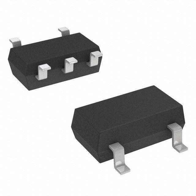
| 产品图片 |
|
| 产品型号 | HI9P0201-5Z96 |
| PCN组件/产地 | |
| rohs | 无铅 / 符合限制有害物质指令(RoHS)规范要求 |
| 产品系列 | - |
| 产品目录页面 | |
| 供应商器件封装 | 16-SOIC |
| 其它名称 | HI9P0201-5Z96CT |
| 功能 | |
| 包装 | 剪切带 (CT) |
| 安装类型 | 表面贴装 |
| 导通电阻 | 80 欧姆 |
| 封装/外壳 | 16-SOIC(0.154",3.90mm 宽) |
| 工作温度 | 0°C ~ 75°C |
| 标准包装 | 1 |
| 电压-电源,单/双 (±) | ±15V |
| 电压源 | 双电源 |
| 电流-电源 | 500µA |
| 电路 | 4 x SPST - NC |


- 商务部:美国ITC正式对集成电路等产品启动337调查
- 曝三星4nm工艺存在良率问题 高通将骁龙8 Gen1或转产台积电
- 太阳诱电将投资9.5亿元在常州建新厂生产MLCC 预计2023年完工
- 英特尔发布欧洲新工厂建设计划 深化IDM 2.0 战略
- 台积电先进制程称霸业界 有大客户加持明年业绩稳了
- 达到5530亿美元!SIA预计今年全球半导体销售额将创下新高
- 英特尔拟将自动驾驶子公司Mobileye上市 估值或超500亿美元
- 三星加码芯片和SET,合并消费电子和移动部门,撤换高东真等 CEO
- 三星电子宣布重大人事变动 还合并消费电子和移动部门
- 海关总署:前11个月进口集成电路产品价值2.52万亿元 增长14.8%


PDF Datasheet 数据手册内容提取
DATASHEET HI-200, HI-201 FN3121 Dual/Quad SPST, CMOS Analog Switches Rev 9.00 September 15, 2015 HI-200/HI-201 (dual/quad) are monolithic devices comprising Features independently selectable SPST switches which feature fast • Pb-Free Available (RoHS Compliant) switching speeds (HI-200 240ns, and HI-201 185ns) combined with low power dissipation (15mW at 25oC). Each • Analog Voltage Range. . . . . . . . . . . . . . . . . . . . . . . 15V switch provides low “ON” resistance operation for input signal • Analog Current Range. . . . . . . . . . . . . . . . . . . . . . . 80mA voltage up to the supply rails and for signal current up to 80mA. Rugged DI construction eliminates latch-up and • Turn-On Time. . . . . . . . . . . . . . . . . . . . . . . . . . . . . .240ns substrate SCR failure modes. • Low rON . . . . . . . . . . . . . . . . . . . . . . . . . . . . . . . . . . . 55 All devices provide break-before-make switching and are • Low Power Dissipation. . . . . . . . . . . . . . . . . . . . . . .15mW TTL and CMOS compatible for maximum application • TTL/CMOS Compatible versatility. HI-200/HI-201 are ideal components for use in high frequency analog switching. Typical applications Applications include signal path switching, sample and hold circuit, digital filters, and operational amplifier gain switching networks. • High Frequency Analog Switching Ordering Information • Sample and Hold Circuits TEMP. PKG. • Digital Filters PART NUMBER RANGE (°C) PACKAGE DWG. # • Operational Amplifier Gain Switching Networks HI3-0200-5Z 0 to 75 14 Ld PDIP* E14.3 (Note) (No (Pb-free) Functional Diagram longer available or supported) V+ VREF HI1-0201-2 -55 to 125 16 Ld CERDIP F16.3 INPUT HI3-0201-5Z 0 to 75 16 Ld PDIP* E16.3 SOURCE (Note) (Pb-free) GATE GATE HI4P0201-5Z 0 to 75 20 Ld PLCC N20.35 LOGIC REFERENCE, SWITCH (Note) (No (Pb-free) INPUT LEVEL SHIFTER, CELL longer available AND DRIVER DRAIN or supported) OUTPUT HI9P0201-5Z 0 to 75 16 Ld SOIC M16.15 V- (Note) (Pb-free) HI9P0201-9Z -40 to 85 16 Ld SOIC M16.15 (Note) (Pb-free) TRUTH TABLE *Pb-free PDIPs can be used for through hole wave solder processing only. They are not intended for use in Reflow solder LOGIC HI-200 HI-201 processing applications. 0 ON ON NOTE: Intersil Pb-free products employ special Pb-free material sets; 1 OFF OFF molding compounds/die attach materials and 100% matte tin plate ter- mination finish, which are RoHS compliant and compatible with both SnPb and Pb-free soldering operations. Intersil Pb-free products are MSL classified at Pb-free peak reflow temperatures that meet or ex- ceed the Pb-free requirements of IPC/JEDEC J STD-020. Pb-free PDIPs can be used for through hole wave solder processing only. They are not intended for use in Reflow solder processing applications. FN3121 Rev 9.00 Page 1 of 11 September 15, 2015
HI-200, HI-201 Pinouts (Switches Shown For Logic “1” Input) HI-200 (PDIP) HI-201 (CERDIP, PDIP, SOIC) HI-201 (PLCC) TOP VIEW TOP VIEW TOP VIEW A2 1 14 A1 D A1 1 16 A2 T1 T2 NC 2 13ONRTCE OUT1 2 15 OUT2 OU A1 NC A2 OU UPP 3 2 1 20 19 OGNUINNONT VCDL22-O N34567G ER AVAILA BLE O R S 11198201 VNIOVN+RCU1ETF1 OGUIINNNTVD144- 34576 1111114320 IVVIONN+RU23ETF3 GINNNVDC1- 4567 ER AVAILA BLE O R SUPP O RTE1111D6785 IVNVN+RC2EF A4 8 9 A3 N G IN4 8O LO 14 IN3 N 9 10 11 12 13 4 4 C 3 3 T A N A T U U O O Schematic Diagrams TTL/CMOS REFERENCE CIRCUIT VREF CELL TTL/CMOS REFERENCE CIRCUIT VREF CELL HI-200 HI-201 V+ V+ R6 R6 R2 300 R2 600 5K QP2 5K QP2 QP1 QP3 QP1 QP3 QN4 VREF QN4 VREF MP13 QP4 QP5 MP13 QP4 QP5 TO P2 TO P2 QN1 QN1 D3 R3 MN14 D3 R3 MN14 24.2K 24.2K R4 R4 MP14 QN2 5.4K QN2 5.4K VLL QN3 VLL R5 R5 GND 7.9K GND 7.9K QP6 MN15 MN16 MN17 R7 MN15 MN16 MN17 R7 100K 100K V- V- GND GND FN3121 Rev 9.00 Page 2 of 11 September 15, 2015
HI-200, HI-201 Schematic Diagrams (Continued) SWITCH CELL A’ QN11 V+ QN12 INPUT QP11 QN13 OUTPUT V- QP12 A’ DIGITAL INPUT BUFFER AND LEVEL SHIFTER V+ QP3 QP5 QP1 QP4 A’ V+ QN1 QP6 QP7 QP8 QP9 QP10 D1 TO VLL TO VREF QN8 QN9 QN10 200 D2 QN6 QN7 QP2 A V- A’ QN2 QN4 QN5 QN3 V- FN3121 Rev 9.00 Page 3 of 11 September 15, 2015
HI-200, HI-201 Absolute Maximum Ratings Thermal Information Supply Voltage (V+ to V-). . . . . . . . . . . . . . . . . . . . . . . . . 44V (22) Thermal Resistance (Typical, Note 1) JA (oC/W) JC (oC/W) VREF to Ground. . . . . . . . . . . . . . . . . . . . . . . . . . . . . . . . . 20V, -5V CERDIP Package. . . . . . . . . . . . . . . . . 75 20 Digital Input Voltage. . . . . . . . . . . . . . . . . . . . . .(V+) +4V to (V-) -4V PLCC Package. . . . . . . . . . . . . . . . . . . 80 N/A Analog Input Voltage (One Switch) . . . . . . . . . .(V+) +2V to (V-) -2V PDIP Package* . . . . . . . . . . . . . . . . . . 95 N/A SOIC Package. . . . . . . . . . . . . . . . . . . 110 N/A Operating Conditions Maximum Storage Temperature. . . . . . . . . . . . . . . . -65oC to 150oC Maximum Junction Temperature (Hermetic Packages). . . . . 175oC Temperature Ranges HI-201-2. . . . . . . . . . . . . . . . . . . . . . . . . . . . . . . . . . -55oC to 125oC Maximum Junction Temperature (Plastic Packages). . . . . . . 150oC HI-201-4. . . . . . . . . . . . . . . . . . . . . . . . . . . . . . . . . . . -25oC to 85oC Maximum Lead Temperature (Soldering, 10s). . . . . . . . . . . . 300oC HI-200-5, HI-201-5. . . . . . . . . . . . . . . . . . . . . . . . . . . . .0oC to 75oC (PLCC and SOIC - Lead Tips Only) HI-201-9. . . . . . . . . . . . . . . . . . . . . . . . . . . . . . . . . . . -40oC to 85oC *Pb-free PDIPs can be used for through hole wave solder process- ing only. They are not intended for use in reflow solder processing applications. CAUTION: Stresses above those listed in “Absolute Maximum Ratings” may cause permanent damage to the device. This is a stress only rating and operation of the device at these or any other conditions above those indicated in the operational sections of this specification is not implied. NOTE: 1. JA is measured with the component mounted on an evaluation PC board in free air. Electrical Specifications Supplies = +15V, -15V; VREF = Open; VAH (Logic Level High) = 2.4V, VAL (Logic Level Low) = 0.8V -2 -4, -5, -9 TEST TEMP PARAMETER CONDITIONS (oC) MIN TYP MAX MIN TYP MAX UNITS DYNAMIC CHARACTERISTICS Switch ON Time, tON HI-200 25 - 240 500 - 240 - ns HI-201 25 - 185 500 - 185 - ns Full - 1000 - - 1000 - ns Switch OFF Time, tOFF HI-200 25 - 330 500 - 500 - ns HI-201 25 - 220 500 - 220 - ns Full - 1000 - - 1000 - ns Off Isolation (Note 4) HI-200 25 - 70 - - 70 - dB HI-201 25 - 80 - - 80 - dB Input Switch Capacitance, CS(OFF) 25 - 5.5 - - 5.5 - pF Output Switch Capacitance, CD(OFF) 25 - 5.5 - - 5.5 - pF Output Switch Capacitance, CD(ON) 25 - 11 - - 11 - pF Digital Input Capacitance, CA 25 - 5 - - 5 - pF Drain-to-Source Capacitance, CDS(OFF) 25 - 0.5 - - 0.5 - pF DIGITAL INPUT CHARACTERISTICS Input Low Threshold, VAL Full - - 0.8 - - 0.8 V Input High Threshold, VAH Full 2.4 - - 2.4 - - V Input Leakage Current (High or Low), IA (Note 3) Full - - 1.0 - - 1.0 A ANALOG SWITCH CHARACTERISTICS Analog Signal Range, VS Full -15 - +15 -15 - +15 V ON Resistance, rON (Note 2) 25 - 55 70 - 55 80 Full - 80 100 - 72 100 FN3121 Rev 9.00 Page 4 of 11 September 15, 2015
HI-200, HI-201 Electrical Specifications Supplies = +15V, -15V; VREF = Open; VAH (Logic Level High) = 2.4V, VAL (Logic Level Low) = 0.8V (Continued) -2 -4, -5, -9 TEST TEMP PARAMETER CONDITIONS (oC) MIN TYP MAX MIN TYP MAX UNITS OFF Input Leakage Current, IS(OFF) (Note 6) 25 - 1 5 - 1 50 nA HI-200 Full - 100 500 - 10 500 nA HI-201 25 - 2 5 - 2 50 nA Full - - 500 - - 250 nA OFF Output Leakage Current, ID(OFF) (Note 6) 25 - 1 5 - 1 50 nA HI-200 Full - 100 500 - 10 500 nA HI-201 25 - 2 5 - 2 50 nA Full - 35 500 - 35 250 nA ON Leakage Current, ID(ON) (Note 6) 25 - 1 5 - 1 50 nA HI-200 Full - 100 500 - 10 500 nA HI-201 25 - 2 5 - 2 50 nA Full - - 500 - - 250 nA POWER SUPPLY CHARACTERISTICS (Note 5) Power Dissipation, PD 25 - 15 - - 15 - mW Full - - 60 - - 60 mW Current, I+ 25 - 0.5 - - 0.5 - mA Full - - 2.0 - - 2.0 mA Current, I- 25 - 0.5 - - 0.5 - mA Full - - 2.0 - - 2.0 mA NOTES: 2. VOUT = 10V, IOUT = 1mA. 3. Digital Inputs are MOS gates: typical leakage is < 1nA. 4. VA = 5V, RL = 1k, CL = 10pF, VS = 3VRMS, f = 100kHz. 5. VA = +3V or VA = 0V for Both Switches. 6. Refer to Leakage Current Measurements (Figure 2). Test Circuits and Waveforms TA = 25oC, VSUPPLY = ±15V, VAH = 2.4V, VAL = 0.8V and VREF = Open 1mA V r = -------2------ V2 ON 1mA IN OUT VIN FIGURE 1A. ON RESISTANCE TEST CIRCUIT FN3121 Rev 9.00 Page 5 of 11 September 15, 2015
HI-200, HI-201 Test Circuits and Waveforms TA = 25oC, VSUPPLY = ±15V, VAH = 2.4V, VAL = 0.8V and VREF = Open (Continued) 80 100 70 V+ = +10V VIN = 0V V- = -10V ) 60 E ( ) ANC 50 CE ( VV-+ = = - +121.25.V5V T N N RESIS 4300 RESISTA 50 VV-+ = = - +151V5V O N 20 O 10 0 0 -50 -25 0 25 50 75 100 125 -15 -10 -5 0 5 10 15 TEMPERATURE (oC) ANALOG SIGNAL LEVEL (V) FIGURE 1B. ON RESISTANCE vs TEMPERATURE FIGURE 1C. HI-200 ON RESISTANCE vs ANALOG SIGNAL LEVEL FIGURE 1. ON RESISTANCE IS(OFF) ID(OFF) 100 IN OUT A A +14V 14V IS(OFF) / ID(OFF) A) 10 n FIGURE 2B. OFF LEAKAGE CURRENT TEST CIRCUIT T ( N E R R U ID(ON) C 1.0 IN OUT 0.1 A ID(ON) 25 50 75 100 125 14V TEMPERATURE (oC) FIGURE 2A. LEAKAGE CURRENT vs TEMPERATURE FIGURE 2C. ON LEAKAGE CURRENT TEST CIRCUIT FIGURE 2. LEAKAGE CURRENTS 90 80 A) 70 m T ( 60 N RE 50 R CU 40 H C 30 T WI S 20 IN OUT I 10 HI-201 0 VIN 0 1 2 3 4 5 6 7 VOLTAGE ACROSS SWITCH (V) FIGURE 3A. SWITCH CURRENT vs VOLTAGE FIGURE 3B. TEST CIRCUIT FIGURE 3. SWITCH CURRENT FN3121 Rev 9.00 Page 6 of 11 September 15, 2015
HI-200, HI-201 Test Circuits and Waveforms TA = 25oC, VSUPPLY = ±15V, VAH = 2.4V, VAL = 0.8V and VREF = Open (Continued) DIGITAL VAH = 4V INPUT 50% 50% VAL = 0V tON tOFF 80% 80% 0V SWITCH OUTPUT FIGURE 4A. MEASUREMENT POINTS VA VA OUTPUT OUTPUT VA = 0 to 4V VA = 0 to 15V Vertical: 2V/Div. Vertical: 5V/Div. Horizontal: 100ns/Div. Horizontal: 100ns/Div. FIGURE 4B. WAVEFORMS WITH TTL COMPATIBLE LOGIC FIGURE 4C. WAVEFORMS WITH CMOS COMPATIBLE LOGIC INPUT INPUT FIGURE 4. SWITCH tON AND tOFF 140 120 B) d 100 N ( O ATI 80 RL = 1k L O S 60 F I F O 40 20 0 100Hz 1kHz 10kHz 100kHz 1MHz FREQUENCY (Hz) FIGURE 5. HI-201 OFF ISOLATION vs FREQUENCY For more information see Application Notes AN520, AN521, AN531, AN532 and AN557. FN3121 Rev 9.00 Page 7 of 11 September 15, 2015
HI-200, HI-201 Application Information Single Supply Operation The switch operation of the HI-200/201 is dependent upon an internally generated switching threshold voltage optimized for 15V power supplies. The HI-200/201 does not provide the necessary internal switching threshold in a single supply system. Therefore, if single supply operation is required, the HI-300 series of switches is recommended. The HI-300 series will remain operational to a minimum +5V single supply. Switch performance will degrade as power supply voltage is reduced from optimum levels (15V). So it is recommended that a single supply design be thoroughly evaluated to ensure that the switch will meet the requirements of the application. For further information see Application Notes AN520, AN557, AN1033 and AN1034. FN3121 Rev 9.00 Page 8 of 11 September 15, 2015
HI-200, HI-201 Die Characteristics METALLIZATION: PASSIVATION: Type: CuAl Type: Nitride over Silox Thickness: 16kÅ 2kÅ Nitride Thickness: 3.5kÅ 1kÅ Silox Thickness: 12kÅ 2kÅ WORST CASE CURRENT DENSITY: 2 x 10⁵ A/cm2 at 25mA Metallization Mask Layout HI-200 GND A2 A1 V+ 2 1 10 9 IN 2 3 8 IN 1 OUT 2 4 5 6 7 OUT 1 V- VREF FN3121 Rev 9.00 Page 9 of 11 September 15, 2015
HI-200, HI-201 Die Characteristics METALLIZATION: PASSIVATION: Type: CuAl Type: Nitride over Silox Thickness: 16kÅ 2kÅ Nitride Thickness: 3.5kÅ 1kÅ Silox Thickness: 12kÅ 2kÅ WORST CASE CURRENT DENSITY: 2 x 10⁵ A/cm2 at 25mA Metallization Mask Layout HI-201 A1 A2 OUT 1 2 1 16 15 OUT 2 IN 1 3 14 IN 2 13 V+ V- 4 5 GND 12 VREF IN 4 6 11 IN 3 OUT 4 7 8 9 10 OUT 3 A4 A3 © Copyright Intersil Americas LLC 1999-2015. All Rights Reserved. All trademarks and registered trademarks are the property of their respective owners. For additional products, see www.intersil.com/en/products.html Intersil products are manufactured, assembled and tested utilizing ISO9001 quality systems as noted in the quality certifications found at www.intersil.com/en/support/qualandreliability.html Intersil products are sold by description only. Intersil may modify the circuit design and/or specifications of products at any time without notice, provided that such modification does not, in Intersil's sole judgment, affect the form, fit or function of the product. Accordingly, the reader is cautioned to verify that datasheets are current before placing orders. Information furnished by Intersil is believed to be accurate and reliable. However, no responsibility is assumed by Intersil or its subsidiaries for its use; nor for any infringements of patents or other rights of third parties which may result from its use. No license is granted by implication or otherwise under any patent or patent rights of Intersil or its subsidiaries. For information regarding Intersil Corporation and its products, see www.intersil.com FN3121 Rev 9.00 Page 10 of 11 September 15, 2015
HI-200, HI-201 Revision History The revision history provided is for informational purposes only and is believed to be accurate, but not warranted. Please go to the web to make sure that you have the latest revision. DATE REVISION CHANGE September 15, 2015 FN3121.9 - Updated Ordering Information Table on page1. - Added Revision History. - Added About Intersil Verbiage. About Intersil Intersil Corporation is a leading provider of innovative power management and precision analog solutions. The company's products address some of the largest markets within the industrial and infrastructure, mobile computing and high-end consumer markets. For the most updated datasheet, application notes, related documentation and related parts, please see the respective product information page found at www.intersil.com. You may report errors or suggestions for improving this datasheet by visiting www.intersil.com/ask. Reliability reports are also available from our website at www.intersil.com/support. FN3121 Rev 9.00 Page 11 of 11 September 15, 2015