/HFBR-2526Z.jpg)
 Datasheet下载
- 型号: HFBR-2526Z
- 制造商: Avago Technologies
- 库位|库存: xxxx|xxxx
- 要求:
| 数量阶梯 | 香港交货 | 国内含税 |
| +xxxx | $xxxx | ¥xxxx |
查看当月历史价格
查看今年历史价格
HFBR-2526Z产品简介:
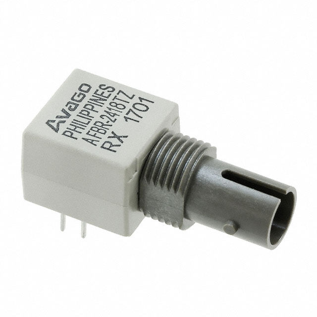
ICGOO电子元器件商城为您提供HFBR-2526Z由Avago Technologies设计生产,在icgoo商城现货销售,并且可以通过原厂、代理商等渠道进行代购。 HFBR-2526Z价格参考。Avago TechnologiesHFBR-2526Z封装/规格:光纤 - 接收器, Fiber Optic Receiver General Purpose -9.4dBm 0.8 V ~ 2.6 V 15mA。您可以下载HFBR-2526Z参考资料、Datasheet数据手册功能说明书,资料中有HFBR-2526Z 详细功能的应用电路图电压和使用方法及教程。
Broadcom Limited的HFBR-2526Z是一款光纤接收器,属于其光通信产品线。该器件主要用于将接收到的光信号转换为电信号,适用于高速光纤通信系统。

应用场景包括:

1. 工业自动化与控制:HFBR-2526Z常用于工业现场总线系统(如PROFIBUS、DeviceNet等),实现设备间高速、可靠的光信号传输,提升抗电磁干扰能力。

2. 通信设备:在光模块、交换机、路由器等网络设备中作为光接收单元,支持数据通信中的光电转换功能,适用于局域网(LAN)、广域网(WAN)等场景。

3. 医疗设备:用于需要电气隔离和高信号完整性的医疗监测与诊断设备中,保障设备安全与稳定运行。

4. 测试与测量仪器:在光纤测试设备中用作接收端组件,用于评估光链路性能,如光功率测试、误码率分析等。

5. 航空航天与军事:因具备高可靠性与稳定性,也适用于对环境适应性要求高的特殊领域,如雷达系统、飞行控制系统等。

该器件采用TTL电平输出,搭配对应的光发射器(如HFBR-1526Z)使用,构成完整的光纤收发方案,适合中短距离、高速率的数据传输应用。
| 参数 | 数值 |
| 产品目录 | |
| 描述 | 125MBD 650NM RECEIVER IN HORIZ光纤发射器、接收器、收发器 HI Speed V-Link Rx Horiz RoHS |
| 产品分类 | |
| 品牌 | Avago Technologies |
| 产品手册 | http://www.avagotech.com/pages/en/optical_receivers/general_purpose_industrial_control_data_link_650nm/hfbr-2526z/ |
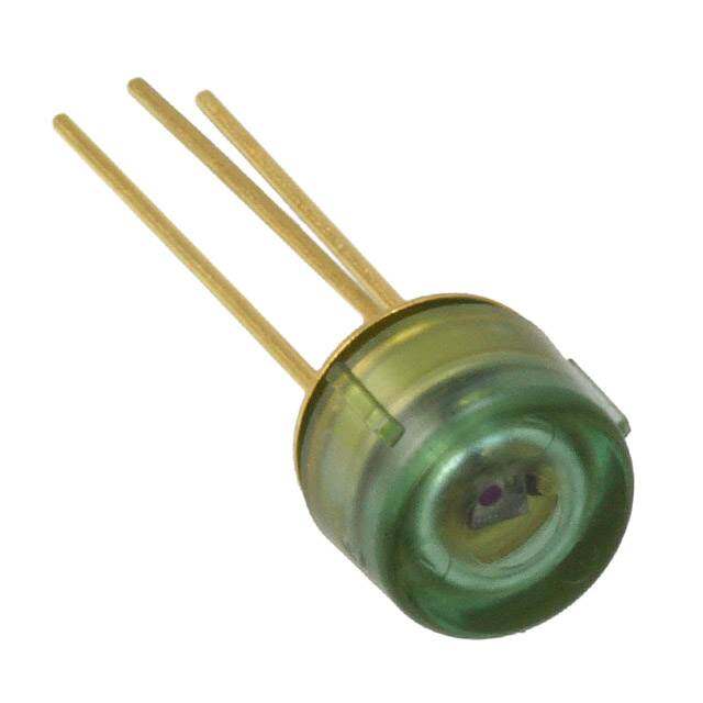
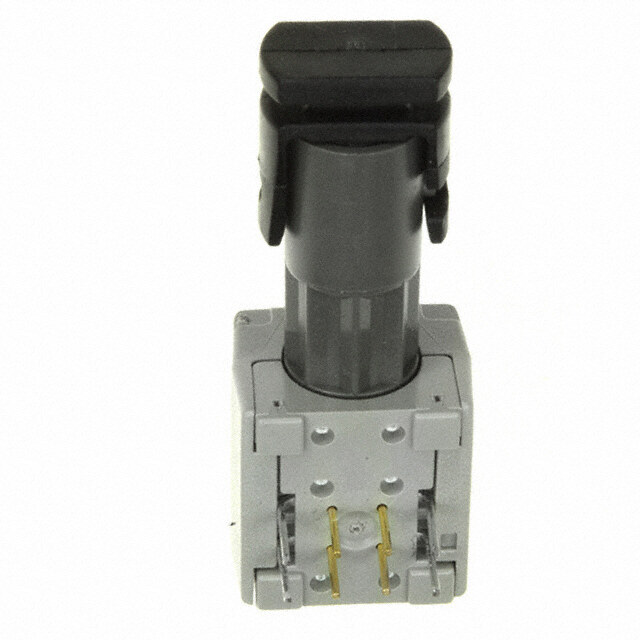
| 产品图片 |
|
| rohs | 符合RoHS无铅 / 符合限制有害物质指令(RoHS)规范要求 |
| 产品系列 | 光纤发射器、接收器、收发器,Avago Technologies HFBR-2526Z- |
| 数据手册 | http://www.avagotech.com/docs/AV02-1502EN |
| 产品型号 | HFBR-2526Z |
| PCN设计/规格 | http://www.avagotech.com/docs/V11-016-E47540-MA |
| 产品 | Receivers |
| 产品目录页面 | |
| 产品种类 | 光纤发射器、接收器、收发器 |
| 其它名称 | 516-1747 |
| 功率-可接受的最小值 | -9.4dBm |
| 商标 | Avago Technologies |
| 封装 | Tube |
| 封装/箱体 | - |
| 工作电源电压 | 5 V |
| 工厂包装数量 | 200 |
| 应用 | Industrial |
| 数据速率 | 1 MBd, 125 MBd |
| 最大工作温度 | + 70 C |
| 最大输出电流 | 25 mA |
| 最小工作温度 | 0 C |
| 标准包装 | 200 |
| 波长 | 650 nm |
| 电压-电源 | 0.8 V ~ 2.6 V |
| 电流-电源 | 15mA |
| 纤维类型 | Hard Clad Silica |


- 商务部:美国ITC正式对集成电路等产品启动337调查
- 曝三星4nm工艺存在良率问题 高通将骁龙8 Gen1或转产台积电
- 太阳诱电将投资9.5亿元在常州建新厂生产MLCC 预计2023年完工
- 英特尔发布欧洲新工厂建设计划 深化IDM 2.0 战略
- 台积电先进制程称霸业界 有大客户加持明年业绩稳了
- 达到5530亿美元!SIA预计今年全球半导体销售额将创下新高
- 英特尔拟将自动驾驶子公司Mobileye上市 估值或超500亿美元
- 三星加码芯片和SET,合并消费电子和移动部门,撤换高东真等 CEO
- 三星电子宣布重大人事变动 还合并消费电子和移动部门
- 海关总署:前11个月进口集成电路产品价值2.52万亿元 增长14.8%

PDF Datasheet 数据手册内容提取
HFBR-0507Z Series HFBR-15X7Z Transmitters HFBR-25X6Z Receivers 125 Megabaud Versatile Link The Versatile Fiber Optic Connection Data Sheet Description Features The 125 MBd Versatile Link (HFBR-0507Z Series) is the RoHS-compliant most cost-eff ective fi ber-optic solution for transmission Data transmission at signal rates of 1 to 125 MBd over of 125 MBd data over 100 meters. The data link consists distances of 100 meters of a 650 nm LED transmitter, HFBR-15X7Z, and a PIN/pre- Compatible with inexpen sive, easily terminated plas- amp receiver, HFBR-25X6Z. These can be used with low- tic optical fi ber, and with large core silica fi ber cost plastic or silica fi ber. One mm diameter plastic fi ber High voltage isolation provides the lowest cost solution for distances under 25 meters. The lower attenuation of silica fi ber allows data Transmitter and receiver application circuit transmission over longer distance, for a small diff erence schem atics and recommended board layouts avail- in cost. These com po nents can be used for high speed able data links without the problems common with copper Interlocking feature for single channel or duplex links, wire solutions, at a competitive cost. in a vertical or horizontal mount confi guration The HFBR-15X7Z transmitter is a high power 650 nm LED in a low cost plastic housing designed to effi ciently Applications couple power into 1 mm diameter plastic optical fi ber Intra-system links: board-to-board, rack-to-rack and 200 μm Hard Clad Silica (HCS®) fi ber. With the recom- Telecommunications switching systems mended drive circuit, the LED operates at speeds from 1-125 MBd. The HFBR-25X6Z is a high band width analog Computer-to-peripheral data links, PC bus extension receiver con tain ing a PIN photodiode and internal tran- Industrial control simpedance amplifi er. With the recommended applica- Proprietary LANs tion circuit for 125 MBd operation, the performance of Digitized video the complete data link is specifi ed for of 0-25 meters with plastic fi ber and 0-100 meters with 200 μm HCS® fi ber. A Medical instruments wide variety of other digitizing circuits can be combined Reduction of lightning and voltage transient suscepti- with the HFBR-0507Z Series to optimize perfor-mance bility and cost at higher and lower data rates. HCS® is a registered trademark of Spectran Corporation.
HFBR-0507Z Series 125 MBd Data Link Data link operating conditions and performance are operation. The Applications Engineer ing Department in specifi ed for the HFBR-15X7Z transmitter and HFBR-25X6Z the Avago Optical Communication Division is available to receiver in the recommended applications circuits shown assist in optimizing link performance for higher or lower in Figure 1. This circuit has been optimized for 125 MBd speed operation. Recommended Operating Conditions for the Circuits in Figures 1 and 2. Parameter Symbol Min. Max. Unit Reference Ambient Temperature T 0 70 °C A Supply Voltage V +4.75 +5.25 V CC Data Input Voltage – Low V V -1.89 V -1.62 V IL CC CC Data Input Voltage – High V V -1.06 V -0.70 V IH CC CC Data Output Load R 45 55 Ω Note 1 L Signaling Rate f 1 125 MBd S Duty Cycle D.C. 40 60 % Note 2 Link Performance: 1-125 MBd, BER ≤ 10-9, under recommended operating conditions with recommended transmit and receive application circuits. Parameter Symbol Min.[3] Typ.[4] Max. Unit Condition Reference Optical Power Budget, 1 m POF OPB 11 16 dB Note 5,6,7 POF Optical Power Margin, OPM 3 6 dB Note 5,6,7 POF,20 20 m Standard POF Link Distance with l 20 27 m Standard 1 mm POF Optical Power Margin, OPM 3 6 dB Note 5,6,7 POF,25 25 m Low Loss POF Link Distance with Extra l 25 32 m Low Loss 1 mm POF Optical Power Budget, 1 m HCS OPB 7 12 dB Note 5,6,7 HCS Optical Power Margin, OPM 3 6 dB Note 5,6,7 HCS,100 100 m HCS Link Distance with HCS Cable l 100 125 m Notes: 1. If the output of U4C in Figure 1, page 4 is transmitted via coaxial cable, terminate with a 50 Ω resistor to V - 2 V. CC 2. Run length limited code with maximum run length of 10 μs. 3. Minimum link performance is projected based on the worst case specifi cations of the HFBR-15X7Z transmitter, HFBR-25X6Z receiver, and POF cable, and the typical performance of other components (e.g. logic gates, transistors, resistors, capacitors, quantizer, HCS cable). 4. Typical performance is at 25°C, 125 MBd, and is measured with typical values of all circuit components. 5. Standard cable is HFBR-RXXYYYZ plastic optical fi ber , with a maximum attenuation of 0.24 dB/m at 650 nm and NA = 0.5. Extra low loss cable is HFBR-EXXYYYZ plastic optical fi ber, with a maximum attenuation of 0.19 dB/m at 650 nm and NA = 0.5. HCS cable is HFBR-H/VXXYYY glass optical fi ber, with a maximum attenuation of 10 dB/km at 650 nm and NA = 0.37. 6. Optical Power Budget is the diff erence between the transmitter output power and the receiver sensitivity, measured after 1 meter of fi ber. The minimum OPB is based on the limits of optical component performance over temperature, process, and recommended power supply variation. 7. The Optical Power Margin is the available OPB after including the eff ects of attenuation and modal dispersion for the minimum link distance: OPM = OPB - (attenuation power loss + modal dispersion power penalty). The minimum OPM is the margin available for longterm LED LOP degradation and additional fi xed passive losses (such as in-line connectors) in addition to the minimum specifi ed distance. 2
Plastic Optical Fiber (1 mm POF) Transmitter Application Circuit: Performance of the HFBR-15X7Z transmitter in the recom- mended application circuit (Figure 1) for POF; 1-125 MBd, 25°C. Parameter Symbol Typical Unit Condition Note Average Optical Power 1 mm POF P -9.7 dBm 50% Duty Note 1, Fig 3 avg Cycle Average Modulated Power 1 mm POF P -11.3 dBm Note 2, Fig 3 mod Optical Rise Time (10% to 90%) t 2.1 ns 5 MHz r Optical Fall Time (90% to 10%) t 2.8 ns 5 MHz f High Level LED Current (On) I 19 mA Note 3 F,H Low Level LED Current (Off ) I 3 mA Note 3 F,L Optical Overshoot - 1 mm POF 45 % Transmitter Application Circuit I 110 mA Figure 1 CC Current Consumption - 1 mm POF Hard Clad Silica Fiber (200 μm HCS) Transmitter Application Circuit: Performance of the HFBR-15X7Z transmitter in the recom- mended application circuit (Figure 1) for HCS; 1-125 MBd, 25°C. Parameter Symbol Typical Unit Condition Note Average Optical Power 200 μm HCS P -14.6 dBm 50% Duty Note 1, Fig 3 avg Cycle Average Modulated Power 200 μm HCS P -16.2 dBm Note 2, Fig 3 mod Optical Rise Time (10% to 90%) t 3.1 ns 5 MHz r Optical Fall Time (90% to 10%) t 3.4 ns 5 MHz f High Level LED Current (On) I 60 mA Note 3 F,H Low Level LED Current (Off ) I 6 mA Note 3 F,L Optical Overshoot - 200 μm HCS 30 % Transmitter Application Circuit I 130 mA Figure 1 CC Current Consumption - 200 μm HCS Notes: 1. Average optical power is measured with an average power meter at 50% duty cycle, after 1 meter of fi ber. 2. To allow the LED to switch at high speeds, the recommended drive circuit modulates LED light output between two non-zero power levels. The modulated (useful) power is the diff erence between the high and low level of light output power (transmitted) or input power (received), which can be measured with an average power meter as a function of duty cycle (see Figure 3). Average Modulated Power is defi ned as one half the slope of the average power versus duty cycle: [P @ 80% duty cycle - P @ 20% duty cycle] Average Modulated Power = avg avg (2) [0.80 - 0.20] 3. High and low level LED currents refer to the current through the HFBR-15X7Z LED. The low level LED “off ” current, sometimes referred to as “hold-on” current, is prebias supplied to the LED during the off state to facilitate fast switching speeds. 3
Plastic and Hard Clad Silica Optical Fiber Receiver Application Circuit: Performance[4] of the HFBR-25X6Z receiver in the recom- mended application circuit (Figure 1); 1-125 MBd, 25°C unless otherwise stated. Parameter Symbol Typical Unit Condition Note Data Output Voltage - Low V V -1.7 V R = 50 Ω Note 5 OL CC L Data Output Voltage - High V V -0.9 V R = 50 Ω Note 5 OH CC L Receiver Sensitivity to Average P -27.5 dBm 50% eye opening Note 2 min Modulated Optical Power 1 mm POF Receiver Sensitivity to Average P -28.5 dBm 50% eye opening Note 2 min Modulated Optical Power 200 μm HCS Receiver Overdrive Level of Average P -7.5 dBm 50% eye opening Note 2 max Modulated Optical Power 1 mm POF Receiver Overdrive Level of Average P -10.5 dBm 50% eye opening Note 2 max Modulated Optical Power 200 μm HCS Receiver Application Circuit Current I 85 mA R = ∞ Figure 1 CC L Consumption Notes: 4. Performance in response to a signal from the HFBR-15X7Z transmitter driven with the recommended circuit at 1-125 MBd over 1 meter of HFBR-RZ/EXXYYYZ plastic optical fi ber or 1 meter of HFBR-H/VXXYYY hard clad silica optical fi ber. 5. Terminated through a 50 Ω resistor to V - 2 V. CC 6. If there is no input optical power to the receiver, electrical noise can result in false triggering of the receiver. In typical applications, data encod- ing and error detection prevent random triggering from being interpreted as valid data. Refer to Applications Note 1066 for design guidelines. L1 CB70-1812 VCC 0.C0101 R5 0C.21 14 0C.31 0.C0401 C105 + 0C.61 0.C0701 22 9 8 8 10 U1C 1 7 74ACTQ00 R8* 23 U2 4 QBF1Q52 QBF2Q52 12 U1A 3 1132 7U41ADCTQ1010 2NQ39304 R9* 5HFBR-15X7Z 74ACTQ00 R916 R917 45 U1B 6 98QTX2 VBEAESE 74ACTQ00 C8* R1150 R11* J17654321QTRPPRNXIIXXC1NN VVVB 11CCEA98CECS 11E00HH111166 C1200 + C01.19 VBB 3V VCC C01.10 R41.72 .C497 AAW(ULRINTLELH CEI N1AS 0PMS%A IOC CTTROITHOLOE EFRRRA WVARAINASLCDEUE SNE,OSTED). C17 ALL RESISTANCES ARE IN R22 0.1 VBB OHMS WITH 5% TOLERANCE R24 1K R13 (UNLESS OTHERWISE NOTED). 1K R18 R16 4.7 1M8C10H116FN15 C01.16 5M1C104H11106FN 7 51MC109H11146FN 13 R11K4 C01.12 1 8 19 U4C 17 3 U4A 5 8 U4B 12 23 U3 C01.15 R5119 20 2 R5117 R11K5 C01.11 4 5 HFBR-25X6Z R12K5 R12K3 R20 VCC 3 V THE VALUES OF R8, R9, R11, AND VBB 12 VBB CH8C SA RDER IDVIEF FCEIRRCEUNITT SFO.R POF AND C01.18 R6221 U5 +C1104 C01.13 RRR8911 P33 100OK00F H 4 887C220S T O L E111R%%%ANCE TL431 C8 43 pF 120 pF 1% Figure 1. Transmitter and receiver application circuit with +5 V ECL inputs and outputs. 4
120 120 +5 V ECL SERIAL DATA SOURCE 82 0.1 μF 82 9 TX VEE 8 TD + 5 V Ð 7 TD 4.7 μH + 10 μF 0.1 μF 6 TX VCC 0.1 μF 5 RX VCC 10 μF 0.1 μF 82 82 + 4.7 μH 4 FIBER-OPTIC +5 V ECL 3 RD TSHRAONWSNC EINIV ER SERIAL DATA FIGURE 1 RECEIVER 2 RD 120 120 4.7 μH 1 RX VEE Figure 2. Recommended power supply fi lter and +5 V ECL signal terminations for the transmitter and receiver applica- tion circuit of Figure 1. 200 21 POF 19 W 150 dB Ð μ T Ð 17 GE R D WE 100 BU 15 O R AVERAGE P 50 AAMPVOVEOREWDRAEUAGRLGEA EPTOEDWER, OPTICAL POWE 1113 HCS 50% DUTY CYCLE 0 9 0 20 40 60 80 100 10 30 50 70 90 110 130 150 DUTY CYCLE Ð % DATA RATE Ð MBd Figure 3. Average modulated power. Figure 4. Typical optical power budget vs. data rate. 5
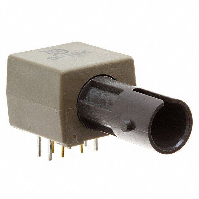
125 Megabaud Versatile Link Transmitter HFBR-15X7Z Series Description GROUND The HFBR-15X7Z transmitters incorporate a 650 nano- 1 ANODE meter LED in a horizontal (HFBR-1527Z) or vertical (HF- 2 CATHODE BR-1537Z) gray housing. The HFBR-15X7Z transmitters 3 GROUND are suitable for use with current peaking to decrease 4 GROUND response time and can be used with HFBR-25X6Z receiv- ers in data links operating at signal rates from 1 to 125 GROUND SEE NOTE 6 megabaud over 1 mm diameter plastic optical fi ber or 200 μm diameter hard clad silica glass optical fi ber. Refer to Applica tion Note 1066 for details for recom mended interface circuits. Absolute Maximum Ratings Parameter Symbol Min. Max. Unit Reference Storage Temperature T -40 85 °C S Operating Temperature T -40 70 °C O Lead Soldering Temperature Cycle Time 260 °C Note 1, 9 10 s Transmitter High Level Forward I 120 mA 50% Duty Cycle F,H Input Current ≥ 1 MHz Transmitter Average Forward Input Current I 60 mA F,AV Reverse Input Voltage V 3 V R CAUTION: The small junction sizes inherent to the design of this component increase the component’s suscep ti bility to damage from electrostatic discharge (ESD). It is advised that normal static precautions be taken in handling and assembly of this component to prevent damage and/or degradation which may be induced by ESD. WARNING: WHEN VIEWED UNDER SOME CONDITIONS, THE OPTICAL PORT MAY EXPOSE THE EYE BEYOND THE MAXI- MUM PERMISSIBLE EXPOSURE RECOMMENDED IN ANSI Z136.2, 1993. UNDER MOST VIEWING CONDITIONS THERE IS NO EYE HAZARD. 6
Electrical/Optical Characteristics 0 to 70°C, unless otherwise stated. Parameter Symbol Min. Typ.[2] Max. Unit Condition Note Transmitter Output P -9.5 -7.0 -4.8 dBm I = 20 mA, 25°C Note 3 T F,dc Optical Power, 1 mm POF -10.4 -4.3 0-70°C Transmitter Output P -6.0 -3.0 -0.5 dBm I = 60 mA, 25°C Note 3 T F,dc Optical Power, 1 mm POF -6.9 -0.0 0-70°C Transmitter Output P -14.6 -13.0 -10.5 dBm I = 60 mA, 25°C Note 3 T F,dc Optical Power, -15.5 -10.0 0-70°C 200 μm HCS® Output Optical Power ΔP -0.02 dB/°C T Temperature Coeffi cient ΔT Peak Emission Wavelength 640 650 660 nm PK Peak Wavelength Δ 0.12 nm/°C Temperature Coeffi cient ΔT Spectral Width FWHM 21 nm Full Width, Half Maximum Forward Voltage V 1.8 2.1 2.4 V I = 60 mA F F Forward Voltage ΔV -1.8 mV/°C F Temperature Coeffi cient ΔT Transmitter Numerical NA 0.5 Aperture Thermal Resistance, 140 °C/W Note 4 jc Junction to Case Reverse Input Breakdown V 3.0 13 V I = -10 μA BR F,dc Voltage Diode Capacitance C 60 pF V = 0 V, O F f = 1 MHz Unpeaked Optical Rise t 12 ns I = 60 mA Figure 1 r F Time, 10% - 90% f = 100 kHz Note 5 Unpeaked Optical Fall t 9 ns I = 60 mA Figure 1 f F Time, 90% - 10% f = 100 kHz Note 5 Notes: 1. 1.6 mm below seating plane. 2. Typical data is at 25°C. 3. Optical Power measured at the end of 0.5 meter of 1 mm diameter plastic or 200 μm diameter hard clad silica optical fi ber with a large area detector. 4. Typical value measured from junction to PC board solder joint for horizontal mount package, HFBR-1527Z. is approximately jc 30°C/W higher for vertical mount package, HFBR-1537Z. 5. Optical rise and fall times can be reduced with the appropriate driver circuit; refer to Application Note 1066. 6. Pins 5 and 8 are primarily for mounting and retaining purposes, but are electrically connected; pins 3 and 4 are electrically unconnected. It is recommended that pins 3, 4, 5, and 8 all be connected to ground to reduce coupling of electrical noise. 7. Refer to the Versatile Link Family Fiber Optic Cable and Connectors Technical Data Sheet for cable connector options for 1 mm plastic optical fi ber and 200 μm HCS fi ber. 8. The LED current peaking necessary for high frequency circuit design contributes to electromagnetic interference (EMI). Care must be taken in circuit board layout to minimize emissions for compliance with governmental EMI emissions regulations. Refer to Application Note 1066 for design guidelines. 9. Moisture sensitivity level (MSL) is 3 7
1.2 ER 0° C W O 1.0 P UT 25° C P HP8082A T 0.8 PULSE BCP MODEL 300 OU GENERATOR 500 MHz L 70° C BANDWIDTH RA 0.6 SILICON CT AVALANCHE E PHOTODIODE SP 0.4 D E Z 5L0O OAHDM 50H PO5H4M00 B2NAC OSCHIPL5L4O1S0C0AOPE RMALI 0.2 RESISTOR INPUT POD O N 0 620 630 640 650 660 670 680 WAVELENGTH (nm) Figure 1. Test circuit for measuring unpeaked rise and Figure 2. Typical spectra normalized to the 25°C peak. fall times. 2.4 0 B d LTAGE - V 2.2 72005° °°C CC UT POWER - -1-50 0° C O P WARD V 2.0 ED OUT -15 V - FORF 1.8 NORMALIZ -20 7205°° CC - T P 1.6 -25 1 10 100 1 10 100 IF,DC - TRANSMITTER DRIVE CURRENT (mA) IF,DC - TRANSMITTER DRIVE CURRENT (mA) Figure 3. Typical forward voltage vs. drive current. Figure 4. Typical normalized output optical power vs. drive current. 8
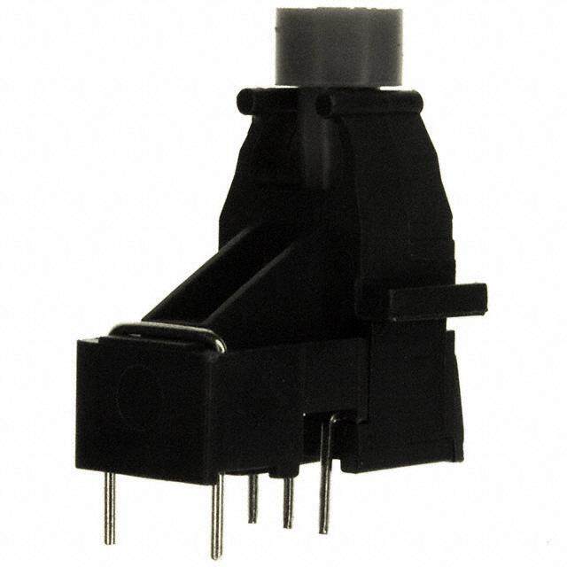
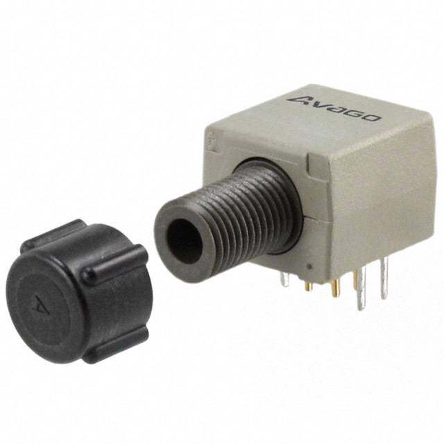
125 Megabaud Versatile Link Receiver HFBR-25X6Z Series Description The HFBR-25X6Z receivers contain a PIN photodiode and transimpedance pre-amplifi er circuit in a horizontal (HF- GROUND BR-2526Z) or vertical (HFBR-2536Z) blue housing, and 4 VCC are designed to interface to 1mm diameter plastic opti- GROUND 3 cal fi ber or 200 μm hard clad silica glass optical fi ber. The GROUND receivers convert a received optical signal to an analog 2 SIGNAL 1 output voltage. Follow-on circuitry can optimize link per- GROUND formance for a variety of distance and data rate require- SEE NOTES 2, 4, 9 ments. Electrical bandwidth greater than 65 MHz allows design of high speed data links with plastic or hard clad silica optical fi ber. Refer to Applica tion Note 1066 for de- tails for recommended interface circuits. Absolute Maximum Ratings Parameter Symbol Min. Max. Unit Reference Storage Temperature T -40 +75 °C S Operating Temperature T 0 +70 °C A Lead Soldering Temperature 260 °C Note 1, 11 Cycle Time 10 s Signal Pin Voltage V -0.5 V V O CC Supply Voltage V -0.5 6.0 V CC Output Current I 25 mA O CAUTION: The small junction sizes inherent to the design of this component increase the component’s suscep ti bility to damage from electrostatic discharge (ESD). It is advised that normal static precautions be taken in handling and assembly of this component to prevent damage and/or degradation which may be induced by ESD. 9
Electrical/Optical Characteristics 0 to 70°C; 5.25 V ≥ V ≥ 4.75 V; power supply must be fi ltered (see Figure 1, Note 2). CC Parameter Symbol Min. Typ. Max. Unit Test Condition Note AC Responsivity 1 mm POF R 1.7 3.9 6.5 mV/μW 650 nm Note 4 P,APF AC Responsivity 200 μm HCS R 4.5 7.9 11.5 mV/μW P,HCS RMS Output Noise V 0.46 0.69 mV Note 5 NO RMS Equivalent Optical Noise Input P - 39 -36 dBm Note 5 N,RMS Power, RMS - 1 mm POF Equivalent Optical Noise Input P -42 -40 dBm Note 5 N,RMS Power, RMS - 200 μm HCS Peak Input Optical Power - P -5.8 dBm 5 ns PWD Note 6 R 1 mm POF -6.4 dBm 2 ns PWD Peak Input Optical Power - P -8.8 dBm 5 ns PWD Note 6 R 200 μm HCS -9.4 dBm 2 ns PWD Output Impedance Z 30 Ω 50 MHz Note 4 O DC Output Voltage V 0.8 1.8 2.6 V P = 0 μW O R Supply Current I 9 15 mA CC Electrical Bandwidth BW 65 125 MHz -3 dB electrical E Bandwidth * Rise Time 0.41 Hz * s Electrical Rise Time, 10-90% t 3.3 6.3 ns P = -10 dBm r R peak Electrical Fall Time, 90-10% t 3.3 6.3 ns P = -10 dBm f R peak Pulse Width Distortion PWD 0.4 1.0 ns P = -10 dBm Note 7 R peak Overshoot 4 % P = -10 dBm Note 8 R peak Notes: 1. 1.6 mm below seating plane. 2. The signal output is an emitter follower, which does not reject noise in the power supply. The power supply must be fi ltered as in Figure 1. 3. Typical data are at 25°C and V = +5 Vdc. CC 4. Pin 1 should be ac coupled to a load ≥ 510 Ω with load capacitance less than 5 pF. 5. Measured with a 3 pole Bessel fi lter with a 75 MHz, -3dB bandwidth. 6. The maximum Peak Input Optical Power is the level at which the Pulse Width Distortion is guaranteed to be less than the PWD listed under Test Condition. P is given for PWD = 5 ns for designing links at ≤ 50 MBd operation, and also for PWD = 2 ns for designing links up to 125 R,Max MBd (for both POF and HCS input conditions). 7. 10 ns pulse width, 50% duty cycle, at the 50% amplitude point of the waveform. 8. Percent overshoot is defi ned at: (V - V ) –––P–K–––1–00–%––– 100% V 100% 9. Pins 5 and 8 are primarily for mounting and retaining purposes, but are electrically connected. It is recommended that these pins be con- nected to ground to reduce coupling of electrical noise. 10. If there is no input optical power to the receiver (no transmitted signal) electrical noise can result in false triggering of the receiver. In typical applications, data encoding and error detection prevent random triggering from being interpreted as valid data. Refer to Application Note 1066 for design guidelines. 11. Moisture sensitivity level (MSL) is 4 10
Figure 1. Recommended power supply fi lter circuit. Figure 2. Simplifi ed receiver schematic. Figure 3. Typical pulse width distortion vs. peak input Figure 4. Typical output spectral noise density vs. Figure 5. Typical rise and fall time vs. temperature. power. frequency. 11
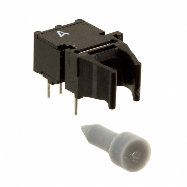
Versatile Link Mechanical Dimensions HORIZONTAL MODULES HORIZONTAL MODULES HFBR-1527Z HFBR-1537Z HFBR-2526Z HFBR-2526Z 5.08 2.03 6.86 10.16 (0.200) (0.080) (0.270) 2.03 (0.400) 10.16 (0.080) (0.400) 18.8 5.08 18.29 (0.74) (0.200) 6.86 (0.720) (0.27) 4.19 0.64 7.62 (0.165) (0.025) (0.30) 18.80 (0.740) 3.81 (0.150) MAX. 7.62 3.56 (0.140) MIN. 1.27 (0.300) 0.51 (0.050) (0.020) 2.54 (0.100) 0.64 (0.025) DIA. 2.77 1.85 (0.109) (0.073) Versatile Link Printed Circuit Board Layout Dimensions TOP VIEWS HORIZONTAL MODULE VERTICAL MODULE 7.62 (0.300) 2.54 (0.100) 1.01 (0.040) DIA. 4 3 2 1 TOP VIEW 7.62 (0.300) 5 8 PCB EDGE 1.85 MIN. (0.073) DIMENSIONS IN MILLIMETERS (INCHES). For product information and a complete list of distributors, please go to our website: www.avagotech.com Avago, Avago Technologies, and the A logo are trademarks of Avago Technologies in the United States and other countries. Data subject to change. Copyright © 2005-2012 Avago Technologies. All rights reserved. Obsoletes 5989-4631EN AV02-1502EN - April 11, 2012
Mouser Electronics Authorized Distributor Click to View Pricing, Inventory, Delivery & Lifecycle Information: B roadcom Limited: HFBR-1517Z HFBR-1527Z HFBR-1537Z HFBR-2526Z HFBR-2536Z