
 Datasheet下载
- 型号: HEF4044BT,653
- 制造商: NXP Semiconductors
- 库位|库存: xxxx|xxxx
- 要求:
| 数量阶梯 | 香港交货 | 国内含税 |
| +xxxx | $xxxx | ¥xxxx |
查看当月历史价格
查看今年历史价格
HEF4044BT,653产品简介:
ICGOO电子元器件商城为您提供HEF4044BT,653由NXP Semiconductors设计生产,在icgoo商城现货销售,并且可以通过原厂、代理商等渠道进行代购。 HEF4044BT,653价格参考。NXP SemiconductorsHEF4044BT,653封装/规格:逻辑 - 锁销, S-R Latch 4 Channel 4:4 IC Tri-State 16-SO。您可以下载HEF4044BT,653参考资料、Datasheet数据手册功能说明书,资料中有HEF4044BT,653 详细功能的应用电路图电压和使用方法及教程。
HEF4044BT,653 是由 NXP USA Inc. 生产的逻辑电路,属于锁存器(锁销)类别。这种器件主要用于数字信号处理和存储应用中,能够实现数据的临时保存与传输控制。具体来说,HEF4044BT,653 是一个四通道透明 D 型锁存器,具有以下应用场景:

1. 数据缓冲与同步:在多路复用系统或需要对多个输入信号进行同步处理的应用中,HEF4044BT,653 可以用于暂时存储输入数据,并在适当的时钟信号触发下将数据传递到下一个阶段。这有助于确保数据的一致性和完整性。

2. 通信接口设计:在串行通信协议(如 UART、SPI 等)中,锁存器可以用来保持数据稳定,防止数据在传输过程中发生竞争冒险现象。HEF4044BT,653 的透明特性使其能够在时钟信号高电平时直接传递输入信号,在低电平时锁定当前状态,从而确保数据的准确传输。

3. 工业控制系统:在自动化设备和工业控制系统中,锁存器常用于输入/输出端口扩展。例如,当需要同时读取多个传感器的状态或将控制命令发送到多个执行机构时,HEF4044BT,653 可以帮助管理这些并行操作,提高系统的响应速度和可靠性。

4. 音频和视频处理:在多媒体设备中,锁存器可用于同步音频和视频信号的采样率转换。通过精确控制数据流的时间点,可以避免因不同模块之间的工作频率差异而导致的失真问题。

5. 消费电子产品:在一些消费类电子产品中,如键盘、鼠标等外设,HEF4044BT,653 也可以用于处理按键扫描矩阵中的信号,确保每次按键操作都能被正确识别并传递给主控芯片。

总之,HEF4044BT,653 作为一款高性能的逻辑锁存器,在各种需要数据暂存、同步及传输控制的应用场景中发挥着重要作用。
| 参数 | 数值 |
| 产品目录 | 集成电路 (IC)半导体 |
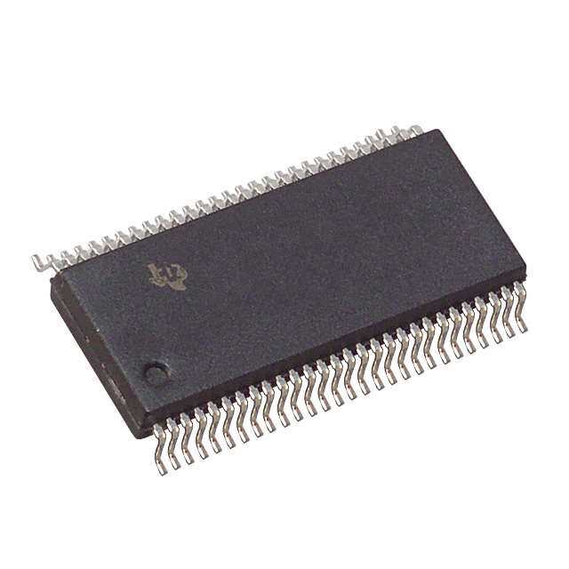
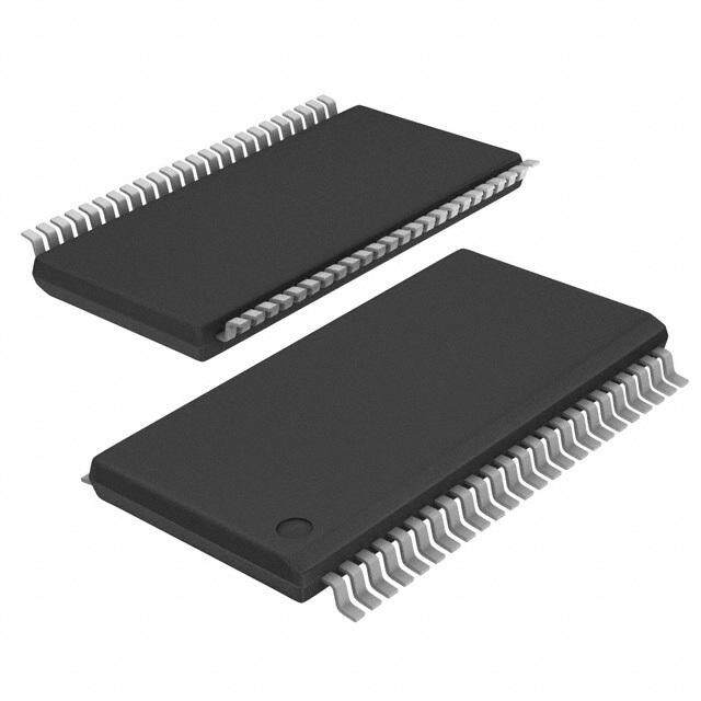
| 描述 | IC R/S LATCH 3-STATE QUAD 16SOIC闭锁 QUAD R/S LATCH W/3-STATE OUTPT |
| 产品分类 | |
| 品牌 | NXP Semiconductors |
| 产品手册 | |
| 产品图片 |
|
| rohs | 符合RoHS无铅 / 符合限制有害物质指令(RoHS)规范要求 |
| 产品系列 | 逻辑集成电路,闭锁,NXP Semiconductors HEF4044BT,6534000B |
| 数据手册 | |
| 产品型号 | HEF4044BT,653 |
| PCN封装 | |
| PCN组件/产地 | |
| 产品种类 | 闭锁 |
| 传播延迟时间 | 30 ns at 15 V |
| 低电平输出电流 | 32 mA |
| 供应商器件封装 | 16-SO |
| 其它名称 | 568-8230-6 |
| 包装 | Digi-Reel® |
| 商标 | NXP Semiconductors |
| 安装类型 | 表面贴装 |
| 安装风格 | SMD/SMT |
| 封装 | Reel |
| 封装/外壳 | 16-SOIC(0.154",3.90mm 宽) |
| 封装/箱体 | SO-16 |
| 工作温度 | -40°C ~ 85°C |
| 工厂包装数量 | 2500 |
| 延迟时间-传播 | 30ns |
| 最大工作温度 | + 85 C |
| 最小工作温度 | - 40 C |
| 极性 | Non-Inverting |
| 标准包装 | 1 |
| 独立电路 | 4 |
| 电压-电源 | 3 V ~ 15 V |
| 电流-输出高,低 | 3mA,3mA |
| 电源电压-最大 | 15.5 V |
| 电源电压-最小 | 4.5 V |
| 电路 | 4:4 |
| 电路数量 | 4 Circuit |
| 输入线路数量 | 8 Line |
| 输出类型 | 三态 |
| 输出线路数量 | 4 Line |
| 逻辑类型 | S-R 锁存器 |
| 逻辑系列 | HEF4000 |
| 零件号别名 | HEF4044BTD-T |
| 高电平输出电流 | - 3.6 mA |


- 商务部:美国ITC正式对集成电路等产品启动337调查
- 曝三星4nm工艺存在良率问题 高通将骁龙8 Gen1或转产台积电
- 太阳诱电将投资9.5亿元在常州建新厂生产MLCC 预计2023年完工
- 英特尔发布欧洲新工厂建设计划 深化IDM 2.0 战略
- 台积电先进制程称霸业界 有大客户加持明年业绩稳了
- 达到5530亿美元!SIA预计今年全球半导体销售额将创下新高
- 英特尔拟将自动驾驶子公司Mobileye上市 估值或超500亿美元
- 三星加码芯片和SET,合并消费电子和移动部门,撤换高东真等 CEO
- 三星电子宣布重大人事变动 还合并消费电子和移动部门
- 海关总署:前11个月进口集成电路产品价值2.52万亿元 增长14.8%


PDF Datasheet 数据手册内容提取
HEF4044B Quad R/S latch with 3-state outputs Rev. 10 — 18 November 2011 Product data sheet 1. General description The HEF4044B is a quad R/S latch with 3-state outputs, with a common output enable input (OE). Each latch has an active LOW set input (1S to 4S), an active LOW reset input (1R to 4R) and an active HIGH 3-state output (1Qto 4Q). When OE is HIGH, the latch output (nQ) is determined by the nR and nS inputs as shown in Table3. When OE is LOW, the latch outputs are in the high impedance OFF-state. OE does not affect the state of the latch. The high impedance off-state feature allows common bussing of the outputs. It operates over a recommended V power supply range of 3V to 15 V referenced to V DD SS (usually ground). Unused inputs must be connected to V , V , or another input. DD SS 2. Features and benefits Fully static operation 5 V, 10 V, and 15 V parametric ratings Standardized symmetrical output characteristics Specified from 40 C to +85 C Complies with JEDEC standard JESD 13-B 3. Applications Four-bit storage with output enable 4. Ordering information Table 1. Ordering info rmation All types operate from 40C to +85C. Type number Package Name Description Version HEF4044BP DIP16 plastic dual in-line package; 16 leads (300 mil) SOT38-4 HEF4044BT SO16 plastic small outline package; 16 leads; body width 3.9mm SOT109-1
HEF4044B NXP Semiconductors Quad R/S latch with 3-state outputs 5. Functional diagram 3 1S 1Q 13 4 1R 7 2S 2Q 9 6 2R nS 3-STATE 11 3S OUTPUTS 3Q 10 12 3R nQ nR 15 4S 4Q 1 14 4R OE 5 OE to other latches 001aae621 001aai542 Fig 1. Functional diagram Fig 2. Logic diagram for one latch 6. Pinning information 6.1 Pinning HEF4044B 4Q 1 16 VDD n.c. 2 15 4S 1S 3 14 4R 1R 4 13 1Q OE 5 12 3R 2R 6 11 3S 2S 7 10 3Q VSS 8 9 2Q 001aae622 Fig 3. Pin configuration HEF4044B All information provided in this document is subject to legal disclaimers. © NXP B.V. 2011. All rights reserved. Product data sheet Rev. 10 — 18 November 2011 2 of 14
HEF4044B NXP Semiconductors Quad R/S latch with 3-state outputs 6.2 Pin description Table 2. Pin descripti on Symbol Pin Description n.c. 2 not connected 1S to 4S 3, 7, 11, 15 set input (active LOW) 1R to 4R 4, 6, 12, 14 reset input (active LOW) OE 5 common output enable input V 8 ground supply voltage SS 1Q to 4Q 13, 9, 10, 1 3-state buffered latch output V 16 supply voltage DD 7. Functional description Table 3. Function tab le[1] Input Output OE nS nR nQ L X X Z H L H H H X L L H H H latched [1] H = HIGH voltage level; L = LOW voltage level; X = don’t care; Z = high impedance state. 8. Limiting values Table 4. Limiting valu es In accordance with the Absolute Maximum Rating System (IEC 60134). Symbol Parameter Conditions Min Max Unit V supply voltage 0.5 +18 V DD I input clamping current V <0.5V or V >V + 0.5 V - 10 mA IK I I DD V input voltage 0.5 V + 0.5 V I DD I output clamping current V <0.5V or V >V + 0.5 V - 10 mA OK O O DD I input/output current - 10 mA I/O I supply current - 50 mA DD T storage temperature 65 +150 C stg T ambient temperature 40 +85 C amb P total power dissipation T 40 C to +85 C tot amb DIP16 package [1] - 750 mW SO16 package [2] - 500 mW per output - 100 mW [1] For DIP16 package: Ptot derates linearly with 12 mW/K above 70 C. [2] For SO16 package: Ptot derates linearly with 8 mW/K above 70 C. HEF4044B All information provided in this document is subject to legal disclaimers. © NXP B.V. 2011. All rights reserved. Product data sheet Rev. 10 — 18 November 2011 3 of 14
HEF4044B NXP Semiconductors Quad R/S latch with 3-state outputs 9. Recommended operating conditions Table 5. Recommend ed operating conditions Symbol Parameter Conditions Min Typ Max Unit V supply voltage 3 - 15 V DD V input voltage 0 - V V I DD T ambient temperature in free air 40 - +85 C amb t/V input transition rise and fall rate V = 5 V - - 3.75 s/V DD V = 10 V - - 0.5 s/V DD V = 15 V - - 0.08 s/V DD 10. Static characteristics Table 6. Static charac teristics V = 0 V; V = V or V unless otherwise specified. SS I SS DD Symbol Parameter Conditions V T = 40 C T = 25 C T = 85 C Unit DD amb amb amb Min Max Min Max Min Max V HIGH-level inputvoltage I < 1 A 5 V 3.5 - 3.5 - 3.5 - V IH O 10 V 7.0 - 7.0 - 7.0 - V 15 V 11.0 - 11.0 - 11.0 - V V LOW-level inputvoltage I < 1 A 5 V - 1.5 - 1.5 - 1.5 V IL O 10 V - 3.0 - 3.0 - 3.0 V 15 V - 4.0 - 4.0 - 4.0 V V HIGH-level outputvoltage I < 1 A 5 V 4.95 - 4.95 - 4.95 - V OH O 10 V 9.95 - 9.95 - 9.95 - V 15 V 14.95 - 14.95 - 14.95 - V V LOW-level output voltage I < 1 A 5 V - 0.05 - 0.05 - 0.05 V OL O 10 V - 0.05 - 0.05 - 0.05 V 15 V - 0.05 - 0.05 - 0.05 V I HIGH-level output current V = 2.5 V 5 V - 1.7 - 1.4 - 1.1 mA OH O V = 4.6 V 5 V - 0.52 - 0.44 - 0.36 mA O V = 9.5 V 10 V - 1.3 - 1.1 - 0.9 mA O V = 13.5 V 15 V - 3.6 - 3.0 - 2.4 mA O I LOW-level outputcurrent V = 0.4 V 5 V 0.52 - 0.44 - 0.36 - mA OL O V = 0.5 V 10 V 1.3 - 1.1 - 0.9 - mA O V = 1.5 V 15 V 3.6 - 3.0 - 2.4 - mA O I input leakage current 15 V - 0.3 - 0.3 - 1.0 A I I OFF-state output current nQ output HIGH; 15 V - 1.6 - 1.6 - 12.0 A OZ returned to V DD nQ output LOW; 15 V - 1.6 - 1.6 - 12.0 A returned to V SS HEF4044B All information provided in this document is subject to legal disclaimers. © NXP B.V. 2011. All rights reserved. Product data sheet Rev. 10 — 18 November 2011 4 of 14
HEF4044B NXP Semiconductors Quad R/S latch with 3-state outputs Table 6. Static characteristics …continued V = 0 V; V = V or V unless otherwise specified. SS I SS DD Symbol Parameter Conditions V T = 40 C T = 25 C T = 85 C Unit DD amb amb amb Min Max Min Max Min Max I supply current I = 0A 5 V - 20 - 20 - 150 A DD O 10 V - 40 - 40 - 300 A 15 V - 80 - 80 - 600 A C input capacitance - - - 7.5 - - pF I 11. Dynamic characteristics Table 7. Dynamic cha racteristics V = 0 V; T = 25 C; for test circuit see Figure6; unless otherwise specified. SS amb Symbol Parameter Conditions V Extrapolation formula Min Typ Max Unit DD t HIGH to LOW nRtonQ; see 5 V [1] 63 ns + (0.55 ns/pF)C - 90 185 ns PHL L propagation delay Figure4 10 V 29 ns + (0.23 ns/pF)C - 40 80 ns L 15 V 22 ns + (0.16 ns/pF)C - 30 60 ns L t LOW to HIGH nStonQ; 5 V [1] 63 ns + (0.55 ns/pF)C - 90 180 ns PLH L propagation delay seeFigure4 10 V 29 ns + (0.23 ns/pF)C - 40 80 ns L 15 V 22 ns + (0.16 ns/pF)C - 30 60 ns L t transition time see Figure4 5 V [1] 10 ns + (1.00 ns/pF)C - 60 120 ns t L 10 V 9 ns + (0.42 ns/pF)C - 30 60 ns L 15 V 6 ns + (0.28 ns/pF)C - 20 40 ns L t HIGH to OFF-state OE nQ; 5 V - 50 100 ns PHZ propagation delay seeFigure5 10 V - 30 60 ns 15 V - 25 50 ns t LOW to OFF-state OE nQ; 5 V - 30 60 ns PLZ propagation delay seeFigure5 10 V - 25 45 ns 15 V - 20 40 ns t OFF-state to HIGH OE nQ; 5 V - 50 100 ns PZH propagation delay seeFigure5 10 V - 25 50 ns 15 V - 20 40 ns t OFF-state to LOW OE nQ; 5 V - 50 95 ns PZL propagation delay seeFigure5 10 V - 25 45 ns 15 V - 20 35 ns t pulse width nS input LOW; 5 V 30 15 - ns W minimum width; 10 V 20 10 - ns see Figure4 15 V 16 8 - ns nR input LOW; 5 V 30 15 - ns minimum width; 10 V 20 10 - ns see Figure4 15 V 16 8 - ns [1] The typical values of the propagation delay and transition times are calculated from the extrapolation formulas shown (C in pF). L HEF4044B All information provided in this document is subject to legal disclaimers. © NXP B.V. 2011. All rights reserved. Product data sheet Rev. 10 — 18 November 2011 5 of 14
HEF4044B NXP Semiconductors Quad R/S latch with 3-state outputs Table 8. Dynamic pow er dissipation P D P can be calculated from the formulas shown. V = 0 V; t = t 20 ns; T = 25 C. D SS r f amb Symbol Parameter V Typical formula for P (W) where: DD D P dynamic power 5 V P = 1300 f + (f C ) V 2 f = input frequency in MHz, D D i o L DD i dissipation 10 V PD = 5200 fi + (fo CL) VDD2 fo = output frequency in MHz, 15 V PD = 12900 fi + (fo CL) VDD2 CL = output load capacitance in pF, V = supply voltage in V, DD (f C ) = sum of the outputs. o L 12. Waveforms tf tr VI 90 % input nS VM 10 % 0 V tW tW VI input nR VM 0 V tPLH tPHL VOH 90 % output nQ VM 10 % VOL tTLH tTHL 001aai543 Measurement points are given in Table9. Logic levels: VOL and VOH are typical output voltage levels that occur with the output load. Fig 4. Set (nS) and reset (nR) inputs pulse width and propagation delay to latch output (nQ) and outputnQtransitiontime HEF4044B All information provided in this document is subject to legal disclaimers. © NXP B.V. 2011. All rights reserved. Product data sheet Rev. 10 — 18 November 2011 6 of 14
HEF4044B NXP Semiconductors Quad R/S latch with 3-state outputs VDD OE input VSS tPLZ tPZL output VDD VY LOW-to-OFF OFF-to-LOW VSS VX tPHZ tPZH output VDD VY HIGH-to-OFF OFF-to-HIGH VSS VX outputs on outputs off outputs on 001aag355 Measurement points are given in Table9. Fig 5. Output enable (OE) to latch output (nQ) enable time (t and t ) and disable time (t and t ) PZL PZH PLZ PHZ Table 9. Measuremen t points Supply voltage Input Output V V V V V V DD I M M X Y 5 V to 15 V V or V 0.5V 0.5V 0.1V 0.9V DD SS DD DD DD DD HEF4044B All information provided in this document is subject to legal disclaimers. © NXP B.V. 2011. All rights reserved. Product data sheet Rev. 10 — 18 November 2011 7 of 14
HEF4044B NXP Semiconductors Quad R/S latch with 3-state outputs tW VI 90 % 90 % negative pulse VM VM 10 % 10 % 0 V tf tr tr tf VI 90 % 90 % positive pulse VM VM 10 % 10 % 0 V tW 001aaj781 a. Input waveform VEXT VDD RL VI VO G DUT RT CL 001aaj915 b. Test circuit Test and measurement data is given in Table10. Definitions test circuit: DUT = Device Under Test. RT = Termination resistance should be equal to output impedance Zo of the pulse generator. C = Load capacitance including jig and probe capacitance. L Fig 6. Test circuit for measuring switching times Table 10. Test data Supply voltage Input Load V EXT V t, t C R t , t t , t t , t I r f L L PLH PHL PLZ PZL PHZ PZH 5V to 15V V 20 ns 50pF 1 k open V GND DD DD HEF4044B All information provided in this document is subject to legal disclaimers. © NXP B.V. 2011. All rights reserved. Product data sheet Rev. 10 — 18 November 2011 8 of 14
HEF4044B NXP Semiconductors Quad R/S latch with 3-state outputs 13. Package outline DIP16: plastic dual in-line package; 16 leads (300 mil) SOT38-4 D ME e n a pl g n eati A2 A s L A1 c Z e w M b1 (e ) 1 b b2 16 9 MH pin 1 index E 1 8 0 5 10 mm scale DIMENSIONS (inch dimensions are derived from the original mm dimensions) UNIT mAax. mAi n1 . mAa 2x . b b1 b2 c D(1) E(1) e e1 L ME MH w mZa(1x). 1.73 0.53 1.25 0.36 19.50 6.48 3.60 8.25 10.0 mm 4.2 0.51 3.2 2.54 7.62 0.254 0.76 1.30 0.38 0.85 0.23 18.55 6.20 3.05 7.80 8.3 inches 0.17 0.02 0.13 0.068 0.021 0.049 0.014 0.77 0.26 0.1 0.3 0.14 0.32 0.39 0.01 0.03 0.051 0.015 0.033 0.009 0.73 0.24 0.12 0.31 0.33 Note 1. Plastic or metal protrusions of 0.25 mm (0.01 inch) maximum per side are not included. OUTLINE REFERENCES EUROPEAN ISSUE DATE VERSION IEC JEDEC JEITA PROJECTION 95-01-14 SOT38-4 03-02-13 Fig 7. Package outline SOT38-4 (DIP16) HEF4044B All information provided in this document is subject to legal disclaimers. © NXP B.V. 2011. All rights reserved. Product data sheet Rev. 10 — 18 November 2011 9 of 14
HEF4044B NXP Semiconductors Quad R/S latch with 3-state outputs SO16: plastic small outline package; 16 leads; body width 3.9 mm SOT109-1 D E A X c y HE v M A Z 16 9 Q A2 A1 (A 3 ) A pin 1 index θ Lp 1 8 L e w M detail X bp 0 2.5 5 mm scale DIMENSIONS (inch dimensions are derived from the original mm dimensions) A UNIT max. A1 A2 A3 bp c D(1) E(1) e HE L Lp Q v w y Z(1) θ 0.25 1.45 0.49 0.25 10.0 4.0 6.2 1.0 0.7 0.7 mm 1.75 0.25 1.27 1.05 0.25 0.25 0.1 0.10 1.25 0.36 0.19 9.8 3.8 5.8 0.4 0.6 0.3 8o 0.010 0.057 0.019 0.0100 0.39 0.16 0.244 0.039 0.028 0.028 0o inches 0.069 0.01 0.05 0.041 0.01 0.01 0.004 0.004 0.049 0.014 0.0075 0.38 0.15 0.228 0.016 0.020 0.012 Note 1. Plastic or metal protrusions of 0.15 mm (0.006 inch) maximum per side are not included. OUTLINE REFERENCES EUROPEAN ISSUE DATE VERSION IEC JEDEC JEITA PROJECTION 99-12-27 SOT109-1 076E07 MS-012 03-02-19 Fig 8. Package outline SOT109-1 (SO16) HEF4044B All information provided in this document is subject to legal disclaimers. © NXP B.V. 2011. All rights reserved. Product data sheet Rev. 10 — 18 November 2011 10 of 14
HEF4044B NXP Semiconductors Quad R/S latch with 3-state outputs 14. Revision history Table 11. Revision history Document ID Release date Data sheet status Change notice Supersedes HEF4044B v.10 20111118 Product data sheet - HEF4044B v.9 Modifications: • Table6: I minimumvalues changed to maximum OH HEF4044B v.9 20091215 Product data sheet - HEF4044B v.8 HEF4044B v.8 20091127 Product data sheet - HEF4044B v.7 HEF4044B v.7 20090721 Product data sheet - HEF4044B v.6 HEF4044B v.6 20081111 Product data sheet - HEF4044B v.5 HEF4044B v.5 20080812 Product data sheet - HEF4044B v.4 HEF4044B v.4 20080717 Product data sheet - HEF4044B_CNV v.3 HEF4044B_CNV v.3 19950101 Product specification - HEF4044B_CNV v.2 HEF4044B_CNV v.2 19950101 Product specification - - HEF4044B All information provided in this document is subject to legal disclaimers. © NXP B.V. 2011. All rights reserved. Product data sheet Rev. 10 — 18 November 2011 11 of 14
HEF4044B NXP Semiconductors Quad R/S latch with 3-state outputs 15. Legal information 15.1 Data sheet status Document status[1][2] Product status[3] Definition Objective [short] data sheet Development This document contains data from the objective specification for product development. Preliminary [short] data sheet Qualification This document contains data from the preliminary specification. Product [short] data sheet Production This document contains the product specification. [1] Please consult the most recently issued document before initiating or completing a design. [2] The term ‘short data sheet’ is explained in section “Definitions”. [3] The product status of device(s) described in this document may have changed since this document was published and may differ in case of multiple devices. The latest product status information is available on the Internet at URLhttp://www.nxp.com. 15.2 Definitions malfunction of an NXP Semiconductors product can reasonably be expected to result in personal injury, death or severe property or environmental damage. NXP Semiconductors accepts no liability for inclusion and/or use of Draft — The document is a draft version only. The content is still under NXP Semiconductors products in such equipment or applications and internal review and subject to formal approval, which may result in therefore such inclusion and/or use is at the customer’s own risk. modifications or additions. NXP Semiconductors does not give any representations or warranties as to the accuracy or completeness of Applications — Applications that are described herein for any of these information included herein and shall have no liability for the consequences of products are for illustrative purposes only. NXP Semiconductors makes no use of such information. representation or warranty that such applications will be suitable for the specified use without further testing or modification. Short data sheet — A short data sheet is an extract from a full data sheet with the same product type number(s) and title. A short data sheet is intended Customers are responsible for the design and operation of their applications for quick reference only and should not be relied upon to contain detailed and and products using NXP Semiconductors products, and NXP Semiconductors full information. For detailed and full information see the relevant full data accepts no liability for any assistance with applications or customer product sheet, which is available on request via the local NXP Semiconductors sales design. It is customer’s sole responsibility to determine whether the NXP office. In case of any inconsistency or conflict with the short data sheet, the Semiconductors product is suitable and fit for the customer’s applications and full data sheet shall prevail. products planned, as well as for the planned application and use of customer’s third party customer(s). Customers should provide appropriate Product specification — The information and data provided in a Product design and operating safeguards to minimize the risks associated with their data sheet shall define the specification of the product as agreed between applications and products. NXP Semiconductors and its customer, unless NXP Semiconductors and NXP Semiconductors does not accept any liability related to any default, customer have explicitly agreed otherwise in writing. In no event however, damage, costs or problem which is based on any weakness or default in the shall an agreement be valid in which the NXP Semiconductors product is customer’s applications or products, or the application or use by customer’s deemed to offer functions and qualities beyond those described in the third party customer(s). Customer is responsible for doing all necessary Product data sheet. testing for the customer’s applications and products using NXP Semiconductors products in order to avoid a default of the applications and 15.3 Disclaimers the products or of the application or use by customer’s third party customer(s). NXP does not accept any liability in this respect. Limited warranty and liability — Information in this document is believed to Limiting values — Stress above one or more limiting values (as defined in be accurate and reliable. However, NXP Semiconductors does not give any the Absolute Maximum Ratings System of IEC60134) will cause permanent representations or warranties, expressed or implied, as to the accuracy or damage to the device. Limiting values are stress ratings only and (proper) completeness of such information and shall have no liability for the operation of the device at these or any other conditions above those given in consequences of use of such information. the Recommended operating conditions section (if present) or the Characteristics sections of this document is not warranted. Constant or In no event shall NXP Semiconductors be liable for any indirect, incidental, repeated exposure to limiting values will permanently and irreversibly affect punitive, special or consequential damages (including - without limitation - lost the quality and reliability of the device. profits, lost savings, business interruption, costs related to the removal or replacement of any products or rework charges) whether or not such Terms and conditions of commercial sale — NXP Semiconductors damages are based on tort (including negligence), warranty, breach of products are sold subject to the general terms and conditions of commercial contract or any other legal theory. sale, as published at http://www.nxp.com/profile/terms, unless otherwise Notwithstanding any damages that customer might incur for any reason agreed in a valid written individual agreement. In case an individual whatsoever, NXP Semiconductors’ aggregate and cumulative liability towards agreement is concluded only the terms and conditions of the respective customer for the products described herein shall be limited in accordance agreement shall apply. NXP Semiconductors hereby expressly objects to with the Terms and conditions of commercial sale of NXP Semiconductors. applying the customer’s general terms and conditions with regard to the purchase of NXP Semiconductors products by customer. Right to make changes — NXP Semiconductors reserves the right to make changes to information published in this document, including without No offer to sell or license — Nothing in this document may be interpreted or limitation specifications and product descriptions, at any time and without construed as an offer to sell products that is open for acceptance or the grant, notice. This document supersedes and replaces all information supplied prior conveyance or implication of any license under any copyrights, patents or to the publication hereof. other industrial or intellectual property rights. Suitability for use — NXP Semiconductors products are not designed, Export control — This document as well as the item(s) described herein authorized or warranted to be suitable for use in life support, life-critical or may be subject to export control regulations. Export might require a prior safety-critical systems or equipment, nor in applications where failure or authorization from competent authorities. HEF4044B All information provided in this document is subject to legal disclaimers. © NXP B.V. 2011. All rights reserved. Product data sheet Rev. 10 — 18 November 2011 12 of 14
HEF4044B NXP Semiconductors Quad R/S latch with 3-state outputs Non-automotive qualified products — Unless this data sheet expressly NXP Semiconductors’ specifications such use shall be solely at customer’s states that this specific NXP Semiconductors product is automotive qualified, own risk, and (c) customer fully indemnifies NXP Semiconductors for any the product is not suitable for automotive use. It is neither qualified nor tested liability, damages or failed product claims resulting from customer design and in accordance with automotive testing or application requirements. NXP use of the product for automotive applications beyond NXP Semiconductors’ Semiconductors accepts no liability for inclusion and/or use of standard warranty and NXP Semiconductors’ product specifications. non-automotive qualified products in automotive equipment or applications. In the event that customer uses the product for design-in and use in 15.4 Trademarks automotive applications to automotive specifications and standards, customer (a) shall use the product without NXP Semiconductors’ warranty of the Notice: All referenced brands, product names, service names and trademarks product for such automotive applications, use and specifications, and (b) are the property of their respective owners. whenever customer uses the product for automotive applications beyond 16. Contact information For more information, please visit: http://www.nxp.com For sales office addresses, please send an email to: salesaddresses@nxp.com HEF4044B All information provided in this document is subject to legal disclaimers. © NXP B.V. 2011. All rights reserved. Product data sheet Rev. 10 — 18 November 2011 13 of 14
HEF4044B NXP Semiconductors Quad R/S latch with 3-state outputs 17. Contents 1 General description. . . . . . . . . . . . . . . . . . . . . . 1 2 Features and benefits . . . . . . . . . . . . . . . . . . . . 1 3 Applications. . . . . . . . . . . . . . . . . . . . . . . . . . . . 1 4 Ordering information. . . . . . . . . . . . . . . . . . . . . 1 5 Functional diagram . . . . . . . . . . . . . . . . . . . . . . 2 6 Pinning information. . . . . . . . . . . . . . . . . . . . . . 2 6.1 Pinning . . . . . . . . . . . . . . . . . . . . . . . . . . . . . . . 2 6.2 Pin description . . . . . . . . . . . . . . . . . . . . . . . . . 3 7 Functional description . . . . . . . . . . . . . . . . . . . 3 8 Limiting values. . . . . . . . . . . . . . . . . . . . . . . . . . 3 9 Recommended operating conditions. . . . . . . . 4 10 Static characteristics. . . . . . . . . . . . . . . . . . . . . 4 11 Dynamic characteristics. . . . . . . . . . . . . . . . . . 5 12 Waveforms . . . . . . . . . . . . . . . . . . . . . . . . . . . . . 6 13 Package outline. . . . . . . . . . . . . . . . . . . . . . . . . 9 14 Revision history. . . . . . . . . . . . . . . . . . . . . . . . 11 15 Legal information. . . . . . . . . . . . . . . . . . . . . . . 12 15.1 Data sheet status . . . . . . . . . . . . . . . . . . . . . . 12 15.2 Definitions. . . . . . . . . . . . . . . . . . . . . . . . . . . . 12 15.3 Disclaimers. . . . . . . . . . . . . . . . . . . . . . . . . . . 12 15.4 Trademarks. . . . . . . . . . . . . . . . . . . . . . . . . . . 13 16 Contact information. . . . . . . . . . . . . . . . . . . . . 13 17 Contents. . . . . . . . . . . . . . . . . . . . . . . . . . . . . . 14 Please be aware that important notices concerning this document and the product(s) described herein, have been included in section ‘Legal information’. © NXP B.V. 2011. All rights reserved. For more information, please visit: http://www.nxp.com For sales office addresses, please send an email to: salesaddresses@nxp.com Date of release: 18 November 2011 Document identifier: HEF4044B