ICGOO在线商城 > 隔离器 > 光隔离器 - 逻辑输出 > HCPL2630S

 Datasheet下载
- 型号: HCPL2630S
- 制造商: Fairchild Semiconductor
- 库位|库存: xxxx|xxxx
- 要求:
| 数量阶梯 | 香港交货 | 国内含税 |
| +xxxx | $xxxx | ¥xxxx |
查看当月历史价格
查看今年历史价格
HCPL2630S产品简介:
ICGOO电子元器件商城为您提供HCPL2630S由Fairchild Semiconductor设计生产,在icgoo商城现货销售,并且可以通过原厂、代理商等渠道进行代购。 HCPL2630S价格参考。Fairchild SemiconductorHCPL2630S封装/规格:光隔离器 - 逻辑输出, Logic Output Optoisolator 10Mbps Open Collector 2500Vrms 2 Channel 10kV/µs (Typ) CMTI 8-SMD。您可以下载HCPL2630S参考资料、Datasheet数据手册功能说明书,资料中有HCPL2630S 详细功能的应用电路图电压和使用方法及教程。
HCPL2630S 是一款由 ON Semiconductor 提供的光隔离器,属于逻辑输出类型。该器件广泛应用于需要电气隔离和信号传输的场景,其主要应用场景包括:

1. 工业自动化:在工业控制中,HCPL2630S 可用于隔离输入/输出信号,保护控制系统免受高电压或噪声干扰的影响。例如,在 PLC(可编程逻辑控制器)中,它可用于隔离数字输入和输出信号。

2. 电机驱动与逆变器:在电机驱动和逆变器系统中,HCPL2630S 能够实现功率级电路与控制级电路之间的电气隔离,确保安全操作并防止高压对控制电路的损害。

3. 电源管理:在开关电源(SMPS)和其他电源管理系统中,HCPL2630S 可用于反馈信号的隔离,确保电源系统的稳定性和安全性。

4. 通信设备:在通信接口中,如 RS-485 或 CAN 总线,HCPL2630S 可以提供必要的电气隔离,减少电磁干扰(EMI)对信号的影响,提高数据传输的可靠性。

5. 医疗设备:在医疗电子设备中,如心电图机、监护仪等,HCPL2630S 用于隔离患者接触部分与设备内部电路,确保患者和操作人员的安全。

6. 汽车电子:在汽车电子系统中,HCPL2630S 可用于隔离传感器信号或控制信号,特别是在混合动力或电动汽车的电池管理系统(BMS)中,提供高可靠性的信号隔离。

7. 测试与测量设备:在测试仪器中,HCPL2630S 能够隔离输入信号与测量电路,避免高压或噪声对测量精度的影响。

HCPL2630S 的特点包括高共模瞬态抗扰度(CMTI)、低传播延迟以及宽工作温度范围,使其非常适合上述各种严苛的应用环境。通过光耦合技术,它能够在不同电位的电路之间传递信号,同时保持电气隔离,从而提高系统的安全性和稳定性。
| 参数 | 数值 |
| 产品目录 | |
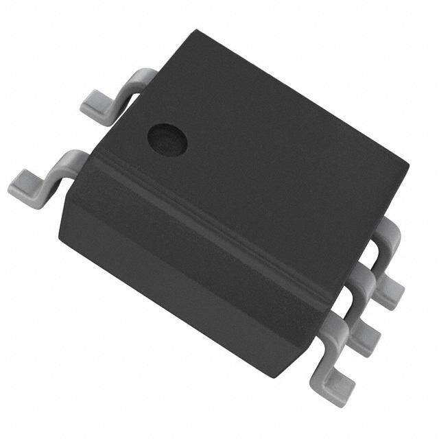
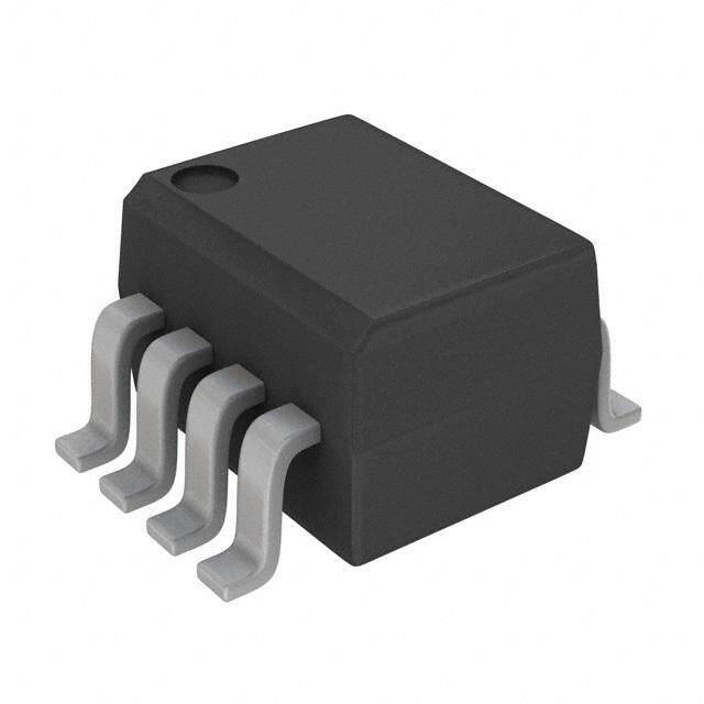
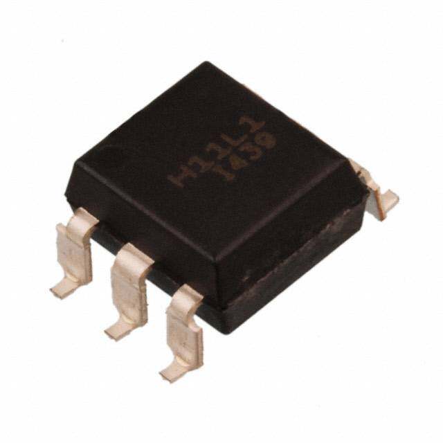
| 描述 | OPTOCOUPLER LOG-OUT 2CH 8-SMD高速光耦合器 SO-8 HS LOGIC GATE |
| 产品分类 | |
| 品牌 | Fairchild Semiconductor |
| 产品手册 | |
| 产品图片 |
|
| rohs | 符合RoHS无铅 / 符合限制有害物质指令(RoHS)规范要求 |
| 产品系列 | 光耦合器/光电耦合器,高速光耦合器,Fairchild Semiconductor HCPL2630S- |
| 数据手册 | |
| 产品型号 | HCPL2630S |
| 上升/下降时间(典型值) | 50ns, 12ns |
| 上升时间 | 50 ns |
| 下降时间 | 12 ns |
| 产品目录页面 | |
| 产品种类 | 高速光耦合器 |
| 传播延迟tpLH/tpHL(最大值) | 75ns, 75ns |
| 供应商器件封装 | 8-SMD |
| 共模瞬态抗扰度(最小值) | 10kV/µs (标准) |
| 其它名称 | HCPL-2630S |
| 包装 | 管件 |
| 单位重量 | 792 mg |
| 商标 | Fairchild Semiconductor |
| 安装类型 | 表面贴装 |
| 封装 | Bulk |
| 封装/外壳 | 8-SMD |
| 封装/箱体 | SMD-8 |
| 工作温度 | -40°C ~ 85°C |
| 工厂包装数量 | 1000 |
| 数据速率 | 10 MBd |
| 最大功率耗散 | 60 mW |
| 最大反向二极管电压 | 5 V |
| 最大工作温度 | + 85 C |
| 最大正向二极管电压 | 1.75 V |
| 最大正向二极管电流 | 30 mA |
| 最大连续输出电流 | 50 mA |
| 最小工作温度 | - 40 C |
| 标准包装 | 1,000 |
| 每芯片的通道数量 | 2 Channels |
| 电压-正向(Vf)(典型值) | 1.4V |
| 电压-电源 | 4.5 V ~ 5.5 V |
| 电压-隔离 | 2500Vrms |
| 电流-DC正向(If) | 30mA |
| 电流-输出/通道 | 50mA |
| 系列 | HCPL2630 |
| 绝缘电压 | 2500 Vrms |
| 输入-输入侧1/输入侧2 | 2/0 |
| 输入类型 | DC |
| 输出类型 | 开路集电极 |
| 输出设备 | Photo IC |
| 通道数 | 2 |
| 零件号别名 | HCPL2630S_NL |


.jpg)

- 商务部:美国ITC正式对集成电路等产品启动337调查
- 曝三星4nm工艺存在良率问题 高通将骁龙8 Gen1或转产台积电
- 太阳诱电将投资9.5亿元在常州建新厂生产MLCC 预计2023年完工
- 英特尔发布欧洲新工厂建设计划 深化IDM 2.0 战略
- 台积电先进制程称霸业界 有大客户加持明年业绩稳了
- 达到5530亿美元!SIA预计今年全球半导体销售额将创下新高
- 英特尔拟将自动驾驶子公司Mobileye上市 估值或超500亿美元
- 三星加码芯片和SET,合并消费电子和移动部门,撤换高东真等 CEO
- 三星电子宣布重大人事变动 还合并消费电子和移动部门
- 海关总署:前11个月进口集成电路产品价值2.52万亿元 增长14.8%


PDF Datasheet 数据手册内容提取
Is Now Part of To learn more about ON Semiconductor, please visit our website at www.onsemi.com Please note: As part of the Fairchild Semiconductor integration, some of the Fairchild orderable part numbers will need to change in order to meet ON Semiconductor’s system requirements. Since the ON Semiconductor product management systems do not have the ability to manage part nomenclature that utilizes an underscore (_), the underscore (_) in the Fairchild part numbers will be changed to a dash (-). This document may contain device numbers with an underscore (_). Please check the ON Semiconductor website to verify the updated device numbers. The most current and up-to-date ordering information can be found at www.onsemi.com. Please email any questions regarding the system integration to Fairchild_questions@onsemi.com. ON Semiconductor and the ON Semiconductor logo are trademarks of Semiconductor Components Industries, LLC dba ON Semiconductor or its subsidiaries in the United States and/or other countries. ON Semiconductor owns the rights to a number of patents, trademarks, copyrights, trade secrets, and other intellectual property. A listing of ON Semiconductor’s product/patent coverage may be accessed at www.onsemi.com/site/pdf/Patent-Marking.pdf. ON Semiconductor reserves the right to make changes without further notice to any products herein. ON Semiconductor makes no warranty, representation or guarantee regarding the suitability of its products for any particular purpose, nor does ON Semiconductor assume any liability arising out of the application or use of any product or circuit, and specifically disclaims any and all liability, including without limitation special, consequential or incidental damages. Buyer is responsible for its products and applications using ON Semiconductor products, including compliance with all laws, regulations and safety requirements or standards, regardless of any support or applications information provided by ON Semiconductor. “Typical” parameters which may be provided in ON Semiconductor data sheets and/or specifications can and do vary in different applications and actual performance may vary over time. All operating parameters, including “Typicals” must be validated for each customer application by customer’s technical experts. ON Semiconductor does not convey any license under its patent rights nor the rights of others. ON Semiconductor products are not designed, intended, or authorized for use as a critical component in life support systems or any FDA Class 3 medical devices or medical devices with a same or similar classification in a foreign jurisdiction or any devices intended for implantation in the human body. Should Buyer purchase or use ON Semiconductor products for any such unintended or unauthorized application, Buyer shall indemnify and hold ON Semiconductor and its officers, employees, subsidiaries, affiliates, and distributors harmless against all claims, costs, damages, and expenses, and reasonable attorney fees arising out of, directly or indirectly, any claim of personal injury or death associated with such unintended or unauthorized use, even if such claim alleges that ON Semiconductor was negligent regarding the design or manufacture of the part. ON Semiconductor is an Equal Opportunity/Affirmative Action Employer. This literature is subject to all applicable copyright laws and is not for resale in any manner.
S in g le January 2011 - C h a n n e Single-Channel: 6N137, HCPL2601, HCPL2611 l: 6 N Dual-Channel: HCPL2630, HCPL2631 1 3 7 High Speed 10MBit/s Logic Gate Optocouplers , H C P L Features Description 2 6 0 ■ Very high speed – 10 MBit/s The 6N137, HCPL2601, HCPL2611 single-channel and 1 ■ Superior CMR – 10 kV/µs HCPL2630, HCPL2631 dual-channel optocouplers , H ■ Double working voltage-480V consist of a 850 nm AlGaAS LED, optically coupled to a C P ■ Fan-out of 8 over -40°C to +85°C very high speed integrated photo-detector logic gate with L 2 ■ Logic gate output a strobable output. This output features an open collec- 6 tor, thereby permitting wired OR outputs. The coupled 1 ■ Strobable output 1 parameters are guaranteed over the temperature range D ■ Wired OR-open collector of -40°C to +85°C. A maximum input signal of 5mA will u ■ U.L. recognized (File # E90700) a provide a minimum output sink current of 13mA (fan out l- C Applications of 8). h a An internal noise shield provides superior common n ■ Ground loop elimination n mode rejection of typically 10kV/µs. The HCPL2601 and e ■ LSTTL to TTL, LSTTL or 5-volt CMOS HCPL2631 has a minimum CMR of 5kV/µs. The l: H ■ Line receiver, data transmission HCPL2611 has a minimum CMR of 10kV/µs. C P ■ Data multiplexing L ■ Switching power supplies 26 3 ■ Pulse transformer replacement 0 ■ Computer-peripheral interface , H C P L 2 Schematics Package Outlines 6 3 1 — H ig h N/C 1 8 VCC + 1 8 VCC 8 Sp 1 e V e F1 d + 2 7 VE _ 2 7 V01 10M V B F 8 it _ 3 6 VO _ 3 6 V02 1 8 /s L 1 o V g F2 ic N/C4 5 GND + 4 5 GND Truth Table (Positive Logic) G a Input Enable Output te O H H L p 6N137 HCPL2630 L H H to HCPL2601 HCPL2631 c HCPL2611 H L H o u L L H p A 0.1µF bypass capacitor must be connected between pins 8 and 5(1). H NC L ler s L NC H ©2005 Fairchild Semiconductor Corporation www.fairchildsemi.com 6N137, HCPL2601, HCPL2611, HCPL2630, HCPL2631 Rev. 1.0.8
S in Absolute Maximum Ratings (T = 25°C unless otherwise specified) g A le Stresses exceeding the absolute maximum ratings may damage the device. The device may not function or be - C operable above the recommended operating conditions and stressing the parts to these levels is not recommended. h In addition, extended exposure to stresses above the recommended operating conditions may affect device reliability. a n The absolute maximum ratings are stress ratings only. n e l: Symbol Parameter Value Units 6 N T Storage Temperature -55 to +125 °C 1 STG 3 7 TOPR Operating Temperature -40 to +85 °C , H T Lead Solder Temperature (for wave soldering only)* 260 for 10 sec °C C SOL P EMITTER L 2 6 IF DC/Average Forward Single Channel 50 mA 0 1 Input Current Dual Channel (Each Channel) 30 , H C V Enable Input Voltage Not to Exceed Single Channel 5.5 V E P V by more than 500mV L CC 2 V Reverse Input Voltage Each Channel 5.0 V 6 R 1 1 PI Power Dissipation Single Channel 100 mW D u Dual Channel (Each Channel) 45 a l- DETECTOR C h V Supply Voltage 7.0 V a CC n (1 minute max) n e I Output Current Single Channel 50 mA l: O H Dual Channel (Each Channel) 50 C P V Output Voltage Each Channel 7.0 V L O 2 6 PO Collector Output Single Channel 85 mW 3 0 Power Dissipation Dual Channel (Each Channel) 60 , H C *For peak soldering reflow, please refer to the Reflow Profile on page 11. P L 2 6 3 1 — Recommended Operating Conditions H ig The Recommended Operating Conditions table defines the conditions for actual device operation. Recommended h operating conditions are specified to ensure optimal performance to the datasheet specifications. Fairchild does not S p recommend exceeding them or designing to absolute maximum ratings. e e d Symbol Parameter Min. Max. Units 1 0 IFL Input Current, Low Level 0 250 µA M B IFH Input Current, High Level *6.3 15 mA it /s VCC Supply Voltage, Output 4.5 5.5 V L o V Enable Voltage, Low Level 0 0.8 V EL g V Enable Voltage, High Level 2.0 V V ic EH CC G T Low Level Supply Current -40 +85 °C a A t e N Fan Out (TTL load) 8 O p *6.3mA is a guard banded value which allows for at least 20% CTR degradation. Initial input current threshold value to is 5.0mA or less. c o u p le r s ©2005 Fairchild Semiconductor Corporation www.fairchildsemi.com 6N137, HCPL2601, HCPL2611, HCPL2630, HCPL2631 Rev. 1.0.8 2
S in Electrical Characteristics (T = 0 to 70°C unless otherwise specified) g A le - Individual Component Characteristics C h Symbol Parameter Test Conditions Min. Typ.* Max. Unit a n n EMITTER e l: VF Input Forward Voltage IF = 10mA 1.8 V 6 N TA = 25°C 1.4 1.75 1 3 B Input Reverse Breakdown I = 10µA 5.0 V 7 VR Voltage R , H C C Input Capacitance V = 0, f = 1MHz 60 pF P IN F L ∆V / ∆T Input Diode Temperature I = 10mA -1.4 mV/°C 2 F A F 6 Coefficient 0 1 DETECTOR , H I High Level Supply Current V = 5.5V, I = 0mA, Single Channel 7 10 mA C CCH CC F P VE = 0.5V Dual Channel 10 15 L 2 6 ICCL Low Level Supply Current Single Channel VCC = 5.5V, 9 13 mA 1 I = 10mA 1 F D Dual Channel V = 0.5V 14 21 u E a IEL Low Level Enable Current VCC = 5.5V, VE = 0.5V -0.8 -1.6 mA l-C I High Level Enable Current V = 5.5V, V = 2.0V -0.6 -1.6 mA h EH CC E a n VEH High Level Enable Voltage VCC = 5.5V, IF = 10mA 2.0 V n VEL Low Level Enable Voltage VCC = 5.5V, IF = 10mA(3) 0.8 V el: H C Switching Characteristics (T = -40°C to +85°C, V = 5V, I = 7.5mA unless otherwise specified) P A CC F L 2 Symbol AC Characteristics Test Conditions Min. Typ.* Max. Unit 6 3 T Propagation Delay R = 350Ω, T = 25°C 20 45 75 ns 0 PLH Time to Output HIGH CL = 15pF(4) (Fig. 12) A , H L 100 Level C P T Propagation Delay T = 25°C(5) 25 45 75 ns L PHL A 2 Time to Output LOW RL = 350Ω, CL = 15pF (Fig. 12) 100 63 Level 1 |T –T | Pulse Width Distortion (R = 350Ω, C = 15pF (Fig. 12) 3 35 ns — PHL PLH L L H tr Output Rise Time RL = 350Ω, CL = 15pF(6) (Fig. 12) 50 ns ig (10–90%) h t Output Rise Time R = 350Ω, C = 15pF(7) (Fig. 12) 12 ns S f L L p (90–10%) e e t Enable Propagation I = 7.5mA, V = 3.5V, R = 350Ω, C = 15pF(8) 20 ns d ELH F EH L L 1 Delay Time to Output (Fig. 13) 0 HIGH Level M B tEHL EDnealabyl eT iPmroep taog Oautiotpnu t I(FF i=g .7 1.53m) A, VEH = 3.5V, RL = 350Ω, CL = 15pF(9) 20 ns it/s L LOW Level o g |CMH| Common Mode TA = 25°C, |VCM| = 50V 6N137, HCPL2630 10,000 V/µs ic Transient Immunity (Peak), IF = 0mA, HCPL2601, HCPL2631 5000 10,000 G (at Output HIGH Level) VOH (Min.) = 2.0V, a R = 350Ω(10) (Fig. 14) te L O |VCM| = 400V HCPL2611 10,000 15,000 V/µs p t |CM | Common Mode R = 350Ω, I = 7.5mA, 6N137, HCPL2630 10,000 o L L F c Transient Immunity V (Max.) = 0.8V, o OL HCPL2601, HCPL2631 5000 10,000 (at Output LOW Level) TA = 25°C(11) (Fig. 14) up |V | = 400V HCPL2611 10,000 15,000 le CM r s ©2005 Fairchild Semiconductor Corporation www.fairchildsemi.com 6N137, HCPL2601, HCPL2611, HCPL2630, HCPL2631 Rev. 1.0.8 3
S in Electrical Characteristics (Continued) g le - Transfer Characteristics (T = -40 to +85°C unless otherwise specified) C A h Symbol DC Characteristics Test Conditions Min. Typ.* Max. Unit a n n I HIGH Level Output Current V = 5.5V, V = 5.5V, 100 µA e OH IFC =C 250µA, VEO = 2.0V(2) l: 6 N VOL LOW Level Output Current VCC = 5.5V, IF = 5mA, VE = 2.0V, .35 0.6 V 1 ICL = 13mA(2) 37 I Input Threshold Current V = 5.5V, V = 0.6V, V = 2.0V, 3 5 mA , H FT CC O E C I = 13mA OL P L 2 6 Isolation Characteristics (T = -40°C to +85°C unless otherwise specified.) 0 A 1 Symbol Characteristics Test Conditions Min. Typ.* Max. Unit , H C II-O Input-Output Insulation Relative humidity = 45%, 1.0* µA P Leakage Current T = 25°C, t = 5s, L A 2 V = 3000 VDC(12) 6 I-O 1 1 VISO Withstand Insulation Test RH < 50%, TA = 25°C, 2500 VRMS D Voltage II-O ≤ 2µA, t = 1 min.(12) u a RI-O Resistance (Input to Output) VI-O = 500V(12) 1012 Ω l-C C Capacitance (Input to Output) f = 1MHz(12) 0.6 pF h I-O a n n *All Typicals at V = 5V, T = 25°C CC A e l: H Notes: C 1. The V supply to each optoisolator must be bypassed by a 0.1µF capacitor or larger. This can be either a ceramic P CC or solid tantalum capacitor with good high frequency characteristic and should be connected as close as possible L 2 to the package V and GND pins of each device. 6 CC 3 0 2. Each channel. , H 3. Enable Input – No pull up resistor required as the device has an internal pull up resistor. C P 4. t – Propagation delay is measured from the 3.75mA level on the HIGH to LOW transition of the input current L PLH 2 pulse to the 1.5 V level on the LOW to HIGH transition of the output voltage pulse. 6 3 5. t – Propagation delay is measured from the 3.75mA level on the LOW to HIGH transition of the input current 1 pPuHlsLe to the 1.5 V level on the HIGH to LOW transition of the output voltage pulse. — 6. t – Rise time is measured from the 90% to the 10% levels on the LOW to HIGH transition of the output pulse. H r ig 7. t – Fall time is measured from the 10% to the 90% levels on the HIGH to LOW transition of the output pulse. h f S 8. t – Enable input propagation delay is measured from the 1.5V level on the HIGH to LOW transition of the input p ELH e voltage pulse to the 1.5V level on the LOW to HIGH transition of the output voltage pulse. e d 9. tEHL – Enable input propagation delay is measured from the 1.5V level on the LOW to HIGH transition of the input 1 voltage pulse to the 1.5V level on the HIGH to LOW transition of the output voltage pulse. 0 M 10. CM – The maximum tolerable rate of rise of the common mode voltage to ensure the output will remain in the B HIGHH state (i.e., VOUT > 2.0V). Measured in volts per microsecond (V/µs). it/s 11.CM – The maximum tolerable rate of rise of the common mode voltage to ensure the output will remain in the L L o LOW output state (i.e., V < 0.8V). Measured in volts per microsecond (V/µs). g OUT ic 12.Device considered a two-terminal device: Pins 1, 2, 3 and 4 shorted together, and Pins 5, 6, 7 and 8 shorted G together. a t e O p t o c o u p le r s ©2005 Fairchild Semiconductor Corporation www.fairchildsemi.com 6N137, HCPL2601, HCPL2611, HCPL2630, HCPL2631 Rev. 1.0.8 4
S in Typical Performance Curves g le - C Fig.1 Low Level Output Voltage vs. Ambient Temperature Fig. 2 Input Diode Forward Voltage h vs. Forward Current a 0.8 n )V( EGATLOV TUPTUO LEV 00000.....34567 CIVVF ECo= Cn= 5=d 2 itm5 iVo.A5nVs: IOL = 12.8 mA IOL = 16mA )Am( TNERRUC DRA 0113.06011 nel: 6N137, HCP EL WOL – VLO 00..12 IOL = 6.4mAIOL = 9.6mA WROF – IF0.00.0011 L2601, H 0.0 C -40 -20 0 20 40 60 80 0.9 1.0 1.1 1.2 1.3 1.4 1.5 1.6 P TA – AMBIENT TEMPERATURE (°C) VF – FORWARD VOLTAGE (V) L2 6 1 1 Fig.3 Switching Time vs. Forward Current Fig. 4 Low Level Output Current D vs. Ambient Temperature u 120 50 a )sn( Y 100 VCC = 5 V )Am( TN 45 IF = 15mA l-Cha AL RL = 4 kΩ (TPLH) ER IF = 10mA n ED NOIT 80 RUC TU 40 IF = 5mA nel: H AG 60 PT 35 C AP RL = 1 kΩ (TPLH) UO P O L L RP – TP 24000 RL = 350 Ω (TPLH) RRRLLL === 143 5kk0ΩΩ kΩ(T PHL) EVEL WOL – ILO 223050 CVVVCEOo CLn= ==d 2 it05 Vio. V6n Vs: 2630, HCP 5 7 9 11 13 15 -40 -20 0 20 40 60 80 L IF – FORWARD CURRENT (mA) TA – AMBIENT TEMPERATURE (°C) 26 3 1 Fig. 5 Input Threshold Current Fig. 6 Output Voltage vs. Input Forward Current — )Am 4 vs. Ambient Temperature 6 Hig ( TNERRU CVVCOo Cn= =d 0 it5.i6o.0 nV sV: )V( EG 5 RL = 350Ω h Spe C DLOH 3 RL = 350Ω ATLOV 4 RL = 4kΩ RL = 1kΩ ed 1 S T 3 0 E U M RH RL = 1kΩ PT B T U TUPNI – ITF 2 RL = 4kΩ O – VO 12 it/s Log ic 1-40 -20 0 20 40 60 80 00 1 2 3 4 5 6 G a TA – AMBIENT TEMPERATURE (°C) IF - FORWARD CURRENT (mA) te O p t o c o u p le r s ©2005 Fairchild Semiconductor Corporation www.fairchildsemi.com 6N137, HCPL2601, HCPL2611, HCPL2630, HCPL2631 Rev. 1.0.8 5
S Typical Performance Curves (Continued) ing le - Fig. 7 Pulse Width Distortion vs. Temperature Fig. 8 Rise and Fall Time vs. Temperature C 80 600 h a )sn( N RL = 4 kΩ )s 500 RL = 4 kΩ(tr) nne OITROTSID 4600 CIVFCo =Cn d7=i.t 5i5omAnA s: n( EMIT LLA 340000 VCIFCo =Cn d7=i.t 5i5o mnVsA: l: 6N13 HTD F DN 7, H IW ESLUP – DWP 200 RL = 1 kΩRL = 350Ω A ESIR – fT/rT 1200000 RLR =L =3 510 kΩΩ ((ttrr)) RRRLLL === 143 5kk0ΩΩΩ (tf) CPL2601, H -60 -40 -20 0 20 40 60 80 100 -60 -40 -20 0 20 40 60 80 100 C P TA – TEMPERATURE (°C) TA – TEMPERATURE (°C) L 2 6 1 1 Fig. 9 Enable Propagation Delay vs. Temperature Fig. 10 Switching Time vs. Temperature D u 120 120 a )sn( YA 100 )s RL = 4 kΩ TPLH l-Ch LED NO 80 RL = 4 kΩ (TELH) n( YALE 100 anne ITAG D NO 80 l: H APO 60 ITAG CP RP ELBANE – TE 24000 RLR =L =3 510 kΩΩ (T(TEELLHH)) RRRLLL === 3145 kk0ΩΩΩ (TEHL) APORP – TP 246000 RRLL == 13 5k0ΩΩ TTPPLLHH RRRLLL === 143 5kk0ΩΩΩ TPHL L2630, HCP -60 -40 -20 0 20 40 60 80 100 -60 -40 -20 0 20 40 60 80 100 L 2 TA – TEMPERATURE (°C) TA – TEMPERATURE (°C) 6 3 1 — Fig. 11 High Level Output Current vs. Temperature H 20 ig )A h µ( TN VCCoCn d=it i5o.n5s V: Sp ERRU 15 VIVFOE = == 2 255..005 µVVA eed C T 1 U 0 PTUO 10 MB LEV it/s EL L H 5 o GIH – gic HO G I 0 a -60 -40 -20 0 20 40 60 80 100 t e TA – TEMPERATURE (°C) O p t o c o u p le r s ©2005 Fairchild Semiconductor Corporation www.fairchildsemi.com 6N137, HCPL2601, HCPL2611, HCPL2630, HCPL2631 Rev. 1.0.8 6
S in Test Circuits g le - C Pulse h a Generator n tr = 5ns n Z O = 50Ω +5V e l: 6 N I = 7.5 mA F 1 3 1 VCC 8 I(nIF p)ut I F = 3.75 mA 7, H t t C PHL PLH P 2 7 .1 µf R Output L bypass L (VO ) 2 1.5 V 6 0 Input 3 6 Output 1 Monitor (VO ) Output 90% , H (I F ) CL (V ) C O 10% P 47 4 GND 5 L t t 2 f r 6 1 1 D u a Fig. 12 Test Circuit and Waveforms for t , t t and t l-C PLH PHL, r f h a n n e PGuelnseerator Input l: H tr = 5ns Monitor C Z O = 50Ω (V E ) PL +5V 2 6 3 0 3.0 V , H V Input C 1 CC 8 (VE ) 1.5 V P L t t 2 7.5 mA EHL ELH 6 Output 3 2 7 b.1y µpfa ss RL (VO ) 1.5 V 1 — Output H 3 6 (VO ) ig CL h S 4 5 p GND e e d 1 0 M Fig. 13 Test Circuit t and t B EHL ELH it /s L o g ic G a t e O p t o c o u p le r s ©2005 Fairchild Semiconductor Corporation www.fairchildsemi.com 6N137, HCPL2601, HCPL2611, HCPL2630, HCPL2631 Rev. 1.0.8 7
S in Test Circuits (Continued) g le - C h V a CC n 1 8 +5V n e l: 6 I N A F 2 7 .1 µf 350Ω 1 bypass 3 7 B Output , H VFF 3 6 (V ) C O P L 2 6 4 5 0 1 GND , H C P VCM L 2 6 Pulse Gen 1 1 D u a Peak l-C h a n VCM n 0V e l: H C P 5V CMH L Switching Pos. (A), I = 0 2 F 6 VO 3 0 VO (Min) , H C P V (Max) L O 2 6 3 Switching Pos. (B), I F = 7.5 mA 1 VO — 0.5 V CML H ig h S p e Fig. 14 Test Circuit Common Mode Transient Immunity e d 1 0 M B it /s L o g ic G a t e O p t o c o u p le r s ©2005 Fairchild Semiconductor Corporation www.fairchildsemi.com 6N137, HCPL2601, HCPL2611, HCPL2630, HCPL2631 Rev. 1.0.8 8
S in Ordering Information g le - Option Example Part Number Description C h S 6N137S Surface Mount Lead Bend a n n SD 6N137SD Surface Mount; Tape and Reel e l: W 6N137W 0.4" Lead Spacing 6 N V 6N137V VDE0884 1 3 7 WV 6N137WV VDE0884; 0.4” Lead Spacing , H SV 6N137SV VDE0884; Surface Mount C P SDV 6N137SDV VDE0884; Surface Mount; Tape and Reel L 2 6 0 1 , H C Marking Information P L 2 6 1 1 1 D u a 2601 2 l- C h a V XX YY T1 6 n n e l: H C 3 4 5 P L 2 6 3 0 Definitions , H C P 1 Fairchild logo L 2 2 Device number 6 3 3 VDE mark (Note: Only appears on parts ordered with VDE option – 1 See order entry table) — 4 Two digit year code, e.g., ‘03’ H ig 5 Two digit work week ranging from ‘01’ to ‘53’ h S 6 Assembly package code p e e d 1 0 M B it /s L o g ic G a t e O p t o c o u p le r s ©2005 Fairchild Semiconductor Corporation www.fairchildsemi.com 6N137, HCPL2601, HCPL2611, HCPL2630, HCPL2631 Rev. 1.0.8 9
S in Tape Specifications g le - C 12.0 ± 0.1 h 4.90 ± 0.20 an 4.0 ± 0.1 Ø1.55 ± 0.05 ne 0.30 ± 0.05 4.0 ± 0.1 1.75 ± 0.10 l: 6 N 1 3 7 , H 7.5 ± 0.1 C 13.2 ± 0.2 16.0 ± 0.3 PL 10.30 ± 0.20 2 6 0 1 , H C 0.1 MAX 10.30 ± 0.20 Ø1.6 ± 0.1 P L 2 User Direction of Feed 61 1 D u a l- C h Reflow Profile a n n e 300 l: 215 C, 10–30 s H 250 C e (°C) 200 225 C peak PL2 ur 6 at 150 3 mper 100 Time above 183C, 60–150 sec 0, H e C T 50 Ramp up = 3C/sec P L 0 2 0 0.5 1 1.5 2 2.5 3 3.5 4 4.5 6 3 Time (Minute) 1 — •• PTiemaek oref ftleomw pteemraptuerrea thuirgeh: e2r2 t5hCan ( p1a8c3kCa gfoer s6u0r–fa1c5e0 tseemcpoenrdasture) H • One time soldering reflow is recommended ig h S p e e d 1 0 M B it /s L o g ic G a t e O p t o c o u p le r s ©2005 Fairchild Semiconductor Corporation www.fairchildsemi.com 6N137, HCPL2601, HCPL2611, HCPL2630, HCPL2631 Rev. 1.0.8 10
None
None
None
ON Semiconductor and are trademarks of Semiconductor Components Industries, LLC dba ON Semiconductor or its subsidiaries in the United States and/or other countries. ON Semiconductor owns the rights to a number of patents, trademarks, copyrights, trade secrets, and other intellectual property. A listing of ON Semiconductor’s product/patent coverage may be accessed at www.onsemi.com/site/pdf/Patent−Marking.pdf. ON Semiconductor reserves the right to make changes without further notice to any products herein. ON Semiconductor makes no warranty, representation or guarantee regarding the suitability of its products for any particular purpose, nor does ON Semiconductor assume any liability arising out of the application or use of any product or circuit, and specifically disclaims any and all liability, including without limitation special, consequential or incidental damages. Buyer is responsible for its products and applications using ON Semiconductor products, including compliance with all laws, regulations and safety requirements or standards, regardless of any support or applications information provided by ON Semiconductor. “Typical” parameters which may be provided in ON Semiconductor data sheets and/or specifications can and do vary in different applications and actual performance may vary over time. All operating parameters, including “Typicals” must be validated for each customer application by customer’s technical experts. ON Semiconductor does not convey any license under its patent rights nor the rights of others. ON Semiconductor products are not designed, intended, or authorized for use as a critical component in life support systems or any FDA Class 3 medical devices or medical devices with a same or similar classification in a foreign jurisdiction or any devices intended for implantation in the human body. Should Buyer purchase or use ON Semiconductor products for any such unintended or unauthorized application, Buyer shall indemnify and hold ON Semiconductor and its officers, employees, subsidiaries, affiliates, and distributors harmless against all claims, costs, damages, and expenses, and reasonable attorney fees arising out of, directly or indirectly, any claim of personal injury or death associated with such unintended or unauthorized use, even if such claim alleges that ON Semiconductor was negligent regarding the design or manufacture of the part. ON Semiconductor is an Equal Opportunity/Affirmative Action Employer. This literature is subject to all applicable copyright laws and is not for resale in any manner. PUBLICATION ORDERING INFORMATION LITERATURE FULFILLMENT: N. American Technical Support: 800−282−9855 Toll Free ON Semiconductor Website: www.onsemi.com Literature Distribution Center for ON Semiconductor USA/Canada 19521 E. 32nd Pkwy, Aurora, Colorado 80011 USA Europe, Middle East and Africa Technical Support: Order Literature: http://www.onsemi.com/orderlit Phone: 303−675−2175 or 800−344−3860 Toll Free USA/Canada Phone: 421 33 790 2910 Fax: 303−675−2176 or 800−344−3867 Toll Free USA/Canada Japan Customer Focus Center For additional information, please contact your local Email: orderlit@onsemi.com Phone: 81−3−5817−1050 Sales Representative © Semiconductor Components Industries, LLC www.onsemi.com www.onsemi.com 1
Mouser Electronics Authorized Distributor Click to View Pricing, Inventory, Delivery & Lifecycle Information: O N Semiconductor: HCPL2630SD HCPL2630S HCPL2630SV HCPL2630 HCPL2630WV HCPL2630SDV HCPL2630V