ICGOO在线商城 > 隔离器 > 光隔离器 - 晶体管,光电输出 > HCPL-0500
 Datasheet下载
- 型号: HCPL-0500
- 制造商: Avago Technologies
- 库位|库存: xxxx|xxxx
- 要求:
| 数量阶梯 | 香港交货 | 国内含税 |
| +xxxx | $xxxx | ¥xxxx |
查看当月历史价格
查看今年历史价格
HCPL-0500产品简介:
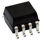
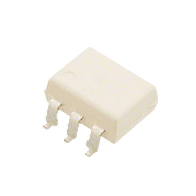
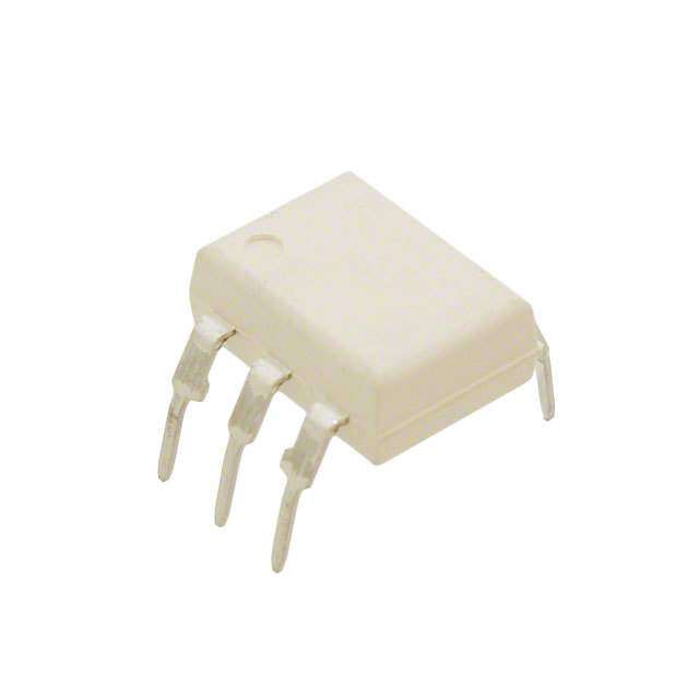
ICGOO电子元器件商城为您提供HCPL-0500由Avago Technologies设计生产,在icgoo商城现货销售,并且可以通过原厂、代理商等渠道进行代购。 HCPL-0500价格参考。Avago TechnologiesHCPL-0500封装/规格:光隔离器 - 晶体管,光电输出, 光隔离器 有基极的晶体管 输出 3750Vrms 1 通道 8-SO。您可以下载HCPL-0500参考资料、Datasheet数据手册功能说明书,资料中有HCPL-0500 详细功能的应用电路图电压和使用方法及教程。
Broadcom Limited的HCPL-0500是一款光隔离器,具体分类为晶体管光电输出型。该器件通过光耦合技术实现电信号的隔离传输,广泛应用于需要电气隔离和信号传递的场景中。以下是HCPL-0500的主要应用场景:

1. 工业自动化:在工业控制系统中,如可编程逻辑控制器(PLC)、分布式控制系统(DCS)等,HCPL-0500用于隔离输入输出信号,防止电磁干扰(EMI)和地环路问题,确保系统的稳定性和可靠性。

2. 电力系统:在电力监控、保护装置和智能电表中,HCPL-0500可以隔离高压侧与低压侧的信号,保护低电压电路免受高电压冲击,提高系统的安全性。

3. 通信设备:在通信基站、路由器、交换机等设备中,HCPL-0500用于隔离不同模块之间的信号,避免电源噪声和信号干扰,保证数据传输的准确性和稳定性。

4. 医疗设备:在医疗仪器如心电图机、监护仪等中,HCPL-0500用于隔离患者与设备之间的电气连接,确保患者安全,同时防止外部干扰影响测量精度。

5. 汽车电子:在汽车的传感器、控制器和执行器之间,HCPL-0500用于信号隔离,防止车载电子系统中的电磁干扰,确保车辆的安全和可靠运行。

6. 消费电子:在一些高端消费电子产品中,如音响设备、智能家居控制器等,HCPL-0500用于隔离不同部分的电路,提升产品的抗干扰能力和使用寿命。

总之,HCPL-0500凭借其可靠的电气隔离性能和稳定的信号传输能力,在各种需要电气隔离和信号传递的应用中发挥着重要作用,适用于对可靠性要求较高的场合。
| 参数 | 数值 |
| 产品目录 | |
| 描述 | OPTOISO 3.75KV TRANS W/BASE 8SO |
| 产品分类 | |
| 品牌 | Avago Technologies US Inc. |
| 数据手册 | http://www.avagotech.com/docs/AV02-0171EN |
| 产品图片 |
|
| 产品型号 | HCPL-0500 |
| PCN封装 | |
| rohs | 含铅 / 不符合限制有害物质指令(RoHS)规范要求 |
| 产品系列 | - |
| Vce饱和值(最大值) | - |
| 上升/下降时间(典型值) | - |
| 产品目录绘图 |
|
| 供应商器件封装 | 8-SO |
| 其它名称 | 516-1024-5 |
| 包装 | 管件 |
| 安装类型 | 表面贴装 |
| 封装/外壳 | 8-SOIC(0.154",3.90mm 宽) |
| 工作温度 | -55°C ~ 100°C |
| 打开/关闭时间(典型值) | 0.2µs, 1.3µs |
| 标准包装 | 100 |
| 电压-正向(Vf)(典型值) | 1.5V |
| 电压-输出(最大值) | 20V |
| 电压-隔离 | 3750Vrms |
| 电流-DC正向(If) | 25mA |
| 电流-输出/通道 | 8mA |
| 电流传输比(最大值) | - |
| 电流传输比(最小值) | 5% @ 16mA |
| 输入类型 | DC |
| 输出类型 | 有基极的晶体管 |
| 通道数 | 1 |


(B)(TU)-VG.jpg)


- 商务部:美国ITC正式对集成电路等产品启动337调查
- 曝三星4nm工艺存在良率问题 高通将骁龙8 Gen1或转产台积电
- 太阳诱电将投资9.5亿元在常州建新厂生产MLCC 预计2023年完工
- 英特尔发布欧洲新工厂建设计划 深化IDM 2.0 战略
- 台积电先进制程称霸业界 有大客户加持明年业绩稳了
- 达到5530亿美元!SIA预计今年全球半导体销售额将创下新高
- 英特尔拟将自动驾驶子公司Mobileye上市 估值或超500亿美元
- 三星加码芯片和SET,合并消费电子和移动部门,撤换高东真等 CEO
- 三星电子宣布重大人事变动 还合并消费电子和移动部门
- 海关总署:前11个月进口集成电路产品价值2.52万亿元 增长14.8%


.jpg)
PDF Datasheet 数据手册内容提取
6N135/6, HCNW135/6, HCPL-2502/0500/0501 Single-Channel, High-Speed Optocouplers Data Sheet Description Features These diode-transistor optocouplers use an insulating layer High speed: 1 Mb/s between a LED and an integrated photodetector to provide TTL compatible electrical insulation between input and output. Separate Available in 8-pin DIP, SO-8, widebody packages connections for the photodiode bias and output-transistor Open collector output collector increase the speed up to a hundred times that of a conventional phototransistor coupler by reducing the Safety approval base-collector capacitance. UL Recognized – 3750 V for 1 minute (5000 V for rms rms 1minute for HCNW and Option 020 devices) per UL1577 These single channel optocouplers are available in 8-pin DIP, CSA Approved SO-8, and Widebody package configurations. IEC/EN/DIN EN 60747-5-5 Approved The 6N135, HCPL-0500, and HCNW135 are for use in — V = 567V peak for SO-8 devices TTL/CMOS, TTL/LSTTL or wide-bandwidth analog applications. IORM Current transfer ratio (CTR) for these devices is 7% minimum at — VIORM = 630V peak for DIP 300 mil devices I = 16 mA. — V = 1414V peak for DIP 400 mil (widebody) F IORM devices The 6N136, HCPL-2502, HCPL-0501, and HCNW136 are designed for high-speed TTL/TTL applications. A standard Dual channel version available (253X/053X/0534) 16-mA TTL sink current through the input LED will provide enough output current for 1 TTL load and a 5.6 k pull-up Applications resistor. CTR for these devices is 19% minimum at I =16 mA. F High voltage insulation Video signal isolation Line receivers Feedback element in switched mode power supplies High speed logic ground isolation — TTL/TTL, TTL/CMOS, TTL/LSTTL Replaces pulse transformers Replaces slow phototransistor isolators Analog signal ground isolation CAUTION It is advised that normal static precautions be taken in handling and assembly of this component to prevent damage and/or degradation which may be induced by ESD. Broadcom - 1 -
6N135/6, HCNW135/6, HCPL-2502/0500/0501 Data Sheet Functional Diagram Schematic I CC 8 NC 1 8 VCC VCC TRUTH TABLE (POSITIVE LOGIC) ANODE 2 7 VB LED VO 2 IF ANODE ON LOW + CATHODE 3 6 VO OFF HIGH V F IO 6 NC 4 5 GND - VO CATHODE 3 5 Truth Table (Positive Logic) SHIELD GND LED V0 IB 7 ON LOW VB OFF HIGH A 0.1-μF bypass capacitor must be connected between pins 5 and 8. Selection Guide Widebody Minimum CMR 8-Pin DIP (300 Mil) Small Outline SO-8 (400Mil) Current Transfer Single Channel Dual Channel Single Channel Dual Channel Single Channel dV/dT (V/μs) VCM (V) Ratio (%) Package Packagea Package Packagea Package 1000 10 7 6N135 HCPL-2530 HCPL-0500 HCPL-0530 HCNW135 19 6N136 HCPL-2531 HCPL-0501 HCPL-0531 HCNE136 15 HCPL-2502 a. Technical data for these products are on separate Broadcom publications. Broadcom - 2 -
6N135/6, HCNW135/6, HCPL-2502/0500/0501 Data Sheet Ordering Information 6N135, 6N136, HCPL-2502, HCPL-0500, HCPL-0501 are UL Recognized with 3750 V for 1 minute per UL1577. rms HCNW135 and HCNW136 are UL Recognized with 5000 V for 1 minute per UL1577. All these devices are approved under CSA rms Component Acceptance Notice #5, File CA 88324. Option UL 5000 IEC/EN/DIN Part Package Surface Gull Wing Tape and Vrms/ EN Quantity Number RoHS Non RoHS Mount Reel 1Minute 60747-5-5 Compliant Compliant Rating 6N135 -000E No option 300mil DIP-8 50 per tube 6N136 -300E #300 X X 50 per tube HCPL-2502 -500E #500 X X X 1000 per reel -020E #020 X 50 per tube -320E #320 X X X 50 per tube -520E #520 X X X X 1000 per reel -060E #060 X 50 per tube -360E #360 X X X 50 per tube -560E #560 X X X X 1000 per reel HCPL-0500 -000E No option SO-8 100 per tube HCPL-0501 -500E #500 X X X 1500 per reel -060E #060 X 100 per tube -560E #560 X X X X 1500 per reel HCNW135 -000E No option 400 mil X X 42 per tube Widebody HCNW136 -300E #300 X X X X 42 per tube DIP-8 -500E #500 X X X X X 750 per reel To order, choose a part number from the part number column and combine with the desired option from the option column to form an order entry. Example 1: HCPL-2502-560E to order product of 300 mil DIP Gull Wing Surface Mount package in Tape and Reel packaging with IEC/EN/DIN EN 60747-5-5 Safety Approval in RoHS compliant. Example 2: HCPL-2502 to order product of 300 mil DIP package in tube packaging and non RoHS compliant. Option data sheets are available. Contact your Broadcom sales representative or authorized distributor for information. NOTE The notation ‘#XXX’ is used for existing products, while (new) products launched since 15th July 2001 and RoHS compliant option will use ‘-XXXE‘. Broadcom - 3 -
6N135/6, HCNW135/6, HCPL-2502/0500/0501 Data Sheet Package Outline Drawings 8-Pin DIP Package (6N135/6, HCPL-2502) 9.65 ± 0.25 7.62 ± 0.25 (0.380 ± 0.010) (0.300 ± 0.010) TYPE NUMBER 8 7 6 5 6.35 ± 0.25 OPTION CODE* (0.250 ± 0.010) A XXXXZ DATE CODE YYWW RU EEE UL RECOGNITION LOT ID 1 2 3 4 1.78 (0.070) MAX. 1.19 (0.047) MAX. + 0.076 5(cid:113) TYP. 0.254 - 0.051 + 0.003) 3.56 ± 0.13 4.70 (0.185) MAX. (0.010 - 0.002) (0.140 ± 0.005) 0.51 (0.020) MIN. 2.92 (0.115) MIN. DIMENSIONS IN MILLIMETERS AND (INCHES). *MARKING CODE LETTER FOR OPTION NUMBERS "L" = OPTION 020 1.080 ± 0.320 0.65 (0.025) MAX. "V" = OPTION 060 (0.043 ± 0.013) OPTION NUMBERS 300 AND 500 NOT MARKED. 2.54 ± 0.25 (0.100 ± 0.010) NOTE: FLOATING LEAD PROTRUSION IS 0.25 mm (10 mils) MAX. Broadcom - 4 -
6N135/6, HCNW135/6, HCPL-2502/0500/0501 Data Sheet 8-Pin DIP Package with Gull Wing Surface Mount Option 300 (6N135/6) LAND PATTERN RECOMMENDATION 9.65 ± 0.25 1.016 (0.040) (0.380 ± 0.010) 8 7 6 5 6.350 ± 0.25 10.9 (0.430) (0.250 ± 0.010) 1 2 3 4 2.0 (0.080) 1.27 (0.050) 1.780 9.65 ± 0.25 (0.070) (0.380 ± 0.010) 1.19 MAX. (0.047) 7.62 ± 0.25 MAX. (0.300 ± 0.010) + 0.076 0.254 - 0.051 3.56 ± 0.13 + 0.003) (0.140 ± 0.005) (0.010 - 0.002) 1.080 ± 0.320 0.635 ± 0.25 (0.043 ± 0.013) (0.025 ± 0.010) 12(cid:113) NOM. 2.54 0.635 ± 0.130 (0.100) (0.025 ± 0.005) BSC DIMENSIONS IN MILLIMETERS (INCHES). LEAD COPLANARITY = 0.10 mm (0.004 INCHES). NOTE: FLOATING LEAD PROTRUSION IS 0.25 mm (10 mils) MAX. Broadcom - 5 -
6N135/6, HCNW135/6, HCPL-2502/0500/0501 Data Sheet Small Outline SO-8 Package (HCPL-0500/1) LAND PATTERN RECOMMENDATION 8 7 6 5 5.994 ± 0.203 (0.236 ± 0.008) XXX 3.937 ± 0.127 YWW TYPE NUMBER 7.49 (0.295) (0.155 ± 0.005) (LAST 3 DIGITS) EEE DATE CODE LOT ID PIN ONE 1 2 3 4 1.9 (0.075) 0.406 ± 0.076 (0.016 ± 0.003) 1.270 BSC 0.64 (0.025) (0.050) * 5.080 ± 0.127 7(cid:113) 0.432 45(cid:113) X (0.200 ± 0.005) (0.017) 3.175 ± 0.127 (0.125 ± 0.005) 0 ~ 7(cid:113) 0.228 ± 0.025 1.524 (0.009 ± 0.001) (0.060) 0.203 ± 0.102 *TOTAL PACKAGE LENGTH (INCLUSIVE OF MOLD FLASH) (0.008 ± 0.004) 5.207 ± 0.254 (0.205 ± 0.010) 0.305 MIN. (0.012) DIMENSIONS IN MILLIMETERS (INCHES). LEAD COPLANARITY = 0.10 mm (0.004 INCHES) MAX. Broadcom - 6 -
6N135/6, HCNW135/6, HCPL-2502/0500/0501 Data Sheet 8-Pin Widebody DIP Package (HCNW135/6) 11.23 ± 0.15 11.00 MAX. (0.442 ± 0.006) (0.433) 9.00 ± 0.15 8 7 6 5 (0.354 ± 0.006) TYPE NUMBER A DATE CODE HCNWXXXX YYWW EEE LOT ID 1 2 3 4 10.16 (0.400) TYP. 1.55 (0.061) MAX. 7(cid:113) TYP. 0.254 + 0.076 - 0.0051 + 0.003) (0.010 - 0.002) 5.10 MAX. (0.201) 3.10 (0.122) 3.90 (0.154) 0.51 (0.021) MIN. 2.54 (0.100) TYP. DIMENSIONS IN MILLIMETERS (INCHES). 1.8 ± 0.15 0.40 (0.016) (0.071 ± 0.006) 0.56 (0.022) NOTE: FLOATING LEAD PROTRUSION IS 0.25 mm (10 mils) MAX. Broadcom - 7 -
6N135/6, HCNW135/6, HCPL-2502/0500/0501 Data Sheet 8-Pin Widebody DIP Package with Gull Wing Surface Mount Option 300 (HCNW135/6) 11.23 ± 0.15 (0.442 ± 0.006) LAND PATTERN RECOMMENDATION 8 7 6 5 9.00 ± 0.15 (0.354 ± 0.006) 13.56 (0.534) 1 2 3 4 1.3 2.29 (0.051) (0.09) 1.55 12.30 ± 0.30 (0.061) (0.484 ± 0.012) MAX. 11.00 MAX. (0.433) + 0.076 0.254 - 0.0051 4.00 MAX. (0.010+ 0.003) (0.158) - 0.002) 1.80 ± 0.15 (0.071 ± 0.006) 1.00 ± 0.15 0.75 ± 0.25 (0.039 ± 0.006) 2.54 (0.030 ± 0.010) (0.100) BSC 7(cid:113) NOM. DIMENSIONS IN MILLIMETERS (INCHES). LEAD COPLANARITY = 0.10 mm (0.004 INCHES). NOTE: FLOATING LEAD PROTRUSION IS 0.25 mm (10 mils) MAX. Solder Reflow Profile Recommended reflow conditions are as per JEDEC Standard, J-STD-020 (latest revision). Non-halide flux should be used. Regulatory Information The devices contained in this data sheet have been approved by the following organizations: UL Approval under UL 1577, Component Recognition Program, File E55361. CSA Approval under CSA Component Acceptance Notice #5, File CA 88324. IEC/EN/DIN EN 60747-5-5 (HCNW and Option 060/360/560 only) Broadcom - 8 -
6N135/6, HCNW135/6, HCPL-2502/0500/0501 Data Sheet Insulation and Safety Related Specifications 8-Pin DIP Widebody Parameter Symbol (300Mil) SO-8 Value (400 Mill) Units Conditions Value Value Minimum External Air Gap L(101) 7.1 4.9 9.6 mm Measured from input terminals to output (External Clearance) terminals, shortest distance through air. Minimum External Tracking L(102) 7.4 4.8 10.0 mm Measured from input terminals to output (External Creepage) terminals, shortest distance path along body.. Minimum Internal Plastic Gap 0.08 0.08 1.0 mm Through insulation distance conductor to (Internal Clearance) conductor, usually the direct distance between the photoemitter and photodetector inside the optocoupler cavity. Minimum Internal Tracking N/A N/A 4.0 mm Measured from input terminals to output (Internal Creepage) terminals, along internal cavity. Tracking Resistance CTI 200 200 200 V DIN IEC 112/VDE 0303 Part 1 (Comparative Tracking Index) Isolation Group IIIa IIIa IIIa Material Group (DIN VDE 0110, 1/89, Table 1) Option 300 – Surface mount classification is Class A in accordance with CECC 00802. Broadcom - 9 -
6N135/6, HCNW135/6, HCPL-2502/0500/0501 Data Sheet a IEC/EN/DIN EN 60747-5-5 Insulation Characteristics (Option 060 Only) Description Symbol 8-Pin DIP SO-8 Units Installation Classification per DIN VDE 0110/39, Table 1 for rated mains voltage 150 V I – IV I – IV rms for rated mains voltage 300 V I – IV I – IV rms I – IV I – III for rated mains voltage 600 V rms Climatic Classification 0/70/21 0/70/21 Pollution Degree (DIN VDE 0110/39) 2 2 Maximum Working Insulation Voltage V 630 567 V IORM peak Input to Output Test Voltage, Method ba VPR 1181 1063 Vpeak V × 1.875 = V , 100% Production Test with t = 1s, Partial Discharge < 5 pC IORM PR m Input to Output Test Voltage, Method aa VPR 1008 907 Vpeak V x 1.6 = V , Type and Sample Test, t = 10s, Partial Discharge < 5 pC IORM PR m Highest Allowable Overvoltagea (Transient Overvoltage tini = 60s) VIOTM 8000 6000 Vpeak Safety-limiting values – Maximum Values Allowed in the Event of a Failure Case Temperature T 175 150 °C S Input Current IS, INPUT 230 150 mA Output Power PS, OUTPUT 600 600 mW Insulation Resistance at TS, VIO = 500V RS ≥109 ≥109 a. Refer to the front of the optocoupler section of the current catalog, under Product Safety Regulations section IEC/EN/DIN EN 60747-5-5, for a detailed description. NOTE Isolation characteristics are guaranteed only within the safety maximum ratings, which must be ensured by protective circuits in the application. Broadcom - 10 -
6N135/6, HCNW135/6, HCPL-2502/0500/0501 Data Sheet a IEC/EN/DIN EN 60747-5-5 Insulation Characteristics (HCNW135/6 Option 060 Only) Description Symbol Characteristic Units Installation Classification per DIN VDE 0110/39, Table 1 for rated mains voltage 150 V I – IV rms for rated mains voltage 300 V I – IV rms I – IV for rated mains voltage 600 V rms I – III for rated mains voltage 1000 V rms Climatic Classification 0/70/21 Pollution Degree (DIN VDE 0110/39) 2 Maximum Working Insulation Voltage V 1414 V IORM peak Input to Output Test Voltage, Method ba VPR 2651 Vpeak V × 1.875 = V , 100% Production Test with t = 1s, Partial Discharge < 5 pC IORM PR m Input to Output Test Voltage, Method aa VPR 2262 Vpeak V x 1.6 = V , Type and Sample Test, t = 10s, Partial Discharge < 5 pC IORM PR m Highest Allowable Overvoltagea (Transient Overvoltage tini = 60s) VIOTM 8000 Vpeak Safety-limiting values – Maximum Values Allowed in the Event of a Failure Case Temperature T 150 °C S Input Current IS, INPUT 400 mA Output Power PS, OUTPUT 700 mW Insulation Resistance at TS, VIO = 500V RS ≥109 a. Refer to the front of the optocoupler section of the current catalog, under Product Safety Regulations section IEC/EN/DIN EN 60747-5-5, for a detailed description. NOTE Isolation characteristics are guaranteed only within the safety maximum ratings, which must be ensured by protective circuits in the application. Broadcom - 11 -
6N135/6, HCNW135/6, HCPL-2502/0500/0501 Data Sheet Absolute Maximum Rating Parameter Symbol Device Min. Max. Units Note Storage Temperaturea TS –55 125 °C Operating Temperaturea TA 8-Pin DIP SO-8 –55 100 °C Widebody –55 85 Average Forward Input Currenta IF(AVG) — 25 mA b Peak Forward Input Currenta IF(PEAK) 8-Pin DIP SO-8 — 50 mA c (50% duty cycle, 1-ms pulse width) 50% duty cycle, 1 ms pulse width Widebody — 40 Peak Transient Input Currenta (1-μs pulse width, 300 pps) IF(TRANS) 8-Pin DIP SO-8 — 1 A Widebody — 0.1 Reverse LED Input Voltagea (Pin 3-2) VR 8-Pin DIP SO-8 — 5 V Widebody — 3 Input Power Dissipationa PIN 8-Pin DIP SO-8 — 45 mW d Widebody — 40 Average Output Currenta (Pin 6) IO(AVG) — 8 mA Peak Output Currenta IO(PEAK) — 16 mA Emitter-Base Reverse Voltagea (Pin 5-7) VEBR — 5 V Supply Voltage (Pin 8-5) V –0.5 30 V CC Output Voltage (Pin 6-5) V –0.5 20 V O Supply Voltagea (Pin 8-5) VCC –0.5 15 V Output Voltagea (Pin 6-5) VO –0.5 15 V Base Currenta (Pin 7) IB — 5 mA Output Power Dissipationa PO — 100 mW e Lead Solder Temperaturea (Through-Hole Parts Only) TLS 8-Pin DIP — 260 °C 1.6 mm below seating plane, 10s up to seating plane, 10s Widebody 260 °C Reflow Temperature Profile T SO-8 and See Package Outline Drawings RP Option300 section a. Data has been registered with JEDEC for the 6N135/6N136. b. Derate linearly above 70°C free-air temperature at a rate of 0.8 mA/°C (8-Pin DIP). Derate linearly above 85°C free-air temperature at a rate of 0.5 mA/°C (SO-8). c. Derate linearly above 70°C free-air temperature at a rate of 1.6 mA/°C (8-Pin DIP). Derate linearly above 85°C free-air temperature at a rate of 1.0 mA/°C (SO-8). d. Derate linearly above 70°C free-air temperature at a rate of 0.9 mW/°C (8-Pin DIP). Derate linearly above 85°C free-air temperature at a rate of 1.1 mW/°C (SO-8). e. Derate linearly above 70°C free-air temperature at a rate of 2.0 mW/°C (8-Pin DIP). Derate linearly above 85°C free-air temperature at a rate of 2.3 mW/°C (SO-8). Broadcom - 12 -
6N135/6, HCNW135/6, HCPL-2502/0500/0501 Data Sheet Electrical Specifications (DC) Over recommended operating temperature (T = 0°C to 70°C) and unless otherwise specified. See note. A Parameter Symbol Device Min. Typ.a Max. Units Test Conditions Figure Note Current Transfer CTRb 6N135 7 18 50 % TA = 25°C VO = 0.4V IF = 16 mA, 1, 2, 4 c, d Ratio HCPL-0500 V = 4.5V 5 19 — V = 0.5V CC HCNW135 O HCPL-2502 15 22 T = 25°C V = 0.4V A O 15 25 — V = 0.5V O 6N136 19 24 50 T = 25°C V = 0.4V A O HCPL-0501 15 25 — V = 0.5V HCNW136 O Logic Low Output V 6N135 — 0.1 0.4 V T = 25°C I = 1.1 mA I = 16 mA, OL A O F Voltage HCPL-0500 V = 4.5V — 0.1 0.5 I = 0.8 mA CC HCNW135 O 6N136 — 0.1 0.4 T = 25°C I = 3.0 mA A O HCPL-2502 — 0.1 0.5 I = 2.4 mA HCPL-0501 O HCNW136 Logic High IOHb — 0.003 0.5 μA TA = 25°C VO = VCC = 5.5V IF = 0 mA 7 Output Current — 0.01 1 T = 25°C V = V = 15V A O CC — — 50 V = V = 15V O CC Logic Low Supply I — 50 200 μA I = 16 mA, V = Open, V = 15V CCL F O CC Current Logic High Supply ICCHb — 0.02 1 μA TA = 25°C IF = 0 mA, Current V = Open O — — 2 V = 15V CC Input Forward VFb 8-Pin DIP — 1.5 1.7 V TA = 25°C IF = 16 mA 3 Voltage SO-8 — — 1.8 Widebody 1.45 1.68 1.85 T = 25°C I = 16 mA A F 1.35 — 1.95 Input Reverse BVRb 8-Pin DIP 5 — — V IR = 10 μA Breakdown SO-8 Voltage Widebody 3 — — I = 100 μA R Temperature V /T 8-Pin DIP — –1.6 mV/°C I = 16 mA F A F Coefficient of SO-8 Forward Voltage Widebody — –1.9 Input Capacitance C 8-Pin DIP — 60 — pF f = 1 MHz, V = 0V IN F SO-8 Widebody — 90 — Broadcom - 13 -
6N135/6, HCNW135/6, HCPL-2502/0500/0501 Data Sheet Parameter Symbol Device Min. Typ.a Max. Units Test Conditions Figure Note Transistor DC h 8-Pin DIP — 150 — V = 5V, I = 3 mA FE O O Current Gain Widebody — 180 — V = 5V, I = 3 mA O O — 160 — V = 0.4V, I = 20 μA O B a. All typicals at T = 25°C. A b. For JEDEC registered parts. c. CURRENT TRANSFER RATIO in percent is defined as the ratio of output collector current, I , to the forward LED input current, I times 100. O F, d. The JEDEC registration for the 6N136 specifies a minimum CTR of 15%. Avago guarantees a minimum CTR of 19%. NOTE Use of a 0.1-μf bypass capacitor connected between pins 5 and 8 is recommended. Switching Specifications (AC) Over recommended temperature (T = 0°C to 70°C), V = 5V, I = 16 mA unless otherwise specified. A CC F Parameter Symbol Device Min. Typ.a Max. Units Test Conditions Figure Note Propagation Delay Time to tPHLb 6N135 — 0.2 1.5 μs TA = 25°C RL = 4.1 k 5, 6, 11 c, d Logic Low at Output HCPL-0500 HCNW135 6N136 — 0.2 0.8 T = 25°C R = 1.9 k A L HCPL-2502 — — 1.0 HCPL-0501 HCNW136 Propagation Delay Time to tPLHb 6N135 — 1.3 1.5 μs TA = 25°C RL = 4.1 k 5, 6, 11 c, d Logic High at Output HCPL-0500 — — 2.0 HCNW135 6N136 — 0.6 0.8 T = 25°C R = 1.9 k A L HCPL-2502 — — 1.0 HCPL-0501 HCNW136 Common Mode Transient |CMH| 6N135 1 — — kV/μs RL = 4.1 k IF = 0 mA, 12 c, d, e Immunity at Logic High T = 25°C, HCPL-0500 — 1 — A Level Output HCNW135 VCM = 10 Vp-p, C = 15 pF 6N136 1 — — R = 1.9 k L L HCPL-2502 — 1 — HCPL-0501 Common Mode Transient |CML| 6N135 1 — — kV/μs RL = 4.1 k IF = 16 mA, 12 c, d, e Immunity at Logic Low T = 25°C, HCPL-0500 — 1 — A Level Output HCNW135 CL = 15 pF 6N136 1 — — R = 1.9 k L HCPL-2502HCP — 1 — L-0501 Bandwidth BW 6N135/6 — 9 — MHz See Test 8, 10 f HCPL-2502 Circuit HCPL-0500/1 HCNW135/6 — 11 — a. All typicals at T = 25°C. A b. For JEDEC registered parts. c. The 1.9 k load represents 1 TTL unit load of 1.6 mA and the 5.6 k pull-up resistor. Broadcom - 14 -
6N135/6, HCNW135/6, HCPL-2502/0500/0501 Data Sheet d. The 4.1 k load represents 1 LSTTL unit load of 0.36 mA and 6.1 kpull-up resistor. e. Common mode transient immunity in a Logic High level is the maximum tolerable (positive) dV /dt on the leading edge of the common mode pulse signal, CM V , to assure that the output will remain in a Logic High state (that is, V > 2.0V). Common mode transient immunity in a Logic Low level is the maximum CM O tolerable (negative) dV /dt on the trailing edge of the common mode pulse signal, V , to assure that the output will remain in a Logic Low state (that is, CM CM V < 0.8 V). O f. The frequency at which the ac output voltage is 3 dB below its mid-frequency value. Package Characteristics Over recommended temperature (T = 0°C to 70°C) unless otherwise specified. A Parameter Sym. Device Min. Typ.a Max. Units Test Conditions Figure Note Input-Output Momentary VISO 8-Pin DIP SO-8 3750 — — Vrms RH < 50%, t = 1 min., TA = 25°C c, d Withstand Voltageb Widebody 5000 — — c, e 8-Pin DIP 5000 — — c, e, f (Option 020) II-O 8-Pin DIP — — 1 μA 45% RH, t = 5s, VI-O = 3 kVdc, c, g T = 25°C A Input-Output Resistance RI-O 8-Pin DIP SO-8 — 1012 — VI-O = 500 Vdc c Widebody 1012 1013 — TA = 25°C 10 — — T = 100°C 11 A Input-Output Capacitance C 8-Pin DIP SO-8 — 0.6 — pF f = 1 MHz c I-O Widebody — 0.5 0.6 a. All typicals at T = 25°C. A b. The Input-Output Momentary Withstand Voltage is a dielectric voltage rating that should not be interpreted as an input-output continuous voltage rating. For the continuous voltage rating refer to the IEC/EN/DIN EN 60747-5-5 Insulation Related Characteristics Table (if applicable), your equipment level safety specification or Avago Application Note 1074, Optocoupler Input-Output Endurance Voltage, publication number 5963-2203E. c. Device considered a two-terminal device: Pins 1, 2, 3, and 4 shorted together and Pins 5, 6, 7, and 8 shorted together. d. In accordance with UL 1577, each optocoupler is proof tested by applying an insulation test voltage ≥ 4500 V for 1 second (leakage detection current limit, rms I ≤ 5 μA). This test is performed before the 100% Production test shown in the IEC/EN/DIN EN 60747-5-5 Insulation Related Characteristics Table if I-O applicable. e. In accordance with UL 1577, each optocoupler is proof tested by applying an insulation test voltage ≥ 6000 V for 1 second (leakage detection current limit, rms I ≤ 5 μA). This test is performed before the 100% Production test shown in the IEC/EN/DIN EN 60747-5-5 Insulation Related Characteristics Table if I-O applicable. f. Refer to the Option 020 data sheet for more information. g. This rating is equally validated by an equivalent ac proof test. Broadcom - 15 -
6N135/6, HCNW135/6, HCPL-2502/0500/0501 Data Sheet Figure1 DC and Pulsed Transfer Characteristics 8 PIN DIP, SO-8 WIDEBODY 16 10 TA = 25(cid:113)C 40 mA TA = 25(cid:113)C A VC C = 5.0 V 35 mA mA V C C = 5.0 V 40 mA NT - m 30 mA ENT Ð 12 3350 mmAA E R R 25 mA R 25 mA UT CUR 5 20 mA PUT CU 8 1250 mmAA UTP 15 mA OUT 4 10 mA O 10 mA Ð I Ð O IF = 5 mA I O IF = 5 mA 0 0 0 10 20 0 10 20 VO - OUTPUT VOLTAGE - V VO - OUTPUT VOLTAGE - V Figure2 Current Transfer Ratio vs. Input Current O 8 PIN DIP, SO-8 O WIDEBODY TI 1.5 TI 1.5 A 6N135, HCPL-0500 A R R R 6N136, HCPL-2502 R FE HCPL-0501 FE HCNW135/6 S S N N A 1.0 A 1.0 R R T T T T N N E E R R R R CU 0.5 NORMALIZED CU 0.5 NORMALIZED ED I F = 16 mA ED IF = 16 mA ALIZ VVOC C= =0. 45 VV ALIZ VVOC C= =0. 44 .V5 V RM 0.1 TA = 25(cid:113)C RM 0 TA = 25 (cid:113)C O 0 1 10 100 O 0 1 10 100 N N IF - INPUT CURRENT - mA IF - INPUT CURRENT - mA Figure3 Input Current vs. Forward Voltage 8 PIN DIP, SO-8 WIDEBODY 1000 1000 A A TA = 25(cid:113) C m 100 m 100 ENT - 10 + IF TA = 25(cid:113)C ENT - 10 URR V-F URR C 1.0 C 1.0 D D R R WA 0.1 WA 0.1 IF OR OR + F 0.01 F 0.01 VF -F -F - I I 0.001 0.001 1.1 1.2 1.3 1.4 1.5 1.6 1.2 1.3 1.4 1.5 1.6 1.7 1.8 VF - FORWARD VOLTAGE - VOLTS VF - FORWARD VOLTAGE - VOLTS Broadcom - 16 -
6N135/6, HCNW135/6, HCPL-2502/0500/0501 Data Sheet Figure4 Current Transfer Ratio vs. Temperature O 8 PIN DIP, SO-8 O WIDEBODY TI 1.1 TI 1.1 A A R R R R 1.0 FE 1.0 FE HCNW135/6 NS NS 0.9 A A NT TR 0.9 NIV F O O = R= 1 M06.A 4m LVAIZED NT TR 0.8 URRE 0.8 VTAC C= 2=5 5(cid:113) CV URRE 0.7 NORMALIZED D C 6N135, HCPL-0500 D C 0.6 I F = 16 mA LIZE 0.7 6HNC1P3L6-,0 H50C1P L-2502, LIZE 0.5 VVCO C= =0. 45 VV MA MA TA = 25(cid:113)C R 0.6 R 0.4 O -60 -40 -20 0 20 40 60 80 100 O -60 -40 -20 0 20 40 60 80 100 N N TA - TEMPERATURE - (cid:113)C TA - TEMPERATURE - (cid:113)C Figure5 Propagation Delay vs. Temperature 8 PIN DIP, SO-8 WIDEBODY 2000 1000 IF = 16 mA, VCC = 5.0 V IF = 16 mA, VCC = 5.0 V AY - ns 1500 (66RNNL11 =33 651,,. 9HH kCC(cid:58)PP)LL--00550010, (HRCL P=L 4-.215 k0(cid:58)2(cid:12) AY - ns 800 HHCCNNWW113356 ((RRLL == 41..19 kk(cid:58)(cid:58)(cid:12)(cid:12) EL EL N D N D 600 AGATIO 1000 tPLH tPHL AGATIO 400 tPLH tPHL P P PRO 500 PRO 200 t - p t - p 0 0 -60 -20 20 60 100 -60 -40 -20 0 20 40 60 80 100 TA - TEMPERATURE - (cid:113)C TA - TEMPERATURE - (cid:113)C Figure6 Propagation Delay Time vs. Load Resistance 8 PIN DIP, SO-8 WIDEBODY 3.0 10.0 AY - μs 2.0 VTAC C = 2=5 5(cid:113) .C0 IIV FF == 1106 mmAA AY - μs 64..00 VTAC C = 2=5 5(cid:113) II.C Ft0 ==V 1106 mmAAtPLH DEL 10..08 tPLH DEL N N O 0.6 O TI TI 1.0 AGA 0.4 tPHL AGA 0.6 tPHL P P 0.4 O O - PRP 0.2 - PRP 0.2 t 0.1 t 0.1 1 2 3 4 5 6 78910 1 2 4 10 40 100 RL - LOAD RESISTANCE - (k(cid:58)) RL - LOAD RESISTANCE - (k(cid:58)) Broadcom - 17 -
6N135/6, HCNW135/6, HCPL-2502/0500/0501 Data Sheet Figure7 Logic High Output Current vs. Temperature I - LOGIC HIGH OUTPUT CURRENT - nAOH 11111110000000++++--40232-1175 IV F -O 5 = 0= 0 VC - 2 C 85 =P I5N.00 D VIP+,2 S5O-+850 +75 +100 I - LOGIC HIGH OUTPUT CURRENT - nAOH 11110000+++-302160 -40IV F O - =2 = 00 VC W 0C I D= E21B05 OVD4Y0 60 80 100 TA - TEMPERATURE - (cid:113)C TA - TEMPERATURE - (cid:113)C Figure8 Small-Signal Current Transfer Ratio vs. Quiescent Input Current O O RATI 0.30 8 PIN DIP, SO-8 RATI 0.50 WIDEBODY ER TA = 25(cid:113)C, RL = 100 (cid:58), VCC = 5 V ER TA = 25(cid:113)C, RL = 100 (cid:58), VCC = 5 V NSF NSF 0.40 A A NT TR 0.20 NT TR 0.30 E E R R R R CU CU 0.20 AL 0.10 AL N N SIG SIG 0.10 SMALL 00 4 8 12 16 20 25 SMALL 00 4 8 12 16 20 25 - - OF IF - QUIESCENT INPUT CURRENT - mA OF IF - QUIESCENT INPUT CURRENT - mA II II Figure9 Thermal Derating Curve, Dependence of Safety Limiting Value with Case Temperature per IEC/EN/DIN EN 60747-5-5 S 8-PIN DIP/S0-8 S HCNW135/6 I 800 I 1000 T - PS (mW) T - PS (mW) RREN 700 IISS ((mmAA)) FFoorr 8S-0P-I8N DIP RREN 980000 IS (mA) U 600 U C C 700 UT 500 UT 600 P P N N , IS 400 , IS 500 ER - P 300 ER - P 340000 W 200 W O O 200 T P 100 T P 100 U U P 0 P 0 UT 0 25 50 75 100 125 150 175 200 UT 0 25 50 75 100 125 150 175 O O TS - CASE TEMPERATURE - (cid:113)C TS - CASE TEMPERATURE - (cid:113)C Broadcom - 18 -
6N135/6, HCNW135/6, HCPL-2502/0500/0501 Data Sheet Figure10 Frequency Response 6N135/6, HCPL-0500/1, HCPL-2502 6N135/6, HCPL-0500/1, HCPL-2502 +5 +12 V TA = 25(cid:113)C 0.1 μF 1 8 +12 V B SE - d 0 2.1 K(cid:58) 2 7 15 K(cid:58) 1.2 K(cid:58) 0.1 μF PON -5 9.1 K(cid:58) Q3 ES 47 μF 100 (cid:58) 3 6 Q2 VO D R -10 VFF Q1 0.1 μF 470(cid:58)(cid:0) (1 M(cid:58) 12 pF ALIZE 1 K(cid:58) RT 4 5 100 (cid:58) TEST INPUT) RM -15 51 (cid:58) TRIM FOR NO 1N4150 22 (cid:58) UNITY GAIN Q 1 , Q 2 , Q 3 : 2N3904 -20 TTYYPPIICCAALL LSINNRE A= R5I0TdYB = ± 3% AT V I N = 1 Vp-p 0.1 1.0 10 100 TYPICAL R T = 375 (cid:58) f - FREQUENCY - MHz TTYYPPIICCAALL VI F O = d9c m =A 3.8 V Figure11 Switching Test Current IF 0 PGUELNS.E IF 1 8 +5 V Z O = 50(cid:58) VO 5 V t r = 5 ns 2 7 RL 10% DUTY CYCLE 1.5 V 1.5 V 1/f < 100 μS 3 6 VO VOL I F MONITOR 0.1μF 4 5 CL = 1.5 μF t t RM PHL PLH Figure12 Test Circuit for Transient Immunity and Typical Waveforms IF 1 8 +5 V VCM 10% 90% 90% 10% B 0 V tr tf 2 7 RL A VO 5 V 3 6 VO SWITCH AT A: I F = 0 mA 0.1 μF VFF 4 5 VO VOL SWITCH AT B: I F = 16 mA VCM + - PULSE GEN. Broadcom - 19 -
For product information and a complete list of distributors, please go to our web site: www.broadcom.com. Broadcom, the pulse logo, Connecting everything, Avago Technologies, Avago, and the A logo are among the trademarks of Broadcom and/or its affiliates in the United States, certain other countries and/or the EU. Copyright © 2014–2017 by Broadcom. All Rights Reserved. The term "Broadcom" refers to Broadcom Limited and/or its subsidiaries. For more information, please visit www.broadcom.com. Broadcom reserves the right to make changes without further notice to any products or data herein to improve reliability, function, or design. Information furnished by Broadcom is believed to be accurate and reliable. However, Broadcom does not assume any liability arising out of the application or use of this information, nor the application or use of any product or circuit described herein, neither does it convey any license under its patent rights nor the rights of others. AV02-0171EN – August 3, 2017
Mouser Electronics Authorized Distributor Click to View Pricing, Inventory, Delivery & Lifecycle Information: B roadcom Limited: 6N135 6N135#020 6N135#300 6N135#500 6N135-000E 6N135-020E 6N135-300E 6N135-500E 6N136 6N136#020 6N136#060 6N136#300 6N136#320 6N136#500 6N136#520 6N136-000E 6N136-020E 6N136-060E 6N136-300E 6N136-500E 6N136-520E HCNW135 HCNW135#300 HCNW135#500 HCNW135-000E HCNW135- 300E HCNW135-500E HCNW136 HCNW136#300 HCNW136#500 HCNW136-000E HCNW136-300E HCNW136- 500E HCPL-0500 HCPL-0500#060 HCPL-0500#500 HCPL-0500#560 HCPL-0500-000E HCPL-0500-060E HCPL- 0500-500E HCPL-0500-560E HCPL-0501 HCPL-0501#060 HCPL-0501#500 HCPL-0501#560 HCPL-0501-000E HCPL-0501-060E HCPL-0501-500E HCPL-0501-560E HCPL-2502 HCPL-2502#020 HCPL-2502#300 HCPL- 2502#500 HCPL-2502-000E HCPL-2502-020E HCPL-2502-300E HCPL-2502-500E 6N136-560E 6N136-320E